Intel® 945G/945GZ/945GC/ 945P/945PL Express Chipset Family ...
Intel® 945G/945GZ/945GC/ 945P/945PL Express Chipset Family ... Intel® 945G/945GZ/945GC/ 945P/945PL Express Chipset Family ...
Functional Description 10.7 Power Management Power management feature List: 258 � ACPI 1.0b support 10.8 Clocking � ACPI S0, S1D, S3 (both Cold and Chipset Hot), S4, S5, C0, and C1. C2, C3, C4 states and corresponding Enhanced states- S3hot, C2, C3, and C4 are not used in the (G)MCH. � Enhanced power management state transitions for increasing time processor spends in low power states � Internal Graphics Display Device Control D0, D1, D2, D3 � Graphics Adapter States: D0, D3 � PCI Express Link States: L0, L0s (82945G/82945GC/82945P/82945PL Only) The (G)MCH has a total of 5 PLLs providing many times that many internal clocks. The PLLs are: � Host PLL – This PLL generates the main core clocks in the host clock domain. The Host PLL can also be used to generate memory and internal graphics core clocks. It uses the Host clock (HCLKIN) as a reference. � Memory PLL – This PLL can be used to generate memory and internal graphics core clocks, when not generated by the Host PLL. The memory PLL is not needed in all configurations, but exists to provide more flexible frequency combinations without an unreasonable VCO frequency. It uses the Host clock (HCLKIN) as a reference. � PCI Express PLL – This PLL generates all PCI Express related clocks, including the Direct Media Interface that connects to the ICH7. The PCI Express PLL uses the 100 MHz (GCLKIN) as a reference. � Display PLL A (82945G/82945GC/82945GZ GMCH Only) – This PLL generates the internal clocks for Display A. It uses DREFCLK as a reference. � Display PLL B (82945G/82945GC/82945GZ GMCH Only) – This PLL generates the internal clocks for Display B. It uses DREFCLK as a reference.
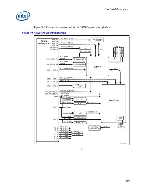
Figure 10-7 illustrates the various clocks in the 945G Express chipset platform. Figure 10-7. System Clocking Example CK410 56-Pin SSOP CPU_1 / CPU_1# CPU_0 / CPU_0# ITP_SRC7 / ITP_SRC7 # SRC_1 / SRC_1# SRC_2 / SRC_2# SRC_3 / SRC_3# SRC_5 / SRC_5# SRC_4 / SRC_4# SRC_6 / SRC_6# DOT_96 / DOT_96# USB_48 / USB_48# REF 0 PCIF_1 PCIF_2 PCI_5 PCI_4 PCI_3 PCI_2 PCI_1 PCI_0 Processor Diff Pair Processor Diff Pair Processor Diff Pair PCI Express DIff Pair PCI Express DIff Pair PCI Express DIff Pair PCI Express DIff Pair SATA Diff Pair DOT 96 MHz Diff Pair USB 48 MHz REF 14 MHz REF 14 MHz REF 33 MHz REF 14 MHz PCI 33 MHz 25 MHz Xtal PCI 33 MHz PCI 33 MHz PCI 33 MHz PCI 33 MHz PCI 33 MHz PCI 33 MHz PCI 33 MHz PCI 33 MHz PCI 33 MHz PCI Express GFX PCI Express Slot PCI Express LAN SIO LPC AC 97 LAN TPM LPC FWH LPC PCI Slot PCI Slot ITP x16 PCI Express* § Processor AC 97 Bit Clock LCI Bit Clock (G)MCH Intel ® High Definition Audio FSB Functional Description 24 MHz Slot 0 Slot 1 DMI Memory Intel ® ICH7 Slot 2 Slot 3 OSC 32.768 kHz Sys_Clocking 259
- Page 207 and 208: Figure 9-1. System Address Ranges 4
- Page 209 and 210: Compatible SMRAM Address Range (A_0
- Page 211 and 212: 9.2 Main Memory Address Range (1 MB
- Page 213 and 214: 9.3 PCI Memory Address Range (TOLUD
- Page 215 and 216: 9.3.6 PCI Express* Graphics Attach
- Page 217 and 218: 9.4.1 SMM Space Definition System A
- Page 219 and 220: 9.4.5 SMM Space Decode and Transact
- Page 221 and 222: 9.4.12 Legacy VGA and I/O Range Dec
- Page 223 and 224: 10 Functional Description This chap
- Page 225 and 226: Interleaved Mode Functional Descrip
- Page 227 and 228: 667 MHz (PC 5300) (82945G/82945GC/8
- Page 229 and 230: 10.2.2.2 System Memory Supported Co
- Page 231 and 232: Functional Description Table 10-5.
- Page 233 and 234: 10.3 PCI Express* (Intel ® 82945G/
- Page 235 and 236: Figure 10-2. SDVO Conceptual Block
- Page 237 and 238: Figure 10-3. Concurrent SDVO / PCI
- Page 239 and 240: 10.5 Integrated Graphics Device (In
- Page 241 and 242: 10.5.3 4X Faster Setup Engine Funct
- Page 243 and 244: 10.5.4 Texture Engine Functional De
- Page 245 and 246: 10.5.4.8 Pixel Shader Functional De
- Page 247 and 248: Functional Description to determine
- Page 249 and 250: 10.5.6 2D Engine Functional Descrip
- Page 251 and 252: 10.5.8.1 Cursor Plane Functional De
- Page 253 and 254: Functional Description device is in
- Page 255 and 256: 10.6.2 Digital Display Interface Fu
- Page 257: 10.6.2.1.5 Control Bus Functional D
- Page 261 and 262: 11 Electrical Characteristics Elect
- Page 263 and 264: 11.1.1 Power Characteristics Table
- Page 265 and 266: Signal Group Electrical Characteris
- Page 267 and 268: 11.3 DC Characteristics Table 11-5.
- Page 269 and 270: Symbol Signal Group Electrical Char
- Page 271 and 272: Ballout and Package Information 12
- Page 273 and 274: Ballout and Package Information Fig
- Page 275 and 276: 12.2 Ballout Table Ballout and Pack
- Page 277 and 278: Ballout and Package Information EXP
- Page 279 and 280: Ballout and Package Information HA2
- Page 281 and 282: Ballout and Package Information HD6
- Page 283 and 284: Ballout and Package Information RSV
- Page 285 and 286: Ballout and Package Information SDM
- Page 287 and 288: Ballout and Package Information SDQ
- Page 289 and 290: Ballout and Package Information SDQ
- Page 291 and 292: Ballout and Package Information VCC
- Page 293 and 294: Ballout and Package Information VCC
- Page 295 and 296: Ballout and Package Information VCC
- Page 297 and 298: Ballout and Package Information VSS
- Page 299 and 300: Ballout and Package Information VSS
- Page 301 and 302: Ballout and Package Information VSS
- Page 303 and 304: Ballout and Package Information VSS
- Page 305 and 306: 12.3 Package § Ballout and Package
- Page 307 and 308: Ballout and Package Information Int
Figure 10-7 illustrates the various clocks in the <strong>945G</strong> <strong>Express</strong> chipset platform.<br />
Figure 10-7. System Clocking Example<br />
CK410<br />
56-Pin SSOP<br />
CPU_1 /<br />
CPU_1#<br />
CPU_0 /<br />
CPU_0#<br />
ITP_SRC7 /<br />
ITP_SRC7 #<br />
SRC_1 / SRC_1#<br />
SRC_2 / SRC_2#<br />
SRC_3 / SRC_3#<br />
SRC_5 / SRC_5#<br />
SRC_4 / SRC_4#<br />
SRC_6 / SRC_6#<br />
DOT_96 / DOT_96#<br />
USB_48 / USB_48#<br />
REF 0<br />
PCIF_1<br />
PCIF_2<br />
PCI_5<br />
PCI_4<br />
PCI_3<br />
PCI_2<br />
PCI_1<br />
PCI_0<br />
Processor Diff Pair<br />
Processor Diff Pair<br />
Processor Diff Pair<br />
PCI <strong>Express</strong><br />
DIff Pair<br />
PCI <strong>Express</strong><br />
DIff Pair<br />
PCI <strong>Express</strong> DIff Pair<br />
PCI <strong>Express</strong> DIff Pair<br />
SATA Diff Pair<br />
DOT 96 MHz Diff Pair<br />
USB 48 MHz<br />
REF 14 MHz<br />
REF 14 MHz<br />
REF 33 MHz<br />
REF 14 MHz<br />
PCI 33 MHz<br />
25 MHz Xtal<br />
PCI 33 MHz<br />
PCI 33 MHz<br />
PCI 33 MHz<br />
PCI 33 MHz<br />
PCI 33 MHz<br />
PCI 33 MHz<br />
PCI 33 MHz<br />
PCI 33 MHz<br />
PCI 33 MHz<br />
PCI <strong>Express</strong> GFX<br />
PCI <strong>Express</strong> Slot<br />
PCI <strong>Express</strong><br />
LAN<br />
SIO LPC<br />
AC 97<br />
LAN<br />
TPM LPC<br />
FWH LPC<br />
PCI Slot<br />
PCI Slot<br />
ITP<br />
x16 PCI <strong>Express</strong>*<br />
§<br />
Processor<br />
AC 97 Bit Clock<br />
LCI Bit Clock<br />
(G)MCH<br />
Intel ® High<br />
Definition Audio<br />
FSB<br />
Functional Description<br />
24 MHz<br />
Slot 0<br />
Slot 1<br />
DMI<br />
Memory<br />
Intel ® ICH7<br />
Slot 2<br />
Slot 3<br />
OSC<br />
32.768 kHz<br />
Sys_Clocking<br />
259


