Intel® 945G/945GZ/945GC/ 945P/945PL Express Chipset Family ...
Intel® 945G/945GZ/945GC/ 945P/945PL Express Chipset Family ... Intel® 945G/945GZ/945GC/ 945P/945PL Express Chipset Family ...
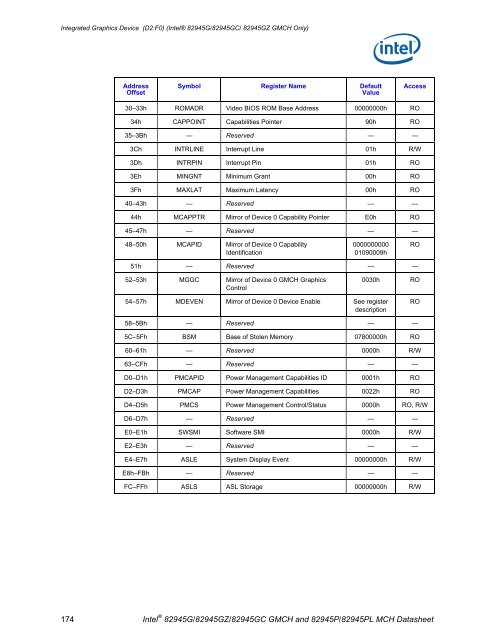
Integrated Graphics Device (D2:F0) (Intel® 82945G/82945GC/ 82945GZ GMCH Only) Address Offset Symbol Register Name Default Value Access 30–33h ROMADR Video BIOS ROM Base Address 00000000h RO 34h CAPPOINT Capabilities Pointer 90h RO 35–3Bh — Reserved — — 3Ch INTRLINE Interrupt Line 01h R/W 3Dh INTRPIN Interrupt Pin 01h RO 3Eh MINGNT Minimum Grant 00h RO 3Fh MAXLAT Maximum Latency 00h RO 40–43h — Reserved — — 44h MCAPPTR Mirror of Device 0 Capability Pointer E0h RO 45–47h — Reserved — — 48–50h MCAPID Mirror of Device 0 Capability Identification 0000000000 01090009h 51h — Reserved — — 52–53h MGGC Mirror of Device 0 GMCH Graphics Control 54–57h MDEVEN Mirror of Device 0 Device Enable See register description 174 Intel ® 82945G/82945GZ/82945GC GMCH and 82945P/82945PL MCH Datasheet RO 0030h RO 58–5Bh — Reserved — — 5C–5Fh BSM Base of Stolen Memory 07800000h RO 60–61h — Reserved 0000h R/W 63–CFh — Reserved — — D0–D1h PMCAPID Power Management Capabilities ID 0001h RO D2–D3h PMCAP Power Management Capabilities 0022h RO D4–D5h PMCS Power Management Control/Status 0000h RO, R/W D6–D7h — Reserved — — E0–E1h SWSMI Software SMI 0000h R/W E2–E3h — Reserved — — E4–E7h ASLE System Display Event 00000000h R/W E8h–FBh — Reserved — — FC–FFh ASLS ASL Storage 00000000h R/W RO
Integrated Graphics Device (D2:F0) (Intel® 82945G/82945GC/ 82945GZ GMCH Only) 7.1 Configuration Register Details (D2:F0) 7.1.1 VID2—Vendor Identification (D2:F0) PCI Device: 2 Address Offset: 00h Default Value: 8086h Access: RO Size: 16 bits This register, combined with the Device Identification register, uniquely identifies any PCI device. Bit Access & Default 15:0 RO 8086h Description Vendor Identification Number (VID): This field provides the PCI standard identification for Intel. 7.1.2 DID2—Device Identification (D2:F0) PCI Device: 2 Address Offset: 02h Default Value: 2772h Access: RO Size: 16 bits This register, combined with the Vendor Identification register, uniquely identifies any PCI device. Bit Access & Default 15:0 RO 2772h Description Device Identification Number (DID): This is a 16 bit value assigned to the GMCH Graphic device Intel ® 82945G/82945G/82945GC GMCH and 82945P/82945PL MCH Datasheet 175
- Page 123 and 124: Host-PCI Express* Bridge Registers
- Page 125 and 126: 5.1.20 INTRLINE1—Interrupt Line (
- Page 127 and 128: Bit Access & Default 2 R/W 0b 1 R/W
- Page 129 and 130: Host-PCI Express* Bridge Registers
- Page 131 and 132: Host-PCI Express* Bridge Registers
- Page 133 and 134: 5.1.29 MA—Message Address (D1:F0)
- Page 135 and 136: 5.1.33 DCAP—Device Capabilities (
- Page 137 and 138: 5.1.35 DSTS—Device Status (D1:F0)
- Page 139 and 140: 5.1.37 LCTL—Link Control (D1:F0)
- Page 141 and 142: 5.1.39 SLOTCAP—Slot Capabilities
- Page 143 and 144: 5.1.41 SLOTSTS—Slot Status (D1:F0
- Page 145 and 146: 5.1.43 RSTS—Root Status (D1:F0) P
- Page 147 and 148: Host-PCI Express* Bridge Registers
- Page 149 and 150: Host-PCI Express* Bridge Registers
- Page 151 and 152: Host-PCI Express* Bridge Registers
- Page 153 and 154: 5.1.56 ESD—Element Self Descripti
- Page 155 and 156: Host-PCI Express* Bridge Registers
- Page 157 and 158: 5.1.61 CESTS—Correctable Error St
- Page 159 and 160: Host-PCI Express* Bridge Registers
- Page 161 and 162: Direct Media Interface (DMI) RCRB 6
- Page 163 and 164: 6.1.3 DMIPVCCAP2—DMI Port VC Capa
- Page 165 and 166: 6.1.6 DMIVC0RCTL—DMI VC0 Resource
- Page 167 and 168: 6.1.9 DMIVC1RCTL—DMI VC1 Resource
- Page 169 and 170: 6.1.13 DMILSTS—DMI Link Status MM
- Page 171 and 172: 6.1.15 DMIUEMSK—DMI Uncorrectable
- Page 173: Integrated Graphics Device (D2:F0)
- Page 177 and 178: 7.1.4 PCISTS2—PCI Status (D2:F0)
- Page 179 and 180: 7.1.7 CLS—Cache Line Size (D2:F0)
- Page 181 and 182: 7.1.11 IOBAR—I/O Base Address (D2
- Page 183 and 184: Integrated Graphics Device (D2:F0)
- Page 185 and 186: 7.1.20 MINGNT—Minimum Grant (D2:F
- Page 187 and 188: Integrated Graphics Device (D2:F0)
- Page 189 and 190: Integrated Graphics Device (D2:F0)
- Page 191 and 192: Integrated Graphics Device (D2:F1)
- Page 193 and 194: 8.1.3 PCICMD2—PCI Command (D2:F1)
- Page 195 and 196: 8.1.5 RID2—Revision Identificatio
- Page 197 and 198: Integrated Graphics Device (D2:F1)
- Page 199 and 200: Integrated Graphics Device (D2:F1)
- Page 201 and 202: Integrated Graphics Device (D2:F1)
- Page 203 and 204: 8.2 Device 2 - PCI I/O Registers In
- Page 205 and 206: 9 System Address Map System Address
- Page 207 and 208: Figure 9-1. System Address Ranges 4
- Page 209 and 210: Compatible SMRAM Address Range (A_0
- Page 211 and 212: 9.2 Main Memory Address Range (1 MB
- Page 213 and 214: 9.3 PCI Memory Address Range (TOLUD
- Page 215 and 216: 9.3.6 PCI Express* Graphics Attach
- Page 217 and 218: 9.4.1 SMM Space Definition System A
- Page 219 and 220: 9.4.5 SMM Space Decode and Transact
- Page 221 and 222: 9.4.12 Legacy VGA and I/O Range Dec
- Page 223 and 224: 10 Functional Description This chap
Integrated Graphics Device (D2:F0) (<strong>Intel®</strong> 82<strong>945G</strong>/82<strong>945G</strong>C/ 82<strong>945G</strong>Z GMCH Only)<br />
Address<br />
Offset<br />
Symbol Register Name Default<br />
Value<br />
Access<br />
30–33h ROMADR Video BIOS ROM Base Address 00000000h RO<br />
34h CAPPOINT Capabilities Pointer 90h RO<br />
35–3Bh — Reserved — —<br />
3Ch INTRLINE Interrupt Line 01h R/W<br />
3Dh INTRPIN Interrupt Pin 01h RO<br />
3Eh MINGNT Minimum Grant 00h RO<br />
3Fh MAXLAT Maximum Latency 00h RO<br />
40–43h — Reserved — —<br />
44h MCAPPTR Mirror of Device 0 Capability Pointer E0h RO<br />
45–47h — Reserved — —<br />
48–50h MCAPID Mirror of Device 0 Capability<br />
Identification<br />
0000000000<br />
01090009h<br />
51h — Reserved — —<br />
52–53h MGGC Mirror of Device 0 GMCH Graphics<br />
Control<br />
54–57h MDEVEN Mirror of Device 0 Device Enable See register<br />
description<br />
174 Intel ® 82<strong>945G</strong>/82<strong>945G</strong>Z/82<strong>945G</strong>C GMCH and 82<strong>945P</strong>/82<strong>945P</strong>L MCH Datasheet<br />
RO<br />
0030h RO<br />
58–5Bh — Reserved — —<br />
5C–5Fh BSM Base of Stolen Memory 07800000h RO<br />
60–61h — Reserved 0000h R/W<br />
63–CFh — Reserved — —<br />
D0–D1h PMCAPID Power Management Capabilities ID 0001h RO<br />
D2–D3h PMCAP Power Management Capabilities 0022h RO<br />
D4–D5h PMCS Power Management Control/Status 0000h RO, R/W<br />
D6–D7h — Reserved — —<br />
E0–E1h SWSMI Software SMI 0000h R/W<br />
E2–E3h — Reserved — —<br />
E4–E7h ASLE System Display Event 00000000h R/W<br />
E8h–FBh — Reserved — —<br />
FC–FFh ASLS ASL Storage 00000000h R/W<br />
RO


