Intel® 945G/945GZ/945GC/ 945P/945PL Express Chipset Family ...
Intel® 945G/945GZ/945GC/ 945P/945PL Express Chipset Family ... Intel® 945G/945GZ/945GC/ 945P/945PL Express Chipset Family ...
Host-PCI Express* Bridge Registers (D1:F0) (Intel® 82945G/82945GC/82945P/82945PL Only) 160 Intel ® 82945G/82945GZ/82945GC GMCH and 82945P/82945PL MCH Datasheet
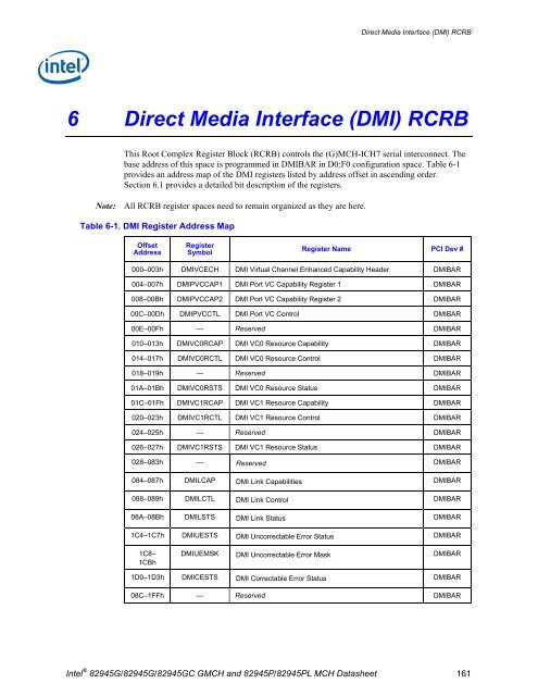
Direct Media Interface (DMI) RCRB 6 Direct Media Interface (DMI) RCRB This Root Complex Register Block (RCRB) controls the (G)MCH-ICH7 serial interconnect. The base address of this space is programmed in DMIBAR in D0:F0 configuration space. Table 6-1 provides an address map of the DMI registers listed by address offset in ascending order. Section 6.1 provides a detailed bit description of the registers. Note: All RCRB register spaces need to remain organized as they are here. Table 6-1. DMI Register Address Map Offset Address Register Symbol Register Name PCI Dev # 000–003h DMIVCECH DMI Virtual Channel Enhanced Capability Header DMIBAR 004–007h DMIPVCCAP1 DMI Port VC Capability Register 1 DMIBAR 008–00Bh DMIPVCCAP2 DMI Port VC Capability Register 2 DMIBAR 00C–00Dh DMIPVCCTL DMI Port VC Control DMIBAR 00E–00Fh — Reserved DMIBAR 010–013h DMIVC0RCAP DMI VC0 Resource Capability DMIBAR 014–017h DMIVC0RCTL DMI VC0 Resource Control DMIBAR 018–019h — Reserved DMIBAR 01A–01Bh DMIVC0RSTS DMI VC0 Resource Status DMIBAR 01C–01Fh DMIVC1RCAP DMI VC1 Resource Capability DMIBAR 020–023h DMIVC1RCTL DMI VC1 Resource Control DMIBAR 024–025h — Reserved DMIBAR 026–027h DMIVC1RSTS DMI VC1 Resource Status DMIBAR 028–083h — Reserved DMIBAR 084–087h DMILCAP DMI Link Capabilities DMIBAR 088–089h DMILCTL DMI Link Control DMIBAR 08A–08Bh DMILSTS DMI Link Status DMIBAR 1C4–1C7h DMIUESTS DMI Uncorrectable Error Status DMIBAR 1C8– 1CBh DMIUEMSK DMI Uncorrectable Error Mask DMIBAR 1D0–1D3h DMICESTS DMI Correctable Error Status DMIBAR 08C–1FFh — Reserved DMIBAR Intel ® 82945G/82945G/82945GC GMCH and 82945P/82945PL MCH Datasheet 161
- Page 109 and 110: Host-PCI Express* Bridge Registers
- Page 111 and 112: Address Offset Host-PCI Express* Br
- Page 113 and 114: 5.1.3 PCICMD1—PCI Command (D1:F0)
- Page 115 and 116: 5.1.4 PCISTS1—PCI Status (D1:F0)
- Page 117 and 118: 5.1.7 CL1—Cache Line Size (D1:F0)
- Page 119 and 120: 5.1.12 IOBASE1—I/O Base Address (
- Page 121 and 122: 5.1.15 MBASE1—Memory Base Address
- Page 123 and 124: Host-PCI Express* Bridge Registers
- Page 125 and 126: 5.1.20 INTRLINE1—Interrupt Line (
- Page 127 and 128: Bit Access & Default 2 R/W 0b 1 R/W
- Page 129 and 130: Host-PCI Express* Bridge Registers
- Page 131 and 132: Host-PCI Express* Bridge Registers
- Page 133 and 134: 5.1.29 MA—Message Address (D1:F0)
- Page 135 and 136: 5.1.33 DCAP—Device Capabilities (
- Page 137 and 138: 5.1.35 DSTS—Device Status (D1:F0)
- Page 139 and 140: 5.1.37 LCTL—Link Control (D1:F0)
- Page 141 and 142: 5.1.39 SLOTCAP—Slot Capabilities
- Page 143 and 144: 5.1.41 SLOTSTS—Slot Status (D1:F0
- Page 145 and 146: 5.1.43 RSTS—Root Status (D1:F0) P
- Page 147 and 148: Host-PCI Express* Bridge Registers
- Page 149 and 150: Host-PCI Express* Bridge Registers
- Page 151 and 152: Host-PCI Express* Bridge Registers
- Page 153 and 154: 5.1.56 ESD—Element Self Descripti
- Page 155 and 156: Host-PCI Express* Bridge Registers
- Page 157 and 158: 5.1.61 CESTS—Correctable Error St
- Page 159: Host-PCI Express* Bridge Registers
- Page 163 and 164: 6.1.3 DMIPVCCAP2—DMI Port VC Capa
- Page 165 and 166: 6.1.6 DMIVC0RCTL—DMI VC0 Resource
- Page 167 and 168: 6.1.9 DMIVC1RCTL—DMI VC1 Resource
- Page 169 and 170: 6.1.13 DMILSTS—DMI Link Status MM
- Page 171 and 172: 6.1.15 DMIUEMSK—DMI Uncorrectable
- Page 173 and 174: Integrated Graphics Device (D2:F0)
- Page 175 and 176: Integrated Graphics Device (D2:F0)
- Page 177 and 178: 7.1.4 PCISTS2—PCI Status (D2:F0)
- Page 179 and 180: 7.1.7 CLS—Cache Line Size (D2:F0)
- Page 181 and 182: 7.1.11 IOBAR—I/O Base Address (D2
- Page 183 and 184: Integrated Graphics Device (D2:F0)
- Page 185 and 186: 7.1.20 MINGNT—Minimum Grant (D2:F
- Page 187 and 188: Integrated Graphics Device (D2:F0)
- Page 189 and 190: Integrated Graphics Device (D2:F0)
- Page 191 and 192: Integrated Graphics Device (D2:F1)
- Page 193 and 194: 8.1.3 PCICMD2—PCI Command (D2:F1)
- Page 195 and 196: 8.1.5 RID2—Revision Identificatio
- Page 197 and 198: Integrated Graphics Device (D2:F1)
- Page 199 and 200: Integrated Graphics Device (D2:F1)
- Page 201 and 202: Integrated Graphics Device (D2:F1)
- Page 203 and 204: 8.2 Device 2 - PCI I/O Registers In
- Page 205 and 206: 9 System Address Map System Address
- Page 207 and 208: Figure 9-1. System Address Ranges 4
- Page 209 and 210: Compatible SMRAM Address Range (A_0
Direct Media Interface (DMI) RCRB<br />
6 Direct Media Interface (DMI) RCRB<br />
This Root Complex Register Block (RCRB) controls the (G)MCH-ICH7 serial interconnect. The<br />
base address of this space is programmed in DMIBAR in D0:F0 configuration space. Table 6-1<br />
provides an address map of the DMI registers listed by address offset in ascending order.<br />
Section 6.1 provides a detailed bit description of the registers.<br />
Note: All RCRB register spaces need to remain organized as they are here.<br />
Table 6-1. DMI Register Address Map<br />
Offset<br />
Address<br />
Register<br />
Symbol<br />
Register Name PCI Dev #<br />
000–003h DMIVCECH DMI Virtual Channel Enhanced Capability Header DMIBAR<br />
004–007h DMIPVCCAP1 DMI Port VC Capability Register 1 DMIBAR<br />
008–00Bh DMIPVCCAP2 DMI Port VC Capability Register 2 DMIBAR<br />
00C–00Dh DMIPVCCTL DMI Port VC Control DMIBAR<br />
00E–00Fh — Reserved DMIBAR<br />
010–013h DMIVC0RCAP DMI VC0 Resource Capability DMIBAR<br />
014–017h DMIVC0RCTL DMI VC0 Resource Control DMIBAR<br />
018–019h — Reserved DMIBAR<br />
01A–01Bh DMIVC0RSTS DMI VC0 Resource Status DMIBAR<br />
01C–01Fh DMIVC1RCAP DMI VC1 Resource Capability DMIBAR<br />
020–023h DMIVC1RCTL DMI VC1 Resource Control DMIBAR<br />
024–025h — Reserved DMIBAR<br />
026–027h DMIVC1RSTS DMI VC1 Resource Status DMIBAR<br />
028–083h — Reserved DMIBAR<br />
084–087h DMILCAP DMI Link Capabilities DMIBAR<br />
088–089h DMILCTL DMI Link Control DMIBAR<br />
08A–08Bh DMILSTS DMI Link Status DMIBAR<br />
1C4–1C7h DMIUESTS DMI Uncorrectable Error Status DMIBAR<br />
1C8–<br />
1CBh<br />
DMIUEMSK DMI Uncorrectable Error Mask DMIBAR<br />
1D0–1D3h DMICESTS DMI Correctable Error Status DMIBAR<br />
08C–1FFh — Reserved DMIBAR<br />
Intel ® 82<strong>945G</strong>/82<strong>945G</strong>/82<strong>945G</strong>C GMCH and 82<strong>945P</strong>/82<strong>945P</strong>L MCH Datasheet 161


