Intel® 945G/945GZ/945GC/ 945P/945PL Express Chipset Family ...
Intel® 945G/945GZ/945GC/ 945P/945PL Express Chipset Family ... Intel® 945G/945GZ/945GC/ 945P/945PL Express Chipset Family ...
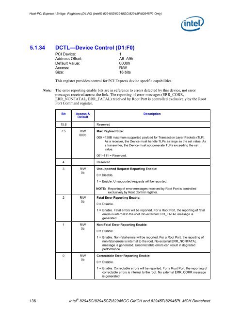
Host-PCI Express* Bridge Registers (D1:F0) (Intel® 82945G/82945GC/82945P/82945PL Only) 5.1.34 DCTL—Device Control (D1:F0) PCI Device: 1 Address Offset: A8–A9h Default Value: 0000h Access: R/W Size: 16 bits This register provides control for PCI Express device specific capabilities. Note: The error reporting enable bits are in reference to errors detected by this device, not error messages received across the link. The reporting of error messages (ERR_CORR, ERR_NONFATAL, ERR_FATAL) received by Root Port is controlled exclusively by the Root Port Command register. Bit Access & Default 15:8 Reserved 7:5 R/W 000b 4 Reserved 3 R/W 0b 2 R/W 0b 1 R/W 0b 0 R/W 0b Max Payload Size: Description 000 = 128B maximum supported payload for Transaction Layer Packets (TLP). As a receiver, the Device must handle TLPs as large as the set value. As a transmitter, the Device must not generate TLPs exceeding the set value. 001–111 = Reserved. Unsupported Request Reporting Enable: 0 = Disable. 1 = Enable. Unsupported requests will be reported. NOTE: Reporting of error messages received by Root Port is controlled exclusively by Root Control register. Fatal Error Reporting Enable: 0 = Disable. 1 = Enable. Fatal errors will be reported. For a Root Port, the reporting of fatal errors is internal to the root. No external ERR_FATAL message is generated. Non-Fatal Error Reporting Enable: 0 = Disable. 1 = Enable. Non-fatal errors will be reported. For a Root Port, the reporting of non-fatal errors is internal to the root. No external ERR_NONFATAL message is generated. Uncorrectable errors can result in degraded performance. Correctable Error Reporting Enable: 0 = Disable. 1 = Enable. Correctable errors will be reported. For a Root Port, the reporting of correctable errors is internal to the root. No external ERR_CORR message is generated. 136 Intel ® 82945G/82945GZ/82945GC GMCH and 82945P/82945PL MCH Datasheet
5.1.35 DSTS—Device Status (D1:F0) PCI Device: 1 Address Offset: AAh Default Value: 0000h Access: RO Size: 16 bits Host-PCI Express* Bridge Registers (D1:F0) (Intel® 82945G/82945GC/82945P/82945PL Only) This register reflects the status corresponding to controls in the Device Control register. Note: The error reporting bits are in reference to errors detected by this device, not errors messages received across the link. Bit Access & Default 15:6 Reserved 5 RO 0b 4 Reserved 3 R/WC 0b 2 R/WC 0b 1 R/WC 0b 0 R/WC 0b Transactions Pending: Description 0 = All pending transactions (including completions for any outstanding nonposted requests on any used virtual channel) have been completed. 1 = Device has transaction(s) pending (including completions for any outstanding non-posted requests for all used traffic classes). Unsupported Request Detected: 0 = Unsupported Request Not detected. 1 = Device received an Unsupported Request. Errors are logged in this register regardless of whether error reporting is enabled or not in the Device Control register. Fatal Error Detected: When Advanced Error Handling is enabled, errors are logged in this register regardless of the settings of the Correctable Error Mask register. 0 = Fatal Error Not detected. 1 = Fatal error(s) detected. Errors are logged in this register regardless of whether error reporting is enabled or not in the Device Control register. Non-Fatal Error Detected: When Advanced Error Handling is enabled, errors are logged in this register regardless of the settings of the Correctable Error Mask register. 0 = Non-fatal error Not detected. 1 = Non-fatal error(s) detected. Errors are logged in this register regardless of whether error reporting is enabled or not in the Device Control register. Correctable Error Detected: When Advanced Error Handling is enabled, errors are logged in this register regardless of the settings of the Correctable Error Mask register. 0 = Correctable error Not detected. 1 = Correctable error(s) detected. Errors are logged in this register regardless of whether error reporting is enabled or not in the Device Control register. Intel ® 82945G/82945G/82945GC GMCH and 82945P/82945PL MCH Datasheet 137
- Page 85 and 86: Host Bridge/DRAM Controller Registe
- Page 87 and 88: 4.1.29 ERRSTS—Error Status (D0:F0
- Page 89 and 90: 4.1.31 SKPD—Scratchpad Data (D0:F
- Page 91 and 92: Host Bridge/DRAM Controller Registe
- Page 93 and 94: Host Bridge/DRAM Controller Registe
- Page 95 and 96: 4.2.7 C0DCLKDIS—Channel A DRAM Cl
- Page 97 and 98: 4.2.9 C0DRT1—Channel A DRAM Timin
- Page 99 and 100: Bit Access & Default 6:4 R/W 000b 3
- Page 101 and 102: Host Bridge/DRAM Controller Registe
- Page 103 and 104: 4.2.24 PMSTS—Power Management Sta
- Page 105 and 106: 4.3.1 EPESD—EP Element Self Descr
- Page 107 and 108: 4.3.3 EPLE1A—EP Link Entry 1 Addr
- Page 109 and 110: Host-PCI Express* Bridge Registers
- Page 111 and 112: Address Offset Host-PCI Express* Br
- Page 113 and 114: 5.1.3 PCICMD1—PCI Command (D1:F0)
- Page 115 and 116: 5.1.4 PCISTS1—PCI Status (D1:F0)
- Page 117 and 118: 5.1.7 CL1—Cache Line Size (D1:F0)
- Page 119 and 120: 5.1.12 IOBASE1—I/O Base Address (
- Page 121 and 122: 5.1.15 MBASE1—Memory Base Address
- Page 123 and 124: Host-PCI Express* Bridge Registers
- Page 125 and 126: 5.1.20 INTRLINE1—Interrupt Line (
- Page 127 and 128: Bit Access & Default 2 R/W 0b 1 R/W
- Page 129 and 130: Host-PCI Express* Bridge Registers
- Page 131 and 132: Host-PCI Express* Bridge Registers
- Page 133 and 134: 5.1.29 MA—Message Address (D1:F0)
- Page 135: 5.1.33 DCAP—Device Capabilities (
- Page 139 and 140: 5.1.37 LCTL—Link Control (D1:F0)
- Page 141 and 142: 5.1.39 SLOTCAP—Slot Capabilities
- Page 143 and 144: 5.1.41 SLOTSTS—Slot Status (D1:F0
- Page 145 and 146: 5.1.43 RSTS—Root Status (D1:F0) P
- Page 147 and 148: Host-PCI Express* Bridge Registers
- Page 149 and 150: Host-PCI Express* Bridge Registers
- Page 151 and 152: Host-PCI Express* Bridge Registers
- Page 153 and 154: 5.1.56 ESD—Element Self Descripti
- Page 155 and 156: Host-PCI Express* Bridge Registers
- Page 157 and 158: 5.1.61 CESTS—Correctable Error St
- Page 159 and 160: Host-PCI Express* Bridge Registers
- Page 161 and 162: Direct Media Interface (DMI) RCRB 6
- Page 163 and 164: 6.1.3 DMIPVCCAP2—DMI Port VC Capa
- Page 165 and 166: 6.1.6 DMIVC0RCTL—DMI VC0 Resource
- Page 167 and 168: 6.1.9 DMIVC1RCTL—DMI VC1 Resource
- Page 169 and 170: 6.1.13 DMILSTS—DMI Link Status MM
- Page 171 and 172: 6.1.15 DMIUEMSK—DMI Uncorrectable
- Page 173 and 174: Integrated Graphics Device (D2:F0)
- Page 175 and 176: Integrated Graphics Device (D2:F0)
- Page 177 and 178: 7.1.4 PCISTS2—PCI Status (D2:F0)
- Page 179 and 180: 7.1.7 CLS—Cache Line Size (D2:F0)
- Page 181 and 182: 7.1.11 IOBAR—I/O Base Address (D2
- Page 183 and 184: Integrated Graphics Device (D2:F0)
- Page 185 and 186: 7.1.20 MINGNT—Minimum Grant (D2:F
Host-PCI <strong>Express</strong>* Bridge Registers (D1:F0) (<strong>Intel®</strong> 82<strong>945G</strong>/82<strong>945G</strong>C/82<strong>945P</strong>/82<strong>945P</strong>L Only)<br />
5.1.34 DCTL—Device Control (D1:F0)<br />
PCI Device: 1<br />
Address Offset: A8–A9h<br />
Default Value: 0000h<br />
Access: R/W<br />
Size: 16 bits<br />
This register provides control for PCI <strong>Express</strong> device specific capabilities.<br />
Note: The error reporting enable bits are in reference to errors detected by this device, not error<br />
messages received across the link. The reporting of error messages (ERR_CORR,<br />
ERR_NONFATAL, ERR_FATAL) received by Root Port is controlled exclusively by the Root<br />
Port Command register.<br />
Bit Access &<br />
Default<br />
15:8 Reserved<br />
7:5 R/W<br />
000b<br />
4 Reserved<br />
3 R/W<br />
0b<br />
2 R/W<br />
0b<br />
1 R/W<br />
0b<br />
0 R/W<br />
0b<br />
Max Payload Size:<br />
Description<br />
000 = 128B maximum supported payload for Transaction Layer Packets (TLP).<br />
As a receiver, the Device must handle TLPs as large as the set value. As<br />
a transmitter, the Device must not generate TLPs exceeding the set<br />
value.<br />
001–111 = Reserved.<br />
Unsupported Request Reporting Enable:<br />
0 = Disable.<br />
1 = Enable. Unsupported requests will be reported.<br />
NOTE: Reporting of error messages received by Root Port is controlled<br />
exclusively by Root Control register.<br />
Fatal Error Reporting Enable:<br />
0 = Disable.<br />
1 = Enable. Fatal errors will be reported. For a Root Port, the reporting of fatal<br />
errors is internal to the root. No external ERR_FATAL message is<br />
generated.<br />
Non-Fatal Error Reporting Enable:<br />
0 = Disable.<br />
1 = Enable. Non-fatal errors will be reported. For a Root Port, the reporting of<br />
non-fatal errors is internal to the root. No external ERR_NONFATAL<br />
message is generated. Uncorrectable errors can result in degraded<br />
performance.<br />
Correctable Error Reporting Enable:<br />
0 = Disable.<br />
1 = Enable. Correctable errors will be reported. For a Root Port, the reporting of<br />
correctable errors is internal to the root. No external ERR_CORR message<br />
is generated.<br />
136 Intel ® 82<strong>945G</strong>/82<strong>945G</strong>Z/82<strong>945G</strong>C GMCH and 82<strong>945P</strong>/82<strong>945P</strong>L MCH Datasheet


