Intel® 945G/945GZ/945GC/ 945P/945PL Express Chipset Family ...
Intel® 945G/945GZ/945GC/ 945P/945PL Express Chipset Family ... Intel® 945G/945GZ/945GC/ 945P/945PL Express Chipset Family ...
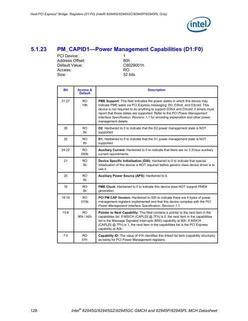
Host-PCI Express* Bridge Registers (D1:F0) (Intel® 82945G/82945GC/82945P/82945PL Only) 5.1.23 PM_CAPID1—Power Management Capabilities (D1:F0) PCI Device: 1 Address Offset: 80h Default Value: C8029001h Access: RO Size: 32 bits Bit Access & Default 31:27 RO 19h 26 RO 0b 25 RO 0b 24:22 RO 000b 21 RO 0b 20 RO 0b 19 RO 0b 18:16 RO 010b 15:8 RO 90h / A0h 7:0 RO 01h Description PME Support: This field indicates the power states in which this device may indicate PME wake via PCI Express messaging: D0, D3hot, and D3cold. This device is not required to do anything to support D3hot and D3cold; it simply must report that those states are supported. Refer to the PCI Power Management Interface Specification, Revision 1.1 for encoding explanation and other power management details. D2: Hardwired to 0 to indicate that the D2 power management state is NOT supported. D1: Hardwired to 0 to indicate that the D1 power management state is NOT supported. Auxiliary Current: Hardwired to 0 to indicate that there are no 3.3Vaux auxiliary current requirements. Device Specific Initialization (DSI): Hardwired to 0 to indicate that special initialization of this device is NOT required before generic class device driver is to use it. Auxiliary Power Source (APS): Hardwired to 0. PME Clock: Hardwired to 0 to indicate this device does NOT support PME# generation. PCI PM CAP Version: Hardwired to 02h to indicate there are 4 bytes of power management registers implemented and that this device complies with the PCI Power Management Interface Specification, Revision 1.1. Pointer to Next Capability: This filed contains a pointer to the next item in the capabilities list. If MSICH (CAPL[0] @ 7Fh) is 0, the next item in the capabilities list is the Message Signaled Interrupts (MSI) capability at 90h. If MSICH (CAPL[0] @ 7Fh) is 1, the next item in the capabilities list is the PCI Express capability at A0h. Capability ID: The value of 01h identifies this linked list item (capability structure) as being for PCI Power Management registers. 128 Intel ® 82945G/82945GZ/82945GC GMCH and 82945P/82945PL MCH Datasheet
Host-PCI Express* Bridge Registers (D1:F0) (Intel® 82945G/82945GC/82945P/82945PL Only) 5.1.24 PM_CS1—Power Management Control/Status (D1:F0) PCI Device: 1 Address Offset: 84–87h Default Value: 00000000h Access: RO, R/W/S Size: 32 bits Bit Access & Default 31:16 Reserved 15 RO 0b 14:13 RO 00b 12:9 RO 0h 8 R/W/S 0b 7:2 Reserved 1:0 R/W 00b Description PME Status: This bit indicates that this device does not support PME# generation from D3cold. Data Scale: This field indicates that this device does not support the Power Management Data register. Data Select: This field indicates that this device does not support the Power Management Data register. PME Enable: This bit indicates that this device does not generate PME# assertion from any D state. 0 = PMEB generation not possible from any D State 1 = PMEB generation enabled from any D State The setting of this bit has no effect on hardware. See PM_CAP[15:11] Power State: This field indicates the current power state of this device and can be used to set the device into a new power state. If software attempts to write an unsupported state to this field, write operation must complete normally on the bus, but the data is discarded and no state change occurs. 00 = D0 01 = D1 (Not supported in this device.) 10 = D2 (Not supported in this device.) 11 = D3. Support of D3cold does not require any special action. While in the D3hot state, this device can only act as the target of PCI configuration transactions (for power management control). This device also cannot generate interrupts or respond to MMR cycles in the D3 state. The device must return to the D0 state to be fully functional. There is no hardware functionality required to support these power states. Intel ® 82945G/82945G/82945GC GMCH and 82945P/82945PL MCH Datasheet 129
- Page 77 and 78: 4.1.19 PAM1—Programmable Attribut
- Page 79 and 80: 4.1.21 PAM3—Programmable Attribut
- Page 81 and 82: 4.1.23 PAM5—Programmable Attribut
- Page 83 and 84: 4.1.25 LAC—Legacy Access Control
- Page 85 and 86: Host Bridge/DRAM Controller Registe
- Page 87 and 88: 4.1.29 ERRSTS—Error Status (D0:F0
- Page 89 and 90: 4.1.31 SKPD—Scratchpad Data (D0:F
- Page 91 and 92: Host Bridge/DRAM Controller Registe
- Page 93 and 94: Host Bridge/DRAM Controller Registe
- Page 95 and 96: 4.2.7 C0DCLKDIS—Channel A DRAM Cl
- Page 97 and 98: 4.2.9 C0DRT1—Channel A DRAM Timin
- Page 99 and 100: Bit Access & Default 6:4 R/W 000b 3
- Page 101 and 102: Host Bridge/DRAM Controller Registe
- Page 103 and 104: 4.2.24 PMSTS—Power Management Sta
- Page 105 and 106: 4.3.1 EPESD—EP Element Self Descr
- Page 107 and 108: 4.3.3 EPLE1A—EP Link Entry 1 Addr
- Page 109 and 110: Host-PCI Express* Bridge Registers
- Page 111 and 112: Address Offset Host-PCI Express* Br
- Page 113 and 114: 5.1.3 PCICMD1—PCI Command (D1:F0)
- Page 115 and 116: 5.1.4 PCISTS1—PCI Status (D1:F0)
- Page 117 and 118: 5.1.7 CL1—Cache Line Size (D1:F0)
- Page 119 and 120: 5.1.12 IOBASE1—I/O Base Address (
- Page 121 and 122: 5.1.15 MBASE1—Memory Base Address
- Page 123 and 124: Host-PCI Express* Bridge Registers
- Page 125 and 126: 5.1.20 INTRLINE1—Interrupt Line (
- Page 127: Bit Access & Default 2 R/W 0b 1 R/W
- Page 131 and 132: Host-PCI Express* Bridge Registers
- Page 133 and 134: 5.1.29 MA—Message Address (D1:F0)
- Page 135 and 136: 5.1.33 DCAP—Device Capabilities (
- Page 137 and 138: 5.1.35 DSTS—Device Status (D1:F0)
- Page 139 and 140: 5.1.37 LCTL—Link Control (D1:F0)
- Page 141 and 142: 5.1.39 SLOTCAP—Slot Capabilities
- Page 143 and 144: 5.1.41 SLOTSTS—Slot Status (D1:F0
- Page 145 and 146: 5.1.43 RSTS—Root Status (D1:F0) P
- Page 147 and 148: Host-PCI Express* Bridge Registers
- Page 149 and 150: Host-PCI Express* Bridge Registers
- Page 151 and 152: Host-PCI Express* Bridge Registers
- Page 153 and 154: 5.1.56 ESD—Element Self Descripti
- Page 155 and 156: Host-PCI Express* Bridge Registers
- Page 157 and 158: 5.1.61 CESTS—Correctable Error St
- Page 159 and 160: Host-PCI Express* Bridge Registers
- Page 161 and 162: Direct Media Interface (DMI) RCRB 6
- Page 163 and 164: 6.1.3 DMIPVCCAP2—DMI Port VC Capa
- Page 165 and 166: 6.1.6 DMIVC0RCTL—DMI VC0 Resource
- Page 167 and 168: 6.1.9 DMIVC1RCTL—DMI VC1 Resource
- Page 169 and 170: 6.1.13 DMILSTS—DMI Link Status MM
- Page 171 and 172: 6.1.15 DMIUEMSK—DMI Uncorrectable
- Page 173 and 174: Integrated Graphics Device (D2:F0)
- Page 175 and 176: Integrated Graphics Device (D2:F0)
- Page 177 and 178: 7.1.4 PCISTS2—PCI Status (D2:F0)
Host-PCI <strong>Express</strong>* Bridge Registers (D1:F0) (<strong>Intel®</strong> 82<strong>945G</strong>/82<strong>945G</strong>C/82<strong>945P</strong>/82<strong>945P</strong>L Only)<br />
5.1.23 PM_CAPID1—Power Management Capabilities (D1:F0)<br />
PCI Device: 1<br />
Address Offset: 80h<br />
Default Value: C8029001h<br />
Access: RO<br />
Size: 32 bits<br />
Bit Access &<br />
Default<br />
31:27 RO<br />
19h<br />
26 RO<br />
0b<br />
25 RO<br />
0b<br />
24:22 RO<br />
000b<br />
21 RO<br />
0b<br />
20 RO<br />
0b<br />
19 RO<br />
0b<br />
18:16 RO<br />
010b<br />
15:8 RO<br />
90h / A0h<br />
7:0 RO<br />
01h<br />
Description<br />
PME Support: This field indicates the power states in which this device may<br />
indicate PME wake via PCI <strong>Express</strong> messaging: D0, D3hot, and D3cold. This<br />
device is not required to do anything to support D3hot and D3cold; it simply must<br />
report that those states are supported. Refer to the PCI Power Management<br />
Interface Specification, Revision 1.1 for encoding explanation and other power<br />
management details.<br />
D2: Hardwired to 0 to indicate that the D2 power management state is NOT<br />
supported.<br />
D1: Hardwired to 0 to indicate that the D1 power management state is NOT<br />
supported.<br />
Auxiliary Current: Hardwired to 0 to indicate that there are no 3.3Vaux auxiliary<br />
current requirements.<br />
Device Specific Initialization (DSI): Hardwired to 0 to indicate that special<br />
initialization of this device is NOT required before generic class device driver is to<br />
use it.<br />
Auxiliary Power Source (APS): Hardwired to 0.<br />
PME Clock: Hardwired to 0 to indicate this device does NOT support PME#<br />
generation.<br />
PCI PM CAP Version: Hardwired to 02h to indicate there are 4 bytes of power<br />
management registers implemented and that this device complies with the PCI<br />
Power Management Interface Specification, Revision 1.1.<br />
Pointer to Next Capability: This filed contains a pointer to the next item in the<br />
capabilities list. If MSICH (CAPL[0] @ 7Fh) is 0, the next item in the capabilities<br />
list is the Message Signaled Interrupts (MSI) capability at 90h. If MSICH<br />
(CAPL[0] @ 7Fh) is 1, the next item in the capabilities list is the PCI <strong>Express</strong><br />
capability at A0h.<br />
Capability ID: The value of 01h identifies this linked list item (capability structure)<br />
as being for PCI Power Management registers.<br />
128 Intel ® 82<strong>945G</strong>/82<strong>945G</strong>Z/82<strong>945G</strong>C GMCH and 82<strong>945P</strong>/82<strong>945P</strong>L MCH Datasheet


