Intel® 945G/945GZ/945GC/ 945P/945PL Express Chipset Family ...
Intel® 945G/945GZ/945GC/ 945P/945PL Express Chipset Family ... Intel® 945G/945GZ/945GC/ 945P/945PL Express Chipset Family ...
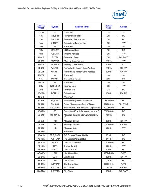
Host-PCI Express* Bridge Registers (D1:F0) (Intel® 82945G/82945GC/82945P/82945PL Only) Address Offset Symbol Register Name Default Value 0F–17h — Reserved — — Access 18h PBUSN1 Primary Bus Number 00h RO 19h SBUSN1 Secondary Bus Number 00h RO 1Ah SUBUSN1 Subordinate Bus Number 00h R/W 1Bh — Reserved — — 1Ch IOBASE1 I/O Base Address F0h RO 1Dh IOLIMIT1 I/O Limit Address 00h R/W 1Eh–1Fh SSTS1 Secondary Status 00h RO, R/WC 20–21h MBASE1 Memory Base Address FFF0h R/W 22–23h MLIMIT1 Memory Limit Address 0000h R/W 24–25h PMBASE1 Prefetchable Memory Base Address FFF0h RO, R/W 26–27h PMLIMIT1 Prefetchable Memory Limit Address 0000h RO, R/W 28–33h — Reserved — — 34h CAPPTR1 Capabilities Pointer 88h RO 35–3Bh — Reserved — — 3Ch INTRLINE1 Interrupt Line 00h R/W 3Dh INTRPIN1 Interrupt Pin 01h RO 3E–3Fh BCTRL1 Bridge Control 0000h RO, R/W 40–7Fh — Reserved — — 80–83h PM_CAP1 Power Management Capabilities C8029001h RO 84–87h PM_CS1 Power Management Control/Status 00000000h RO, R/W/S 88–8Bh SS_CAPID Subsystem ID and Vendor ID Capabilities 0000800Dh RO 8C–8Fh SS Subsystem ID and Subsystem Vendor ID 00008086h RO 90–91h MSI_CAPID Message Signaled Interrupts Capability ID A005h RO 92–93h MC Message Control 0000h RO, R/W 94–97h MA Message Address 00000000h RO, R/W 98–99h MD Message Data 0000h R/W 9A–9Fh — Reserved — — A0–A1h PEG_CAPL PCI Express* Capability List 0010h RO A2–A3h PEG_CAP PCI Express* Capabilities 0141h RO A4–A7h DCAP Device Capabilities 00000000h RO A8–A9h DCTL Device Control 0000h R/W AA–ABh DSTS Device Status 0000h RO AC–AFh LCAP Link Capabilities 02014D01h R/WO B0–B1h LCTL Link Control 0000h RO, R/W B2–B3h LSTS Link Status 1001h RO B4–B7h SLOTCAP Slot Capabilities 00000000h R/WO B8–B9h SLOTCTL Slot Control 01C0h RO, R/W BA–BBh SLOTSTS Slot Status 0000h RO, R/WC 110 Intel ® 82945G/82945GZ/82945GC GMCH and 82945P/82945PL MCH Datasheet
Address Offset Host-PCI Express* Bridge Registers (D1:F0) (Intel® 82945G/82945GC/82945P/82945PL Only) Symbol Register Name Default Value Access BC–BDh RCTL Root Control 0000h R/W BE–BFh — Reserved — — C0–C3h RSTS Root Status 00000000h RO, R/WC C4–FFh — Reserved — — EC–EFh PEG_LC PCI Express* Legacy Control 00000000h R/W 100–103h VCECH Virtual Channel Enhanced Capability Header 14010002h RO 104–107h PVCCAP1 Port VC Capability Register 1 00000001h RO, R/WO 108–10Bh PVCCAP2 Port VC Capability Register 2 00000001h RO 10C–10Dh PVCCTL Port VC Control 0000h R/W 10E–10Fh — Reserved — — 110–113h VC0RCAP VC0 Resource Capability 00000000h RO 114–117h VC0RCTL VC0 Resource Control 800000FFh RO, R/W 118–119h — Reserved — — 11A–11Bh VC0RSTS VC0 Resource Status 0002h RO 11C–11Fh VC1RCAP VC1 Resource Capability 00008000h RO 120–123h VC1RCTL VC1 Resource Control 01000000h RO, R/W 124–125h — Reserved — — 126–127h VC1RSTS VC1 Resource Status 0002h RO 128–13Fh — Reserved — — 140–143h RCLDECH Root Complex Link Declaration Enhanced Capability Header 00010005h RO 144–147h ESD Element Self Description 02000100h RO, R/WO 148–14Fh — Reserved — — 150–153h LE1D Link Entry 1 Description 00000000h RO, R/WO 154–157h — Reserved — — 158–15Fh LE1A Link Entry 1 Address 0000000000 000000h 160–1C5h — Reserved — — Intel ® 82945G/82945G/82945GC GMCH and 82945P/82945PL MCH Datasheet 111 R/WO 1C4–1C7h UESTS Uncorrectable Error Status 00000000h RO, R/WC/S 1C8–1CBh UEMSK Uncorrectable Error Mask 00000000h RO, R/W/S 1D0–1D3h CESTS Correctable Error Status 00000000h RO, R/W/S 1D4–1D3h — Reserved — — 1D4–1D7h CEMSK Correctable Error Mask 00000000h R/W/S 1D8–217h — Reserved — — 218–21Fh PEG_SSTS PCI Express* Sequence Status 0000000000 000FFFh 220–FFFh — Reserved — — RO
- Page 59 and 60: Bit Access & Default 10:8 R/W 000b
- Page 61 and 62: Host Bridge/DRAM Controller Registe
- Page 63 and 64: 4.1 Device 0 Configuration Register
- Page 65 and 66: 4.1.4 PCISTS—PCI Status (D0:F0) P
- Page 67 and 68: 4.1.7 MLT—Master Latency Timer (D
- Page 69 and 70: 4.1.12 EPBAR—Egress Port Base Add
- Page 71 and 72: Host Bridge/DRAM Controller Registe
- Page 73 and 74: Host Bridge/DRAM Controller Registe
- Page 75 and 76: Host Bridge/DRAM Controller Registe
- Page 77 and 78: 4.1.19 PAM1—Programmable Attribut
- Page 79 and 80: 4.1.21 PAM3—Programmable Attribut
- Page 81 and 82: 4.1.23 PAM5—Programmable Attribut
- Page 83 and 84: 4.1.25 LAC—Legacy Access Control
- Page 85 and 86: Host Bridge/DRAM Controller Registe
- Page 87 and 88: 4.1.29 ERRSTS—Error Status (D0:F0
- Page 89 and 90: 4.1.31 SKPD—Scratchpad Data (D0:F
- Page 91 and 92: Host Bridge/DRAM Controller Registe
- Page 93 and 94: Host Bridge/DRAM Controller Registe
- Page 95 and 96: 4.2.7 C0DCLKDIS—Channel A DRAM Cl
- Page 97 and 98: 4.2.9 C0DRT1—Channel A DRAM Timin
- Page 99 and 100: Bit Access & Default 6:4 R/W 000b 3
- Page 101 and 102: Host Bridge/DRAM Controller Registe
- Page 103 and 104: 4.2.24 PMSTS—Power Management Sta
- Page 105 and 106: 4.3.1 EPESD—EP Element Self Descr
- Page 107 and 108: 4.3.3 EPLE1A—EP Link Entry 1 Addr
- Page 109: Host-PCI Express* Bridge Registers
- Page 113 and 114: 5.1.3 PCICMD1—PCI Command (D1:F0)
- Page 115 and 116: 5.1.4 PCISTS1—PCI Status (D1:F0)
- Page 117 and 118: 5.1.7 CL1—Cache Line Size (D1:F0)
- Page 119 and 120: 5.1.12 IOBASE1—I/O Base Address (
- Page 121 and 122: 5.1.15 MBASE1—Memory Base Address
- Page 123 and 124: Host-PCI Express* Bridge Registers
- Page 125 and 126: 5.1.20 INTRLINE1—Interrupt Line (
- Page 127 and 128: Bit Access & Default 2 R/W 0b 1 R/W
- Page 129 and 130: Host-PCI Express* Bridge Registers
- Page 131 and 132: Host-PCI Express* Bridge Registers
- Page 133 and 134: 5.1.29 MA—Message Address (D1:F0)
- Page 135 and 136: 5.1.33 DCAP—Device Capabilities (
- Page 137 and 138: 5.1.35 DSTS—Device Status (D1:F0)
- Page 139 and 140: 5.1.37 LCTL—Link Control (D1:F0)
- Page 141 and 142: 5.1.39 SLOTCAP—Slot Capabilities
- Page 143 and 144: 5.1.41 SLOTSTS—Slot Status (D1:F0
- Page 145 and 146: 5.1.43 RSTS—Root Status (D1:F0) P
- Page 147 and 148: Host-PCI Express* Bridge Registers
- Page 149 and 150: Host-PCI Express* Bridge Registers
- Page 151 and 152: Host-PCI Express* Bridge Registers
- Page 153 and 154: 5.1.56 ESD—Element Self Descripti
- Page 155 and 156: Host-PCI Express* Bridge Registers
- Page 157 and 158: 5.1.61 CESTS—Correctable Error St
- Page 159 and 160: Host-PCI Express* Bridge Registers
Host-PCI <strong>Express</strong>* Bridge Registers (D1:F0) (<strong>Intel®</strong> 82<strong>945G</strong>/82<strong>945G</strong>C/82<strong>945P</strong>/82<strong>945P</strong>L Only)<br />
Address<br />
Offset<br />
Symbol Register Name<br />
Default<br />
Value<br />
0F–17h — Reserved — —<br />
Access<br />
18h PBUSN1 Primary Bus Number 00h RO<br />
19h SBUSN1 Secondary Bus Number 00h RO<br />
1Ah SUBUSN1 Subordinate Bus Number 00h R/W<br />
1Bh — Reserved — —<br />
1Ch IOBASE1 I/O Base Address F0h RO<br />
1Dh IOLIMIT1 I/O Limit Address 00h R/W<br />
1Eh–1Fh SSTS1 Secondary Status 00h RO, R/WC<br />
20–21h MBASE1 Memory Base Address FFF0h R/W<br />
22–23h MLIMIT1 Memory Limit Address 0000h R/W<br />
24–25h PMBASE1 Prefetchable Memory Base Address FFF0h RO, R/W<br />
26–27h PMLIMIT1 Prefetchable Memory Limit Address 0000h RO, R/W<br />
28–33h — Reserved — —<br />
34h CAPPTR1 Capabilities Pointer 88h RO<br />
35–3Bh — Reserved — —<br />
3Ch INTRLINE1 Interrupt Line 00h R/W<br />
3Dh INTRPIN1 Interrupt Pin 01h RO<br />
3E–3Fh BCTRL1 Bridge Control 0000h RO, R/W<br />
40–7Fh — Reserved — —<br />
80–83h PM_CAP1 Power Management Capabilities C8029001h RO<br />
84–87h PM_CS1 Power Management Control/Status 00000000h RO, R/W/S<br />
88–8Bh SS_CAPID Subsystem ID and Vendor ID Capabilities 0000800Dh RO<br />
8C–8Fh SS Subsystem ID and Subsystem Vendor ID 00008086h RO<br />
90–91h MSI_CAPID Message Signaled Interrupts Capability<br />
ID<br />
A005h RO<br />
92–93h MC Message Control 0000h RO, R/W<br />
94–97h MA Message Address 00000000h RO, R/W<br />
98–99h MD Message Data 0000h R/W<br />
9A–9Fh — Reserved — —<br />
A0–A1h PEG_CAPL PCI <strong>Express</strong>* Capability List 0010h RO<br />
A2–A3h PEG_CAP PCI <strong>Express</strong>* Capabilities 0141h RO<br />
A4–A7h DCAP Device Capabilities 00000000h RO<br />
A8–A9h DCTL Device Control 0000h R/W<br />
AA–ABh DSTS Device Status 0000h RO<br />
AC–AFh LCAP Link Capabilities 02014D01h R/WO<br />
B0–B1h LCTL Link Control 0000h RO, R/W<br />
B2–B3h LSTS Link Status 1001h RO<br />
B4–B7h SLOTCAP Slot Capabilities 00000000h R/WO<br />
B8–B9h SLOTCTL Slot Control 01C0h RO, R/W<br />
BA–BBh SLOTSTS Slot Status 0000h RO, R/WC<br />
110 Intel ® 82<strong>945G</strong>/82<strong>945G</strong>Z/82<strong>945G</strong>C GMCH and 82<strong>945P</strong>/82<strong>945P</strong>L MCH Datasheet


