DATA SHEET - Glyn High-Tech Distribution
DATA SHEET - Glyn High-Tech Distribution DATA SHEET - Glyn High-Tech Distribution
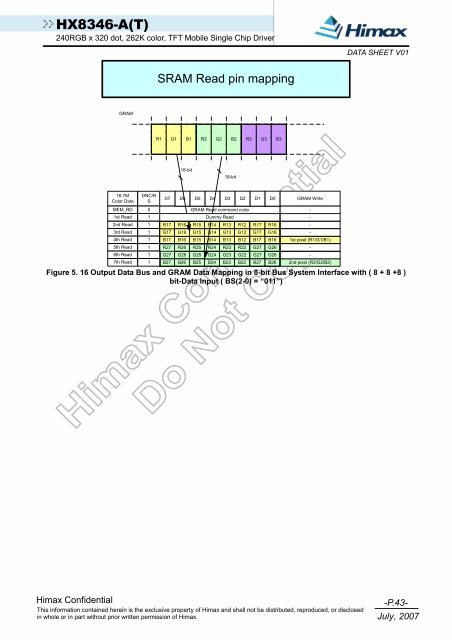
HX8346-A(T)240RGB x 320 dot, 262K color, TFT Mobile Single Chip DriverDATA SHEET V01SRAM Read pin mappingGRAMR1 G1 B1 R2 G2 B2 R3 G3 B318-bit18-bit16.7MColor DataMEM_RDDNC/RSD7D6 D5 D4 D3 D2 D1 D0GRAM Write0GRAM Read command code-1st Read 1 Dummy Read-2nd Read3rd Read11R17G17R16G16R15G15R14G14R13G13R12G12R17G17R16G16--4th Read 1 B17 B16 B15 B14 B13 B12 B17 B16 1st pixel (R1/G1/B1)5th Read 1 R27 R26 R25 R24 R23 R22 G27 G26-6th Read 1 G27 G26 G25 G24 G23 G22 G27 G26-7th Read 1 B27 B26 B25 B24 B23 B22 B27 B26 2nd pixel (R2/G2/B2)Figure 5. 16 Output Data Bus and GRAM Data Mapping in 8-bit Bus System Interface with ( 8 + 8 +8 )bit-Data Input ( BS(2-0) = “011”)Himax ConfidentialThis information contained herein is the exclusive property of Himax and shall not be distributed, reproduced, or disclosedin whole or in part without prior written permission of Himax.-P.43-July, 2007
HX8346-A(T)240RGB x 320 dot, 262K color, TFT Mobile Single Chip Driver5.1.1.2 Serial Bus System InterfaceDATA SHEET V01The HX8346-A supports the serial bus interface in register-content mode by settingexternal pins “BS2, BS1” pins to “11”. The serial bus system interface mode isenabled through the chip select line (NCS), and accessed via a control consisting ofthe serial input data (SDI), serial output data (SDO), and the serial transfer clocksignal (DNC_SCL).As the chip select signal (NCS) goes low, the start byte needs to be transferred first.The start byte is made up of 6-bit bus device identification code, register select (RS)bit and read /write operation (RW) bit. The five upper bits of 6-bit bus deviceidentification code must be set to “01110”, and the least significant bit of theidentification code must be set as the external pin BS0 input as “ID”.The seventh bit (RS) of the start byte determine internal index register or register,GRAM accessing. It must be setting RS as “0” when write data to the index register orread the status, and it must be setting RS as “1” when write a command or GRAMdata. The read or write operation is selected by the eighth bit (RW). The Table 5.6 isspecified the function of RS and R/W bit.RS R/W Function0 0 Writes Indexes into IR1 0 Writes command into register or data into GRAM1 1 Reads command from register or data from GRAMTable 5. 6 The Function of RS and R/W BitHimax ConfidentialThis information contained herein is the exclusive property of Himax and shall not be distributed, reproduced, or disclosedin whole or in part without prior written permission of Himax.-P.44-July, 2007
- Page 1 and 2: DATA SHEET( DOC No. HX8346-A(T)-DS
- Page 3 and 4: HX8346-A(T)240RGB x 320 dot, 262K c
- Page 5 and 6: HX8346-A(T)240RGB x 320 dot, 262K c
- Page 7 and 8: HX8346-A(T)240RGB x 320 dot, 262K c
- Page 9 and 10: HX8346-A(T)240RGB x 320 dot, 262K c
- Page 11 and 12: HX8346-A240RGB x 320 dot, 262K colo
- Page 13 and 14: HX8346-A(T)240RGB x 320 dot, 262K c
- Page 15 and 16: HX8346-A(T)240RGB x 320 dot, 262K c
- Page 17 and 18: HX8346-A(T)240RGB x 320 dot, 262K c
- Page 19 and 20: HX8346-A(T)240RGB x 320 dot, 262K c
- Page 21 and 22: NO.1NO.302PADA1PADB1DUMMYR1DUMMYR2P
- Page 23 and 24: HX8346-A(T)240RGB x 320 dot, 262K c
- Page 25 and 26: HX8346-A(T)240RGB x 320 dot, 262K c
- Page 27 and 28: HX8346-A(T)240RGB x 320 dot, 262K c
- Page 29 and 30: HX8346-A(T)240RGB x 320 dot, 262K c
- Page 31 and 32: HX8346-A(T)240RGB x 320 dot, 262K c
- Page 33 and 34: HX8346-A(T)240RGB x 320 dot, 262K c
- Page 35 and 36: HX8346-A(T)240RGB x 320 dot, 262K c
- Page 37 and 38: HX8346-A(T)240RGB x 320 dot, 262K c
- Page 39 and 40: HX8346-A(T)240RGB x 320 dot, 262K c
- Page 41 and 42: HX8346-A(T)240RGB x 320 dot, 262K c
- Page 43: HX8346-A(T)240RGB x 320 dot, 262K c
- Page 47 and 48: HX8346-A(T)240RGB x 320 dot, 262K c
- Page 49 and 50: HX8346-A(T)240RGB x 320 dot, 262K c
- Page 51 and 52: HX8346-A(T)240RGB x 320 dot, 262K c
- Page 53 and 54: HX8346-A(T)240RGB x 320 dot, 262K c
- Page 55 and 56: HX8346-A(T)240RGB x 320 dot, 262K c
- Page 57 and 58: HX8346-A(T)240RGB x 320 dot, 262K c
- Page 59 and 60: HX8346-A(T)240RGB x 320 dot, 262K c
- Page 61 and 62: HX8346-A(T)240RGB x 320 dot, 262K c
- Page 63 and 64: HX8346-A(T)240RGB x 320 dot, 262K c
- Page 65 and 66: HX8346-A(T)240RGB x 320 dot, 262K c
- Page 67 and 68: HX8346-A(T)240RGB x 320 dot, 262K c
- Page 69 and 70: HX8346-A(T)240RGB x 320 dot, 262K c
- Page 71 and 72: HX8346-A(T)240RGB x 320 dot, 262K c
- Page 73 and 74: HX8346-A(T)240RGB x 320 dot, 262K c
- Page 75 and 76: HX8346-A(T)240RGB x 320 dot, 262K c
- Page 77 and 78: HX8346-A(T)240RGB x 320 dot, 262K c
- Page 79 and 80: HX8346-A(T)240RGB x 320 dot, 262K c
- Page 81 and 82: HX8346-A(T)240RGB x 320 dot, 262K c
- Page 83 and 84: HX8346-A(T)240RGBx320 dots, 262,144
- Page 85 and 86: HX8346-A(T)240RGBx320 dots, 262K co
- Page 87 and 88: HX8346-A(T)240RGBx320 dots, 262K co
- Page 89 and 90: HX8346-A(T)240RGBx320 dots, 262K co
- Page 91 and 92: HX8346-A(T)240RGBx320 dots, 262K co
- Page 93 and 94: HX8346-A(T)240RGBx320 dots, 262K co
HX8346-A(T)240RGB x 320 dot, 262K color, TFT Mobile Single Chip Driver<strong>DATA</strong> <strong>SHEET</strong> V01SRAM Read pin mappingGRAMR1 G1 B1 R2 G2 B2 R3 G3 B318-bit18-bit16.7MColor DataMEM_RDDNC/RSD7D6 D5 D4 D3 D2 D1 D0GRAM Write0GRAM Read command code-1st Read 1 Dummy Read-2nd Read3rd Read11R17G17R16G16R15G15R14G14R13G13R12G12R17G17R16G16--4th Read 1 B17 B16 B15 B14 B13 B12 B17 B16 1st pixel (R1/G1/B1)5th Read 1 R27 R26 R25 R24 R23 R22 G27 G26-6th Read 1 G27 G26 G25 G24 G23 G22 G27 G26-7th Read 1 B27 B26 B25 B24 B23 B22 B27 B26 2nd pixel (R2/G2/B2)Figure 5. 16 Output Data Bus and GRAM Data Mapping in 8-bit Bus System Interface with ( 8 + 8 +8 )bit-Data Input ( BS(2-0) = “011”)Himax ConfidentialThis information contained herein is the exclusive property of Himax and shall not be distributed, reproduced, or disclosedin whole or in part without prior written permission of Himax.-P.43-July, 2007


