PDF of June. Issue - IEEE Photonics Society
PDF of June. Issue - IEEE Photonics Society
PDF of June. Issue - IEEE Photonics Society
- No tags were found...

You also want an ePaper? Increase the reach of your titles
YUMPU automatically turns print PDFs into web optimized ePapers that Google loves.
<strong>IEEE</strong>Page 19, Figure 4A simplified schematic example <strong>of</strong> an optical arbitration networkused to provision four system resources. This scheme canrun in parallel to (and independently from) the network usedTHE SOCIETY FOR PHOTONICSto transmit data between the cores. For example, each transmittercan determine whether a particular target receiver isavailable without communicating with the receiver. <strong>June</strong> 2008 Volume 22, Number 3NEWSFEATURESResearch Highlights:“<strong>Photonics</strong> Work at Lawrence Livermore National Laboratory, USA,”by Tony Ladran, LLNL . . . . . . . . . . . . . . . . . . . . . . . . . . . . . . . . . . . . . . . . . . . . . . . . . . . . . . . . . . . . . . . . . . . . 4“A Nanophotonic Interconnect for High-Performance Many-Core Computation,”by Ray Beausoleil, HP Laboratories . . . . . . . . . . . . . . . . . . . . . . . . . . . . . . . . . . . . . . . . . . . . . . . . . . . . . . . 15DEPARTMENTS4News . . . . . . . . . . . . . . . . . . . . . . . . . . . . . . . . . . . . . . . . . . . . . . . . . . . . . . 24• Call for Nominations:- 2009 John Tyndall Award- <strong>IEEE</strong>/LEOS 2009 Young Investigators Award- <strong>IEEE</strong> Medals and Recognitions• Nomination Forms• <strong>IEEE</strong> Fellow First Woman Honored with John Fritz Medal• Memoriam: Pr<strong>of</strong>. Pak Lim Chu, City University <strong>of</strong> Hong KongCareers . . . . . . . . . . . . . . . . . . . . . . . . . . . . . . . . . . . . . . . . . . . . . . . . . . . . 29• 2008 <strong>IEEE</strong>/LEOS Quantum Electronics Award Recipients:Jeffrey H. Shapiro and Horace P. Yuen• 2008-2009 LEOS Distinguished LecturersMembership . . . . . . . . . . . . . . . . . . . . . . . . . . . . . . . . . . . . . . . . . . . . . . . . 35• Benefits <strong>of</strong> <strong>IEEE</strong> Senior Membership• New Senior Members• Chapter Highlight: LEOS Central New England Chapter1317Conferences . . . . . . . . . . . . . . . . . . . . . . . . . . . . . . . . . . . . . . . . . . . . . . . . 38• Recognition at OFC 2008• Summer Topicals 2008• 2008 <strong>IEEE</strong>/LEOS International Conference on Optical MEMS &Nanophotonics• 2008 <strong>IEEE</strong>/LEOS Avionics Fiber-Optics and <strong>Photonics</strong> Conference• ECOC 2008• LEOS Annual 2008• “Review <strong>of</strong> 2008 Winter Topical Meetings,” by Stefano Selleri,University <strong>of</strong> Parma• LEOS Winter Topicals 2009• IPRM 2009Publications . . . . . . . . . . . . . . . . . . . . . . . . . . . . . . . . . . . . . . . . . . . . . . . . . 46• Call for Papers:- <strong>IEEE</strong>/Journal <strong>of</strong> Selected Topics in Quantum Electronics (JSTQE)COLUMNSEditor’s Column . . . . . . . . . . 2 President’s Column . . . . . . . . . . . 3<strong>June</strong> 2008 <strong>IEEE</strong> LEOS NEWSLETTER 1
Editor’sColumnKRISHNAN PARAMESWARANWelcome to the <strong>June</strong> LEOS Newsletter! This month, wehave a feature article by Ray Beausoleil and colleagues atHP Laboratories describing a nanophotonic interconnectconcept that has great promise for improved computingperformance. We also have a summary <strong>of</strong> ongoing workin photonics at Lawrence Livermore National Laboratoryin the United States, including the National IgnitionFacility, home <strong>of</strong> the largest and highest-energy laser inthe world.LEOS conferences provide excellent opportunities tointeract with fellow members and keep current with thelatest technology. Given the large number <strong>of</strong> LEOS meetings,most members cannot attend them all, so we arepresenting summaries and previews <strong>of</strong> meetings wheneverpossible. This month, we present highlights <strong>of</strong> theLEOS Winter Topical Meetings that took place inSorrento, Italy in January, and <strong>of</strong>fer a preview <strong>of</strong> ECOCwhich will be held in Brussels, Belgium in September.We are also having a contest! LEOS <strong>of</strong>ten uses figuresand images related to photonics in promoting the society.What better source <strong>of</strong> material than our members?Look for the contest announcement and details in thisissue and on the LEOS Web Portal.As always, please feel free to send any comments andsuggestions to k.parameswaran@ieee.org. I would love tohear what you would like to see in future issues.Krishnan Parameswaran<strong>IEEE</strong> Lasers andElectro-Optics <strong>Society</strong>PresidentJohn H. MarshIntense <strong>Photonics</strong>, Ltd.4 Stanley BoulevardHamilton International Tech ParkBlantyre, GlasgowG72 0BN, Scotland UKTel: +44 1698 772 037Fax: +44 1698 827 262Email: j.h.marsh@ieee.orgSecretary-TreasurerFilbert BartoliLehigh University19 West Memorial DrivePackard Lab 302Bethlehem, PA 18015Tel: +1 610 758 4069Fax: +1 610 758 6279Email: fbartoli@lehigh.edu;fjb205@lehigh.eduPast-PresidentAlan WillnerUniversity <strong>of</strong> Southern CaliforniaDept. <strong>of</strong> EE-Systems/ Rm EEB 538Los Angeles, CA 90089-2565Tel: +1 213 740 4664Fax: +1 213 740 8729Email: willner@usc.eduExecutive DirectorRichard Linke<strong>IEEE</strong>/LEOS445 Hoes LanePiscataway, NJ 08855-1331Tel: +1 732 562 3891Fax: +1 732 562 8434Email: r.linke@ieee.orgBoard <strong>of</strong> GovernorsM. Amann H. KuwaharaK. Choquette C. MenoniC. Gmachl J. MeyerK. Hotate D. PlantJ. Jackel A. SeedsT. Koonen P. WinzerVice PresidentsConferences – E. GolovchenkoFinance & Administration – S. NewtonMembership & Regional Activities- A. HelmyPublications – C. MenoniTechnical Affairs – A. SeedsNewsletter StaffExecutive EditorKrishnan R. ParameswaranPhysical Sciences Inc.20 New England Business CenterAndover, MA 01810Tel: +1 978 738 8187Email: krp@psicorp.comAssociate Editor <strong>of</strong> Asia & PacificHon TsangDept. <strong>of</strong> Electronic EngineeringThe Chinese University <strong>of</strong> Hong KongShatin, Hong KongTel: +852 260 98254Fax: +852 260 35558Email: hktsang@ee.cuhk.edu.hkAssociate Editor <strong>of</strong> CanadaLawrence R. ChenDepartment <strong>of</strong> Electrical &Computer EngineeringMcConnell Engineering Building,Rm 633McGill University3480 University St.Montreal, QuebecCanada H3A-2A7Tel: +514 398 1879Fax: 514-398-3127Email: lawrence.chen@mcgill.caAssociate Editor <strong>of</strong> Europe/MidEast/AfricaKevin A. WilliamsEindhoven University <strong>of</strong> TechnologyInter-University Research InstituteCOBRA on Communication TechnologyDepartment <strong>of</strong> Electrical EngineeringPO Box 5135600 MB Eindhoven, The NetherlandsEmail: K.A.Williams@tue.nlStaff EditorGiselle Blandin<strong>IEEE</strong>/LEOS445 Hoes LanePiscataway, NJ 08855-1331Tel: +1 732 981 3405Fax: +1 732 562 8434Email: g.blandin@ieee.orgLEOS Newsletter is published bimonthly by the Lasers and Electro-Optics <strong>Society</strong> <strong>of</strong> the Institute <strong>of</strong> Electrical and Electronics Engineers,Inc., Corporate Office: 3 Park Avenue, 17th Floor, New York, NY10017-2394. Printed in the USA. One dollar per member per year isincluded in the <strong>Society</strong> fee for each member <strong>of</strong> the Lasers andElectro-Optics <strong>Society</strong>. Periodicals postage paid at New York, NYand at additional mailing <strong>of</strong>fices. Postmaster: Send addresschanges to LEOS Newsletter, <strong>IEEE</strong>, 445 Hoes Lane, Piscataway, NJ08854.Copyright © 2008 by <strong>IEEE</strong>: Permission to copy without fee all or part<strong>of</strong> any material without a copyright notice is granted provided thatthe copies are not made or distributed for direct commercialadvantage, and the title <strong>of</strong> the publication and its date appear oneach copy. To copy material with a copyright notice requires specificpermission. Please direct all inquiries or requests to <strong>IEEE</strong>Copyrights Office.
President’sColumnJOHN H. MARSHI am writing this column shortly before the Conference on Laser andElectro-Optics (CLEO) held at the start <strong>of</strong> May in San Jose. Thisvenue is a new venue for CLEO, located in the heart <strong>of</strong> SiliconValley, and it will be interesting to see what impact the location willhave on the meeting. The early indicators are auspicious: the number<strong>of</strong> submitted papers has increased and, in order to accommodatethe best <strong>of</strong> them, the length <strong>of</strong> the conference day has been extended.Furthermore, the number <strong>of</strong> technical pre-registrations was significantlyhigher than at either the 2007 (Baltimore) and 2006(Long Beach) meetings.In reality three conferences are co-located in San Jose: CLEOitself, the conference on Quantum Electronics and Laser Science(QELS) and the conference on Photonic Applications Systems andTechnologies (PhAST). PhAST is possibly the least prominent <strong>of</strong>these events, but is the conference experiencing the biggest changes.Historically, PhAST has been well attended, but principallyby CLEO/QELS attendees. One <strong>of</strong> the aims <strong>of</strong> PhAST is to havea broad appeal and attract attendees in its own right. I have hadthe privilege <strong>of</strong> being one <strong>of</strong> this year’s PhAST co-chairs, alongwith David Roh, Andrew Masters, and David Huff. As in previousyears there are three parallel sessions, but this year one <strong>of</strong>them has been organized entirely by theOptoelectronics Industry DevelopmentAssociation (OIDA). As a result two <strong>of</strong> theparallel sessions address product developmentwhile the OIDA session addressesbusiness development.In my April column, I described how LEOS is developinga long term strategic plan, and that a Strategic PlanningWorkshop would be taking place at OFC. I view developmentand implementation <strong>of</strong> this plan as a key goal <strong>of</strong> myPresidency. I also believe LEOS can and should build activityin more application areas. As I write this column, theStrategic Plan has just been approved by the Board <strong>of</strong>Governors meeting at CLEO.The goal for Technical Affairs is as follows‘<strong>Photonics</strong> practitioners will consider that LEOS activities reflect the fullscope <strong>of</strong> science, technology, and applications <strong>of</strong> photonics’with the following objectives1.Improve response time for identifying emerging photonictechnologies.2.Increase scope <strong>of</strong> LEOS topics into underrepresented butappropriate technical areas.3.Increase the activities targeted at the photonics markets.4. Increase cooperation with other disciplines that would benefitfrom photonics science and technology.(continued on page 27)The Product Development Sessions are• Lasers and LED Displays• High-Power Semiconductor Lasers• Trends in High-Power Diode Lasers• Lasers in Manufacturing• Laser Applications in the PhotovoltaicMarketThe Business Development Sessions are• Organic LED Technology for Lighting• Business Growth for OLED Lighting• Organic LEDs for Low Power Displays• Organic Solar Cells• Inorganic Solar Technology andEconomics• New Solar Technologies for GridParityThere is clearly some overlap, and hence synergy,between the two groups <strong>of</strong> topics, particularlyin LEDs and photovoltaics, and it istherefore possible for attendees to crossbetween highly technical talks and businesssessions addressing the same topics.<strong>June</strong> 2008 <strong>IEEE</strong> LEOS NEWSLETTER 3
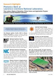
Research Highlights<strong>Photonics</strong> Work atLawrence Livermore National LaboratoryTony Ladran, Deputy <strong>of</strong> Operations, Photon Science and Applications Program,Lawrence Livermore National LaboratoryTHIS WORK PERFORMED UNDER THE AUSPICES OF THE U.S.DEPARTMENT OF ENERGY BY LAWRENCE LIVERMORE NATIONALLABORATORY UNDER CONTRACT DE-AC52-07NA27344The National Ignition Facility (NIF) & PhotonScience Directorate at Lawrence Livermore NationalLaboratory comprises five programs, each focused on oneor more aspects <strong>of</strong> NIF's missions. They are:National Ignition FacilityThe National Ignition Facility Project isresponsible for the construction and operation<strong>of</strong> NIF, a 192-beam experimental laserfacility. This unique facility is the world'slargest and highest-energy laser, capable <strong>of</strong> creating temperaturesand pressures similar to those that exist only in thecores <strong>of</strong> stars and giant planets and inside nuclear weapons.National Ignition CampaignThe National Ignition Campaign (NIC)encompasses all <strong>of</strong> the experiments, hardwareand infrastructure needed to carry outthe initial ignition experiments on NIF beginning in2010 and to continue research on ignition in the followingyears. NIC is a key element <strong>of</strong> the National NuclearSecurity Administration.Photon Science & ApplicationsThe Photon Science & Applications (PS&A)Program provides advanced solid-state laser andoptics technologies to the laboratory, government, and industry forimportant national needs. The primary activities <strong>of</strong> PS&A inrecent years have been: (1) to complete the laser technology ddevelopment and laser component testing for the U.S.Department <strong>of</strong> Energy's NIF project, (2) to develop advancedsolid-state laser systems and optical components for theDepartment <strong>of</strong> Defense and Department <strong>of</strong> Energy and (3) toaddress the needs <strong>of</strong> other government agencies and U.S. industry.Inertial Fusion EnergyThe Inertial Fusion Energy Program isexploring a variety <strong>of</strong> approaches to usinginertial confinement fusion, NIF's coretechnology to achieve energy gain and helplay the groundwork for the eventual use <strong>of</strong> fusion energyas a clean, safe, virtually limitless source <strong>of</strong> electricity.Science at the ExtremesNIF will become a premier internationalcenter for experimental science early in thenext decade. The extreme temperaturesand pressures that will be created insidethe NIF target chamber will enable scientists from aroundthe world to conduct unprecedented experiments in highenergy density science and to gain new insights into suchmysterious astrophysical phenomena as supernovae, giantplanets, and black holes.NIF: The ‘Crown Joule’ <strong>of</strong> Laser ScienceThe National Ignition Facility (NIF) is the world'slargest laser. See Figure 1. NIF's 192 intense laser beamswill deliver to its target more than 60 times the energy <strong>of</strong>any previous laser system. When all 192 beams are oper-Figure 1. Three football fields could fit inside the NIF Laser andTarget Area Building.4 <strong>IEEE</strong> LEOS NEWSLETTER <strong>June</strong> 2008
Accelerating the pace <strong>of</strong> engineering and scienceParlez-vousMATLAB?Over one million people aroundthe world speak MATLAB.Engineers and scientists in everyfield from aerospace andsemiconductors to biotech,financial services, and earth andocean sciences use it to expresstheir ideas.Do you speak MATLAB?Quantitative highthroughputgene expressionimaging using datafrom FlyEx Database.This example available atmathworks.com/ltc®©2007 The MathWorks, Inc.Image from FlyEx Database. Used by permission. http://flyex.ams.sunysb.edu/flyex and http://urchin.spbcas.ru/flyexThe language <strong>of</strong> technical computing.
ational in 2009, NIF will direct nearly two million joules<strong>of</strong> ultraviolet laser energy in billionth-<strong>of</strong>-a-second pulsesto the target chamber center.When all that energy slams into millimeter-sized targets,it can generate unprecedented temperatures andpressures in the target materials – temperatures <strong>of</strong> morethan 100 million degrees and pressures more than 100billion times Earth's atmosphere. These conditions aresimilar to those in the stars and the cores <strong>of</strong> giant planetsor in nuclear weapons; thus one <strong>of</strong> the NIF & PhotonScience Directorate's missions is to provide a betterunderstanding <strong>of</strong> the complex physics <strong>of</strong> nuclear weapons.Researchers can also explore basic science, such as astrophysicalphenomena, materials science and nuclear science.NIF's other major mission is to provide scientistswith the physics understanding necessary to create fusionignition and energy gain for future energy production.Figure 2. Technicians adjust the target positioner inside the NIFTarget Chamber.A Variety <strong>of</strong> ExperimentsNot all experiments on NIF need to produce fusion ignition.Researchers are planning many other types <strong>of</strong> experimentsthat will take advantage <strong>of</strong> NIF's tremendous energyand flexible geometry in non-ignition shots. Non-ignitionexperiments will use a variety <strong>of</strong> targets to derive abetter understanding <strong>of</strong> material properties under extremeconditions. These targets can be as simple as flat foils orconsiderably more complex. By varying the shock strength<strong>of</strong> the laser pulse, scientists can obtain equation-<strong>of</strong>-statedata that reveal how different materials perform underextreme conditions for stockpile stewardship and basic science.They also can examine hydrodynamics, which is thebehavior <strong>of</strong> fluids <strong>of</strong> unequal density as they mix.NIF experiments also will use some <strong>of</strong> the beams toilluminate "backlighter" targets to generate an X-rayflash. This allows detailed X-ray photographs, or radiographs,<strong>of</strong> the interiors <strong>of</strong> targets as the experimentsprogress. In addition, moving pictures <strong>of</strong> targets taken atone billion frames a second are possible using sophisticatedcameras mounted on the target chamber. These diagnosticscan freeze the motion <strong>of</strong> extremely hot, highlydynamic materials to see inside and understand the physicalprocesses taking place As construction <strong>of</strong> the 48"quads" <strong>of</strong> four beams each proceeded, many shots werealready being performed using the first quad <strong>of</strong> beams.Experiments beginning in the winter <strong>of</strong> 2007-2008 willtake advantage <strong>of</strong> additional quads as they come online.New Technologies Make NIF PossibleAmplifying NIF's beams to record-shattering energies,keeping the highly energetic beams focused, maintainingcleanliness all along the beam's path, and successfullyoperating this enormously complex facility – all requiredNIF's designers to make major advances in existing lasertechnology as well as to develop entirely new technologies.Innovations in the design, manufacture, and assembly<strong>of</strong> NIF's optics were especially critical.The Seven Wonders <strong>of</strong> NIFWhile construction <strong>of</strong> the football-stadium-sizedNational Ignition Facility was a marvel <strong>of</strong> engineering,NIF is also a tour de force <strong>of</strong> science and technologydevelopment. To put NIF on the path to ignition experimentsin 2010, scientists, engineers and technicians hadto overcome a daunting array <strong>of</strong> challenges.Working closely with industrial partners, the NIFteam found solutions for NIF's optics in rapid-growthcrystals, continuous-pour glass, optical coatings and newfinishing techniques that can withstand NIF's extremelyhigh energies. The team also worked with companies todevelop pulsed-power electronics, innovative control systemsand advanced manufacturing capabilities. Seventechnological breakthroughs in particular were essentialfor NIF to succeed:1.Faster, Less Expensive Laser Glass ProductionLaser glass is the heart<strong>of</strong> the NIF laser system;it's the material thatamplifies the laser lightto the very high energiesrequired for experiments.NIF's laserglass is a phosphateglass that contains achemical additive withatoms <strong>of</strong> neodymium.Figure 3. NIF Glass laser slab inproductionThe NIF laser system uses about 3,070 large plates <strong>of</strong>laser glass. Each glass plate is about three feet long andabout half as wide. If stacked end-to-end, the plateswould form a continuous ribbon <strong>of</strong> glass 1.5 miles long.To produce this glass quickly enough to meet constructionschedules, NIF uses a new production method developedin partnership with two companies – HoyaCorporation, USA and Schott Glass Technologies, Inc. –that continuously melts and pours the glass. See Figure3. Once cooled, the glass is cut into pieces that are polishedto the demanding NIF specifications.6 <strong>IEEE</strong> LEOS NEWSLETTER <strong>June</strong> 2008
2. Large Aperture Optical SwitchesA key element <strong>of</strong> the amplifier section<strong>of</strong> NIF's laser beampath is an opticaldevice called a plasma electrode Pockelscell, or PEPC, that contains a plate <strong>of</strong>potassium dihydrogen phosphate(KDP). See Figure 4. This device, inconcert with a polarizer, acts as a switch– allowing laser beams into the amplifierand then rotating its polarization totrap the laser beams in the amplifiersection. A thin plasma electrode that istransparent to the laser wavelength allows a high electric field tobe placed on the crystal, which causes the polarization to rotate.The trapped laser beams can then increase their energy muchmore efficiently using multiple passes back and forth throughthe energized amplifier glass. After the laser beams make fourpasses through the amplifiers, the optical switch rotates theirpolarization back to its normal configuration, letting themspeed along their path to the target chamber.3. Stable, High-Gain PreamplifiersNIF uses 48 preamplifiermodules, or PAMs,each <strong>of</strong> which provideslaser energy for fourNIF beams. The PAMreceives a very lowenergy (billionth <strong>of</strong> ajoule) pulse from themaster oscillator roomand amplifies the pulseby a factor <strong>of</strong> about amillion, to a millijoule. It then boosts the pulse onceagain to a maximum <strong>of</strong> about ten joules by passing thebeam four times through a flashlamp-pumped rod amplifier.To perform the range <strong>of</strong> experiments needed on NIF,the PAMs must perform three kinds <strong>of</strong> precision spatial,spectral and temporal shaping <strong>of</strong> the input laser beams.4. Deformable MirrorsThe deformable mirroris an adaptive optic thatuses an array <strong>of</strong> actuatorsto bend its surface tocompensate for wavefronterrors in the NIFlaser beams. There is onedeformable mirror foreach <strong>of</strong> NIF's 192beams. Advances inadaptive optics in theFigure 4. PlasmaElectrode Pockels CellFigure 5. 10 Joule PreAmpliermoduleFigure 6. 40 cm x 40 cm full aperturedeformable mirroratomic vapor laser isotope separation (AVLIS) program atLawrence Livermore National Laboratory demonstratedthat a deformable mirror could meet the NIF performancerequirement at a feasible cost. Livermore researchers developeda full-aperture (40-centimeter-square) deformablemirror that was installed on the Beamlet laser in early1997. Prototype mirrors from two vendors were also testedin the late 1990s. The first <strong>of</strong> NIF's deformable mirrorswere fabricated, assembled and tested at the University <strong>of</strong>Rochester's Laboratory for Laser Energetics and installedand successfully used on NIF to correct wavefronts for thefirst beams sent to target chamber center.5. Large, Rapid-Growth CrystalsNIF's KDP crystals servetwo functions: frequencyconversion and polarizationrotation. The development<strong>of</strong> the technologyto quickly grow highqualitycrystals shown inthis photo, were a majorundertaking and is perhapsthe most highlypublicized technologicalsuccess <strong>of</strong> the NIF project. NIF laser beams start out asinfrared light, but the interaction <strong>of</strong> the beams with thefusion target is much more favorable if the beams are ultraviolet.Passing the laser beams through plates cut from largeKDP crystals converts the frequency <strong>of</strong> their light to ultravioletbefore they strike the target. The rapid-growth processfor KDP, developed to keep up with NIF's aggressive constructionschedule, is amazingly effective: Crystals that wouldhave taken up to two years to grow by traditional techniquesnow take only two months. In addition, the size <strong>of</strong> the rapidgrowthcrystals is large enough that more plates can be cutfrom each crystal, so a smaller number <strong>of</strong> crystals can provideNIF with the same amount <strong>of</strong> KDP.6. Target FabricationTo meet the needs <strong>of</strong> NIFexperiments, NIF's millimeter-sizedtargetsmust be designed andfabricated to meet precisespecifications for density,concentricity and surfacesmoothness. When a newFigure 7. NIF rapid-growth KDPcrystalFigure 8. Target Assemblymaterial structure is needed, materials scientists create thenecessary raw materials. Fabrication engineers then determinewhether those materials – some never seen before – canbe machined and assembled. Manufacturing requirements forall NIF targets are extremely rigid. Components must bemachined to within an accuracy <strong>of</strong> one micrometer, or onemillionth<strong>of</strong> a meter. In addition, the extreme temperaturesand pressures the targets will encounter during experimentsmake the results highly susceptible to imperfections in fabrication.Thus, the margin <strong>of</strong> error for target assembly, whichvaries by component, is strict. Throughout the designprocess, engineers inspect the target materials and componentsusing nondestructive characterization methods toensure that target specifications are met and that all componentsare free <strong>of</strong> defects. Together, this multidisciplinary teamtakes an experimental target from concept to reality.8 <strong>IEEE</strong> LEOS NEWSLETTER <strong>June</strong> 2008
7. Integrated Computer Control SystemFulfilling NIF's promiserequires one <strong>of</strong> the mostsophisticated computercontrol systems in governmentservice or privateindustry. Every NIFexperimental shot requiresFigure 9. NIF Control Roomthe coordination <strong>of</strong> complex laser equipment. In theprocess, some 60,000 control points for electronic, highvoltage, optical and mechanical devices – such as motorizedmirrors and lenses, energy and power sensors, videocameras, laser amplifiers, pulse power and diagnosticinstruments – must be monitored and controlled. SeeFigure 9. The precise orchestration <strong>of</strong> these parts byNIF's integrated computer control system will result inthe propagation <strong>of</strong> 192 separate nanosecond (billionth <strong>of</strong>a second)-long bursts <strong>of</strong> light over a one-kilometer pathlength. The 192 separate beams must have optical pathlengthsequal to within nine millimeters so that thepulses can arrive within 30 picoseconds (trillionths <strong>of</strong> asecond) <strong>of</strong> each other at the center <strong>of</strong> a target chamberten meters in diameter. Then they must strike within 50micrometers <strong>of</strong> their assigned spot on a target measuringless than one centimeter long – an accuracy comparableto throwing a pitch over the strike zone from 350miles away.Developing the State-<strong>of</strong>-the-artfor National SecurityThe Photon Science and Applications (PS&A) program pursuesnational security missions by developing state-<strong>of</strong>-the-art opticsand laser technology. Through research and development,PS&A is developing technologies that advance the frontiers <strong>of</strong>diode-pumped laser technology, high-peak power lasers andscience, generation and application <strong>of</strong> bright, high-energy photonsand fabrication <strong>of</strong> precision, meter-scale optics.Tailored-Aperture Ceramic LaserTo improve the run time and beam quality <strong>of</strong> large, highaverage-power(HAP), diode-pumped solid-sate laser(DPSSL) systems, PS&A has developed a new slab laser technologycalled the tailored-aperture ceramic laser (TACL). Ahigher-performance descendent <strong>of</strong> the solid-state heat-capacityThe TACLLaser (SSHCL) system shown, TACL in Figure10 uses composite ceramic Nd3+:YAG/Sm3+:YAG slabsthat are edge pumped.By smoothing the high spatial frequency pump-deposition ripplesthat result from face pumping, edge pumping can improve systembeam quality and runtime considerably. New diode-pumparrays are also employed in TACL that use high-performancemicrolens conditioning and microchannel cooling. The microchannelcooling <strong>of</strong> the arrays allows the diode packages to be run with ahigh duty cycle – even continuously – while generating high averageoptical pump power. As a result, TACL designs can use as litx(−1)Figure 10. Edge pumping is made possible by use <strong>of</strong> a ceramic Sm3+:YAG frame that is integral to the Nd3+:YAG portion <strong>of</strong> the slab.Sm3+:YAG absorbs at the laser wavelength, but is transparent at the pump wavelength. The Sm3+:YAG frame suppresses amplified spontaneousemission without affecting passage <strong>of</strong> the pump light. This recent development proceeds from the concerted work <strong>of</strong> LLNL and theKonoshima Chemical Company and promises to revolutionize the design <strong>of</strong> large HAP laser systems by significantly improving beam quality.10 <strong>IEEE</strong> LEOS NEWSLETTER <strong>June</strong> 2008
tle as one-tenth <strong>of</strong> the diode arrays employed by the SSHCL systemwhile achieving the same power output capability.Solid-State Heat-Capacity LaserPS&A is developing a high-average-power (100-kW-class),diode-pumped, solid-state heat-capacity laser (SSHCL) suitable foruse in military weapons. A mobile, compact, and lightweightSSHCL laser system capable <strong>of</strong> being deployed on a variety <strong>of</strong> platformsis also under development. Potential military applications <strong>of</strong>such a system include the targeting and destruction <strong>of</strong> short-rangerockets, guided missiles, artillery and mortar fire, unmanned aerialvehicles and improvised explosive devices, or IEDs.In 2006, PS&A achieved a major accomplishment when theSSHCL produced 67 kilowatts <strong>of</strong> power – a 50 percent increase inthe world-record-setting power level achieved the previous year.See Figure 11. This class <strong>of</strong> power demonstrates that tabletop-sizedsolid-state lasers have come <strong>of</strong> age and can fulfill the performancerequirements for their use in tactical weapon applications.Additionally, improvements to the SSHCL's laser optics, bothin material selection and geometric architecture, have greatlyenhanced temperature pr<strong>of</strong>ile uniformity throughout the lasingcavity, yielding a beam quality two times the diffraction limit forfive seconds <strong>of</strong> run time in PS&A's unstable resonator. See Figure12. Beam quality control is integral to PS&A's laser systemdevelopment, and results like these portend the use <strong>of</strong> directedenergyweapons on the battlefield where they can effect "speed<strong>of</strong>-light"engagement in compact, mobile packages.The extremely high fracture toughness <strong>of</strong> ceramicYAG:Nd3+, along with its facility for use in composinglarger slabs, makes it the ideal material for laser gain media.Output Power (kW)806040200ReducedApertureThreeThree Four FiveNumber <strong>of</strong> SlabsCalculatedMeasured @10%Duty CycleMeasured @20%Duty CycleFigure 11. The 67 kilowatts <strong>of</strong> average power was achieved usingfive ceramic neodymium-doped yttrium aluminum garnet(YAG:Nd3+) laser-gain media slabs; model calculations were validatedby experimental results as depicted in the graph.Laser-Material InteractionPS&A's SSHCL test bed has afforded execution <strong>of</strong> extensivelaser-material interaction experiments using a wide variety<strong>of</strong> materials such as steels, aluminums, titaniums andorganic composites. Varying the spot size <strong>of</strong> the laser beamfrom a few millimeters to a 162-centimeter locus while sustainingan air flow rate <strong>of</strong> 100 meters per second at thepoint <strong>of</strong> laser-material interaction loosely simulates a targetflying in the atmosphere. See Figure 13. All tests were conductedat the nominal 25 kilowatts <strong>of</strong> average laser power.<strong>June</strong> 2008 <strong>IEEE</strong> LEOS NEWSLETTER 11
These test results reveal the functioning <strong>of</strong> several mechanismswhen the laser is used to destroy a target: thermalheating <strong>of</strong> the high explosive to ignition; increased materialremoval due to combustion <strong>of</strong> certain materials from the“Times Diffractioon Limited” BeamQuality8765432100Fall 2005Beam QualityFall 2005200 400 600 800 1000Shot Number (200 Shots = 1 Second)BK7 Window, No DiffusersFS Window, with Diffusers, Run #2Fused Silica Window, No Diffusers FS Window, with Diffusers, Run #3FS Window, with Diffusers, Run #1 FS Window, with Diffusers, Run #4Figure 13. SSHCL experimental test setup, using 25-kilowattaveragelaser power, 132-cm laser beam spot size, and 100-meterper-secondair flow.Figure 14. Concept <strong>of</strong> a 100-kW, movable, fully self-containedTACL/SSHCL ready for live target testing.Spring 2006No Diffusers, Power ~12 kW, with Diffusers, Power ! 10 kW, Unstable ResonatorFigure 12. A beam quality <strong>of</strong> two times the diffraction limit – for five seconds – wasachieved on the SSHCL testbed.increased oxygen during air flight; and aerodynamic forcesthat literally rip the membrane from the annealed andweakened target, making it aerodynamically unstable.Potential PlatformsThe development <strong>of</strong> a prototype platformusing SSHCL TACL technologysuitable for testing at a proving groundor test range is the next step in the evolution<strong>of</strong> directed-energy weapons. SeeFigure 14.The transition from a laser-technologydemonstration device in the laboratoryto a fully-operational, directedenergyweapon capable <strong>of</strong> engaging livetargets under battlefield conditions is akey PS&A objective.LLNL's work on the SSHCL heat capacityconcept has set the stage for a new generation<strong>of</strong> ceramic lasers and high-powerlaser architectures which will be capable <strong>of</strong>running continuously at high efficiencyand with exceptional beam quality.Diode-Pumped Alkali Laser:A New CombinationSince the advent <strong>of</strong> lasers more thanfour decades ago, solid-state and gaslasers have followed largely divergentdevelopment paths. Gas lasers are based primarily ondirect electrical discharge for pumping (energizing),while solid-state lasers are pumped by flashlamps andsemiconductor diode laser arrays.The alkali-vapor laser's intrinsically high efficiencyand its compatibility with today's commercially availablediode arrays enable fast-track development paths to tacticalsystems, with mass-to-power ratios that far exceedwhat is possible with today's other laser systems.Building on alkali-vapor laser research done by Z.Konefal, PS&A's Directed Energy Systems andTechnology (DEST) program element recently developeda new class <strong>of</strong> laser that combines features <strong>of</strong> both gas andsolid-state lasers, based on diode excitation <strong>of</strong> atomicalkali vapors. The defining features <strong>of</strong> the diode-pumpedalkali laser (DPAL) are its ability to be incoherentlypumped and its compatibility with diode arrays havingseveral-nanometer-wide spectral emissions. These characteristicsdistinguish DPALs from previous demonstrations<strong>of</strong> alkali-based lasers that used narrow-band, coherentpumping to demonstrate lasing.DEST's extensive laser modeling capability, anchored toexperimental laboratory demonstrations, supports extremepower scaling with good efficiency and beam quality.DEST is the world leader in the development <strong>of</strong> thisnew class <strong>of</strong> laser; the first demonstration took place atLawrence Livermore National Laboratory in 2002, seeFigure 15, and it has been followed by many otherdemonstrations and developments.12 <strong>IEEE</strong> LEOS NEWSLETTER <strong>June</strong> 2008
Fusion Energy Systems and ScienceFusion is the process by which the sun and stars produceenergy, and it is also responsible for much <strong>of</strong> the power <strong>of</strong>thermonuclear weapons. It also has the potential to be asource <strong>of</strong> unlimited, environmentally friendly energy forhumankind.The National Ignition Facility (NIF) is designed todemonstrate inertial confinement fusion, ICF, thatinvolves the rapid compression <strong>of</strong> small fuel capsules, asshown in figure 15, to reach densities and temperaturesgreater than those in the core <strong>of</strong> the sun; when a sufficientenergy density is reached, the fuel capsule ignites andthen burns while confined by its own inertia. NIF isexpected to demonstrate fusion ignition – the release <strong>of</strong>more energy via fusion burn than the laser energy used toinitiate ignition – early in the next decade, but will onlybe able to do so at a rate <strong>of</strong> one experiment every fewhours. For inertial fusion energy (IFE) production tobecome practical, targets will have to be ignited at a rate<strong>of</strong> several shots per second.The mission <strong>of</strong> the Fusion Energy Systems and Science(FESS) program element <strong>of</strong> PS&A is to develop the laserdriver technology necessary to make IFE production practical– including the development <strong>of</strong> low-cost, high-energy,high-efficiency laser drivers and components for repetitionrates <strong>of</strong> several times a second. Concurrent with thedevelopment <strong>of</strong> the National Ignition Facility is anotherambitious Livermore laser project named Mercury.The Mercury laser project is an important part <strong>of</strong> theFESS mission. It is designed to produce 100-joule pulsesat a ten-per-second repetition rate with one kilowatt <strong>of</strong>average power, using an architecture that could be scaledto IFE-relevant size. Mercury is a single-beam laser system,as shown in figure 16 that has developed capabilitiesthat will build on NIF's accomplishments. As currentlydesigned, NIF's 192 beams can fire simultaneously onlyonce every few hours. After each shot, the thousands <strong>of</strong>optics must be given a chance to cool down to ensure thatthey can operate correctly for the next shot.Mercury has developed a method <strong>of</strong> continuously coolingthe optics, while at the same time allowing the laserto fire rapidly over extended periods.The current technology propels high-velocity helium gasacross the optics to keep them cool, while laser pulses passthrough the optics at a sustained rate <strong>of</strong> ten shots a second.Unlike NIF, which uses seven-foot tall flashlamps toenergize the laser amplifiers, Mercury relies on diodelasers – similar to those in commercial read/write CDplayers – which give <strong>of</strong>f one-third as much heat as flashlamps.Mercury's beam is amplified as it passes throughslabs <strong>of</strong> specially grown ytterbium-strontium flouroapatitecrystals, as opposed to NIF's neodymium-dopedphosphate laser glass. More advanced amplifier media,such as transparent ceramics, are also being developed.As <strong>of</strong> mid-2008, Mercury has been able to run continuouslyfor several hours (300,000 shots), firing ten timesa second at more than 50 joules per shot, each shot lastingjust 15 nanoseconds (billionths <strong>of</strong> a second).The project, which beganin 1996 and was initiallyfunded through LLNL'sLaboratory Directed Researchand Development (LDRD)<strong>of</strong>fice, has already been awardedthree R&D 100 Awards,most recently for developing aunique frequency conversioncrystal. Earlier awards were forthe original design <strong>of</strong> Mercury'sdiode array and for its Pockelscell, a unique light-switchingtechnology.The long-term goal is alaser system capable producing<strong>of</strong> NIF's energy output,with Mercury's ability toFigure 15. NIF beam path intoa Hohlraumrapidly fire shots, and ignite inertial fusion targets forelectrical power generationHigh-Average-Power Laser-Diode ArraysFor 100-kW diode arrays to become a common reality, twoelements <strong>of</strong> the technology must be realized: high-performance,reliable diode bars, and heat sinks that can sustain superiorthermal management and precision-diode bar mounting.Figure 16. The Mercury laser system, a gas-cooled, diode-pumped, solidstatelaser, operates in a facility about the size <strong>of</strong> a handball court.<strong>June</strong> 2008 <strong>IEEE</strong> LEOS NEWSLETTER 13
Figure 17. The first demonstration<strong>of</strong> a resonance-transitionalkali laser using Rb vaporoccurred at LLNL in the winter<strong>of</strong> 2002.Lawrence Livermore NationalLaboratory (LLNL) has developedjust such a package fordiode bars, using silicon – themainstay <strong>of</strong> the semiconductorindustry.LLNL uses photolithographyand etching techniquesto produce tens <strong>of</strong>thousands <strong>of</strong> 30-μm-widechannels in silicon substratesthat carry coolingwater. The water flowingthrough these microchannelssignificantly cools the laser-diode bars, which aremounted on the silicon less than 200 μm from the channels.Combining ten diode bars onto a single heat sinkyields a ten-bar package (referred to as a "tile"), whichconstitutes the unit cell from which large, two-dimensionaldiode arrays can be built up through tiling.The tiles used to make up these large arrays shown inFigure 18 are called silicon monolithic microchannels(SiMMs). Considerations that drove the SiMM packagedesign included ease <strong>of</strong> fabrication and the ability to constructlarge laser-diode arrays with output power capabilities<strong>of</strong> ten to 100 kW. Of paramount importance in thedesign <strong>of</strong> the SiMM package was incorporation <strong>of</strong> thesame aggressive heat removal capability that characterizedLLNL's original, rack-and-stack silicon microchannel-cooledpackage. This was accomplished by placing themicrochannels into the silicon directly below the location<strong>of</strong> the attached laser-diode bars. Like the rack-and-stacksilicon microchannel cooler, the SiMM design maintains avery tight thermal circuit, with just 177 μm <strong>of</strong> siliconseparating the heat-generating laser-diode bars and themicrochannel fins that define the cooling channels.The SiMM laser-diode array is a packaging technology forproducing the smallest, most powerful and most inexpensivelaser-diode pumps ever. Each package <strong>of</strong> ten laser-diode barsintegrates the electrical, optical and hydraulic requirementsnecessary for high-average-power lasers. To date, arrays <strong>of</strong> up to100 kW have been fabricated at LLNL, and arrays <strong>of</strong> up to 100kW have been fabricated by SiMMtec, a commercial licensee <strong>of</strong>the technology.With the relatively low cost <strong>of</strong> silicon, large arrays <strong>of</strong>these precision microchannels can be fabricated inexpensivelyusing standard photolithography and etching techniques.Moreover, with silicon as the base material, individualdiode bars can be precisely soldered to a package;each laser diode bar is connected to an LLNL-patentedmicrolens, giving the SiMM package its unsurpassedoptical brightness.Silens FrameMicro LensLightOutputCuRibbonMetalNotchDiodeMicro-ChannelsWater InletGlassManifoldFigure 18. A 41-kW array made up <strong>of</strong> 28 SiMM packages. The sketch illustrates a portion <strong>of</strong> a SiMM laser-diode package.14 <strong>IEEE</strong> LEOS NEWSLETTER <strong>June</strong> 2008
Research HighlightsA Nanophotonic Interconnect for High-PerformanceMany-Core ComputationR. G. Beausoleil 1 , J. Ahn 2 , N. Binkert 2 , A. Davis 2 , D. Fattal 1 , M. Fiorentino 1 ,N. P. Jouppi 2 , M. McLaren 3 , C. M. Santori 1 , R. S. Schreiber 2 , S. M. Spillane 2 ,D. Vantrease 2 , and Q. Xu 11 INFORMATION AND QUANTUM SYSTEMS, HP LABORATORIES,1501 PAGE MILL RD., MS 1123, PALO ALTO, CA 94304–11232 EXASCALE COMPUTING, HP LABORATORIES,1501 PAGE MILL RD., MS 1177, PALO ALTO, CA 94304–11773 EXASCALE COMPUTING, HP LABORATORIES,FILTON ROAD, STOKE GIFFORD, BRISTOL BS34 8QZ, UKAbstractSilicon nanophotonics holds the promise <strong>of</strong> revolutionizing computingby enabling parallel architectures that combine unprecedentedperformance and ease <strong>of</strong> use with affordable power consumption.Here we describe the results <strong>of</strong> a detailed multiyeardesign study <strong>of</strong> dense wavelength division multiplexing (DWDM)on-chip and <strong>of</strong>f-chip interconnects and the device technologies thatcould improve computing performance by a factor <strong>of</strong> 20 aboveindustry projections over the next decade.1. IntroductionMoore’s Law is still a fundamental technology driver for the informationtechnology industry: the ITRS Semiconductor roadmap [1]shows, in the next decade and a half, a continued reduction in featuresizes from 40 nm to the sub-10-nm regime. This growth incircuit density has brought us into the multi-core CPU era, and weare on the eve <strong>of</strong> a many-core (16 or more cores per socket) era. Astransistor density increases, the number <strong>of</strong> transistors comprising asingle computer core is not growing; rather, it has pulled back forreasons <strong>of</strong> power efficiency, allowing the number <strong>of</strong> cores packagedon the die to grow exponentially. In the many-core era, on-chip and<strong>of</strong>f-chip communication are the critical issues for sustaining performancegrowth for the demanding, data-intensive applications forwhich these many-core chips are intended. Computational bandwidthscales linearly with the exponentially growing number <strong>of</strong>cores, but the rate at which data can be communicated across a chipusing top-level metal wires is increasing very slowly. The rate atwhich data can be communicated through pins at the chip edge isalso growing more slowly than the computational bandwidth, andthe energy cost <strong>of</strong> cross-chip and <strong>of</strong>f-chip (from processor socket toDRAM) communication significantly limits the achievable bandwidth.As a result, the field <strong>of</strong> computer architecture is now in a crisis.It is not clear that many-core processors will find widespreadDIMM 1 DIMM 2 DIMM CCPUMemory Controller 1Memory Controller 2Memory Controller CCore1Core2Core3Core4Core5Core6Core7Core8N = 4CCoreN−3CoreN−2CoreN−1CoreNCluster 1’s L2 CacheCluster 2’s L2 CacheCluster C’s L2 CacheOptical Crossbar/RingFigure 1: Schematic <strong>of</strong> the basic architecture for a 256-core processor. The cores are divided into clusters that share an L2 cache and controlaccess to a particular unit <strong>of</strong> memory.<strong>June</strong> 2008 <strong>IEEE</strong> LEOS NEWSLETTER 15
In Fig. 1, we show a block diagram <strong>of</strong> a many-core processorillustrating the basic idea behind the architecture considered here.The device is tiled with 64 identical four-core compute clusters,each <strong>of</strong> which has a memory controller that either interfaces tostacked memory or drives a photonic connection to <strong>of</strong>f-chip memoryto provide bandwidth that scales with processor performance.We interconnect the clusters with a photonic crossbar, <strong>of</strong>feringenormous bandwidth, modest latency, and very low power consumption.This creates a symmetric architecture in which all memoryis close to all processors; the programmer expresses parallelismat a high level, and is not burdened by issues <strong>of</strong> locality, therebygreatly reducing the difficulty <strong>of</strong> parallel program development.Furthermore, we can provide bandwidth <strong>of</strong> one byte per doubleprecisionfloating-point operation (flop) all the way to DRAM,eliminating the need to exploit very complex s<strong>of</strong>tware techniques(multilevel tiling, for example) to guarantee locality <strong>of</strong> reference.The bandwidth provided from DRAM is large enough to eliminatean entire layer <strong>of</strong> cache (L3), with significant savings in power andcost, while also reducing latency and hardware complexity.Energy efficiency is the primary motivation for many-core, andsmall, power-efficient cores and caches achieve the best possibleperformance per unit energy. We don’t anticipate significantincreases in CPU clock rates over the next decade, so we assume forour model that the cores use a 5 GHz clock. If we also assume thatthe cores are dual-issue, in-order, and multithreaded, and that they<strong>of</strong>fer SIMD instructions allowing 4 multiply-accumulate and 4-word-wide load/store operations, then the compute bandwidth <strong>of</strong>the device is 10 teraflops (i.e., double-precisionfloating-point operations per second),requiring (at one byte per flop) 20 TB/s <strong>of</strong>bidirectional interconnect bandwidth. Ourpower models predict that this processorwill dissipate approximately 200 W in thesilicon itself.3. The nanophotonic crossbarDespite the remarkable progress maderecently in broadband Mach-Zehnder electroopticmodulators [7] and quantum-wellmaterials for electroabsorption modulators[8,9], we believe that — in the long term —the use <strong>of</strong> dense wavelength-division multiplexing(DWDM) in optical interconnects isinevitable. In order to minimize the need forbuffering (and therefore eliminate the powerdissipated by serialization and deserialization,or SERDES), we assume that we will beable to drive each physical channel at twicethe clock frequency (i.e., read or write twobits per clock to/from digital registers), or 10Gb/s. Therefore, we will need 16,000 physicalchannels in our interconnect to supply therequired bidirectional bandwidth <strong>of</strong> 20 TB/s.However, in order to implement the crossbarwith the performance specifications (particularlylow latency) required by our architecture,we will need to avoid switching altogetherand overprovision the physical channelssignificantly. For example, in order to provide an all-to-all single-hopinterconnect topology, we will require total direct connectionsbetween the clusters. (In other words, at any given time, eachcluster may be sending data to only one <strong>of</strong> the other clusters, buteach cluster must always be connected physically to all 63 <strong>of</strong> theother clusters.) If we assume that we are using dies, and that eachwaveguide (or wire) occupies an area with dimensions 2 cm × 3 µmon average, we find that the interconnect will require over 200 layerson the die, which is clearly infeasible, regardless <strong>of</strong> whether weare using wires, direct optical modulation, or optical coarse wavelengthdivision multiplexing (CWDM). As we shall see next, usingDWDM in our design allows us to provide extraordinarily highinterconnectivity in only a single layer.As illustrated to scale in Fig. 2, one implementation <strong>of</strong> thenanophotonic crossbar employs 64 wavelengths multiplexed over270 parallel waveguides, with 256 waveguides allocated to controland data, 2 to broadcast, and 12 to arbitration. Each cluster “listens”to a single dedicated bundle <strong>of</strong> 4 waveguides, at all wavelengths.These 256 individual bit-wide channels are grouped intological channels for data and control messages. The timing <strong>of</strong> theselogical channels is synchronous, each channel being used by onesender to send to its destination in any given 24 clock “epoch.” Anew, distributed, all-optical crossbar arbitration scheme describedin Section 5 allocates the logical channels to sending clusters, allowingone sending cluster to transmit to a given destination cluster ina given epoch. Once granted permission by the arbiter to transmit,the sending cluster modulates all wavelengths on the allocatedCorning Incorporatedis a diversified technology companywith a rich history spanning morethan 150 years. Corning combinesour expertise in specialty glass,ceramic materials, polymers and themanipulation <strong>of</strong> properties <strong>of</strong> light withstrong process and manufacturingcapabilities to develop, engineer andcommercialize significant innovativeproducts for the flat panel display,telecommunications, environmentaland life sciences markets.We are seeking an applied scientist toconduct optical physics research andto provide expertise in fundamentalunderstanding <strong>of</strong> laser interactions withmaterials <strong>of</strong> fundamental importanceto Corning, including glasses andceramics. This position will also havethe opportunity to perform exploratoryresearch to extend our understanding<strong>of</strong> laser processing.Responsibilities:• Lead and/or support R&D teams todevelop laser process technologiesto enable next generation product orprocess features• Direct special investigations <strong>of</strong>laser system capabilities related toproduct or process performanceincluding laser output and laser/material interaction• Develop independent, exploratoryresearch efforts to characterizeand explore new laser/materialinteractionsRequired Skills:• Expertise in high power lasers andmaterial interaction (e.g. drilling,ablation, etc.)• Experimental experience with highpower lasers and optical beamdelivery systems• Ability to develop and leadindependent research effort tosupport laser processing initiativesEducation and Experience:• Ph.D. in physics, electricalengineering, materials science orrelated field• 5+ years experience with multipletypes <strong>of</strong> laser systems (UV, CO2,diode and/or Nd:YAG) includingbeam delivery systems.• 3+ years experience in field <strong>of</strong> laserprocessing <strong>of</strong> materialsSubmit your application online at:http://www.corning.com/careers/index.aspx and search ref #160941<strong>June</strong> 2008 <strong>IEEE</strong> LEOS NEWSLETTER 17
channel in order to send to the destination cluster. This on-chip,low-cost, high-bandwidth, low-power crossbar is able to handle asmany as 64 inputs and outputs simultaneously, and is a revolutionarydevelopment that will be significant in many applications; itenables the kind <strong>of</strong> flattened, symmetric architecture we desire.The same high bidirectional bandwidth to <strong>of</strong>f-stack memory isa requirement for our target performance. Even with the number <strong>of</strong>pins growing by 40 percent every generation, electrically-connectedmemory will in 2017 provide only one fifth <strong>of</strong> a byte per flop tothe processor. To fully exploit the advantages <strong>of</strong> optics, we reorganizememory into stacks with a photonic interface below the layers<strong>of</strong> DRAM, connected by fiber to the memory ports <strong>of</strong> the manycoreprocessor stack. This approach provides adequate bandwidth <strong>of</strong>about one byte per flop (and eventually even more if necessary),solving the chip-edge bandwidth problem. It does so while savingconsiderable power (up to 200 W if communicating at 10 TB/selectrically at 2.2 pJ/b). Optical interfaces enable asingle DRAMchip to source an entire cache line, making better use <strong>of</strong> the largeinternal DRAM memory bandwidth and reducing power even further.This will provide the bandwidth and power benefits <strong>of</strong> aprocessor-in-memory (PIM) architecture while keeping the programmability<strong>of</strong> a classical symmetric multiprocessor.4. Nanophotonic componentsThis ultra-high-bandwidth DWDM network is enabled by a number<strong>of</strong> CMOS-compatible nanophotonic devices that are (at most)only a few years beyond the current state <strong>of</strong> the art:1. Low-loss silicon-on-insulator (SOI) waveguides have measuredlosses as low as 0.2 dB/cm [10], and will not need muchimprovement. However, the commercially available SOI wafersused for this purpose today are custom-made to satisfy lightconfinement requirements by increasing the thickness <strong>of</strong> thetraditional oxide buffer layer, and are therefore relatively expensive.In addition, this thick oxide layer confines heat within thethin top silicon layer, which translates into a large temperaturebuild-up for sensitive resonant devices such as drop filters, modulators,and ring lasers. Therefore, in the long term, it will beimportant to develop means for creating nanophotonic componentsusing pure silicon wafers, which provide high thermalconductivity at low cost.2. Resonant receiver-less Ge detectors. The smaller bandgap <strong>of</strong>Ge than Si (0.7 eV vs. 1.1 eV) allows detection <strong>of</strong> opticalsignals in the 1300 nm wavelength range, and with properlydesigned material can likely extend to 1550 nm. Thepotential ability to fabricate Ge layers on Si <strong>of</strong>fers the possibility<strong>of</strong> integrating optical components with Si integratedcircuits for efficient electric-optical transduction. Ge canbe embedded into resonant detectors to allow a single wavelengthin a waveguide to be detected. This also enables lowcapacitancedetectors that eliminate the need for powerhungryamplifiers and clock recovery to build a receiver-lessdetection scheme [11].3. Resonant modulators. As described below, we propose to usering resonators that selectively modulate a single wavelengthon a given waveguide and can be moved to an “OFF” statewhere they are transparent to the data flux in the waveguide.The modulators work by changing the index <strong>of</strong> silicon ringsusing charge injection. Published results indicate that thetarget modulation rate <strong>of</strong> 10 Gb/s can be achieved with currenttechnology [12]. These rings will need to be kept resonantwith the chosen wavelength by thermal tuning <strong>of</strong> therefractive index.4. Multiwavelength lasers with precisely controlled frequencyintervals are ideal for low-cost DWDM systems. If only one <strong>of</strong>the frequency channels is servo-locked to an on-chip standardcavity, then all <strong>of</strong> the other frequency modes will track the controlledmode. One <strong>of</strong> the possible approaches is the Fabry-Perotcomb laser based on quantum dots [13], which has already beenused to demonstrate a bit-error-rate <strong>of</strong> at 10 Gb/s over ten longitudinalmodes [14,15]. Another possible approach is themode-locked hybrid Si/III-V evanescent laser [16], which uses asilicon-waveguide laser cavity wafer-bonded to a III-V gainregion. In this case, any ambient temperature change in theenvironment will cause approximately the same refractive indexshift in the laser cavity and the silicon waveguides and resonatorsthat form the DWDM network. Our design studyshows that the laser need only provide 1–2 W <strong>of</strong> total opticalpower to supply a 20 TB/s network if the detector capacitanceis low enough that only 30,000 photons are needed to drive a 1V swing at the detector’s output terminal.Acc.V Spot Magn Det WD Expμm3.00 kV 3.0 65000xTLD5.3 5 LSN#5 after etch1(a)Figure 3: (a) An SEM picture with 40°-tilted view <strong>of</strong> a microring resonator with a 1.5-µmradius coupled to a waveguide with an optimized (reduced) width. (b) A microscope picture<strong>of</strong> cascaded microring resonators coupled to a U-shaped waveguide at the edge <strong>of</strong> the chip.In our design <strong>of</strong> a single-layer DWDMnanophotonic interconnect, we have chosenthe silicon microring resonator as our foundationalcomponent because it has small size,high quality factor Q, transparency to <strong>of</strong>f-resonancelight, and no intrinsic reflections.Using injected charge, the refractive index <strong>of</strong>the microring can be changed, shifting thefundamental frequency <strong>of</strong> the cavity eitherinto or out <strong>of</strong> resonance with an incident lightfield. The microring can act as an optical filter[17,18], and it can be made into electroopticmodulators [12,19,20], lasers [21]and detectors when carrier injection, opticalgain, or optical absorption mechanisms areincorporated. In the past, the key characteristic<strong>of</strong> a silicon microring resonator yet to be18 <strong>IEEE</strong> LEOS NEWSLETTER <strong>June</strong> 2008(b)
EpochComponent Frequency1234Comp Bid Win12ML Laser Component 1Component 4Component 2Epoch 1Component Frequency1234Comp Bid Win12ML Laser Component 1Component 4Component 234Component 334Component 3(a)(b)Epoch 1Epoch 2ML Laser Component 1Component Frequency12341 42 43 24 1Component 4Component 3(c)Component 2Component Frequency1234Comp Bid Win Comp Bid Win1 42 33 44 1ML Laser Component 1Component 4Component 3(d)Component 2Figure 4: A simplified schematic example <strong>of</strong> an optical arbitration network used to provision four system resources. This scheme can runin parallel to (and independently from) the network used to transmit data between the cores. For example, each transmitter can determinewhether a particular target receiver is available without communicating with the receiver.demonstrated experimentally is a radius approaching the minimumpossible value that allows an intrinsic Q <strong>of</strong> 20,000, which is about1.4 µm. As shown in Fig. 3(a), we have fabricated Si microringswith radii <strong>of</strong> 1.5 µm [22] with intrinsic Qs <strong>of</strong> 18,000 and effectivemode volumes around 1.0 µm. When coupled to an optimallydesignedsilicon strip waveguide that minimizes spurious lightscattering and increases the critical dimensions <strong>of</strong> the geometry(easing fabrication requirements), the coupled Q approaches thetheoretical maximum possible value for a ring <strong>of</strong> that size (9,000out <strong>of</strong> 10,000). In Fig. 3(b), we show cascaded silicon microring resonatorsthat can be used as a modulator or filterbank in a nanophotonic network.In the case where we use the microring asa modulator, a small size is critical for severalreasons. First, a smaller size means that moremodulators can be fit into a given area, thereforeproviding higher integration density.Second and more importantly, the power consumption<strong>of</strong> the modulator, which is a keyperformance factor for electrooptical modulators,is directly proportional to the circumferenceand inversely proportional to the Q <strong>of</strong>the resonator. Reducing the size <strong>of</strong> the ringwithout sacrificing the Q is critical for lowpoweroperation. Third, the total bandwidth<strong>of</strong> a microring-based DWDM modulationsystem [20] is limited by the free spectralTechnology Node (nm)Clusters/chipCores/clusterComputational performance (Tflops)On-chip interconnectBi-directional bandwidth (TB/s)Power (W)Energy/bit (fJ)Off-chip interconnectBi-directional bandwidth (TB/s)Power (W)Energy/bit (fJ)range (FSR) <strong>of</strong> the microring resonator, which is inversely proportionalto the circumference <strong>of</strong> the ring. A smaller microring modulatorhas a larger FSR, which can therefore accommodate morewavelength channels and have higher aggregate data bandwidth. Inour case, the choice <strong>of</strong> a 1.5 µm radius and the demonstration <strong>of</strong> thenear-maximum-possible coupled Q <strong>of</strong> 9,000 provides a FSR <strong>of</strong>about 8 THz, and a filter bandwidth <strong>of</strong> about 20 GHz, which isnearly ideal for our interconnect architecture.One <strong>of</strong> the most important requirements that must be met bya nanophotonic interconnect is that its total thermal dissipation40 nm 28 nm 17 nm 14 nm4 16 64 644 4 4 160.64 2.56 10.24 40.961.28 5.12 20.48 81.923.4 18.0 38.4 118.4332 439 235 1811.28 5.12 20.48 81.921.8 4.3 8.9 27.5177 105 54 42TABLE 1: Projected DWDM interconnect performance at various technology nodes. Thepower consumption <strong>of</strong> the interconnect includes lasers and modulators, as well as the powerneeded to keep resonant detectors and modulators locked.<strong>June</strong> 2008 <strong>IEEE</strong> LEOS NEWSLETTER 19
emain below 25% that <strong>of</strong> the underlying silicon transistors, or lessthan 50 W for our target processor in 2017. As discussed above,we expect that the laser source will contribute about 5 W to thistotal, but the on- chip microrings will contribute a much largerquantity <strong>of</strong> heat. There are three possible modes for electricalpower dissipation in rings: fabrication error trimming, resonancefrequency biasing, and direct data modulation. Because <strong>of</strong> fabricationimperfections, each ring will have a resonance frequency thatis slightly different from the design goal, and must be “trimmed”into the correct spectral location. We can rely on two schemes t<strong>of</strong>ine-tune the rings: we can use carrier injection to blue-shift theresonance, and thermal heating to red-shift it. In the worst-casescenario we need 185 µW/nm to red-shift a 3-µm ring throughheating and 125 µW/nm to blue-shift it through current injection.The approach that combines heating and current injection,however, is only viable if the critical dimension control <strong>of</strong> the fabricationprocess is better than 1 nm. If this condition is not met,then thermal control alone needs to be used at the expense <strong>of</strong> amuch larger power consumption.The electric current required to modulate a ring is given byC/pulse at 5 GHz, or 30 fJ at 1 V, assuming that we detune the ring40 GHz from resonance to obtain an extinction ratio <strong>of</strong> 10 dB orgreater. This corresponds to a raw dissipated power <strong>of</strong> 150 µW peronline ring. However, the modulator voltage driver circuit will necessarilydissipate electrical power, since the modulator acts as acapacitive load with a 10 µA leakage current in the “on” state, andhas a peak current <strong>of</strong> 1 mA during the transition. Recently, thisproblem has been solved on-die by manufacturers <strong>of</strong> packagedCMOS photonic devices using AD-DA conversion drivers, but thepower dissipated in these drivers has been much greater than thepower expended in the modulators themselves. Therefore, in thelong term we believe that it will be important to develop purelyanalog CMOS drivers to reduce the electronic overhead by a factor<strong>of</strong> 30–100 over the current state-<strong>of</strong>-the art. We believe that the efficiency<strong>of</strong> these drivers will scale only slowly with circuit featuresize, resulting in a modulation power below 0.5 mW at the 17-nmtechnology node.Generally, in the reconfigurable network we will trim all rings(i.e., both modulators and detectors) away from resonance, andthen use current injection to bring the necessary rings online oncearbitration is complete. Given the silicon parameters mentionedabove, and that an active ring will be online during the entireepoch, the total power requirement per online ring is about 30µW, or about 0.1 mW including analog driver overhead at the 17-nm technology node. Therefore, in 2017 we expect the power dissipatedby all on-chip rings to be approximately 40 W. We haveBenchmarkOpticalPerfomanceElectricalPerformancemodeled the performance <strong>of</strong> the on-chip and <strong>of</strong>f-chip interconnectsshown in Fig. 2 at several technology nodes in Table 1. The totalpower consumption is the sum <strong>of</strong> the on-chip and <strong>of</strong>f-chip estimates,and includes all <strong>of</strong> the laser, modulation, and trimmingcontributions outlined above.ScaledOptical/ElectricalPTRANS (GB/S) 9102 459.0 22STREAM (GB/S) 10240 605.0 19GUPS 40 2.4 19DGEMM (Gflops) 37 37.0 1FFT (Gflops) 1734 879.0 2MPI (GB/s) 20 1.2 19TABLE 2: HPCS benchmark performance for the proposed architecture at the 17-nmtechnology node.5. All-optical arbitrationOne <strong>of</strong> the most significant contributions to the interconnect latencyis the time required to determine the availability <strong>of</strong> systemresources, arbitrate collisions between requests, and then grantaccess to the resource requestors. For example, in an all-to-all multihopswitched interconnect architecture (e.g., a torus), electricalsignals representing requests must be sent to an arbitration processor,and wait for the outcome <strong>of</strong> a computation and then receipt <strong>of</strong>another electrical signal before transmission can commence.However, a key advantage <strong>of</strong> our solution is that — at the cost <strong>of</strong>overprovisioning the nanophotonic components — the transmittersthemselves can reconfigure the crossbar in a few clock cycles,thus avoiding the need for hand-shaking procedures that increaselatency. Nevertheless, we still require an arbitration system to handlecollisions. The intrinsic parallelism <strong>of</strong> optical signals allows usto propose a novel, all-optical, low-latency arbitration system thatdoes not require digital electronic computation or communicationbetween the transmitter and receiver, using a protocol that can berun completely independently <strong>of</strong> the on-chip data network. Ouranalysis shows that this protocol provides nearly the best possiblethroughput under light and moderate loads, and about 90% <strong>of</strong> thebest possible throughput under heavy loads.A schematic diagram <strong>of</strong> a simple version <strong>of</strong> optical arbitration isshown in Fig. 4 for the case where there are four system resources(e.g., L2 caches in cores or clusters <strong>of</strong> cores) to be allocated. A fourwavelength(e.g., mode-locked) laser provides optical power to eachcomponent in a single distribution waveguide, and each wavelengthis dropped onto the arbitration waveguide at a specific locationin the ring. For example, the “red” wavelength (which in factmay belong to a particular channel near 1310 nm) is alwaysdropped onto the arbitration waveguide by a microring resonatornear component 1 that is always tuned to that wavelength. At thebeginning <strong>of</strong> the first 24-clock-cycle “epoch,” each resource isassigned a unique wavelength using a predetermined algorithmknown to each component, and each component prepares a “bid”for a particular resource (in this case, the right to transmit data toanother component). In an electrical arbitration system, this bidwould be an electrical signal sent to a dedicated subprocessor, buthere the bid is made locally by tuning an adjacent drop filter to thewavelength assigned to the desired target resource. For example,here component 1 bids for resource 4 by activating(i.e., tuning into precise resonance) alocal microring resonator that is designed todrop the wavelength currently assigned toresource 4 (i.e., “blue” during this epoch) ontoan integrated photodetector. If the opticalpower sensed by the photodetector rises abovea designated threshold, then component 1 haswon the right to transmit to resource 4.However, in this epoch, component 2 alsobids for access to resource 4; since component2 is “upstream” from component 1, and the20 <strong>IEEE</strong> LEOS NEWSLETTER <strong>June</strong> 2008
“blue” wavelength is dropped onto the arbitration waveguide nearcomponent 3, it is component 2 that wins the arbitration round andaccess to resource 4. Since the optical power at the “blue” wavelengthis removed from the waveguide by component 2, the “blue”photodetector sees a low optical intensity, and must wait until thenext epoch to try again to transmit data to resource 4. However,during the next epoch, the wavelengths representing the availableresources are reassigned, and now component 1 wins the right totransmit to resource 4 even though component 3 tries to bid for thesame resource. A more sophisticated token-ring optical arbitrationscheme [3] eliminates the need to synchronize execution duringepochs, and allows latency to be reduced even further.6. System performance modelsWe have modeled the performance <strong>of</strong> the nanophotonic architecturedescribed in the previous section (as well as an idealized electricalequivalent) for the HPC Challenge benchmarks [23], whichtypify high-performance data access patterns. In our model, we calculatedperformance limits due to CPU, interconnect, and memorybandwidths. We have assumed that the benchmarks have beenimplemented as multi-threaded shared-memory programs withdata imperfectly placed, requiring communication through the onchipinterconnect. We compare our nanophotonic architecture to amany-core electrically-interconnected alternative system, for whichwe assume an on-chip mesh network, power-limited to 50 W, andan electrical connection to memory with bandwidth limited by thepin count and pin bandwidth anticipated by ITRS in 2017. Ourestimated results for the 17 nm technologynode are shown in Table 2. The final columnlists the modeled ratio <strong>of</strong> optical performanceto electrical performance per unit <strong>of</strong> dissipatedheat. Note that four <strong>of</strong> the benchmarksshow a factor-<strong>of</strong>-20 improvement fornanophotonics over wires. The other twobenchmarks do not show significantimprovements because they are not bandwidthconstrained.build an all-optical arbitration system that relies on the samenanophotonic building blocks as the data-transmission network,allowing the transmitters themselves to determine whether areceiver is available, and to begin sending in only a few clock cycles.We have modeled the performance <strong>of</strong> this system using the HPCCbenchmarks, and we have found that a performance increase <strong>of</strong> 20over a purely electronic interconnect — essentially 4–5 “extra”Moore’s Law generations — is possible for applications that heavilyuse the interconnect. This extraordinary performance boost is acritical goal for those <strong>of</strong> us advocating such a radical departure fromcurrent semiconductor engineering practice: the transition to thisnew interconnect technology will be so painful for the IT industrythat only an order-<strong>of</strong>-magnitude improvement in compute bandwidthwill make the risk and effort worthwhile.References[1] http://www.itrs.net/.[2] R. G. Beausoleil, P. J. Kuekes, G. S. Snider, S.-Y. Wang, ,and R. S. Williams, “Nanoelectronic and NanophotonicInterconnect (Invited Paper),” Proc. <strong>IEEE</strong> 96, 230–247(2008).[3] D. Vantrease, R. Schreiber, M. Monchiero, M. McLaren, N.P. Jouppi, M. Fiorentino, A. Davis, N. Binkert, R. G.Beausoleil, and J. Ahn, “Corona: System Implications <strong>of</strong>Emerging Nanophotonic Technology,” in Proceedings <strong>of</strong> the35 International Symposium on Computer Architecture(ISCA 2008) (Beijing, China, 2008). To appear.7. ConclusionThe many-core architecture presented here— with the cores divided into silicon computeclusters, connected to each other and to<strong>of</strong>f-chip memory using nanophotonic technology— will continue to evolve [3] as wefurther explore the implications <strong>of</strong> a highlyparallel interconnect for the programmer.We believe that the use <strong>of</strong> DWDM in integrated-circuitinterconnects is inevitable,and that the optical components that wedescribe here are essential elements <strong>of</strong> thatapproach. The potentially high bandwidth <strong>of</strong>an optical interconnect in general-purposemany-core processors will be significantlycompromised if an electronically-reconfigurablecircuit-switched mesh or torus architecture[5] (essentially a photonic implementation<strong>of</strong> today’s copper-wire global interconnects)is employed. Instead, we propose to<strong>June</strong> 2008 <strong>IEEE</strong> LEOS NEWSLETTER 21
[4] N. Kirman, M. Kirman, R. K. Dokania, J. Martínez, A. B.Apsel, M. A. Watkins, and D. H. Albonesi, “OpticalTechnology in Future Bus-based Multicore Designs:Opportunities and Challenges,” <strong>IEEE</strong> Micro 27, 56–66(2007).[5] K. Bergman and L. Carloni, “Power efficient photonic networkson-chip,” in Proc. Soc. Photo-Opt. Instrum. Eng.,vol. 6898, p. 689813 (2008).[6] R. Ho, On Chip Wires: Scaling and Efficiency, Ph.D. thesis(2003).[7] W. M. Green, M. J. Rooks, L. Sekaric, and Y. A. Vlasov,“Ultra-compact, low RF power, 10 Gb/s silicon Mach-Zehnder modulator,” Opt. Express 15, 17106–17113(2007).[8] Y.-H. Kuo, Y.-K. Lee, Y. Ge, S. Ren, J. E. Roth, T. I.Kamins, D. A. B. Miller, and J. S. Harris, “Strong quantumconfinedStark effect in germanium quantum-well structureson silicon,” Nature 437, 1334–1336 (2005).[9] J. E. Roth, O. Fidaner, R. K. Schaevitz, Y.-H. Kuo, T. I.Kamins, J. S. Harris, and D. A. B. Miller, “Optical modulatoron silicon employing germanium quantum wells,” Opt.Express 15, 5851–5859 (2007).[10] A. Liu, R. Jones, L. Liao, D. Samara-Rubio, D. Rubin, O.Cohen, R. Nicolaescu, and M. J. Paniccia, “A high-speed siliconoptical modulator based on a metal-oxide-semiconductorcapacitor,” Nature 427, 615–618 (2004).[11] A. Bhatnagar, C. Debaes, H. Thienpont, and D. A. B.Miller, “Receiverless detection schemes for optical clock distribution,”in Proc. Soc. Photo-Opt. Instrum. Eng., vol.5359, pp. 352–359 (2004).[12] Q. Xu, B. Schmidt, S. Pradhan, and M. Lipson,“Micrometre-scale silicon electro-optic modulator,” Nature435, 325–327 (2005).[13] A. Kovsh, I. Krestnikov, D. Livshits, S. Mikhrin, J. Weimert,and A. Zhukov, “Quantum dot laser with 75nm broad spectrum<strong>of</strong> emission,” Opt. Lett. 32, 793–795 (2007).[14] A. Gubenko, I. Krestnikov, D. Livshtis, S. Mikhrin, A.Kovsh, L. West, C. Bornholdt, N. Grote, and A. Zhukov,“Error-free 10 Gbit/s transmission using individual Fabry-Perot modes <strong>of</strong> low-noise quantum-dot laser,” Electron. Lett.43, 1430–1431 (2007).[15] http://www.innolume.com/.[16] B. R. Koch, A. W. Fang, O. Cohen, and J. E. Bowers,“Mode-locked silicon evanescent lasers,” Opt. Express 15,11225–11233 (2007).[17] S. Xiao, M. H. Khan, H. Shen, and M. Qi, “A highlycompact third-order silicon microring add-dropfilter with a very large free spectral range, a flat passbandand a low delay dispersion,” Opt. Express 15,14765–14771 (2007).[18] M. S. Nawrocka, T. Liu, X. Wang, and R. R. Panepucci,“Tunable silicon microring resonator with wide free spectralrange,” Appl. Phys. Lett. 89, 071110 (2006).[19] Q. Xu, S. Manipatruni, B. Schmidt, J. Shakya, and M.Lipson, “12.5 Gbit/s carrier-injection-based silicon microringsilicon modulators,” Opt. Express 15, 430–436 (2006).[20] Q. Xu, B. Schmidt, J. Shakya, and M. Lipson,“Cascaded silicon micro-ring modulators for WDMoptical interconnection,” Opt. Express 14,9430–9435 (2006).[21] A. W. Fang, R. Jones, H. Park, O. Cohen, O. Raday, M. J.Paniccia, and J. E. Bowers, “Integrated AlGaInAs-siliconevanescent race track laser and photodetector,” Opt. Express15, 2315–2322 (2007).[22] Q. Xu, D. Fattal, and R. G. Beausoleil, “Silicon microringresonators with 1.5-µm radius,” Opt. Express 16,4309–4315 (2008).[23] http://icl.cs.utk.edu/hpcc/hpcc_results.cgi.Visit the LEOS web site formore information:www.i-LEOS.org22 <strong>IEEE</strong> LEOS NEWSLETTER <strong>June</strong> 2008
<strong>June</strong> 2008 <strong>IEEE</strong> LEOS NEWSLETTER 23
NewsCall for Nominations:The 2009 Tyndall AwardNominations are now being accepted for the 2009 TyndallAward, which will be presented at OFC/NFOEC 2009.This award, which is jointly sponsored by the <strong>IEEE</strong>Lasers and Electro-Optics <strong>Society</strong> and the Optical <strong>Society</strong> <strong>of</strong>America, is presented to a single individual who has madeoutstanding contributions in any area <strong>of</strong> lightwave technology,including optical fibers and cables, the optical componentsemployed in fiber systems, as well as the transmissionsystems employing fibers. With the expansion <strong>of</strong> this technology,many individuals have become worthy <strong>of</strong> consideration.The deadline for nominations is 10 August, 2008.For more information contact soc.leo@ieee.org orcheck the LEOS web for more details: www.i-leos.org –click “Awards” tab.Call for Nominations:2009 <strong>IEEE</strong>/LEOS Young Investigator AwardThe <strong>IEEE</strong> LEOS Young Investigator Award was establishedto honor an individual who has made outstanding technicalcontributions to photonics (broadly defined) prior to hisor her 35th birthday.The award shall consist <strong>of</strong> a certificate <strong>of</strong> recognitionand an honorarium <strong>of</strong> $1,000. The funding for this awardis being sponsored by General <strong>Photonics</strong> Corporation.Nomination packages will be due at the LEOS executive<strong>of</strong>fice by 30 September, 2008. Nominees must be under 35years <strong>of</strong> age on Sept. 30th <strong>of</strong> the year in which the nominationis made. The award may be presented either at theOptical Fiber Communications Conference (OFC), or theConference on Lasers and Electro-Optics (CLEO), to beselected by the recipient. The first award was CLEO 2007.Nomination packages consist <strong>of</strong> a nomination cover page, astatement <strong>of</strong> the nominee’s research achievements in photonics,the nominee’s curriculum vitae, and three to five reference letters(to be received at the LEOS <strong>of</strong>fice prior to the deadline).Please consider nominating an under-age-35 colleaguefor the inaugural cycle <strong>of</strong> this award!For full information about the LEOS awards programlook under the “Awards” tab on the LEOS web site(http://www.i-leos.org/)Nomination form can be found on page 26.Nominations for <strong>IEEE</strong> Medals and RecognitionsThe <strong>IEEE</strong> Awards Board is seeking nominations for <strong>IEEE</strong>Medals and Recognitions, and encourages the use <strong>of</strong> its onlinePotential Nominee Form. This form allows a preliminary review<strong>of</strong> a nominee by the selection committee and an opportunity toobtain feedback prior to submitting an <strong>of</strong>ficial nomination form.The Potential Nominee Form is available on the <strong>IEEE</strong>Awards Web Page at http://www.ieee.org/portal/pages/about/awards/noms/potnomform.html.The deadline for submission <strong>of</strong> an <strong>of</strong>ficial nomination formfor any <strong>of</strong> the <strong>IEEE</strong> Medals and Recognitions is 1 July,2008. For questions concerning the Potential NomineeForm, please contact awards@ieee.org.24 <strong>IEEE</strong> LEOS NEWSLETTER <strong>June</strong> 2008
News (cont’d)<strong>June</strong> 2008 <strong>IEEE</strong> LEOS NEWSLETTER 25
News (cont’d)26 <strong>IEEE</strong> LEOS NEWSLETTER <strong>June</strong> 2008
News (cont’d)<strong>IEEE</strong> Fellow First Woman Honoredwith John Fritz MedalDr. Kristina M. Johnson, provost andsenior vice president for AcademicAffairs at Johns Hopkins University,recently received the John Fritz Medalfrom the American Association <strong>of</strong>Engineering Societies (AAES). She is thefirst woman so honored. Johnson wasone <strong>of</strong> seven honorees during the AAES29th annual awards ceremony in theGreat Hall <strong>of</strong> the National Academy <strong>of</strong>Engineering on 5 May. She was cited forher internationally acknowledgedexpertise in optics, optoelectronicswitching and display technology.The John Fritz Medal, referred to asthe highest award in the engineeringpr<strong>of</strong>ession, is presented each year for scientificor industrial achievement in anyfield <strong>of</strong> pure or applied science. It wasestablished in 1902 as a memorial to thegreat engineer whose name it bears. Pastrecipients include Alexander GrahamBell (1907), Thomas Edison (1908),Alfred Nobel (1910), Orville Wright(1920) and Guglielmo Marconi (1923).Johnson is an <strong>IEEE</strong> Fellow, LEOSmember, and Electrical Engineer who, asthe former dean <strong>of</strong> engineering at DukeUniversity, increased the engineeringfaculty by 50 percent, tripled the size <strong>of</strong>the teaching and research facilities, andtripled the number <strong>of</strong> women engineeringfaculty, many in leadership positions.She co-founded the Colorado AdvancedTechnology Institute for Excellence inOptoelectronics and started several companiesthat are commercially successfulin color projection devices and intellectualproperty licensing.President’s Column(continued from page 3)The changes introduced this year in thePhAST program directly address the maingoal through all <strong>of</strong> the objectives, but particularlythrough objectives 3 and 4.PhAST is strongly focused on applicationsthat are market driven (so addressingobjective 3), with a program intended topresent the latest technologies and thecontext in which they are deployed inapplications.Addressing objective 4 is more challenging.In practice, increased co-operation withother disciplines implies developing relationshipswith other societies, a process thattakes time. LEOS is at the center <strong>of</strong> a number<strong>of</strong> ‘joined up’ networks <strong>of</strong> societies.These networks include communications,displays, nanotechnology, biotechnologyand biometrics, some <strong>of</strong> which have operatedsuccessfully for many years, with others,emerging only recently emerged.CLEO/QELS/PhAST falls in the former categoryand is owned and run by three cosponsoringsocieties: LEOS, OSA and APS.The OIDA is involved in developing aspects<strong>of</strong> the PhAST program for the first time.The OIDA involvement is bringing acompletely new perspective to PhASTthrough the Business Development sessions.These sessions are aimed at developing anunderstanding <strong>of</strong> the entire product valuechain, and developing roadmaps for the relevantindustries going forward. This isbeing achieved through a mixture <strong>of</strong> presentationsby senior managers and technologistsfollowed by interactive panel sessionsto develop further the ideas that emergeduring the presentations.The OIDA part <strong>of</strong> the program is furthermorefocused on the emerging area <strong>of</strong>‘green’ photonics. As well as resonatingwith the interests <strong>of</strong> LEOS, this also forms alink with <strong>IEEE</strong> as a whole, which hasdeclared sustainable technologies a priorityarea. It is becoming clear that the photonicsindustry will provide many solutions forreducing environmental pollution and theworld’s carbon footprint. These solutionsinclude highly efficient solid-state lighting,effluent-free laser processing, new low energydisplay technologies and photovoltaicenergy generation.Other key parts <strong>of</strong> the program includethe Power Lunch, organized by MiltonChang, and the PhAST/Laser Focus WorldInnovation Awards.PhAST raises a number <strong>of</strong> questions forLEOS. The principal question is how readilythe format could be used elsewhere. LEOSis already working with OIDA to exploreextending the concept <strong>of</strong> matching technicaland business sessions in a single workshop.LEOS is also actively working with other<strong>IEEE</strong> societies to identify more applicationsfocusedtopics that use photonics. A secondpoint is that this year’s PhAST sessions areentirely invited, which is appropriate forcertain meetings but clearly imposes limitson member participation. A third point isthat there is no charge to attend PhAST.Many attendees will have registered forCLEO/QELS, but an intention <strong>of</strong> PhAST isto support the CLEO Exhibition by attractingwalk-ins. Clearly having no registrationfee is not an option for independent events.My belief is that we can develop a model toaddress applications focused topics thatcombines the LEOS core values <strong>of</strong> volunteerservice, education, integrity, technical rigorand inclusiveness, and at the same time issustainable.All <strong>of</strong> these questions will be addressedby LEOS over the coming months. The ultimateaim <strong>of</strong> LEOS is to serve its membersand the photonics community. Moving intomore areas <strong>of</strong> application is one way <strong>of</strong>addressing this aim and I would welcomeyour views on how this can best be achieved.Finally, I would like to remind you <strong>of</strong> theappeal I made in January where I invitedyou to recruit one new member each in2008. As the middle <strong>of</strong> the year approaches,LEOS membership has started to grow forthe first time in several years. This is excellentnews, but there is still much that couldbe done. The best recommendation is a personalone – if you value LEOS membership,please spread the message to your colleaguesand build a stronger LEOS community.
News (cont’d)Memoriam: Pr<strong>of</strong>essor Pak Lim Chu12 November 1940 – 15 March 2008Pr<strong>of</strong>. Chu at the City University <strong>of</strong>Hong KongThe fiber-optics community haslost a great icon with the passing<strong>of</strong> Pr<strong>of</strong>. Pak Chu after a one yearbattle with cancer. His passing wascommemorated with an extendedservice <strong>of</strong> thanksgiving, eulogy,tributes, and valediction at theWest Sydney Chinese ChristianChurch that was attended by anoverflowing congregation <strong>of</strong> colleagues,friends, and fellowChristians.Pr<strong>of</strong>. Chu is a great championand a pioneer in the field <strong>of</strong> fiberoptics in Australia. He set up thevery first academic fiber-opticsresearch laboratory in Australia atthe University <strong>of</strong> New South Wales(UNSW) in 1970s. The laboratorywas equipped with the first preform-makingand fiber-drawingfacilities in the country. For thelast 30 years, Pr<strong>of</strong>. Chu has madeextensive contributions to theoptical fiber technology. In early1980s, he invented an acclaimedmethod to measure the refractiveindexpr<strong>of</strong>iles <strong>of</strong> fiber preforms.The method was adopted in anadvanced commercial instrumentfor the characterization <strong>of</strong> opticalfibers. In the mid-1980s, he successfullysolved the problem <strong>of</strong>soliton interaction, which laid animportant foundation for solitoncommunications, a field in whichhe maintained an interest for over20 years. In addition, Pr<strong>of</strong>. Chuhad worked on a large number <strong>of</strong>innovative optical devices, includingnonlinear optical switches,fiber-optic acoustic sensors, polymerfiber Bragg gratings, and verticaloptical polymer waveguidecouplers. This work has attractedconsiderable attention over theyears. His study on chaos communicationsis also very influential. Inrecent years, he spent much effortin promoting polymer optical fibertechnology, a growing field withmany potential applications inshort-distance transmission andoptical sensing. His contributionsto the field <strong>of</strong> fiber optics areinvaluable.On the teaching side, Pr<strong>of</strong>. Chusupervised over 40 doctoral andnumerous honours students anddeveloped the first undergraduatecourses in optical communicationstechnology in Australia.Pr<strong>of</strong>. Chu was a popular speaker,particularly at meetings inSoutheast Asia, giving numerouscontributed and invited talks aswell as short courses and tutorials.He was a Fellow <strong>of</strong> several scientificsocieties including the AustralianTechnological <strong>Society</strong> and theOptical <strong>Society</strong> <strong>of</strong> America. Hepublished almost 500 journal andconference papers, and was honouredin 2001 with the CentenaryMedal <strong>of</strong> Australia for his contributionto optical communications.In 2001, Pr<strong>of</strong>. Chu retired fromUNSW and moved to the CityUniversity <strong>of</strong> Hong Kong (CityU)where he became Pr<strong>of</strong>essor andDirector <strong>of</strong> the OptoelectronicsResearch Centre (RCO). During hisDirectorship <strong>of</strong> RCO, he made significantcontributions to the development<strong>of</strong> the photonics researchprograms at CityU. His cheerful,positive, and supportive temperamentenabled him to be an excellentmentor and a real friend <strong>of</strong>many people. Pr<strong>of</strong>. Chu was alsoactive in fostering collaborationswith industry and organising internationalconferences and trainingworkshops to raise the pr<strong>of</strong>ile <strong>of</strong> thephotonics community in HongKong. After his retirement fromCityU in 2006, he joined a localcompany, LINKZ InternationalLimited (the former NetworkingCable Business Unit <strong>of</strong> LTK),where he continued to make contributionsin photonics for the rest <strong>of</strong>his time in Hong Kong.Pr<strong>of</strong>. Chu is survived by his wifeEva, daughter Evelyn, son Desmondand five grandchildren.Optoelectronics Group,Department <strong>of</strong> ElectronicEngineering,City University <strong>of</strong> Hong Kong,April 200828 <strong>IEEE</strong> LEOS NEWSLETTER <strong>June</strong> 2008
Career Section2008 <strong>IEEE</strong>/LEOS Quantum Electronics AwardRecipients: Jeffrey H. Shapiro and Horace P. YuenThe Quantum Electronics Award isgiven to honor an individual (orgroup <strong>of</strong> individuals) for outstandingtechnical contributions to quantumelectronics, either in fundamentals orapplication or both. The Award maybe for a single contribution or for adistinguished series <strong>of</strong> contributionsover a long period <strong>of</strong> time. No candidateshall have previously received amajor <strong>IEEE</strong> award for the same work.Candidates need not be members <strong>of</strong>the <strong>IEEE</strong> or LEOS. The deadline fornominations is 16 February.Jeffrey H.ShapiroJeffrey H. Shapirois Director <strong>of</strong> theResearch Laboratory<strong>of</strong> Electronics (RLE)at the MassachusettsInstitute <strong>of</strong> Technology(MIT). Hereceived the S.B.,S.M., E.E., andPh.D. degrees inElectrical Engineering from MIT in1967, 1968, 1969, and 1970, respectively.As a graduate student he was aNational Science Foundation Fellow, aTeaching Assistant, and a Fannie andJohn Hertz Foundation Fellow. Hisdoctoral research was a theoreticalstudy <strong>of</strong> adaptive techniques forimproved optical communicationthrough atmospheric turbulence.From 1970 to 1973, Dr. Shapirowas an Assistant Pr<strong>of</strong>essor <strong>of</strong>Electrical Sciences and AppliedPhysics at Case Western ReserveUniversity. From 1973 to 1985, hewas an Associate Pr<strong>of</strong>essor <strong>of</strong>Electrical Engineering at MIT, and in1985, he was promoted to Pr<strong>of</strong>essor<strong>of</strong> Electrical Engineering.From 1989 until 1999 Dr. Shapiroserved as Associate Department Head<strong>of</strong> MIT's Department <strong>of</strong> ElectricalEngineering and Computer Science.In 1999 he became the Julius A.Stratton Pr<strong>of</strong>essor <strong>of</strong> ElectricalEngineering. In 2001, Dr. Shapirowas appointed Director <strong>of</strong> RLE.Dr. Shapiro's research interestshave centered on the application <strong>of</strong>communication theory to optical systems.He is best known for his workon the generation, detection, andapplication <strong>of</strong> squeezed-state lightbeams, but he has also publishedextensively in the areas <strong>of</strong> atmosphericoptical communication, coherentlaser radar, and quantum informationscience.Dr. Shapiro is a fellow <strong>of</strong> theInstitute <strong>of</strong> Electrical and ElectronicsEngineers, <strong>of</strong> the Optical <strong>Society</strong> <strong>of</strong>America, <strong>of</strong> the American Physical<strong>Society</strong>, and <strong>of</strong> the Institute <strong>of</strong> Physics,and he is a member <strong>of</strong> SPIE (TheInternational <strong>Society</strong> for OpticalEngineering). He has been an AssociateEditor <strong>of</strong> the <strong>IEEE</strong> Transactions onInformation Theory and the Journal <strong>of</strong>the Optical <strong>Society</strong> <strong>of</strong> America, and wasthe Principal Organizer <strong>of</strong> the SixthInternational Conference on QuantumCommunication, Measurement andComputing (QCMC'02). He currentlyco-chairs the Steering Committee forthe International Conferences onQuantum Communication, Measurementand Computing, and is Co-Director <strong>of</strong> the W. M. KeckFoundation Center for ExtremeQuantum Information Theory.Horace P. Yuen is aPr<strong>of</strong>essor <strong>of</strong> ElectricalEngineering andComputer Scienceand Pr<strong>of</strong>essor <strong>of</strong>Physics and Astronomyat NorthwesternUniversity.Horace P. YuenHe received hisdegrees in Electrical Engineering fromMassachusetts Institute <strong>of</strong> Technology.His technical research interests aremainly in the areas <strong>of</strong> communicationand cryptography, especially thosewith quantum effects. He is a recipient<strong>of</strong> the first International QuantumCommunication Award presented byTamagawa University <strong>of</strong> Japan, a fellow<strong>of</strong> the American Physical <strong>Society</strong>,and a senior member <strong>of</strong> <strong>IEEE</strong>. Several <strong>of</strong>his papers are collected in various specialvolumes, including "One HundredYears <strong>of</strong> Physical Review," which waspublished by the American Physical<strong>Society</strong> in 1993.<strong>June</strong> 2008 <strong>IEEE</strong> LEOS NEWSLETTER 29
Career Section (cont’d)2008-09 Distinguished Lecturers:The Distinguished Lecturer Awards are presented to honor interesting speakers who have made recent significant contributionsto the field <strong>of</strong> lasers and electro-optics. The Distinguished Lecturers speak at LEOS Chapters worldwide. Please contact you localchapter to see when one <strong>of</strong> the Lecturers will be speaking in your area. A list <strong>of</strong> current LEOS Chapter Chairs is available on theLEOS web site (www.i-LEOS.org).This year’s new Lecturers are:John C. Cartledge, Queen’s University, Ontario, CanadaTopic <strong>of</strong> Lecture: Optical and Electronic Signal Processing for Fiber-Optic CommunicationsJohn M. Dudley, Laboratoire d’Optique P.M. Duffieux, FranceTopic <strong>of</strong> Lecture: Nonlinear Fiber Optics and Supercontinuum Generation: New Fibers, New OpportunitiesPrem Kumar, Northwestern University, IL, USATopic <strong>of</strong> Lecture: Fiber-Optic Quantum Communications and Information ProcessingLecturers serving a second term are:Weng Chow, Sandia National Laboratory, NM, USATopic <strong>of</strong> Lecture: Many-Body Effects and Their Influences on Semiconductor LasersSilvano Donati, Universita Pavia, ItalyTopic <strong>of</strong> Lecture: Coupling in Lasers and Applications to Self-Mixing Interferometry and Chaotic CryptographyEl-Hang Lee, INHA University, South KoreaTopic <strong>of</strong> Lecture: Optical Printed Circuit Board (O-PCB) and VLSI <strong>Photonics</strong>Colin McKinstrie, Bell Labs, Alcatel-Lucent, NJ, USATopic <strong>of</strong> Lecture: Optical Signal Processing by Parametric DevicesCun-Zheng Ning, Arizona State University, AZ, USATopic <strong>of</strong> Lecture: Nanolasers Based on Semiconductor Nanowires and Surface Plasmons2008-2009 LEOS Distinguished LecturersJohn C. Cartledge was a Member <strong>of</strong>the Scientific Staff at Bell-NorthernResearch, Ottawa, Ontario, Canada,from 1979 to 1982, where his workinvolved fiber-optic systems for theexchange access network and highcapacitydigital radio systems. Since1982 he has been with theDepartment <strong>of</strong> Electrical andComputer Engineering, Queen'sUniversity. In July 2002 he was appointed an inauguralrecipient <strong>of</strong> a Queen’s Research Chair. He has spent one-yearsabbatical leaves with the Lightwave Systems TechnologyResearch Division <strong>of</strong> Bellcore, Red Bank, NJ, in 1988-89,and with the Optical Communications Department <strong>of</strong> TeleDanmark Research, Hørsholm, Denmark in 1995-96. Dr.Cartledge has served as a consultant and instructor in thearea <strong>of</strong> lightwave technology to several organizations. Hiscurrent research interests include optical modulators, opticalsignal processing (wavelength converters, optical regenerators),electronic signal processing for arbitrary opticalwaveform generation, and dispersion compensating fiberBragg gratings. Dr. Cartledge is Chair <strong>of</strong> the OpticalNetworks and Systems Committee, <strong>IEEE</strong> Lasers and30 <strong>IEEE</strong> LEOS NEWSLETTER <strong>June</strong> 2008
Career Section (cont’d)Electro-Optics <strong>Society</strong>, 2007-2009, and is a Fellow <strong>of</strong> theOptical <strong>Society</strong> <strong>of</strong> America.Dr. Cartledge’s conference organization activitiesinclude serving on the Technical Program Committees forthe Conference on Optical Fiber Communications (1994-1997 and 2005-2006), the <strong>IEEE</strong> LEOS Annual Meeting(2002-2008), the European Conference on OpticalCommunications (2006-2008), and the joint meeting <strong>of</strong>the International Conference on Integrated Optics andOptical Fibre Communications and the EuropeanConference on Optical Communications (1997). He was aProgram Chair for the joint meeting <strong>of</strong> the Conference onOptical Fiber Communications and the National FiberOptics Engineers Conference (2008).Title <strong>of</strong> Talk: Optical and Electronic Signal Processing forFiber-Optic CommunicationsCurrently, there is a substantial research and developmenteffort directed toward optical signal processing andelectronic signal processing for fiber-optic communications.Much <strong>of</strong> the work is aimed at mitigating theeffects <strong>of</strong> transmission impairments such as chromaticdispersion, polarization mode dispersion, fiber nonlinearities,amplifier noise, and band-limiting. It is beingpursued in the presence <strong>of</strong> an ongoing interest in increasingthe per-channel bit rate in order to meet the growingdemand for telecommunication services. For opticalsignal processing, a variety <strong>of</strong> approaches are availablefor implementing functions such as 3R (re-amplification,reshaping and re-timing) regeneration. For electronicsignal processing, advanced digital signal processingis being applied to both fiber-optic transmitters andreceivers, and has lead to a renewed interest in coherentoptical detection. This lecture presents an overview <strong>of</strong>optical and electronic signal processing technologies,including a critical assessment <strong>of</strong> each approach. Specificexamples are considered in more detail to highlight keyaspects <strong>of</strong> the technologies.John Dudley received B.Sc andPh.D. degrees from the University<strong>of</strong> Auckland in 1987 and 1992respectively. In 1992 and 1993, hecarried out postdoctoral researchat the University <strong>of</strong> St Andrews inScotland before taking a lecturingposition in 1994 at the University<strong>of</strong> Auckland. In 2000, he wasappointed Pr<strong>of</strong>essor at theUniversity <strong>of</strong> Franche-Comté in Besançon, France,where he currently heads the Optoelectronics and<strong>Photonics</strong> research group. He was named a member <strong>of</strong>the Institut Universitaire de France in 2005, and electeda Fellow <strong>of</strong> the Optical <strong>Society</strong> <strong>of</strong> America and aSenior Member <strong>of</strong> the <strong>IEEE</strong> in 2007. He serves on theEditorial boards <strong>of</strong> Optics Express, Optical andQuantum Electronics and Optical Fiber Technology. Heis General Chair <strong>of</strong> CLEO Europe 2009 and currentlyserves as the secretary <strong>of</strong> the Quantum Electronics andOptics Division <strong>of</strong> the European Physical <strong>Society</strong>.Title <strong>of</strong> Talk: Nonlinear Fiber Optics and SupercontinuumGeneration: New Fibers, New OpportunitiesResearch in nonlinear fiber optics is currently undergoingdramatic expansion, motivated by advances anddevelopments in new classes <strong>of</strong> optical fiber and theready availability <strong>of</strong> a wide range <strong>of</strong> optical pumpsources. This lecture will survey selected recent work inthis field that has investigated novel nonlinear propagationeffects in both photonic crystal and highly nonlinearoptical fibers, and will focus particular attention onthe physics and applications <strong>of</strong> supercontinuum generation.The lecture will provide both a tutorial review <strong>of</strong>the basic supercontinuum generation broadening mechanismsas well as a discussion <strong>of</strong> recent developmentsand applications.Prem Kumar is the AT&TPr<strong>of</strong>essor <strong>of</strong> Information Technologyin the department <strong>of</strong> ElectricalEngineering and Computer Scienceand Director <strong>of</strong> the Center forPhotonic Communication andComputing in the McCormickSchool <strong>of</strong> Engineering and AppliedScience at Northwestern University.He also holds an appointment asPr<strong>of</strong>essor <strong>of</strong> Physics and Astronomy and joinedNorthwestern in 1986 after spending five years at MIT asa research scientist. He received a Ph.D. in Physics fromthe State University <strong>of</strong> New York at Buffalo in 1980. Heis the author or co-author <strong>of</strong> over 400 publications,including one edited book, six patents, over 140 papers inpeer-reviewed journals, 40 articles in hard-bound volumes,and over 80 invited conference papers. His researchfocuses on the development <strong>of</strong> novel free-space and fiberopticdevices for ultrahigh-speed optical and quantumcommunication networks. He is a fellow <strong>of</strong> the Optical<strong>Society</strong> <strong>of</strong> America (OSA), a fellow <strong>of</strong> the AmericanPhysical <strong>Society</strong> (APS), a fellow <strong>of</strong> the Institute <strong>of</strong>Electrical and Electronic Engineers (<strong>IEEE</strong>), and a fellow <strong>of</strong>the Institute <strong>of</strong> Physics, UK (IoP). In 2006 he received theMartin E. and Gertrude G. Walder Research ExcellenceAward from Northwestern University and in 2004 he was<strong>June</strong> 2008 <strong>IEEE</strong> LEOS NEWSLETTER 31
Career Section (cont’d)the recipient <strong>of</strong> the 5th International QuantumCommunication Award established by the TamagawaUniversity in Tokyo, Japan. On the academic side, his pr<strong>of</strong>essionalservices have included Associate Editor, OpticsLetters; General (Program) Co-Chair, QELS 2008(2006); Principal Organizer, 4th InternationalConference on Quantum Communication, Measurement,and Computing, 1998. On the business side, he is thefounder <strong>of</strong> NuCrypt LLC, a startup company focusing onthe commercialization <strong>of</strong> quantum encryption technologyfor securing the physical layer <strong>of</strong> fiber-optic and free-spaceoptical networks.Title <strong>of</strong> Talk: Fiber-Optic Quantum Communications andInformation ProcessingRecognizing the ubiquitous standard optical fiberfor long-distance transmission and the widespreadavailability <strong>of</strong> efficient active and passive fiber devices,there are significant efforts underway to develop practicalresources for quantum communications and informationprocessing in optical fiber networks.Entanglement, which refers to the nonclassical dependency<strong>of</strong> physically separated quantum systems, is onesuch resource that is essential for implementing many<strong>of</strong> the novel functions <strong>of</strong> quantum information processing.Therefore, the efficient generation and distribution<strong>of</strong> quantum entanglement in fiber optical systemsis <strong>of</strong> prime importance. Entanglement has been historicallyproduced by use <strong>of</strong> the spontaneous parametricdown-conversion process in second-order nonlinearcrystals, wherein one higher-frequency pump photonsplits into two lower-frequency daughter photonswhich can be entangled. Coupling such down-convertedphotons into optical fibers without degradingentanglement, however, has remained a challengingtask. Fortunately, the prospects for ready availability <strong>of</strong>entanglement in the telecom band have dramaticallyimproved in the last few years by the emergence <strong>of</strong> anew technique for generating entanglement directly inthe fiber itself. This technique utilizes the Kerr nonlinearity<strong>of</strong> standard optical fiber to produce quantumcorrelated photons through the spontaneous four-wavemixing process. The correlated photons can be entangledin various ways by incorporating indistinguishablepathways in the four-wave mixing amplitude. In thislecture, I will review the status <strong>of</strong> this field by describingrecent experiments that demonstrate the generationand distribution <strong>of</strong> quantum entanglement is wavedivisionmultiplexed optical fiber systems. I will alsopresent some recent results on utilizing such entanglementfor quantum communications and informationprocessing tasks.Weng Chow received the Ph.D.degree in physics from the University<strong>of</strong> Arizona. His dissertation workinvolved fluctuation phenomena inquantum optics. At present, he isDistinguished Member <strong>of</strong> theTechnical Staff at Sandia NationalLaboratories. Weng Chows primaryresearch interest is in the application<strong>of</strong> microscopic theory to semiconductorlaser device development. Some <strong>of</strong> this work is described intwo texts, Semiconductor-Laser Physics and Semiconductor-Laser Fundamentals: Physics <strong>of</strong> the Gain Materials. His otherinterests include laser gyros, phased arrays, coupled lasers, quantumoptics and optical ignition <strong>of</strong> pyrotechnics.Weng Chow also holds the positions <strong>of</strong> Research Pr<strong>of</strong>essor <strong>of</strong>Physics at Texas A&M University, Adjoint Pr<strong>of</strong>essor <strong>of</strong> OpticalSciences at the University <strong>of</strong> Arizona and Honorary Pr<strong>of</strong>essor <strong>of</strong>Physics at Cardiff University. He has served on the CLEO semiconductorlaser program committee and is an associate editor <strong>of</strong><strong>IEEE</strong> Journal <strong>of</strong> Quantum Electronics. Weng Chow is a fellow<strong>of</strong> the Optical <strong>Society</strong> <strong>of</strong> America, and recipient <strong>of</strong> the Dept <strong>of</strong>Energy, Basic Energy Science/Material Science Award, theAlexander von Humboldt Senior Scientist Award and the LEOSDistinguished Lecturer Award.Talk title: Many-Body Effects and Their Influences onSemiconductor LasersThe incorporation <strong>of</strong> many-body effects into semiconductorlasergain calculations has led to significant improvement inaccuracy and predictive capability. This talk will explain themany-body effects and sketch the formulation <strong>of</strong> a laser theorycontaining the necessary physics. Examples <strong>of</strong> application <strong>of</strong> thetheory will be presented. These examples involve laser systemsranging from VCSELs to wide-bandgap and quantum-dot lasers.S. Donati is full Pr<strong>of</strong>essor atUniversity <strong>of</strong> Pavia since 1980. Heauthored 2 books (Photodetectors,Prentice Hall 1999, and ElectroopticalInstrumentation, PrenticeHall 2004), about 250 papers inJournal and Conference Proceedings,and has been the Guest Editor <strong>of</strong> adozen Special <strong>Issue</strong>s (JSTQE, JoO-A,Opt.Engineer., JQE, etc.). His seminalpapers on self-mixing interferometry and opticalchaotic cryptography have totaled 500+ citations. He is aFellow <strong>of</strong> <strong>IEEE</strong> and <strong>of</strong> OSA. Has founded and has beenthe Chair <strong>of</strong> the LEOS Italian Chapter. Has been LEOSVP Region 8 membership and BoG member <strong>of</strong> the LEOS.He is presently the Chair <strong>of</strong> the <strong>IEEE</strong> Italy Section.32 <strong>IEEE</strong> LEOS NEWSLETTER <strong>June</strong> 2008
Career Section (cont’d)Title <strong>of</strong> talk: Coupling in Lasers and Applications toSelf-Mixing Interferometry and Chaotic CryptographyIn this presentation, we start with a brief theoretical introductionto mutual and self coupling phenomena in laser oscillator,and then describe in details two applications. The firstis self-mixing interferometry for measurements <strong>of</strong> displacement,distance, vibration, and angle, and physical parameterslike coupling factors, line width, alfa-factor. In this case, thelaser undergoes self-injection at weak level, leading to anamplitude and frequency modulation driven by external opticalpath. The second application is optical chaos, which is generatedby the laser source at strong level <strong>of</strong> injection. Wedescribe mutual and self-injection generation <strong>of</strong> chaos, and thefirst step <strong>of</strong> development to cryptography, that is, synchronization.Then, we will review several schemes <strong>of</strong> coding anddecoding <strong>of</strong> information, i.e., chaotic masking and CSK (chaosshift keying) and how they can be implemented, along withtheoretical and experimental results carried out recently.El-Hang Lee obtained his B.S.E.E.(summa cum laude), at SeoulNational University, Korea, 1970;M.S., M.Phil., and Ph.D., AppliedPhysics, at Yale University, 1973,1975 and 1977, respectively, underPr<strong>of</strong>. John. B. Fenn (Yale NobelLaureate, Chemistry, 2002) andPr<strong>of</strong>. Richard. K. Chang (HenryFord II Pr<strong>of</strong>essor, former student <strong>of</strong>Pr<strong>of</strong>. N. Bloembergen, Harvard Nobel Laureate, Physics,1981). He conducted teaching, research and management atYale, Princeton, MEMC, AT&T Bell, ETRI (vice president),KAIST, and at INHA in the fields <strong>of</strong> semiconductorphysics, materials, devices, optoelectronics, photonics, andoptical communication. Founding Dean, School <strong>of</strong>Communication and Information Engineering; Dean,Graduate School <strong>of</strong> the Information Technology andTelecommunications; Founding Director, OPERA (Opticsand <strong>Photonics</strong> Elite Research Academy) and m-PARC(micro/nano-<strong>Photonics</strong> Advanced Research Center); VicePresident, Optical <strong>Society</strong> <strong>of</strong> Korea; Founding President,<strong>IEEE</strong>-LEOS Korea; Founding Director, SPIE-Korea. 230international refereed SCI-covered journal and reviewpapers; 640 international conference presentations; 100 plenary,keynote, and invited talks in international conferences;Edited books and international proceedings; 120international patents; 100 services as international conferencechair, committee member, and advisor. Fellow, <strong>IEEE</strong>(USA), IEE (UK), OSA (USA), SPIE (USA), APS (USA),KPS (Korea), IEEK (Korea), and Life Fellow, KoreanAcademy <strong>of</strong> Science and Technology. Recipient <strong>of</strong> 15national and international awards, including PresidentialMedal <strong>of</strong> Honor (Science), Korea; King Sejong Award(Science), Korea; <strong>IEEE</strong>/LEOS Chapter-<strong>of</strong>-the-Year Award,and the <strong>IEEE</strong> Third Millennium Medal, USA.Title <strong>of</strong> Talk: Optical Printed Circuit Board (O-PCB) andVLSI <strong>Photonics</strong>This lecture presents a comprehensive review andoverview on the cutting-edge frontier science andengineering <strong>of</strong> micro/nano-photonic integration thatwe have been pursuing aiming for what we call “opticalprinted circuit boards” (O-PCBs) and VLSI photonicchips. It discusses on the theory, design, fabrication,and integration <strong>of</strong> micro/nano-scale photonicdevices, circuits, and networks in the form <strong>of</strong> “VLSIphotonic integrated circuits” (VLSI-PICs) and “opticalmicro/nano-networks (O-MNNs)” <strong>of</strong> generic andapplication-specific nature on O-PCB platforms.These systems are designed to be compact, highspeed,light-weight, low-powered, low-cost, intelligent,and environmentally friendly as applicable fordatacom, telecom, transportation, aero-space, avionics,bio/medical, sensor, and environmental systems.The O-PCBs, VLSI-PICs and O-MNNs process opticalsignals through optical wires, devices, and circuits incontrast to the traditional electrical PCBs, VLSI-ICs,and networks. The O-PCBs and VLSI photonic systemsare to overcome the limitations <strong>of</strong> the electricalPCBs and VLSI-IC systems and are also aimed to integrateconvergent IT/BT/NT micro/nano-devices, circuits,and chips for broad based applications andusages. The new optical systems consist <strong>of</strong> 2-dimensionalplanar arrays <strong>of</strong> optical wires, circuits anddevices <strong>of</strong> micro/nano-scale to perform the functions<strong>of</strong> sensing, storing, transporting, processing, switching,routing and distributing optical signals on flatmodular boards or chips. The integrated optical componentsinclude micro/nano-scale light sources, waveguides,detectors, switches, modulators, sensors,directional couplers, multi-mode interference devices,AWGs, wavelength filters, micro-ring resonatordevices, photonic crystal devices, plasmonic devices,and quantum devices, made <strong>of</strong> polymer, silicon andother semiconductor materials. The lecture discussesscientific and technological issues, challenges, andprogresses regarding the miniaturization, interconnectionand integration <strong>of</strong> micro/nano-scale photonicdevices, circuits, and networks leading to ultra-smalland very large scale integration and discusses theirpotential applications. The issues include the diversecompatibility issues between micro/nano-devices suchas materials mismatch, size mismatch, shape mismatch,mode mismatch, optical mismatch, mechani-<strong>June</strong> 2008 <strong>IEEE</strong> LEOS NEWSLETTER 33
Career Section (cont’d)cal/thermal mismatch and the micro/nano-opticaleffects such as micro-cavity effects, non-linear effects,and quantum optical effects in small devices. Scalingrules for the miniaturization and integration <strong>of</strong> themicro/nano-photonic systems will also be discussed incomparison with those <strong>of</strong> the electrical systems. Newphysics, new materials, new designs, and new visions,issues and challenges <strong>of</strong> the optical micro/nano-opticalcircuits, networks and systems will be discussed alongwith the historical perspectives <strong>of</strong> the electrical technology.Recent progresses and examples will be presentedalong with the future outlook.Colin J. McKinstrie receivedBSc and PhD degrees from theUniversities <strong>of</strong> Glasgow andRochester, in 1981 and 1986,respectively. From 1985 to 1988he was a Postdoctoral Fellow <strong>of</strong>Los Alamos National Laboratory,where he was associated with theApplied Physics Division andthe Center for NonlinearStudies. In 1988 he returned to the University <strong>of</strong>Rochester as a Pr<strong>of</strong>essor <strong>of</strong> Mechanical Engineering anda Scientist in the Laboratory for Laser Energetics, wherehis main research interests were plasma-based particleacceleration, laser-plasma interactions and nonlinearfiber optics. Since 2001 Dr. McKinstrie has been aMember <strong>of</strong> the Technical Staff at Bell Laboratories,where his research concerns the amplification andtransmission <strong>of</strong> optical pulses in communication systems.He has served on technical committees for CLEO,FiO, LEOS and OFC, and is the Chair <strong>of</strong> the OSAQuantum Electronics Division.Title <strong>of</strong> Talk: Optical Signal Processing by ParametricDevicesParametric devices based on four-wave mixing infibers provide many functions that are required byoptical communication systems. When operated in thelinear regime, parametric devices provide amplification,frequency conversion and phase conjugation, allwith high gain levels and broad bandwidths. They canalso be used to buffer, monitor and switch optical signals.When operated in the nonlinear regime, parametricdevices regenerate signals. They also produceentangled and squeezed states <strong>of</strong> light. In this talkrecent research on parametric devices will bereviewed, and the implications <strong>of</strong> this research forclassical and quantal communication systems will bediscussedCun-Zheng Ning obtained hisPhD in Physics from University<strong>of</strong> Stuttgart. He was a SeniorScientist, group leader, or taskmanager at NASA Ames Centerfor Nanotechnology, NASAAmes Research Center from1997-2006. He joined ArizonaState University in 2006, wherehe is a Pr<strong>of</strong>essor <strong>of</strong> ElectricalEngineering with the Center for Nanophotonics,Arizona Institute <strong>of</strong> NanoElectronics, and AffiliatePr<strong>of</strong>essor in Materials and in Physics. Dr. Ning hasbeen conducting research in the general fields <strong>of</strong> laserphysics, semiconductor lasers, optoelectronic devicemodeling and simulation for the last 20 years.Recently, he has also developed a significant experimentalprogram in semiconductor nanowire researchon nanowire growth, optical characterization, anddevice fabrication. His group was the first to growantimonide nanowires and first to demonstrate a single-nanowireinfrared laser. His group has also beenactively engaged in semiconductor plasmonic devicesfocusing on integrating semiconductor nanostructureswith metallic nanostructures for various applicationssuch as nanolasers, solar cells and detectors. He haspublished 120 scientific papers and given many conferencepresentations including ~50 invited talks. Hehas served in many international conference committeesincluding SPIE <strong>Photonics</strong> West, OSA annualmeetings, and CLEO. He also served in editorial committeeor as a special topic editor for a few journalsincluding <strong>IEEE</strong> JQE, J. Special. Topics in QuantumElectron., J. Opt. Soc. Am., Optics Express, etc. Forhis research at NASA, he was winner <strong>of</strong> many NASAand NASA contractor awards.Title <strong>of</strong> Talk: Nanolasers Based on Semiconductor Nanowiresand Surface PlasmonsThe pursuit <strong>of</strong> nanotechnology in general and miniaturization<strong>of</strong> electronic devices in particular have seriously challengedthe optoelectronics community to develop ever smaller lasersand optoelectronic devices compatible with the trend in microelectronics.Vertical-cavity surface emitting lasers measured afew microns were once the smallest lasers. The situation is nowrapidly changing over the last 5 years with the demonstration <strong>of</strong>lasing capability <strong>of</strong> a single semiconductor nanowire <strong>of</strong> ~ 100nanometers in diameter. The question <strong>of</strong> great importance is:what is the ultimate size limit <strong>of</strong> a laser?To answer this and related questions, my lecture willstart with impressive recent progress in growth, fabrication,and characterization <strong>of</strong> semiconductor nanowires and34 <strong>IEEE</strong> LEOS NEWSLETTER <strong>June</strong> 2008
Career Section (cont’d)demonstration <strong>of</strong> lasing activities in various wavelengths.These lasers represent the smallest lasers <strong>of</strong> any kind atpresent. We will show how this new type <strong>of</strong> miniaturizedlasers differs from the conventional semiconductor lasers.To further reduce the dimension <strong>of</strong> nanowire lasers, arecent proposal <strong>of</strong> using metal coating <strong>of</strong> semiconductorwires will be evaluated. We will show that a proper design<strong>of</strong> a metal coated semiconductor nanowire can achieve lasingthreshold despite significant metal loss. Very recentexperimental results <strong>of</strong> demonstrating such lasers will bepresented. Finally some recent novel ideas involving surfaceplasmonic excitations at metal-semiconductor interfacewill be discussed where much smaller lasers could bepotentially made, with size independent <strong>of</strong> wavelengths.Membership SectionBenefits <strong>of</strong> <strong>IEEE</strong> Senior MembershipThere are many benefits to becoming an <strong>IEEE</strong> Senior Member:• The pr<strong>of</strong>essional recognition <strong>of</strong> your peers for technical and pr<strong>of</strong>essional excellence• An attractive fine wood and bronze engraved Senior Member plaque to proudly display.• Up to $25 gift certificate toward one new <strong>Society</strong> membership.• A letter <strong>of</strong> commendation to your employer on the achievement <strong>of</strong> Senior member grade(upon the request <strong>of</strong> the newly elected Senior Member.)• Announcement <strong>of</strong> elevation in Section/<strong>Society</strong> and/or local newsletters, newspapers and notices.• Eligibility to hold executive <strong>IEEE</strong> volunteer positions.• Can serve as Reference for Senior Member applicants.• Invited to be on the panel to review Senior Member applications.The requirements to qualify for Senior Member elevation are, a candidate shall be an engineer, scientist, educator, technical executiveor originator in <strong>IEEE</strong>-designated fields. The candidate shall have been in pr<strong>of</strong>essional practice for at least ten years and shall haveshown significant performance over a period <strong>of</strong> at least five <strong>of</strong> those years.”To apply, the Senior Member application form is available in 3 formats: Online, downloadable, and electronic version. Formore information or to apply for Senior Membership, please see the <strong>IEEE</strong> Senior Member Program website:http://www.ieee.org/organizations/rab/md/smprogram.htmlNew Senior MembersThe following individuals were elevated to Senior Membership Grade thru March-May:Timothy J. CarrigChing K. ChiaMarc P. ChristensenDennis DericksonGlen P. DudevoirChang-Hee LeeMark S. LeesonYiu-Wing LeungAnhui LiangAlexander S. LogginovSergei A. MalyshevShahid MasudPhyllis R. NelsonJesper NorregaardDaniel L. PettersonAleksandar D. RakicJae-Hyun RyouMasatoshi SaruwatariHrayr A. SayadianMichael A. SeiglerJulian B. SooleBarton W. StuckAnna TzanakTimo AaltoGuido ChiarettiR. P. DahlgrenDavid L. EsquibelSarath D. GunapalaLawrence A. HornakJianjang HuangShafiqul IslamBoero L. PaoloYuan ShiJoseph J. TalghaderYuelin WangYong-Gang Zhang<strong>June</strong> 2008 <strong>IEEE</strong> LEOS NEWSLETTER 35
Membership Section (cont’d)LEOS Central New England Chapter (CNEC)The 2007-08 academic year has beenanother busy year for the Central NewEngland Chapter <strong>of</strong> LEOS, colloquiallyknown as the Boston Chapter. Asthe oldest local LEOS Chapter in the<strong>IEEE</strong>, as well as one <strong>of</strong> its largest in acompact geographical area, with over300 local active members, we strive tomeet the high standards set by themany previous generations <strong>of</strong> pastlocal chapter chairs. To this end, wemaintain our chapter’s two strong traditions<strong>of</strong> holding 10 monthly technicalseminars (Sept. – <strong>June</strong>) on currentresearch topics in Lasers/Optics withtruly outstanding speakers (see listbelow), and putting on a 10 speakertutorial Workshop on a single current“hot” topic, with 2 speakers per nighton 5 consecutive Wednesday nights(see list below) in the spring or fall.This year the workshop subject chosenwas Plasmonics, which followedour previous years workshops onTerahertz Systems, Nanophotonics,and Photonic Crystals. We requirepre-registration for our yearly workshop,and generally charge a minimalfee (e.g. $50 for all 5 nights) to coverthe cost <strong>of</strong> refreshments during thebreaks and printing <strong>of</strong> the handouts.Each year the number registering forour local workshop has increased, hitting115 for this year’s fall PlasmonicsWorkshop. Equally rewarding, is thatwe are now receiving requests fromspeakers asking to give a talk at ourlocal yearly workshop once the topicis announced. This year we had toinclude a third speaker on one night,as it is just getting harder and harderto down-select from the abundance <strong>of</strong>appropriate well-qualified speakersavailable.Otherwise, on the mechanics <strong>of</strong>running our chapter, we find thatmost <strong>of</strong> our yearly changes are more inthe category <strong>of</strong> fine-tuning, to betterrespond to our changing member’sneeds, although we did make permanentthe two major changes we institutedlast year. First, we had movedour monthly meeting location to MITLincoln Laboratories in suburbanBoston, after alternatively meeting inthe old suburban Verizon / GTE Labsfor over 20 years (Verizon afterabsorbing GTE closed its labs andsold the land to a developer), and atBoston University in downtownBoston (BU began charging for parkingat evening meetings). But, perhapseven this change might not befinal, as MIT Lincoln Laboratories ison Government property, we learnedthat we had no possible appeal, whenin December an approaching snowstormled <strong>of</strong>ficials to close the buildingwe meet in, only hours before ourmeeting began. Second, we movedour meeting time to earlier in theevening and now serve free pizza ands<strong>of</strong>t drinks during the networkinghour before our monthly meetings.This was done because we learned,while being continuously re-educatedover the past 25 years that our industrialmembers will not drive intodowntown Boston traffic to pay forparking at a University location, thatfree pizza always attracts graduatestudents to our meetings at such alocation. Thus, we developed a hybridapproach to serve/attract at least part<strong>of</strong> the available student audience. Byserving pizza during the hourbetween when the MIT Lincoln Labworkday ends, and our monthly meetingstarts, some <strong>of</strong> the large number<strong>of</strong> MIT graduate students doing theirdaily research at Lincoln Lab delaytheir return to Cambridge for a couple<strong>of</strong> hours, to eat pizza, talk with us,and attend our meeting, before catchingthe last buses back to Cambridgeat 7:30 PM. Hopefully, those that stayin the Boston area after graduationwill continue to attend our meetings.Already, a couple <strong>of</strong> recently graduated,new-hire Lincoln Lab staff members,who volunteered to help run ourchapter, have greatly decreased theaverage age <strong>of</strong> our chapter <strong>of</strong>ficers.In addition, we have also workeddiligently on maintaining, whatmight be thought <strong>of</strong> as a rather overambitiousadvertising campaign bythose from outside <strong>of</strong> the suburbanBoston area, <strong>of</strong> our monthly chaptermeetings and Workshops to promoteattendance. But, as we have learnedfrom much past bitter experience, weare competing with all the daily seminarsand departmental colloquiums <strong>of</strong>over 25 world-class Universities andColleges in the Boston/Cambridgearea, with their world-wide draw <strong>of</strong>technical speakers from every fieldin Physics, Engineering, andBiology. These day-time talks saturatethe market for technical informationfor anyone associated with aUniversity, College, or academicresearch institution in the city.While the downside is that it isvery hard to convince an audience<strong>of</strong> faculty members and researchersworking in the Boston/Cambridgearea that we can produce bettertalks in their respective field at ourevening chapter meeting, theupside is that we have the widestand deepest collection <strong>of</strong> talentfrom which to draw local speakers(we find that even out-<strong>of</strong>-countryspeakers, talking at a universityduring the day, are willing to giveanother talk that evening at thelocal LEOS chapter meeting).Hence, it is critical for us to designthe advertising for our chaptertalks to reach other audiences,which are mostly drawn from localindustry surrounding suburbanBoston, rather than from theresearch establishment at theBoston/Cambridge Universities.36 <strong>IEEE</strong> LEOS NEWSLETTER <strong>June</strong> 2008
Membership Section (cont’d)We reach our intended audience byutilizing the <strong>IEEE</strong> Boston Section/CNEC newsmagazine “The Reflector”,in both paper and electronic formats(paid circulation over 13,000 in easternMass, NH, Maine and RI), and on ourown Web site ,as well as the local <strong>IEEE</strong>Web site . Inaddition we distribute at the Septemberand January LEOS meetings, and bymail to the local Universities, Colleges,and Government and CorporateResearch Labs, a one page poster <strong>of</strong> allthe upcoming fall or spring talk’s Titlesand Speakers. An electronic <strong>PDF</strong> copy<strong>of</strong> the poster also gets e-mailed to alllocal LEOS’s members, and any nonmemberwho has added their emailaddress to the attendee’s list passedaround at all chapter meetings.Furthermore, everyone on the two e-mail lists receives an automatedremainder e-mail about each talk threedays before it occurs.Finally, we list CNEC LEOS’s2007-08 yearly program <strong>of</strong> monthlyseminars and speakers, 3 <strong>of</strong> them localspeakers, 7 from out-<strong>of</strong>-state, one aLEOS Distinguished Lecturer, andone a Nobel Prize winner:1. September: “Energy Transfer andLight Emission from Erbium-dopedSilicon Nanostructures,” Pr<strong>of</strong>. LucaDal Negro, Boston University,Boston, MA.2. October: “Semiconductor Lasers:From the Ultra-fast to the Ultrasmall,”Pr<strong>of</strong>. Farhan Rana, CornellUniversity, Ithaca, NY.3. November: “Compact HighRepetition Rate S<strong>of</strong>t X-Ray Lasers: ADoorway To High Intensity CoherentS<strong>of</strong>t X-Ray Science On A Table-Top’”Pr<strong>of</strong>. Jorge J. Rocca, an <strong>IEEE</strong> LEOSDistinguished Lecturer, ColoradoState University, Fort Collins, CO.4. December: -- This meeting was canceledat last minute due to snowstorm– “Seeing The Invisible:Polarization Vision In Nature AndNon-Invasive Imaging AndSensing,” Pr<strong>of</strong>. Nader Engheta,University <strong>of</strong> Pennsylvania,Philadelphia, PA.5. January: “Manipulating MicrocavitiesWith Optical Forces AndPotentials: Toward Self-AligningSmart" Micro-cavities AndPicometer-Scale OptomechanicalControl,” Dr. Peter Rakich, MIT,Cambridge, MA.6. February: “Advances in Real-time 3DImaging, Display, and Visualization,”Pr<strong>of</strong>. Bahram Javidi, University <strong>of</strong>Connecticut, Storrs, CT.7. “March: “Recent Results in Mid-Infrared Quantum Cascade Lasers,”Pr<strong>of</strong>. Claire F. Gmachl, PrincetonUniversity, Princeton, NJ.8. April: “New Forms <strong>of</strong> Matter -Created, Manipulated and Observedwith Laser Light,” Pr<strong>of</strong>. WolfgangKetterle, a Nobel Prize winner(Physics), MIT, Cambridge, MA.9. May: “Applications <strong>of</strong> Slow andStopped Light , “Pr<strong>of</strong>. John C.Howell, University <strong>of</strong> Rochester,Rochester, NY.10.<strong>June</strong>: “Quantum Imaging,” Pr<strong>of</strong>.Yanhua Shih, University <strong>of</strong> Maryland,Baltimore County, Baltimore, MD.And in conclusion, we list the talksand speakers at the CNEC LEOS’sfall 2007 Plasmonics Workshop (5<strong>of</strong> them local speakers, 6 from out<strong>of</strong>-state):1. “Plasmonics-The Missing LinkBetween Nanoelectronics andMicrophotonics,” Pr<strong>of</strong>. MarkBrongersma, Stanford University,Palo Alto, CA.2. “Metamaterials: from Near-Infrared toVisible, “ Pr<strong>of</strong>. Vladimire Shalaev,Purdue University, West Lafayette, IN.3. “Nanostructures by the Square Yard:Large-Area Plasmonic and Negative-Index Materials,” Pr<strong>of</strong>. Steve Brueck,University <strong>of</strong> New Mexico,Albuquerque, NM.4. “Nanophotonics in Mid-IR:fromSuperlenses to Transmission Lines,”Pr<strong>of</strong>. Gennady Shvets, University <strong>of</strong>Texas, Austin, TX.5. “Resonant Transmission <strong>of</strong> LightThrough Sub-wavelength Holes inThick Metal Films,” Pr<strong>of</strong>. JorgeBravo Abad, MIT, Cambridge, MA6. “Plasmonics at Terahertz and Mid-Infrared Frequencies,” Pr<strong>of</strong>. RichardAvetitt, Boston University, MA.7. “Optical Antennas,” Pr<strong>of</strong>.Kenneth Crozier, HarvardUniversity, Cambridge, MA.8. “Electric and Magnetic SurfacePlasmons on Metamaterials,” Pr<strong>of</strong>.Willie Padilla, Boston College,Newton, MA.9. “Coherent, Nonlinear, and UltrafastNanoplasmonics,” Pr<strong>of</strong>. MarkStockman, Georgia State University,Atlanta, GA.10.“Giant Field Enhancement andLocalization in Aperiodic PlasmonicStructures,” Pr<strong>of</strong>. Luka Dal Negro,Boston University, Boston, MA.11.“Wave-Bending Plasmonic Elements,Nanocircuits with Light, andMetaplasmonic Structures,” Pr<strong>of</strong>.Nader Engheta, University <strong>of</strong>Pennsylvania, PA.William H. Nelsonmember Technical Program CommitteeLEOS CNEC Chapter<strong>June</strong> 2008 <strong>IEEE</strong> LEOS NEWSLETTER 37
Conference SectionRecognition at OFC 2008John H. Marsh, LEOS President, recognized the following LEOS members who have been elevated to the grade <strong>of</strong><strong>IEEE</strong> Fellow: (From left to right) Radhakrishnan Nagarajan, Patrick Iannone, Kazuo Hagimoto, Janet Jackel, JohnMarsh (LEOS President), Susumu Noda, Akihiko Kasukawa, David Welch, and Kit Lia Paul Yu.Joe C. Campbell (left) received the 2008 <strong>IEEE</strong> <strong>Photonics</strong> Award,“for seminal and sustained contributions to the development <strong>of</strong>high-speed, low-noise long wavelength avalanche photodiode.The award, which is sponsored by LEOS, was presented to Dr.Campbell by Dr. Lewis M. Terman, <strong>IEEE</strong> President.The 2008 John Tyndall Award was presented to Robert W.Tkach, “'for pioneering breakthroughs in high-capacity transmissionsystems and networks, including the invention <strong>of</strong>NZDF (non-zero dispersion fiber) and dispersion management<strong>of</strong> optical fiber nonlinearities”. This award is jointly sponsoredby LEOS, OSA, and endowed by Corning Inc.38 <strong>IEEE</strong> LEOS NEWSLETTER <strong>June</strong> 2008
Conference Section (cont’d)<strong>June</strong> 2008 <strong>IEEE</strong> LEOS NEWSLETTER 39
Conference Section40 <strong>IEEE</strong> LEOS NEWSLETTER <strong>June</strong> 2008
Conference Section (cont’d)<strong>June</strong> 2008 <strong>IEEE</strong> LEOS NEWSLETTER 41
Conference Section (cont’d)42 <strong>IEEE</strong> LEOS NEWSLETTER <strong>June</strong> 2008
Conference Section (cont’d)Review <strong>of</strong> 2008 LEOS Winter Topical MeetingsThe Winter TopicalsConference in Sorrento,Italy 14-16January 2008, broughttogether leadingexperts from researchand industry, providinga familiar atmos-Stefano Selleriphere for discussingnew, innovative and upcoming technologytrends in one <strong>of</strong> the mostexciting topic <strong>of</strong> optics and photonics,the microstructured opticalfibers, also called Photonic CrystalFibers (PCFs) or holey fibers. PCFshave generated great interest in thescientific community as they <strong>of</strong>fer thepossibility to control the propagation<strong>of</strong> light with flexibility not obtainablewith conventional optical fibers.In a PCF, light can be guided usingeither total internal reflection or aphotonic band-gap arising from somespecific periodic arrangements <strong>of</strong> theair-holes. When a defect is introducedinto such a structure, a localizedstate is created within the bandgap,and the light guiding becomespossible along the PCF. Solid-coreand hollow-core PCFs are recognizedas promising structures to exploit differentregimes <strong>of</strong> light propagationand different media characteristics.Due to their unique properties, PCFshave important applications in severalfields, such as telecommunications,metrology, spectroscopy, microscopy,astronomy, lithography, coherentoptical tomography.The Topical Meeting on “PhotonicCrystal Fibers: Technology andApplications” gave the opportunity toexchange ideas between scientistsworking on technology and applicationsby covering a variety <strong>of</strong> topicsrelated to PCF based devices and phenomena,including lasers and amplifiers,high nonlinearities, numericaldesign and analysis, supercontinuumgeneration, optical sensors, technologiesand materials, band-gap effects,wide-band transmissions, birefringence.Nine regular sessions plus oneJoint Session covered the cited topics,enriched by sixteen invited papersgiven by scientists from all over theworld who provided an effectiveoverview about this rapidly growingarea, stimulating particular intereston topics like high power applications,nonlinear phenomena and properties<strong>of</strong> band-gap PCFs. The meetinggave the sensation that the recent progressesand the future potentials, notyet fully exploited, will for sure drivean exciting PCF development stillable to attract attention and researchefforts for years, to find ever interestingand new applications in manyareas <strong>of</strong> human activity.The pleasant location on the Sorrentocoast and the proper selection <strong>of</strong> correlatedtopics in photonics, “Chip-ScaleNonlinear Optical Devices”, “FibreOptical Parametric Amplifiers andRelated Devices” and “NonlinearOptics in Liquid Crystals”, helped ingathering a number <strong>of</strong> interested peoplefrom research and industry.As the meeting Chair, I would liketo thank the Co-chair, Pr<strong>of</strong>. KunimasaSaitoh, for the invaluable help, all theinvited speakers for the outstandingpresentations, all the participants fortheir contributions and the LEOSstaff, which helped assuring the successfulorganization <strong>of</strong> the meeting.Pr<strong>of</strong>. Stefano SelleriUniversity <strong>of</strong> Parma, ItalyChair <strong>of</strong> the Winter Topicals ConferencePhotonic Crystal Fibers:Technology and Applications“Nick” Cartoon Seriesby Christopher Doerr<strong>June</strong> 2008 <strong>IEEE</strong> LEOS NEWSLETTER 43
Conference Section (cont’d)44 <strong>IEEE</strong> LEOS NEWSLETTER <strong>June</strong> 2008
Conference Section (cont’d)<strong>June</strong> 2008 <strong>IEEE</strong> LEOS NEWSLETTER 45
Publication SectionCall for PapersJOURNAL OF SELECTED TOPICS INQUANTUM ELECTRONICS ON HIGHPOWER FIBER LASERSSubmission Deadline: September 1, 2008<strong>IEEE</strong> Journal <strong>of</strong> Selected Topics in Quantum Electronicsinvites manuscript submissions in the area <strong>of</strong> solidstate photonics. The purpose <strong>of</strong> this issue <strong>of</strong> JSTQE isto document recent advances in the areas <strong>of</strong> highpower fiber laser technology. Broad technical areasinclude (but are not limited to):• Fiber design, fabrication and properties; components- design, fabrication and characterization techniquesfor novel fibers, fiber materials and dopants- photodarkening- large-mode-area and dispersion-tailored fibers inglass-air or all-glass geometries- distributed filtering- polarization preservation- fiber and volume Bragg gratings and othercomponents• Fiber lasers and amplifiers- modeling and realization <strong>of</strong> fiber lasers and amplifiersfor all wavelengths, linewidths, and temporalregimes- beam propagation control and pulse shaping- thermal management- pump coupling, and all aspects <strong>of</strong> packaging andintegration• Fiber nonlinearities- management and application <strong>of</strong> fiber nonlinearities(FWM, SPM, SRS, SBS, etc.)- spatial Kerr effectsThe Guest Editors for this issue are Johan Nilsson,University <strong>of</strong> Southampton – Optoelectronics ResearchCenter, Southampton, UK; Siddharth Ramachandran,OFS Labs, Somerset, NJ, USA, Thomas Shay, Air ForceResearch Labs – DELO, Kirtland AFB, Albuquerque, NM,USA, and Akira Shirakawa, University <strong>of</strong> Electro-Communications – Institute for Laser Science, Tokyo, JapanThe deadline for submission <strong>of</strong> manuscripts is September 1,2008; publication is scheduled for January/February <strong>of</strong> 2009.Online Submission is Mandatory at: http://mc.manuscriptcentral.com/leos-ieeePlease select the Journal <strong>of</strong> SelectedTopics Of Quantum Electronics Journal from the dropdown menu. Contributed papers should be up to eightpages in length, and invited up to 12 pages. Beyond that,a charge <strong>of</strong> $220 per page apply. All submissions will bereviewed in accordance with the normal procedures <strong>of</strong> theJournal. You may find the Tools for Authors link useful:http://www.ieee.org/web/publications/authors/transjnl/index.html.For inquiries please contact:JSTQE Editorial Office - Chin Tan-yan<strong>IEEE</strong>/LEOS445 Hoes LanePiscataway, NJ 08854 USAPhone: 732-465-5813Email: c.tan-yan@ieee.orgContact c.tan-yan@ieee.org for any questions about thisissue. For all papers published in JSTQE, there are voluntarypage charges <strong>of</strong> $110.00 per page for each pageup to eight pages. Invited papers can be twelve pagesand Contributed papers should be 8 pages in lengthbefore overlength page charges <strong>of</strong> $220.00 per page arelevied. The length <strong>of</strong> each paper is estimated when it isreceived. Authors <strong>of</strong> papers that appear to be overlengthare notified and given the option to shorten the paper.Additional charges will apply if color figures arerequired.The following supporting documents are requiredduring manuscript submission:1) .doc manuscript (double columned, 12 pages for anInvited Paper. Contributed paper should be doublecolumned, 8 pages in length.) Bios <strong>of</strong> ALL authorsare mandatory, photos are optional. You may findthe Tools for Authors link useful:http://www.ieee.org/web/publications/authors/transjnl/index.html2) Completed the <strong>IEEE</strong> Copyright Form. Copy andpaste the link below:http://www.ieee.org/web/publications/rights/copyrightmain.html3) Completed Color Agreement/decline form.If your paper is accepted, you may have it in color,online in our <strong>IEEE</strong> Explore site for free. However,if you wish for color in print, please check <strong>of</strong> the46 <strong>IEEE</strong> LEOS NEWSLETTER <strong>June</strong> 2008
Publication Section (cont’d)appropriate Agree/decline box. (Please email c.tanyan@ieee.orgto request for this form.)4) .doc list <strong>of</strong> ALL Authors FULL Contact informationas stated below:Last name (Family name):First name: Suffix (Dr/Pr<strong>of</strong>./Ms./Mr):Affiliation:Dept:Address:Telephone:Fax:Email:Alternative Email:JOURNAL OF SELECTED TOPICSIN QUANTUM ELECTRONICSON PRELIMINARY CALL:SEMICONDUCTOR LASERSSubmission Deadline: November 1, 2008We invite authors to submit manuscripts in the area <strong>of</strong>semiconductor lasers. The purpose <strong>of</strong> this issue <strong>of</strong>JSTQE is to document the current state-<strong>of</strong>-the-art andbasic research in semiconductor lasers through a collection<strong>of</strong> original papers.Although the issue serves as a venue for publication <strong>of</strong> fulllength journal articles expanding upon presentations atthe 2008 International Semiconductor Laser Conference,issue is open to any research topic that is relevant to thesemiconductor laser field.The Primary Guest Editor for this issue is Pr<strong>of</strong>. Luke F.Lester <strong>of</strong> the University <strong>of</strong> New Mexico, USA. The GuestCo-Editors include Pr<strong>of</strong>. Thomas L. Koch <strong>of</strong> LehighUniversity, USA and Pr<strong>of</strong>. Johann Peter Reithmaier <strong>of</strong>the Universitaet Kassel, Germany.The deadline for submission <strong>of</strong> manuscripts is November1, 2008; publication is scheduled for May/<strong>June</strong> <strong>of</strong> 2009.Online Submission is Mandatory at: http://mc.manuscriptcentral.com/leos-ieeePlease select the Journal <strong>of</strong>Selected Topics Of Quantum Electronics Journal from thedrop down menu.The following supporting documents are required duringmanuscript submission:1) .doc manuscript (double columned, 12 pages for anInvited Paper. Contributed paper should be doublecolumned, 8 pages in length.) Bios <strong>of</strong> ALL authorsare mandatory, photos are optional. You may findthe Tools for Authors link useful:http://www.ieee.org/web/publications/authors/transjnl/index.html2) Completed the <strong>IEEE</strong> Copyright Form. Copy andpaste the link below:http://www.ieee.org/web/publications/rights/copyrightmain.html3) Completed Color Agreement/decline form.If your paper is accepted, you may have it in color,online in our <strong>IEEE</strong> Explore site for free. However,if you wish for color in print, please check <strong>of</strong> theappropriate Agree/decline box. (Please email c.tanyan@ieee.orgto request for this form.)4) .doc list <strong>of</strong> ALL Authors FULL Contact informationas stated below:Last name (Family name): /First name:Suffix(Dr/Pr<strong>of</strong>./Ms./Mr): /Affiliation: /Dept: /Address:/Telephone: /Fax: /Email: / Alternative Email:All submissions will be reviewed in accordancewith the normal procedures <strong>of</strong> the Journal.For inquiries please contact:JSTQE Editorial Office - Chin Tan-yan<strong>IEEE</strong>/LEOS445 Hoes LanePiscataway, NJ 08854 USAPhone: 732-465-5813Email: c.tan-yan@ieee.orgContact c.tan-yan@ieee.org for any questions about thisissue. For all papers published in JSTQE, there are voluntarypage charges <strong>of</strong> $110.00 per page for each page upto eight pages. Invited papers can be twelve pages andContributed papers can be 8 pages in length before overlengthpage charges <strong>of</strong> $220.00 per page are levied. Thelength <strong>of</strong> each paper is estimated when it is received.Authors <strong>of</strong> papers that appear to be overlength are notifiedand given the option to shorten the paper.Additional charges will apply if color figures are required.<strong>June</strong> 2008 <strong>IEEE</strong> LEOS NEWSLETTER 47
ADVERTISER’S INDEXThe Advertiser’s Index contained in this issue iscompiled as a service to our readers and advertisers.The publisher is not liable for errors or omissionsalthough every effort is made to ensure itsaccuracy. Be sure to let our advertisers know youfound them through the <strong>IEEE</strong> LEOS Newsletter.Advertiser’s Index . . . . . . . . . . .Page #R S<strong>of</strong>t . . . . . . . . . . . . . . . . . . . . . CVR2Tempo Plastics . . . . . . . . . . . . . . . . . 3Mathworks . . . . . . . . . . . . . . . . . . . . 5Optiwave . . . . . . . . . . . . . . . . . . . . . . . . . 7<strong>IEEE</strong> MDL . . . . . . . . . . . . . . . . . . . . . 9CSI . . . . . . . . . . . . . . . . . . . . . . . . . . 11Corning Incorporated . . . . . . . . . . . 17Third Millenium . . . . . . . . . . . . . . . 21<strong>IEEE</strong> Marketing . . . . . . . . . . . . . CVR3General <strong>Photonics</strong> . . . . . . . . . . . CVR4LEOS Mission StatementLEOS shall advance the interests <strong>of</strong> its membersand the laser, optoelectronics, and photonicspr<strong>of</strong>essional community by:• providing opportunities for informationexchange, continuing education,and pr<strong>of</strong>essional growth;• publishing journals, sponsoring conferences,and supporting local chapterand student activities;• formally recognizing the pr<strong>of</strong>essionalcontributions <strong>of</strong> members;• representing the laser, optoelectronics,and photonics community and servingas its advocate within the <strong>IEEE</strong>, thebroader scientific and technical community,and society at large.LEOS Field <strong>of</strong> InterestThe Field <strong>of</strong> Interest <strong>of</strong> the <strong>Society</strong> shall belasers, optical devices, optical fibers, andassociated lightwave technology and theirapplications in systems and subsystems inwhich quantum electronic devices are keyelements. The <strong>Society</strong> is concerned with theresearch, development, design, manufacture,and applications <strong>of</strong> materials, devicesand systems, and with the various scientificand technological activities which contributeto the useful expansion <strong>of</strong> the field<strong>of</strong> quantum electronics and applications.The <strong>Society</strong> shall aid in promoting closecooperation with other <strong>IEEE</strong> groups andsocieties in the form <strong>of</strong> joint publications,sponsorship <strong>of</strong> meetings, and other forms <strong>of</strong>information exchange. Appropriate cooperativeefforts will also be undertaken withnon-<strong>IEEE</strong> societies.<strong>IEEE</strong> Lasers and Electro-Optics<strong>Society</strong> NewsletterAdvertising Sales Offices445 Hoes Lane, Piscataway NJ 08854www.ieee.org/ieeemediaImpact this hard-to-reach audience in their own <strong>Society</strong>publication. For further information on product andrecruitment advertising, call your local sales <strong>of</strong>fice.MANAGEMENTJames A. VickStaff Director, AdvertisingPhone: 212-419-7767Fax: 212-419-7589jv.ieeemedia@ieee.orgSusan E. SchneidermanBusiness DevelopmentManagerPhone: 732-562-3946Fax: 732-981-1855ss.ieeemedia@ieee.orgMarion DelaneyAdvertising Sales DirectorPhone: 415-863-4717Fax: 415-863-4717md.ieeemedia@ieee.orgPRODUCTADVERTISINGMidatlanticLisa RinaldoPhone: 732-772-0160Fax: 732-772-0161lr.ieeemedia@ieee.orgNY, NJ, PA, DE, MD, DC,KY, WVNew England/ConnecticutStan GreenfieldPhone: 203-938-2418Fax: 203-938-3211sag.ieeemedia@ieee.orgCTNew England/Eastern CanadaJody EstabrookPhone: 978-244-0192Fax: 978-244-0103je.ieeemedia@ieee.orgME, VT, NH, MA, RICanada: Quebec, Nova Scotia,Newfoundland, Prince EdwardIsland, New BrunswickSoutheastBill HollandPhone: 770-436-6549Fax: 770-435-0243bh.ieeemedia@ieee.orgVA, NC, SC, GA, FL, AL,MS, TNMidwest/Central CanadaDave JonesPhone: 708-442-5633Fax: 708-442-7620dj.ieeemedia@ieee.orgIL, IA, KS, MN, MO, NE,ND, SD, WICanada: Manitoba,Saskatchewan, AlbertaMidwest/Ontario, CanadaWill HamiltonPhone: 269-381-2156Fax: 269-381-2556wh.ieeemedia@ieee.orgIN, MI. Canada: OntarioOhioJoe DiNardoPhone: 440-248-2456Fax: 440-248-2594jd.ieeemedia@ieee.orgOHSouthwestSteve LoerchPhone: 847-498-4520Fax: 847-498-5911sl.ieeemedia@ieee.orgAR, LA, TX, OKSo. California/Mountain StatesMarshall RubinPhone: 818-888-2407Fax: 818-888-4907mr.ieeemedia@ieee.orgHI, AZ, NM, CO, UT, NV,CA 93400 & belowNorthern California/Northwest/ Western CanadaLori KehoePhone: 650-458-3051Fax: 650-458-3052l.kehoe@ieee.orgAK, ID, MT, WY, OR, WA,CA 93401 & aboveCanada: British ColumbiaEurope/Africa/Middle EastHeleen VodegelPhone: +44-1875-825-700Fax: +44-1875-825-701hv.ieeemedia@ieee.orgEurope, Africa, Middle EastAsia/Far East/Pacific RimSusan SchneidermanPhone: 732-562-3946Fax: 732-981-1855ss.ieeemedia@ieee.orgAsia, Far East, Pacific Rim,Australia, New ZealandRECRUITMENTADVERTISINGMidatlanticLisa RinaldoPhone: 732-772-0160Fax: 732-772-0161lr.ieeemedia@ieee.orgNY, NJ, CT, PA, DE, MD,DC, KY, WVNew England/Eastern CanadaJohn RestchackPhone: 212-419-7578Fax: 212-419-7589j.restchack@ieee.orgME, VT, NH, MA, RICanada: Quebec, Nova Scotia,Prince Edward Island,Newfoundland, NewBrunswickSoutheastThomas FlynnPhone: 770-645-2944Fax: 770-993-4423ft.ieeemedia@ieee.orgVA, NC, SC, GA, FL, AL,MS, TNMidwest/Texas/Central CanadaDarcy GiovingoPhone: 847-498-4520Fax: 847-498-5911dg.ieeemedia@ieee.org;AR, IL, IN, IA, KS, LA, MI,MN, MO, NE, ND, SD, OH,OK, TX, WI. Canada:Ontario, Manitoba,Saskatchewan, AlbertaWest Coast/Southwest/Mountain StatesTim MattesonPhone: 310-836-4064Fax: 310-836-4067tm.ieeemedia@ieee.orgAZ, CO, HI, NV, NM, UT,CA, AK, ID, MT, WY, OR,WA. Canada: BritishColumbiaEurope/Africa/Middle EastHeleen VodegelPhone: +44-1875-825-700Fax: +44-1875-825-701hv.ieeemedia@ieee.orgEurope, Africa, Middle East48 <strong>IEEE</strong> LEOS NEWSLETTER <strong>June</strong> 2008
IntroducingBETAExclusive programming fortechnology pr<strong>of</strong>essionals.FEATURING:Conference HighlightsAuthor Pr<strong>of</strong>ilesCareers in TechnologyReports from <strong>IEEE</strong> SpectrumSpecial Featuresand more!New programs every month!Tune in.www.ieee.org/ieeetvaccess via<strong>IEEE</strong>.tv is made possible by the members <strong>of</strong> <strong>IEEE</strong>887-Qa <strong>IEEE</strong>tv 7x10.indd 1 8/16/06 11:15:16