DG645 - Stanford Research Systems
DG645 - Stanford Research Systems
DG645 - Stanford Research Systems
- No tags were found...

Create successful ePaper yourself
Turn your PDF publications into a flip-book with our unique Google optimized e-Paper software.
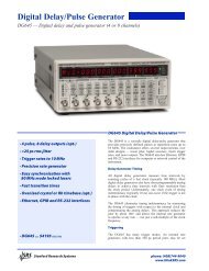
User Manual<strong>DG645</strong>Digital Delay GeneratorRevision 1.1 (9/9/08)
Certification<strong>Stanford</strong> <strong>Research</strong> <strong>Systems</strong> certifies that this product met its published specifications at the timeof shipment.WarrantyThis <strong>Stanford</strong> <strong>Research</strong> <strong>Systems</strong> product is warranted against defects in materials andworkmanship for a period of one (1) year from the date of shipment.ServiceFor warranty service or repair, this product must be returned to a <strong>Stanford</strong> <strong>Research</strong> <strong>Systems</strong>authorized service facility. Contact <strong>Stanford</strong> <strong>Research</strong> <strong>Systems</strong> or an authorized representativebefore returning this product for repair.Information in this document is subject to change without notice.Copyright © <strong>Stanford</strong> <strong>Research</strong> <strong>Systems</strong>, Inc., 2008. All rights reserved.<strong>Stanford</strong> <strong>Research</strong> <strong>Systems</strong>, Inc.1290-C Reamwood AvenueSunnyvale, California 94089Phone: (408) 744-9040Fax: (408) 744-9049www.thinkSRS.comPrinted in the U.S.A.<strong>DG645</strong> Digital Delay Generator
Contents iContentsContentsSafety and Preparation for UseSpecificationsQuick Start InstructionsivviixiIntroduction 1<strong>DG645</strong> Features and Performance 1Timebase Options 2Rear-Panel Options 4Front-Panel Accessory 6Front-Panel Overview 7Front-Panel BNCs 7Triggering 8Display 9Modify 9Status Indicators 12Rear-Panel Overview 13AC Power 13GPIB 13RS-232 14Ethernet 14Chassis Ground 14Timebase 14Inhibit 15Optional Rear-Panel Outputs 15Operation 17Front-Panel User Interface 17Power On 17<strong>DG645</strong> Main Display 18Store and Recall Settings 19Secondary Functions 20Triggering 20Internal Triggering 22External Triggering 22Single Shot Triggering 23Line Triggering 23Advanced Triggering 23Trigger Holdoff 24Trigger Prescaling 24Trigger Status 25Burst Mode 26<strong>DG645</strong> Digital Delay Generator
Contents iiDelays 27Linked Delays 27Levels 28Secondary Functions 29TTL 29NIM 29Positive OUT 29Negative OUT 29NET 29GPIB 31RS232 32DATA 32STATUS 33AB→ALL 34DISPL OFF 34LOCAL 35INIT 35CAL 35INHIBIT 36Factory Default Settings 36Troubleshooting 38<strong>DG645</strong> Remote Programming 41Introduction 41Interface Configuration 41GPIB 42RS-232 42LAN 43Front Panel Indicators 44Command Syntax 44Index of Commands 46Common IEEE-488.2 Commands 46Status and Display Commands 46Trigger Commands 46Burst Commands 47Delay and Output Commands 47Interface Commands 47Command List 48Common IEEE-488.2 Commands 48Status and Display Commands 50Trigger Commands 52Burst Commands 54Delay and Output Commands 56Interface Commands 57Status Byte Definitions 60<strong>DG645</strong> Digital Delay Generator
Contents iiiSerial Poll Status Byte 60Standard Event Status Register 61Instrument Status Register 61Error Codes 62DG535 Compatibility 68Example Programming Code 69<strong>DG645</strong> Calibration 73Calibration Bytes 73Automatic Delay Calibration 73Timebase Calibration 73Output Level Calibration 74Trigger Threshold Calibration 76Circuit Description 79Overview 79Block Diagram and IO 81External and PCB Interfaces 81Display PCB – J4 82Main Pulse Output PCB – J6 82Power Supply – J11 83Optional Oscillator Connector – J7 84Optional Rear-Panel Pulse Output – J8 85Ethernet – J10 85RS-232 – J2 85GPIB – J3 8510 MHz Reference Input – J9 8610 MHz Reference Output – J5 86Trigger Inhibit – J1 86Analog µP Interface 86Microcontroller 87Interface 88Subcircuits 90FPGA 91Interface 91FPGA Internal Subcircuits 93100 MHz Timebase 96Interface 96Subcircuits 97DDS & Trigger 99Interface 99Subcircuits 100Single Cycle and Line Trigger 101Time to Amplitude Convertor 101<strong>DG645</strong> Digital Delay Generator
Contents ivInterface 102Subcircuits 103Verniers 106Interface 107Subcircuits 108T0 & T1 Logic 109Interface 109Subcircuits 109A - D (E - H) Logic 110Interface 110Subcircuits 111GPIB 112Power Supply IO 112Front-Panel Display 112Power Supply 113Trigger Input and Front-Panel Outputs 114Ext Trig Input 114Front-Panel Output Drivers 114Rear-Panel Outputs 116Option 1: 8-Channel, 5V 116Option 2: 8-Channel, High Voltage 117Option 3: Combinatorial Logic Outputs 119Parts List 121Motherboard Assembly 121Output Driver Assembly 136Power Supply Assembly 143Front-Panel Display Assembly 145Chassis Assembly 147Option 1 Assembly 148Option 2 Assembly 150Option 3 Assembly 154Option 4 Assembly 156Option 5 Assembly 157Schematics 159<strong>DG645</strong> Schematic Diagram List 159<strong>DG645</strong> Digital Delay Generator
Safety and Preparation for Use vSafety and Preparation for UseLine VoltageThe <strong>DG645</strong> operates from a 90 to 132 VAC or 175 to 264 VAC power source having aline frequency between 47 and 63 Hz. Power consumption is less than 100 VA total. Instandby mode, power is turned off to the main board. However, power is maintained at alltimes to any optional timebases installed. Thus, a unit with an optional rubidium orovenized quartz oscillator is expected to consume less than 25 VA and 15 VA of power,respectively, in standby mode.Power Entry ModuleA power entry module, labeled AC POWER on the back panel of the <strong>DG645</strong>, providesconnection to the power source and to a protective ground.Power CordThe <strong>DG645</strong> package includes a detachable, three-wire power cord for connection to thepower source and protective ground.The exposed metal parts of the box are connected to the power ground to protect againstelectrical shock. Always use an outlet which has a properly connected protective ground.Consult with an electrician if necessary.GroundingA chassis grounding lug is available on the back panel of the <strong>DG645</strong>. Connect a heavyduty ground wire, #12AWG or larger, from the chassis ground lug directly to a facilityearth ground to provide additional protection against electrical shock.BNC shields are connected to the chassis ground and the AC power source ground via thepower cord. Do not apply any voltage to the shield.Line FuseThe line fuse is internal to the instrument and may not be serviced by the user.Operate Only with Covers in PlaceTo avoid personal injury, do not remove the product covers or panels. Do not operate theproduct without all covers and panels in place.Serviceable PartsThe <strong>DG645</strong> does not include any user serviceable parts inside. Refer service to aqualified technician.<strong>DG645</strong> Digital Delay Generator
Safety and Preparation for Use viSymbols you may Find on SRS ProductsSymbolDescriptionAlternating currentCaution - risk of electric shockFrame or chassis terminalCaution - refer to accompanying documentsEarth (ground) terminalBatteryFuseOn (supply)Off (supply)<strong>DG645</strong> Digital Delay Generator
Specifications viiSpecificationsDelaysChannels4 independent pulses controlled in position and width. 8 delaychannels available as an option (see Output Options).Range0 to 2000 sResolution5 psAccuracy1 ns + (timebase error × delay)Jitter (rms)Ext. trig to any output Delay 100 µs100MHz/N trigger rate
Specifications viiiBurst GeneratorTrigger to first T 0Range0 to 2000 sResolution5 psPeriod between pulsesRange100 ns to 42.9 sResolution10 nsDelay cycles per burst 1 to 2 32 − 1Outputs (T 0 , AB, CD, EF, and GH)Source impedance 50 ΩTransition time
Specifications ixOption 2 (8 High Voltage Delay Outputs on Rear Panel)Outputs (BNC)Source impedanceTransition timeLevelsPulse characteristicsRising edgeFalling edgeT 0 , A, B, C, D, E, F, G and H50 Ω
Quick Start Instructions xiQuick Start InstructionsStep by Step Example1. With the power button in the Standby position, connect the <strong>DG645</strong> to a groundedoutlet using the power cord provided.2. Press the power button “in” to turn on the unit.3. Press the following keys sequentially to load default settings: ‘RCL’, ‘0’,‘ENTER’.4. Press the TRIGGER ▲ key five times until the INT LED in the trigger section ofthe front panel is highlighted. This selects internal triggering.5. Trigger an oscilloscope on the rising edge of T0’s output, and display AB’soutput on the 1 µs/div scale.6. Press the ‘DELAY’ key to view the delay for channel A.7. Press the CURSOR ◄ and ► keys to the change the step size for channel A.8. Press the MODIFY ▲ and ▼ keys to modify the delay for channel A by thecurrent step size.9. Press ‘1’, ‘µs’ to set the delay for channel A to 1 µs. (Note that the ‘µs’ key isshared with the MODIFY ▼ key.) The oscilloscope should show the AB outputmove one division after the trigger.10. Press the EDGE ◄ and ► keys to select different delays.11. Refer to the detailed instructions that follow for more information on theoperation of the <strong>DG645</strong>.<strong>DG645</strong> Digital Delay Generator
Introduction 1Introduction<strong>DG645</strong> Features and PerformanceThe <strong>DG645</strong> Digital Delay Generator is a precision 8-channel delay generator that canoutput arbitrary delays from 0 to 2000 s with 5 ps resolution and typical rms jitterof 12 ps.The <strong>DG645</strong> provides front-panel BNC connectors for five delay outputs: T0, AB,CD, EF, and GH. Internally, the <strong>DG645</strong> generates 8 user-defined time events: A,B, C, D, E, F, G, and H. The timing events have a range of 2000 s and precisionof 5 ps. The front-panel outputs pair these timing events to produce four outputpulses: AB, CD, EF, and GH. In addition, a T0 output is asserted at t=0 andremains asserted until the longer of the trigger holdoff or 25 ns after the longestdelay. Outputs may be configured with offsets ranging over ±2 V and amplitude stepsfrom 0.5 to 5.0 V with positive or negative polarity. Both rising and falling edges are
Introduction 2A burst generator enables the user to generate a burst of delay cycles with a singletrigger. The trigger source can be internal or external. The user can configure the delayfrom the trigger to the first burst delay cycle, the period between delay cycles, and thenumber of delay cycles per burst.A 10 MHz input enables the <strong>DG645</strong> to synchronize its internal clock to an externalreference. A 10 MHz output is provided to synchronize external instrumentation tothe <strong>DG645</strong>.The <strong>DG645</strong> naturally supports remote control via a host computer. The <strong>DG645</strong> comesstandard with support for GPIB (IEEE 488.2), RS-232, and LAN TCP/IP connections. Ahost computer interfaced to the <strong>DG645</strong> can perform virtually any operation that isaccessible from the front panel.Timebase OptionsThe <strong>DG645</strong>’s standard timebase has an rms jitter of
Introduction 31 ms100 µsOCXO Timebase(opt. 4)Standard TimebaseMax. Error (after 1 yr.)10 µs1 µs100 ns10 nsRubidium Timebase(opt. 05)Ideal External Timebase1 ns100 ps10 µs 100 µs 1 ms 10 ms 100 ms 1 s 10 s 100 s 1000 sDelayJitter (rms)10 µs1 µs100 ns10 ns1 nsFigure 2: Typical <strong>DG645</strong> Timing Error 1 Year after CalibrationRubidium Timebase(opt. 05)Ideal External TimebaseOCXO Timebase(opt. 4)Standard Timebase100 ps10 ps10 µs 100 µs 1 ms 10 ms 100 ms 1 s 10 s 100 s 1000 sDelayFigure 3: Typical rms Jitter vs. Delay Setting<strong>DG645</strong> Digital Delay Generator
Introduction 4Rear-Panel OptionsInternally, the <strong>DG645</strong> generates 8 user-defined time events: A, B, C, D, E, F, G, and H.The timing events have a range of 2000 s with 5 ps resolution. The front-panel outputspair these timing events to produce four output pulses: AB, CD, EF, and GH. In addition,a T0 output is asserted at t=0 and remains asserted until the longer of the trigger holdoffor 25 ns after the longest delay. One of three rear-panel output modules may optionallybe installed to provide the user with 9 additional delay outputs in various combinations.Option 1: 8-Channel OutputsRear-panel Option 1 provides access to each of the 8 timing events, independently, byproducing an output at T0 and at each of the 8 user-defined time events: A, B, C, D, E, F,G, and H. All of these outputs use positive 5 V logic (2.5 V into 50 Ω), going high attheir programmed delay and going low after the longer of the trigger holdoff or 25 nsafter the longest programmed delay. There is no duty cycle limitation for these outputs.Figure 4 summarizes these outputs.ToABCDEFGH5 V0 VABCDEFG25 nsHFigure 4: Option 1 Rear-Panel Outputs vs. Programmed Delay<strong>DG645</strong> Digital Delay Generator
Introduction 5Option 2: 8-Channel High Voltage OutputsRear-panel Option 2 provides 8 timing events independently by producing an output atT0 and at each of the 8 user-defined time events: A, B, C, D, E, F, G, and H. All of theseoutputs use positive 30 V logic (15 V into 50 Ω), going high at their programmed delayfor a period of about 100 ns.ToABCD30 V0 V100 nsABCDEEFFGGHHFigure 5: Option 2 Rear Panel Outputs vs Programmed DelayEach of the nine outputs can drive a 50 Ω load to +15 V, requiring a total current of9×15/50 = 2.7 A. The peak power of 108 W cannot be maintained, and so the outputamplitude is reduced as the duty cycle is increased. As is detailed in Figure 6, the outputpulse amplitude is reduced by less than 1 % per kHz of trigger rate.Option 2 Pulse Amplitude vs Trigger RatePercent of Full Amplitude1008060402001 10 100 1000Trigger Rate in kHzFigure 6: Option 2 Amplitude Reduction vs. Trigger Rate<strong>DG645</strong> Digital Delay Generator
Introduction 6Option 3: Combinatorial Logic OutputsRear-panel Option 3 provides copies of the front panel outputs on the rear panel. Inaddition, the logical OR of AB + CD, EF + GH, AB + CD + EF andAB + CD + EF + GH are also provided to give 1, 2, 3, or 4 precisely defined pulses onseparate BNC outputs. All of these outputs use positive 5 V logic (2.5 V into 50 Ω),going high for the time between their programmed delays. There is no duty cyclelimitation for these outputs.5 V0 VToABCDAB+CDEFGHEF+GHAB+CD+EFAB+CD+EF+GHABCDEFGHFigure 7: Option 3 Rear-Panel Outputs vs. Programmed DelayFront Panel AccessorySRD 1: Fast Rise Time ModuleThe SRD 1 is a front-panel accessory that can generate fast rise times of
Introduction 7Front-Panel OverviewThe front panel was designed to provide a simple, intuitive user interface to all the<strong>DG645</strong> features (see Figure 8). The power switch is located in the lower right corner ofthe front panel. Pushing the switch enables power to the instrument. Pushing the switchagain places the instrument in stand-by mode, where power is enabled only to optionallyinstalled timebases. Power to the main board is turned off in stand-by mode.The front panel is divided into four sections to indicate overall functionality: TRIGGER,DISPLAY, MODIFY, and STATUS. Keys in the TRIGGER section allow the user toselect the type of triggering desired. Keys in the DISPLAY section control what is shownin the main display. Keys in the MODIFY section are used for changing the currentlydisplayed item to a specific value or incrementing it by configurable steps. This section isalso used to access secondary functions. LEDs in the STATUS section indicate the statusof external timebases and remote interfaces.The front panel also includes five BNC connectors which provide an external triggerinput and five delay outputs for connecting the <strong>DG645</strong> delay signals to user applicationsvia standard BNC cables.Front-Panel BNCsExternal Trigger InputFigure 8: The <strong>DG645</strong> Front PanelThis BNC is labeled EXT TRIG, and it is located in the lower left corner of the frontpanel. If external triggering is selected, this input provides an external signal fortriggering the five delay outputs. It has a 1 MΩ input resistance and can be configured forrising or falling edge triggers with thresholds that can range over ±3.5 V.<strong>DG645</strong> Digital Delay Generator
Introduction 8Delay Signal OutputsThere are five delay channel outputs on the front panel. They are labeled T0, AB, CD,EF, and GH. All the outputs have 50 Ω source impedances and should be terminated into50 Ω loads. The amplitude, offset, and polarity of each output is programmable from thefront panel. Amplitudes can range from 0.5 V to 5.0 V. Offsets can range over ±2.0 V.Polarities can be positive or negative. Channel T0 is always programmed to output apulse that starts at a time defined as T ≡ 0 s and ends after the longer of the triggerholdoff or 25 ns after all other programmed delays have completed. The rest of thechannels, AB through GH, have user programmable delay outputs. Channel AB has twoprogrammable delays associated with it: delay A and delay B. Delay A is typically thestarting edge and delay B, the trailing edge. Together, these two delays enable the user tocontrol both the delay and the pulse width of the output relative to the T0 output.Channels CD, EF and GH behave similarly.TriggeringThe TRIGGER section of the front-panel display controls the triggering of the <strong>DG645</strong>.The ▲ and ▼ keys in this section select one of seven different triggering modes listed inTable 2.Table 2: <strong>DG645</strong> Triggering ModesLabelDescriptionINTInternal triggering at rates from 100 µHz to 10 MHz.EXT External triggering on rising edgesEXT External triggering on falling edgesSNGL EXT Externally triggered single shot on a rising edge*SNGL EXT Externally triggered single shot on a falling edges*SNGLSingle shot triggeringLINETrigger at the power line frequency* Note that externally triggered single shots are denoted when both SNGL and thegiven EXT LEDs are lit.LEDs in the TRIGGER section indicate which triggering mode is currently active as wellas the triggered status of the <strong>DG645</strong>. The trigger rate and external trigger threshold maybe displayed and modified by pressing the ‘TRIG’ key in the display section. Single shottriggering can be initiated from the front panel by pressing the ‘ENTER’ key when themain display reads ‘TRG SINGLE SHOT.’The <strong>DG645</strong> can be synchronized with trigger sources operating at up to 100 MHz byprogramming a trigger hold off time or enabling the trigger input prescaler. For detailedinformation about configuring these options, see Trigger Holdoff (page 24) or TriggerPrescaling (page 24).<strong>DG645</strong> Digital Delay Generator
Introduction 11LabelTTLNIMOUTOUTNETGPIBRS232DATASTATUSAB→ALLDISP OFFLOCALINITCALINHIBITTable 5: Secondary FunctionsFunction DescriptionSet the selected output to TTL levels: 0 to 4 VSet the selected output to NIM levels: -0.8 to 0 VConfigure selected output with positive polarityConfigure selected output with negative polarityConfigure TCPIP interfaceConfigure GPIB interfaceConfigure RS232 interfaceDisplay the most recent data received over any remote interfaceView TCPIP, error, or instrument statusCopy channel AB settings to all other channelsTurn off the front-panel displayGo to local. Enables front-panel keys if in remote mode.Load default instrument settingsAuto cal the front-panel delays for optimum jitter performance.Configure the rear-panel INHIBIT input.A more detailed description of each of the secondary functions is given in the SecondaryFunctions section of the Operation chapter (page 29).The secondary functions can only be accessed when SHIFT mode is active, which isindicated by the SHIFT LED being turned on. The SHIFT mode can be toggled on andoff by pressing the ‘SHIFT’ key. Therefore, to configure the current channel to outputTTL levels, you would press the ‘SHIFT’ key to activate SHIFT mode, and then press‘BACK SPACE’ to execute the TTL secondary function.Most of the secondary functions will automatically toggle SHIFT mode off whenexecuted. NET, GPIB, RS232, and STATUS are exceptions to this rule because theyhave multiple menu options to display. Use the MODIFY ▲ and ▼ keys to modify aparameter. Press the secondary function key repeatedly to move between menu options.For example, pressing ‘SHIFT’, ‘STO’ sequentially causes the TCPIP configurationmenu to be displayed. The first option is TCPIP ENABLE/DISABLE. Use the MODIFY▲ and ▼ keys to change the setting as desired. Then press ‘STO’ again to move to thenext option which is DHCP ENABLE/DISABLE. Continue pressing ‘STO’ until allTCPIP settings have been configured as desired.Secondary functions that have an arrow ( ) printed after them, such as AB→ALL, INIT,CAL, and INHIBIT, require that the user press the ‘ENTER’ key to complete the action.For example, to initialize the instrument to its default settings, you would sequentiallypress ‘SHIFT’, ‘INIT’, ‘ENTER’.CancelThe ‘SHIFT’ key also functions as a general purpose CANCEL key. Any numeric entry,which has not been completed by pressing a units key, can be canceled by pressing the‘SHIFT’ key. Because of the dual role played by the SHIFT key, the user may have topress ‘SHIFT’ twice to reactivate SHIFT mode. The first key press cancels the currentaction, and the second key press activates SHIFT mode.<strong>DG645</strong> Digital Delay Generator
Introduction 12Status IndicatorsTIMEBASEIn the upper right portion of the front panel are two groups of LED indicators. The uppergroup is labeled TIMEBASE. This contains the EXT and ERR LEDs. The EXT LEDindicates that the <strong>DG645</strong> has detected an external 10 MHz reference at the 10 MHz inputBNC on the rear panel of the <strong>DG645</strong>. The <strong>DG645</strong> will lock its internal clock to thisexternal reference.The ERR LED indicates that <strong>DG645</strong> has not yet locked its internal timebase to anexternal input 10 MHz timebase. Normally, this LED will only flash momentarily whenan external timebase is first applied to the rear input. If the LED stays on, it indicates thatthe <strong>DG645</strong> may be unable to lock to the external timebase. This is most commonlycaused by an input frequency which is offset from 10 MHz by more than 10 ppm.INTERFACEThe lower group of LED indicators is labeled INTERFACE. These LEDs indicate thecurrent status of the TCP/IP, RS-232, or GPIB remote programming interfaces. The REMLED turns on when the <strong>DG645</strong> is placed in remote mode by one of the remote interfaces.In this mode, all the front-panel keys are disabled and the instrument can only becontrolled via the remote interface. The user can return to normal, local mode by pressingthe ‘3’ key once. The ‘LOCAL’ label above the key indicates the dual functionality ofthis key. The ACT LED flashes when a character is received or sent over one of theinterfaces. This is helpful when troubleshooting communication problems. If a commandreceived over the remote interface fails to execute due to either a parsing error or anexecution error, the ERR LED will turn on and stay on until the status display isaccessed. Information about the error is available in the STATUS secondary display.<strong>DG645</strong> Digital Delay Generator
Introduction 13Rear-Panel OverviewThe rear panel provides connectors for AC power, GPIB/RS-232/TCPIP computerinterfaces, chassis ground, external timing references, inhibit input, and various optionaladditional delay outputs (see Figure 9).AC PowerGPIBFigure 9: The <strong>DG645</strong> Rear PanelThe Power Entry Module is used to connect the <strong>DG645</strong> to a power source through thepower cord provided with the instrument. The center pin is connected to the <strong>DG645</strong>chassis so that the entire box is grounded.The source voltage requirements are 90 to 132 VAC or 175 to 264 VAC, 47 to 63 Hz(100 VA total).Connect the <strong>DG645</strong> to a properly grounded outlet. Consult an electrician if necessary.The <strong>DG645</strong> comes standard with a GPIB (IEEE-488) communications port forcommunications over a GPIB bus. The <strong>DG645</strong> supports the IEEE-488.1 (1978) interfacestandard. It also supports the required common commands of the IEEE-488.2 (1987)standard.Before attempting to communicate with the <strong>DG645</strong> over the GPIB interface, the GPIBaddress must configured by pressing the keys ‘SHIFT’, ‘GPIB’, ‘GPIB’. Use theMODIFY ▲ and ▼ keys to select the desired address. Then, either power-cycle the unitor reset the interface to ensure that the new interface settings are active.<strong>DG645</strong> Digital Delay Generator
Introduction 14RS-232EthernetA host computer interfaced to the <strong>DG645</strong> can perform virtually any operation that isaccessible from the front panel. Programming the <strong>DG645</strong> is discussed in the <strong>DG645</strong>Remote Programming chapter.The <strong>DG645</strong> comes standard with an RS-232 communications port. The RS-232 interfaceconnector is a standard 9 pin, type D, female connector configured as a DCE (transmit onpin 3, receive on pin 2). The baud rate is configurable from the front panel, but the rest ofthe communication parameters are fixed at 8 data bits, 1 stop bit, no parity, RTS/CTShardware flow control.Before attempting to communicate with the <strong>DG645</strong> over RS-232, the baud rate must beconfigured by pressing the following keys: ‘SHIFT’, ‘RS232’, ‘RS232’. Use theMODIFY ▲ and ▼ keys to select the desired baud rate. Then, either power-cycle theunit or reset the interface to ensure that the new interface settings are active.A host computer interfaced to the <strong>DG645</strong> can perform virtually any operation that isaccessible from the front panel. Programming the <strong>DG645</strong> is discussed in the <strong>DG645</strong>Remote Programming chapter.The <strong>DG645</strong> comes standard with an RJ-45 connector for connecting it to an Ethernetbased local area network (LAN) using standard Category-5 or Category-6 cable. Itsupports 100 Base-T Ethernet connections.Before attempting to communicate with the <strong>DG645</strong> over a LAN, the IP address, subnetmask address, and the default router must be configured. The <strong>DG645</strong> supports automaticconfiguration of these parameters via DHCP or AUTO-IP. Manual configuration of astatic IP address is also supported. Refer to the LAN Configuration section of the <strong>DG645</strong>Remote Programming chapter for details on configuring the TCPIP interface.A host computer interfaced to the <strong>DG645</strong> can perform virtually any operation that isaccessible from the front panel. Programming the <strong>DG645</strong> is discussed in the <strong>DG645</strong>Remote Programming chapter.Chassis GroundUse this grounding lug to connect the <strong>DG645</strong> chassis directly to facility ground.Timebase10 MHz INThe <strong>DG645</strong> provides a 10 MHz BNC input for synchronizing its internal clock to anexternal 10 MHz reference. The external reference should provide greater than 0.5 V ppinto a 1 kΩ impedance. The <strong>DG645</strong> will automatically detect the presence of an external10 MHz reference and lock to it if possible. If the <strong>DG645</strong> is unable to lock to the externalreference, the front-panel TIMEBASE ERR LED will turn on and stay on until the<strong>DG645</strong> either successfully locks to the external reference or the reference is removed.<strong>DG645</strong> Digital Delay Generator
Introduction 15Inhibit10 MHz OUTThe <strong>DG645</strong> provides a 10 MHz BNC output for synchronizing other instrumentation tothe <strong>DG645</strong>’s timebase.The <strong>DG645</strong> provides an inhibit BNC input for inhibiting triggers or various delayoutputs. When the inhibit input is logic high (>2.0 V) either the trigger or the configuredoutput is inhibited for that delay cycle. See the Inhibit section of the Operation chapter(page 36) for more information about configuring the inhibit functionality.Optional Rear-Panel OutputsThe <strong>DG645</strong> may be extended with 9 additional delay outputs on the rear panel. Threedifferent combinations of outputs are available: 8-Channel CMOS logic outputs,8-Channel HV outputs, or 4-Channel CMOS combinatorial logic outputs. For moreinformation about these optional outputs, see Rear-Panel Options on page 4.<strong>DG645</strong> Digital Delay Generator
Operation 17OperationFront-Panel User InterfaceThe previous chapter described the function of the front-panel keys based on theirlocation on the front panel. This section provides guidelines for viewing and changinginstrument parameters independent of their location on the front panel.Power OnAt power on, the <strong>DG645</strong> will briefly display “<strong>DG645</strong>” followed by the firmware versionand the unit serial number. When power on initialization has completed, the <strong>DG645</strong> willrecall the latest known instrument settings from nonvolatile memory and be ready for use.The <strong>DG645</strong> continuously monitors front-panel key presses and will save the currentinstrument settings to nonvolatile memory after approximately five seconds of inactivity.To prevent the nonvolatile memory from wearing out, however, the <strong>DG645</strong> will notautomatically save instrument settings that change due to commands executed over theremote interface. The remote commands *SAV and *RCL can be used to explicitly saveinstrument settings over the remote interface, if desired. See the <strong>DG645</strong> RemoteProgramming chapter for more information about these commands.The <strong>DG645</strong> can be forced to boot up at factory default settings. This is accomplished bypressing and holding the ‘BACK SPACE’ key during power up, until the initialization iscomplete. All instrument settings, except for the remote interface configurations, will beset back to their default values. All calibration bytes will be reset to the values set at thefactory at the time of shipment. See the Factory Default Settings section on page 36 for alist of default settings.The remote interface configurations can also be forced back to their factory defaultsettings by pressing and holding the ‘STO’ key during power up initialization.<strong>DG645</strong> Digital Delay Generator
Operation 18<strong>DG645</strong> Main DisplayDisplay MenusThe <strong>DG645</strong> has four main display menus which are activated by dedicated keys in theDISPLAY section of the front panel. The function of each key is summarized in Table 6.LabelTRIGBURSTDELAYLEVELTable 6: DISPLAY Section KeysValue Shown in Main Display When PressedTrigger rate, trigger threshold, trigger holdoff, ortrigger prescaler configurationBurst configurationChannel delay settingsFront-panel output configuration including offset,amplitude and polarity.Display NavigationEach display menu contains one or more instrument settings which may be successivelyviewed by pressing the given display key multiple times. For example, the LEVEL menuhas three parameters that may be changed: offset, amplitude (step), and polarity. When‘LEVEL’ is pressed the first time, output offset is displayed. Pressing ‘LEVEL’ a secondtime causes the output amplitude to be displayed. Pressing ‘LEVEL’ a third time causesoutput polarity to be displayed. Pressing ‘LEVEL’ yet again causes the output offset to bedisplayed again.Edge KeysThe DELAY and LEVEL menus are tied to one of the five front-panel outputs labeledT0, AB, CD, EF, and GH. LEDs above the outputs indicate the currently selected output.The EDGE ◄ and ► keys enable the user to navigate among the leading and trailingedges of the various outputs. For example, if the delay menu is active and the LED on theleft side of the AB output is lit, then the channel A delay will be shown in the maindisplay. Pressing EDGE ► once will cause the LED on the right side of the AB output tolight and the channel B delay to be displayed. Pressing EDGE ► again will cause thechannel C LED and delay to display.Cursor KeysMost instrument settings have an independent step size associated with it. This isindicated by a blinking digit called the cursor. The cursor indicates which digit will bechanged when the MODIFY ▲ and ▼ keys are pressed. The CURSOR ◄ and ► keys inthe DISPLAY section enable the user to move the cursor left and right respectively. Eachpress of a CURSOR key increases or decreases the associated step size for the displayedparameter by a factor of 10.Step SizesAlthough the CURSOR keys enable the user to quickly change the step size by exactfactors of 10, sometimes it is desirable to set an arbitrary step size. Located below the<strong>DG645</strong> Digital Delay Generator
Operation 19MODIFY ▲ and ▼ keys is the ‘STEP SIZE’ key. Pressing ‘STEP SIZE’ enables theuser to view and modify the current step size associated with a parameter. When the stepsize for a parameter is displayed, the STEP LED in the main display will be highlighted.Once displayed, the step size may be increased or decreased by exact factors of 10 bypressing the MODIFY ▲ and ▼ keys. Alternatively, an arbitrary step size may beentered with the numeric keys and completing the entry by pressing an appropriate unitskey. (Note that the units keys are shared with the MODIFY ▲, ▼, ‘STEP SIZE’ and‘ENTER’ keys.)For example, if the channel A delay is currently displayed and the 1 ns digit is blinking,then the current step size for channel A is 1 ns. Pressing ‘STEP SIZE’ once will cause thedisplay to show ‘STP 000.000000001000’. Pressing the keys ‘2’, ‘5’, ‘ns’ sequentially,will change the current step size to 25 ns. Pressing ‘STEP SIZE’ again will cause channelA delay to display again, except that now the current step size is 25 ns and so the 10 nsdigit will be blinking to indicate that the 10 ns digit will change when the delay isstepped. Continuing with the example, if the current delay for channel A is 0 ns, thenpressing MODIFY ▲ will step up the delay to 25 ns.Changing a ParameterTo change a parameter, enter a new value using the numeric keys in the MODIFY sectionof the front panel, and complete the entry by pressing an appropriate units key. (Note thatthe units keys are shared with the MODIFY ▲, ▼, ‘STEP SIZE’ and ‘ENTER’ keys.)Generally speaking, only the parameter shown in the main display can be changed. Forexample, to change the delay for channel A, press the ‘DELAY’ key to show delays.Then use EDGE ◄ and ► keys to navigate the display to channel A. To set the delay to10 µs press the following keys sequentially: ‘1’, ‘0’ ‘µs’. Pressing ‘1’ initiates theparameter change, while pressing ‘µs’ completes entry and sets the delay to 10 µs.If the user enters extra digits beyond the allowed resolution of a parameter, the extradigits will be rounded to the nearest allowed digit. For example, entering a voltage offsetof 2.005 V will result in the offset being rounded to 2.01 V. (Outputs have a voltageresolution of 10 mV.)Stepping a ParameterMost parameters can be stepped up and down by their associated step sizes byrespectively pressing the ▲ and ▼ keys in the MODIFY section of the front panel. Forexample, if channel A delay is currently being displayed as ‘A=0+000.001234567890’and 4 is blinking, then the current step size is 1 µs. Pressing MODIFY ▲ will change thedelay to ‘A=0+000.001235567890’. Pressing MODIFY ▼ will bring the delay back to‘A=0+000.001234567890’.Store and Recall SettingsThe ‘STO’ and ‘RCL’ keys are for storing and recalling instrument settings. Theinstrument saves the trigger mode, burst configuration, all delays, all levels, all associatedstep sizes, and the current display. Up to nine different instrument settings may be storedin the locations 1 to 9. To save the current settings to location 5, for example, press thekeys ‘STO’, ‘5’, ‘ENTER’. To recall instrument settings from location 5, press the keys‘RCL’, ‘5’, ‘ENTER’. The user may also use the MODIFY ▲ and ▼ keys to select the<strong>DG645</strong> Digital Delay Generator
Operation 20desired location, rather than enter the location directly with the numeric keys. The<strong>DG645</strong> will remember the last location used for store and recall. To reuse theremembered location, simply skip the numeric entry when storing or recalling settings.For example, to recall settings from the remembered location, the user should simplypress ‘RCL’, ’ENTER.’ Location 0 is reserved for recalling default instrument settings.See Factory Default Settings on page 36 for a list of default settings.Secondary FunctionsTriggeringMost of the keys in the MODIFY section of the front panel have secondary functionsassociated with them. The names of these functions are printed above the key. The ‘4’key, for example, has RS232 above it.The secondary functions can only be accessed when SHIFT mode is active, which isindicated by the SHIFT LED being turned on. The SHIFT mode can be toggled on andoff by pressing the ‘SHIFT’ key. Therefore, to configure the currently highlighted outputBNC with positive polarity, you would press the ‘SHIFT’ key to activate SHIFT mode,and then press ‘8’ to execute OUT.Most of the secondary functions will automatically toggle SHIFT mode off whenexecuted. NET, GPIB, RS232 and STATUS are exceptions to this rule because they havemultiple menu options to display. Use the MODIFY ▲ and ▼ keys to modify aparameter. Press the secondary function key repeatedly to move between menu options.For example, pressing ‘SHIFT’, ‘STO’ sequentially causes the TCPIP configurationmenu to be displayed. The first option is TCPIP ENABLE/DISABLE. Use the MODIFY▲ and ▼ keys to change the setting as desired. Then press ‘STO’ again to move to thenext option, which is DHCP ENABLE/DISABLE. Continue pressing ‘STO’ until allTCP/IP settings have been configured as desired.Secondary functions that have an arrow ( ) printed after them, such as AB→ALL, INIT,CAL, and INHIBIT, require that the user press the key ‘ENTER’ to complete the action.For example, to initialize the instrument to its default settings, you would sequentiallypress ‘SHIFT’, ‘INIT’, ‘ENTER.’Detailed descriptions of each of the secondary functions can be found later in thischapter.The <strong>DG645</strong> supports seven different triggering modes listed in Table 7. The ▲ and ▼keys in TRIGGER section of the front-panel display enable the user to select the desiredtriggering mode. LEDs in the TRIGGER section indicate which triggering mode iscurrently active as well as the trigger status of the <strong>DG645</strong>.<strong>DG645</strong> Digital Delay Generator
Operation 21Table 7: <strong>DG645</strong> Triggering ModesLabelDescriptionINTInternal triggering at rates from 100 µHz to 10 MHz.EXT External triggering on rising edgesEXT External triggering on falling edgesSNGL EXT Externally triggered single shot on a rising edge*SNGL EXT Externally triggered single shot on a falling edges*SNGLSingle shot triggeringLINETrigger at the power line frequency* Note that externally triggered single shots are denoted when both SNGL and thegiven EXT LEDs are lit.To access the trigger configuration from the front panel, press the ‘TRIG’ key in theDISPLAY section of the front panel. The trigger menu options are summarized inTable 8. Press the ‘TRIG’ key to cycle between menu options. Use the MODIFY ▲ and▼ keys or the numeric keypad to modify parameters.Table 8: <strong>DG645</strong> Trigger MenuLED Label Example Display DescriptionTRIG RATE ‘TRG 1000.000000’ Internal trigger rateTRIG THRES ‘TRG THRES 1.00’ External trigger inputthresholdSTATUS ‘ADV. TRIGGERING ON’ Enable/disable advancedtriggeringSTATUS ‘HOLD 0.000010000000’ Trigger holdoff timeSTATUS ‘TRG PRESCALE 100’ Prescaler configurationparameterNote that the trigger holdoff and prescaler configurations menu items will only beaccessible if advanced triggering is enabled.The prescaler configuration parameters are tied to a given front-panel output. Use theEDGE ◄ and ► keys to select the various parameters. The prescaler configurationparameters are summarized in Table 9.<strong>DG645</strong> Digital Delay Generator
Operation 22Table 9: <strong>DG645</strong> Prescaler ConfigurationEdge Example Display DescriptionT0 ‘TRG PRESCALE 1000’ Prescale triggers by the givencount. In this case, a delay cyclewill be generated once every 1000triggers.A,C,E,G ‘AB PRESCALE 10 Prescale the front-panel ABoutput by the given count. In thiscase, the AB output would beenabled once every 10successfully triggered delaycycles.B,D,F,H ‘AB PHASE 5’ Shift the phase of the AB outputenable to the given cycle. In thiscase, the 5 th delay cycle would beenabled. This would be followedby the 15 th , 25 th , etc.Internal TriggeringThe <strong>DG645</strong> has an internal rate generator that can generate triggers at rates from 100 µHzto 10 MHz with 1 µHz resolution. The generator uses DDS technology to generatetriggers with pulse-to-pulse rms jitter of
Operation 23To select external triggering press the TRIGGER ▲ and ▼ keys until EXT or EXTLED is highlighted for rising and falling edge triggers, respectively.Once external triggering is selected, the user can view and modify the trigger thresholdby pressing the ‘TRIG’ key in the DISPLAY section of the front panel. If the triggerthreshold is 1.0 V, then the main display will show ‘TRG THRES 1.00’, and the TRIGTHRES LED just below the main display will be highlighted. Once displayed, the usercan modify the trigger rate using any of the methods discussed in the section Front-PanelInterface earlier in this chapter.Single Shot TriggeringThe <strong>DG645</strong> supports single shot triggering. Single shot triggering enables the user totrigger the <strong>DG645</strong> one shot at a time.Normal Single ShotNormal single shot triggering is selected by pressing the TRIGGER ▲ and ▼ keys untilthe SNGL LED is highlighted by itself. To initiate a single shot, first press the ‘TRIG’key in the DISPLAY section once or twice until the display shows ‘TRG SINGLESHOT.’ Once this is displayed, the user initiates single shots by pressing the ‘ENTER’key.Externally Triggered Single ShotExternally triggered single shots are selected by pressing the TRIGGER ▲ and ▼ keysuntil the SNGL LED and either EXT or EXT LED is highlighted for rising andfalling edge triggers. To initiate a single shot, first press the ‘TRIG’ key in the DISPLAYsection successively until the display shows ‘TRG SINGLE SHOT.’ Once this isdisplayed, the user arms the <strong>DG645</strong> to accept a single external trigger by pressing the‘ENTER’ key. The display will show ‘TRG RDY SINGLE SHOT’ when the unit isarmed, but not yet triggered.Line TriggeringThe <strong>DG645</strong> can be triggered at the power line frequency by selecting line triggering. Thiswill typically be at either 50 or 60 Hz, depending on in which country the unit isoperated.To select line triggering, press the TRIGGER ▼ key until the LINE LED is highlighted.When line triggering is selected, pressing the ‘TRIG’ key in the DISPLAY section willcause the main display to show ‘TRG LINE’ and the TRIG RATE LED just below themain display to be highlighted.Advanced TriggeringThe <strong>DG645</strong> supports a number of complex triggering requirements via trigger holdoffand prescaling registers. These features are normally disabled, but they become enabledand accessible when advanced triggering is turned on. To enable advanced triggering,press ‘TRIG’ until the display shows ‘ADV. TRIGGERING OFF’, and then pressMODIFY ▲ to turn it on.<strong>DG645</strong> Digital Delay Generator
Operation 24Trigger HoldoffTrigger holdoff sets the minimum allowed time between successive triggers. Forexample, if the trigger holdoff is set to 10 µs, then successive triggers will be ignoreduntil at least 10 µs have passed since the last trigger. The red RATE LED will flash witheach ignored trigger. Specifying holdoff is useful if a trigger event in your applicationgenerates a significant noise transient that must have time to decay away before the nexttrigger is generated.Trigger holdoff can also be used to trigger the <strong>DG645</strong> at a sub-multiple of a known inputtrigger rate. For example, by selecting LINE as the trigger source and setting the holdoffto 0.99 s, the <strong>DG645</strong> can be triggered synchronously with the power line, but at 1 Hz.This technique works as long as the timebase of the trigger source doesn’t varysignificantly relative to the <strong>DG645</strong>’s timebase. Otherwise, trigger prescaling shouldbe used.Note that trigger holdoff is available only after advanced triggering is enabled. Onceadvanced triggering is enabled, the user can view and modify the trigger holdoff bysuccessively pressing the ‘TRIG’ key in the DISPLAY section of the front panel until thedisplay prefix is ‘HOLD’. If the trigger holdoff is 10 µs, then the main display will show‘HOLD 0.000010000000’, and the STATUS LED just below the main display will behighlighted. Once displayed, the user can modify the trigger holdoff using any of themethods discussed in the section Front-Panel Interface earlier in this chapter.Trigger PrescalingThe <strong>DG645</strong> supports a number of complex triggering requirements through a set of prescalingregisters. Trigger prescaling enables the <strong>DG645</strong> to be triggered synchronously with a much fastersource, but at a sub-multiple of the original trigger frequency. For example, the <strong>DG645</strong> can betriggered at 1 kHz, but synchronously with a mode locked laser running at 80 MHz, by prescalingthe trigger input by 80,000.Furthermore, the <strong>DG645</strong> also contains a separate prescaler for each front panel output thatenables it to operate at a sub-multiple of the prescaled trigger input frequency. Continuing withthe example above, if the AB prescaler is set to 100, the AB output will only be enabled for 1 outof every 100 delay cycles which is equivalent to a rate of 1 kHz/100 = 10 Hz.Lastly, the <strong>DG645</strong> contains a separate phase register for each output prescaler that determines thephase of the prescaler output relative to the other prescaled outputs. For example, if both the ABand CD prescalers are set to 100 and their phase registers to 0 and 50, respectively, then AB andCD will both run at 10 Hz, but CD’s output will be enabled 50 delay cycles after AB’s output.<strong>DG645</strong> Digital Delay Generator
Operation 25TriggerSourceF TrigTriggerPrescaler÷ NF T0Delay GeneratorOutputsTrigger T0F T0WhereF T0 = F Trig / NF AB = F T0 / M ABF CD = F T0 / M CDF EF = F T0 / M EFF GH = F T0 / M GHOutput Prescalers÷ M AB + θ AB÷ M CD + θ CD÷ M EF + θ EF÷ M GH + θ GHF ABF CDF EFF GHEnablesABCDEFGHABCDEFGHFigure 10: The <strong>DG645</strong> Trigger PrescalingThe <strong>DG645</strong>’s trigger prescaling operation is summarized in Figure 10. The trigger prescalervalue, N, can range from 1 to 2 30 − 1. The channel prescaler values, M, can range from 1 to2 16 − 1. Phase values may range from 0 to M – 1.Note that trigger prescaling is not available in single shot modes. In other modes, triggerprescaling is available only after advanced triggering is enabled. Once advanced triggering isenabled, the user can access the prescaler configuration by pressing the ‘TRIG’ until the displayshows ‘TRG PRESCALE 1’, and then pressing the EDGE ◄ and ► keys to select the desiredprescaler configuration parameter. The user can modify the various prescale factors using any ofthe methods discussed in the section Front-Panel Interface earlier in this chapter.Trigger StatusTrigger status of the <strong>DG645</strong> is indicated by the four LEDs shown in Table 10.LabelTRIG’DBURSTRATEINHTable 10: <strong>DG645</strong> Trigger StatusDescriptionTurns on when the <strong>DG645</strong> receives a valid trigger.Turns off when all delays are complete.Turns on when burst mode is active. Otherwise, off.Flashes when the <strong>DG645</strong> receives a trigger while adelay is still in progress. The trigger is ignored.Flashes when the <strong>DG645</strong> receives a trigger that wasinhibited via the rear-panel INHIBIT input or whileinstrument settings are being modified<strong>DG645</strong> Digital Delay Generator
Operation 26Burst ModeThe <strong>DG645</strong> has the ability to generate a burst of N delay cycles on each trigger. Thetrigger which generates the burst may come from any of the <strong>DG645</strong> trigger modes. Theuser can configure the number of delay cycles in the burst, the period between delaycycles, and the delay before the first delay cycle is initiated. These parameters are namedburst count, burst period, and burst delay. The relationship between these parameters issummarized in Figure 11. In addition, to simplify triggering of other instrumentssynchronously with the burst, the T 0 output may be configured to fire on the first delaycycle of the burst, rather than for all delay cycles as is normally the case.T0TriggerBurstDelayBurstPeriod BurstCount1 2 3 1 2 3TriggerFigure 11: T0 Output in Burst ModeTo access the burst configuration from the front panel, press the ‘BURST’ key in theDISPLAY section of the front panel. The burst menu options are summarized in Table 11Table 11: <strong>DG645</strong> Burst MenuLED Label Example Display DescriptionSTATUS ‘BURST ON’ Enable or disable burst modeSTATUS ‘T0 OUTPUT ON ALL’ Configure T 0 to fire on all delaycycles of the burst, or just the firstdelay cycle of the burst.BURST CNT ‘CNT 5’ Number of delay cycles per burstBURST PERIOD ‘PER 0.00010000’ Period between delay cyclesBURST DELAY ‘DLY 0.000000000000’ Added insertion delay from thetrigger to the first delay cyclePress the ‘BURST’ key to cycle between menu options. Use the MODIFY ▲ and ▼keys or the numeric keypad to modify parameters. Burst count can be any number from1 to 2 32 − 1. Burst period can be set with 10 ns resolution. Burst delay can be set with5 ps resolution.When burst mode is active, the BURST LED in the TRIGGER section of the front panelwill be highlighted.<strong>DG645</strong> Digital Delay Generator
Operation 27DelaysThe <strong>DG645</strong> has 8 independent delay channels labeled A through H. Each delay mayrange from 0 to 1,999.999,999,999,995 s and be set with 5 ps resolution. Each front-paneloutput has a pair of delays associated with it labeled AB, CD, EF and GH. For outputAB, delay A normally defines the leading edge of the pulse, and delay B, the trailingedge. The other outputs behave similarly. Thus, both the delay and the pulse width ofeach output may be independently defined.Output T0 is a reference pulse predefined to start at time T ≡ 0 s and end after the longerof the trigger holdoff or 25 ns after all delays have completed. There is approximately85 ns of insertion delay between an external trigger and the T0 output.Delays may be configured from the front panel by pressing the ‘DELAY’ key in theDISPLAY section of the front panel. Different channels are selected by using the EDGE◄ and ► keys. LEDs above the output BNCs indicate which channel is currentlyselected. Once a given delay is displayed, the user can modify it using any of the methodsdiscussed in the section Front-Panel Interface earlier in this chapter.Example delay settings are shown in Table 12. Output T0 is always defined to be 0 s. Thetrailing edge of output T0, called T1, is predefined to be the longer of the trigger holdoffor 25 ns more than the longest delay, which is delay D in this example. Output AB willgo high 0.123456789125 s after T0. It will have a pulse width of 1 ms. Output EF will gohigh coincident with T0 and stay high for 0.987654321235 s. 0.1 s before output EF goeslow, output GH will go high for 1 ms.ChannelT0T1ABCDEFGHTable 12: Example Delay SettingsDelay‘0≡0+000.000000000000’‘T≡0+123.456789158455’‘A=0+000.123456789125’‘B=A+000.001000000000’‘C=0+123.456789123455’‘D=C+000.000000010000’‘E=0+000.000000000000’‘F=E+000.987654321235’‘G=F−000.100000000000’‘H=G+000.001000000000’Linked DelaysThe example delay settings shown in Table 12 illustrate that delays may be linked to oneanother. In the example, F is linked to E, G is linked to F, and H is linked to G. Tomodify the linkage of a channel, press ‘SHIFT’, CURSOR ◄ to place the cursor on theLINK digit (pressing CURSUR ◄ multiple times also works). Then use the MODIFY ▲and ▼ keys to change the linkage. Delays may be linked arbitrarily as long as no circularlinks are created. For example, If B is linked to A, it is not possible to then link A to B.<strong>DG645</strong> Digital Delay Generator
Operation 28Note that changing the linkage does not change the actual delay. It does, however, changethe display for the delay to reflect the new linkage. Continuing with the example in Table12, if the linkage for G was changed from F to T0, the G delay would read‘G=0+000.887654321235’, which is the same actual delay, but it reflects the newlinkage.LevelsThe <strong>DG645</strong> has five delay outputs on the front panel labeled T0, AB, CD, EF, and GH.The outputs may be configured to have offsets ranging over ±2.0 V and amplitudesranging from 0.5 to 5.0 V with 0.01 V resolution as long as the absolute level does notexceed 6.0 V. They may be configured with positive or negative polarity. Rising andfalling edges are
Operation 29Secondary FunctionsMost of the keys in the MODIFY section of the front panel have secondary functionsassociated with them. The names of these functions are printed above the key. The ‘4’key, for example, has RS232 above it.To access these secondary functions, follow the instructions described in the Front-PanelUser Interface section at the beginning of this chapter. Details about each of the functionsfollow.TTLNIMThe TTL function configures the currently selected output for TTL levels. The offset is0.0 V and the amplitude step is 4.0 V. The polarity of the output is unchanged.The NIM function configures the currently selected output for NIM levels. The offset is−0.8 V and the amplitude step is 0.8 V. The polarity of the output is unchanged.Positive OUTThe OUT function configures the currently selected output with positive polarity.The offset and amplitude step for the output is unchanged.Negative OUTNETThe OUT function configures the currently selected output with negative polarity.The offset and amplitude step for the output is unchanged.The NET menu enables the user to configure the TCP/IP based remote interfaces. This iswhere the means for assigning the <strong>DG645</strong> with an IP address, subnet mask, and defaultrouter are configured. To find out what the <strong>DG645</strong>’s current operating TCP/IPparameters are, see the STATUS menu later in this chapter. Before connecting the<strong>DG645</strong> to your LAN, check with your network administrator for the proper method ofconfiguration of networked instruments on your network.The NET menu has several options. Press the ‘NET’ key to cycle through the options.Use the MODIFY ▲ and ▼ keys to change an option. Use the numeric keypad to enteran IP address when appropriate. Note that changes to the TCP/IP configuration do nottake effect until the interface is reset or the instrument is power cycled. The NET menuparameters are summarized in Table 14.<strong>DG645</strong> Digital Delay Generator
Operation 30Table 14: NET Menu Options for TCP/IP ConfigurationParameter Example Display DescriptionTCP/IP ‘TCPIP enabled’ Enable or disable all TCP/IP accessDHCP ‘DHCP enabled’ Enable or disable the DHCP client toautomatically obtain an appropriateTCP/IP configuration from a DHCPserverAuto-IP ‘AutoIP enabled’ Enable or disable the AUTO-IPprotocol for automatically obtaining anappropriate link-local TCP/IPconfiguration in the 169.254.x.x IPaddress space.Static IP ‘Static IP enabled’ Enable or disable a static IPconfiguration.IP ‘IP 192.168.0.5’ IP address to use if static IP is enabled.Subnet ‘Subnet 255.255.0.0’ Subnet mask to use if static IP isenabled.Defaultgateway‘Def Gty 192.168.0.1’Default gateway or router to use forrouting packets not on the localnetwork if static IP is enabledBare socketinterface‘Bare enabled’Enable or disable raw socket access onTCP/IP port 5025.Telnetinterface‘Telnet enabled’ Enable or disable telnet access onTCP/IP port 5024.VXI-11Interface‘Net instr enabled’ Enable or disable the VXI-11 netinstrument remote interface.Link speed ‘Speed 100 Base-T’ Set the Ethernet link speed.Reset ‘Reset no’ Select ‘yes’ and press ‘ENTER’ toreset the TCP/IP interface to use thelatest TCP/IP configuration settings.TCP/IP Configuration MethodsIn order to function properly on an Ethernet based local area network (LAN), the <strong>DG645</strong>needs to obtain a valid IP address, a subnet mask, and a default gateway or routeraddress. The <strong>DG645</strong> supports three methods for obtaining these parameters: DHCP,Auto-IP, and Static IP. Check with your network administrator for the proper method ofconfiguration of networked instruments on your network.If the DHCP client is enabled, the <strong>DG645</strong> will try to obtain its TCP/IP configuration froma DHCP server located somewhere on the local network. If the Auto-IP protocol isenabled, the <strong>DG645</strong> will try to obtain a valid link-local IP configuration in the169.254.x.x address space. If the static IP configuration is enabled, the <strong>DG645</strong> will usethe given TCPIP configuration. When all three methods are enabled, the TCPIPconfiguration will be determined in the following order of preference: DHCP, Auto-IP,static IP. Given that Auto-IP is virtually guaranteed to succeed, it should be disabled if astatic IP configuration is desired.<strong>DG645</strong> Digital Delay Generator
Operation 31GPIBIn order to view the TCP/IP configuration the <strong>DG645</strong> obtained via DHCP or Auto-IP, seethe STATUS menu.TCP/IP Based Remote InterfacesThe <strong>DG645</strong> supports three TCP/IP based remote interfaces: raw socket, telnet, andVXI-11 net instrument. Raw socket access is available on port 5025. Telnet access isavailable on port 5024. The VXI-11 interface enables IEEE 488.2 GPIB like access to the<strong>DG645</strong> over TCP/IP. It enables controlled reads and writes and the ability to generateservice requests. Most recent VISA instrument software libraries support this protocol.Link SpeedThe <strong>DG645</strong>’s physical Ethernet layer supports 10 Base-T and 100 Base-T link speeds.Due to a known bug in the silicon of the microprocessor, the <strong>DG645</strong> may fail to autonegotiateits link speed correctly. To avoid this possibility, the default link speed is set to100 Base-T, but it can be set to 10 Base-T or to auto-negotiate if desired.Reset the TCP/IP InterfaceNote that changes to the TCP/IP configuration do not take affect until the TCP/IPinterface is either reset or the instrument is power cycled. To reset the TCP/IP interface,navigate through the NET menu options until ‘reset no’ is displayed. Press MODIFY ▲to change the display to ‘reset yes’ and then press ‘ENTER.’ Any active connections willbe aborted. The TCP/IP stack will be re-initialized and configured using the latestconfiguration options.The GPIB menu enables the user to configure the GPIB remote interface. The GPIBmenu has several options. Press the ‘GPIB’ key, successively, to cycle through theoptions. Use the MODIFY ▲ and ▼ keys to change an option. Note that changes to theGPIB configuration do not take effect until the interface is reset or the instrument ispower cycled. The GPIB menu parameters are summarized in Table 15.Table 15: GPIB Menu OptionsParameter Example Display DescriptionGPIB ‘GPIB enabled’ Enable or disable all GPIB accessAddress ‘Address 15’ GPIB addressReset ‘Reset no’ Select ‘yes’ and press ‘ENTER’ toreset the GPIB interface.GPIB AddressIn order to communicate properly on the GPIB bus, the <strong>DG645</strong> must be configured with aunique address. Use the Address menu option to set the <strong>DG645</strong>’s GPIB address. Thenreset the interface to make sure the new address is active.<strong>DG645</strong> Digital Delay Generator
Operation 32RS232Reset the GPIB InterfaceNote that changes to the GPIB configuration do not take affect until the GPIB interface iseither reset or the instrument is power cycled. To reset the GPIB interface, navigatethrough the GPIB menu options until ‘reset no’ is displayed. Press MODIFY ▲ tochange the display to ‘reset yes’, and then press ‘ENTER’.The RS232 menu enables the user to configure the RS-232 remote interface. The RS232menu has several options. Press the ‘RS232’ key to cycle through the options. Use theMODIFY ▲ and ▼ keys to change an option. Note that changes to the RS-232configuration do not take effect until the interface is reset or the instrument is powercycled. The RS232 menu parameters are summarized in Table 16.Table 16: RS232 Menu OptionsParameter Example Display DescriptionRS-232 ‘RS232 enabled’ Enable or disable all RS-232 accessBaud rate ‘Baud 9600’ The baud rate to use for RS-232connectionsReset ‘Reset no’ Select ‘yes’ and press ‘ENTER’ toreset the RS-232 interface.DATARS-232 ConfigurationIn order to communicate properly over RS-232, the <strong>DG645</strong> and the host computer bothmust be configured to use the same configuration. The <strong>DG645</strong> supports the followingbaud rates: 115200, 57600, 38400, 19200, 9600, and 4800. The rest of thecommunication parameters are fixed at 8 data bits, 1 stop bit, no parity, and RTS/CTShardware flow control.Use the baud rate menu option to set the <strong>DG645</strong>’s baud rate. Then reset the interface tomake sure the new baud rate is active.Reset the RS-232 InterfaceNote that changes to the RS-232 configuration do not take affect until the RS-232interface is either reset or the instrument is power cycled. To reset the RS-232 interface,navigate through the RS232 menu options until ‘reset no’ is displayed. Press MODIFY▲ to change the display to ‘reset yes’ and then press ‘ENTER.’The DATA function enables the user to see the hexadecimal ASCII characters receivedby the <strong>DG645</strong> from the most recently used remote interface. This functionality is usefulwhen trying to debug problems in communicating with the <strong>DG645</strong>. Use the MODIFY ▲and ▼ keys to scroll through the data. The decimal point indicates the last characterreceived.<strong>DG645</strong> Digital Delay Generator
Operation 33STATUSThe STATUS function enables the user to view status information about the <strong>DG645</strong>. The<strong>DG645</strong> has four status menus: TCP/IP status, error status, instrument status, and self test.Use the MODIFY ▲ and ▼ keys to select the desired status. Then press the ‘STATUS’key to view each item of status.TCP/IP StatusTCP/IP status contains status information on the current IP configuration of the <strong>DG645</strong>.Table 17 summarizes the TCP/IP status information reported by the <strong>DG645</strong>.Table 17: TCP/IP Status MenuParameter Example Display DescriptionEthernet mac ‘Phy Adr 00.19.b3.02.00.01’addressThis is the ethernet mac addressassigned to this <strong>DG645</strong> at thefactory.Link status ‘Connected’ Indicates if the Ethernet hardwarehas established a link to thenetwork.IP address ‘IP 192.168.0.5’ The current IP address.Subnet mask ‘Subnet 255.255.0.0’ The current subnet mask.Defaultgateway‘Def Gty 192.168.0.1’The current default gateway orrouter.Error StatusThe error status menu enables the user to view the number and cause of execution andparsing errors. Table 18 summarizes the error status items reported by the <strong>DG645</strong>. Seesection Error Codes on page 62 for a complete list of error codes.Table 18: Error Status MenuParameter Example Display DescriptionError count ‘Error cnt 1’ Indicates the number of errorsdetected.Error code ‘111 Parse Error’ Provides the error number anddescription of the error.<strong>DG645</strong> Digital Delay Generator
Operation 34Instrument StatusThe instrument status menu enables the user to view the instrument configuration. Itreports on installed timebases and rear panel options.Table 19: Instrument Status MenuParameter Example Display DescriptionSerial Number ‘Serial 001013’ Unit serial numberVersion ‘Version 1.00.10A Firmware versionRear option ‘Rear opt. 3’ Indicates which rear option, if any,is installed.Oscillator ‘Osc. standard’ Indicates which timebase isinstalled.Rb lock ‘Rb stable’ If a Rb timebase is installed, thisitem indicates if the Rb hasstabilized.Self TestThe instrument self test runs a series of tests to check the operation of the unit. Three setsof tests are run. They are summarized in Table 20.Table 20: Instrument Self TestSelf Test Description1 Tests communication to various peripherals on the motherboardincluding GPIB chip, the PLL chip, the DDS chip, the octal DACs,the FPGA, the temperature sensor, and the serial EEPROM.2 Tests the operation of the front-panel outputs. Basic offset andamplitude functionality is tested for each channel.3 Tests delay generation operation for all 10 delays.After the self test completes, the unit is reset to default instrument settings. If errors areencountered, they will be reported on the front-panel display when detected. The errorsdetected are stored in the instrument error buffer and may be accessed via the error statusmenu after the self test completes. See section Error Codes on page 62 for a complete listof error codes.AB→ALLThe AB→ALL function enables the user to quickly copy the delays and levels of outputAB to all other channels. All delay and level settings and associated step sizes are copied.Delay linkage is mimicked if A and B are linked. Otherwise linkage is set to T0 for allchannels.DISPL OFFThe DISPL OFF function enables the user to turn off the front-panel display if desired.<strong>DG645</strong> Digital Delay Generator
Operation 35LOCALINITCALWhen the <strong>DG645</strong> is in remote mode, the REM LED is highlighted and front-panelinstrument control is disabled. Pressing the ‘LOCAL’ key, ‘3’ on the numeric keypad, reenableslocal front-panel control.Executing the INIT function forces the <strong>DG645</strong> to default settings. This is equivalent to aRecall 0 or executing the *RST remote command. See Factory Default Settings onpage 36 for a list of the <strong>DG645</strong>’s default settings.Executing the CAL function automatically recalibrates the <strong>DG645</strong> delay channels foroptimum jitter performance. The sample and hold DAC, Vjitter, and analog delays forT0, T1, A, B, C, D, E, F, G, and H are all calibrated by executing this function. After theautomatic calibration completes the original instrument settings are restored. If errors areencountered, they will be reported on the front-panel display when detected. The errorsdetected are stored in the instrument error buffer and may be accessed via the error statusmenu after the calibration completes. See section Error Codes on page 62 for a completelist of error codes.In addition to automatic calibration, this function also provides manual user access to thetimebase calibration and all the cal bytes modified by the auto calibration. Press the‘CAL’ key to cycle through the various cal bytes. Use the MODIFY ▲ and ▼ keys orthe numeric key pad to modify a given cal byte. The cal bytes that can be accessed via thefront panel are shown in Table 21.LabelAuto calCal clocCal jitCal insCal t0Cal t1Cal ACal BCal CCal DCal ECal FCal GCal HCal sh offsetCal sh slopeTable 21: <strong>DG645</strong> Cal MenuDescriptionPress ‘ENTER’ to automatically calibrate the delaychannels for optimum jitter performanceTimebase calibration byte. Adjust to calibrate thefrequency of the installed timebase.Vjitter calibration byteGlobal insertion delay calibration byteChannel T0 calibration byteChannel T1 calibration byteChannel A calibration byteChannel B calibration byteChannel C calibration byteChannel D calibration byteChannel E calibration byteChannel F calibration byteChannel G calibration byteChannel H calibration byteSample and hold offset calibration byteSample and hold slope calibration byte<strong>DG645</strong> Digital Delay Generator
Operation 36INHIBITThe INHIBIT menu enables the user to configure the rear-panel inhibit input. The <strong>DG645</strong>may be configured to inhibit triggers, or individual delay outputs. The options aresummarized in Table 22. Use the MODIFY ▲ and ▼ keys to make a selection and press‘ENTER’ to activate the selection.Configuration OptionOffTrigABAB CDAB CD EFAB CD EF GHTable 22: <strong>DG645</strong> Inhibit ConfigurationDescriptionThe rear panel input is disabledA logic high inhibits triggersA logic high inhibits output ABA logic high inhibits outputs AB and CDA logic high inhibits outputs AB, CD, and EFA logic high inhibits outputs AB, CD, EF, and GHFactory Default SettingsThe factory default settings are listed in Table 23. The <strong>DG645</strong> may be forced to assumeits factory default settings by power cycling the unit with the ‘BACK SPACE’ keydepressed. This forces all instrument settings except for communication parameters to thefactory defaults. It is similar to the INIT secondary function and the *RST remotecommand, which also reset the unit to factory default settings, but it also performs theseadditional actions:1. Resets *PSC to 12. Forces nonvolatile copies of *SRE and *ESE to 0.3. Resets all stored settings from 1 to 9 back to default settings4. Restores all cal bytes to the values determined at the factory at the time ofshipment.<strong>DG645</strong> Digital Delay Generator
Operation 37Table 23: <strong>DG645</strong> Factory Default SettingsParameterSettingDelay A0 sDelay BA + 10 nsDelay C0 sDelay DC + 10 nsDelay E0 sDelay FE + 10 nsDelay G0 sDelay HG + 10 nsDelay Step Size1 nsTrigger ModeSingle ShotTrigger Threshold1.0 VTrigger Threshold Step Size0.1 VTrigger Rate1 kHzTrigger Rate Step Size1 kHzTrigger Holdoff0 sTrigger Holdoff Step Size1 nsTrigger PrescalingDisabledAll Prescale Factors 1All Prescale Factor Step Sizes 1All Output Prescale Shift Factors 0All Output Prescale Shift Factor Step Sizes 1Burst ModeOffBurst T 0 ConfigurationT 0 Output on AllBurst Count 5Burst Count Step Size 1Burst Period 100 µsBurst Period Step Size100 nsBurst Delay0 sBurst Delay Step Size1 nsOutput Offset0.0 VOutput Offset Step Size0.1 VOutput Amplitude2.5 VOutput Amplitude Step Size0.1 VOutput PolarityPositiveInhibit ConfigurationInhibit TriggerDisplayDelay for Channel ARemote Interface Terminator : (13, 10)<strong>DG645</strong> Digital Delay Generator
Operation 38The factory default settings of the various communications interfaces for the <strong>DG645</strong> arelisted in Table 24. The <strong>DG645</strong> may be forced to assume its factory defaultcommunication settings by power cycling the unit with the ‘STO’ key depressed.Table 24: <strong>DG645</strong> Factory Default Settings for Communications ParametersParameterSettingRS-232EnabledRS-232 Baud Rate 9600GPIBEnabledGPIB Address 15TCP/IPEnabledDHCPEnabledAuto-IPEnabledStatic IPEnabledIP 0.0.0.0Subnet Mask 0.0.0.0Default Gateway 0.0.0.0Bare (Raw) Socket Interface at TCP/IP Enabledport 5025Telnet Interface at TCP/IP port 5024 EnabledVXI-11 Net Instrument Interface EnabledEthernet Speed100 Base-TTroubleshootingThe <strong>DG645</strong> does not include any user serviceable parts inside. The line fuse is internal tothe instrument and may not be serviced by the user. In the event of instrument failure,refer service to a qualified technician.Table 25 contains a list of troubleshooting tips for various symptoms which may occur ina normally functioning unit. Please consult this list before contacting SRS regarding apotential instrument failure.SymptomSingle shot triggeringdoesn’t workExternal triggers are beingapplied, but no delay cycle isgenerated. No other triggerLEDs are highlighted orflashing.Table 25: Troubleshooting TipsResolutionMake sure the SNGL LED is lit. Press theTRIGGER ▲ and ▼ keys until is. Then press‘TRIG’ successively until the display shows‘TRG SINGLE SHOT’. Finally, press ‘ENTER’to initiate a single shot.Make sure the external triggering is selected.Press TRIGGER ▲ and ▼ keys until only theEXT LED with the desired slope is selected.Make sure the trigger threshold is set correctly.Press ‘TRIG’ until the display shows ‘TRGTHRES 1.00’. Set the threshold appropriate foryour trigger source.<strong>DG645</strong> Digital Delay Generator
Operation 39Triggers are being appliedbut no delay cycle isgenerated. The TRIG’DLED may or may not be onand the RATE LED flashes.Triggers are being appliedbut no delay cycle isgenerated and the INH LEDflashes.Triggers are being appliedbut no delay cycle isgenerated, and neitherRATE or INH flashes, butthe trigger mode is flashingonce a second.Channel T0 works, but theothers don’t and the INHLED flashesChannel T0 works, but theothers don’t and the triggermode LED is flashing once asecond.TIMEBASE ERR LEDflashes once a secondNo RS-232 communicationNo GPIB communicationNo TCP/IP communicationA delay cycle or a burst of delay cycles is still inprogress. Check that trigger holdoff is set tozero. Check that burst mode is turned off. Checkthe length of the longest delay by pressing‘DELAY’ followed by EDGE ◄ or ► until thedisplay reads something like‘T ≡ 0+123.123456789123’. Make sure thisnumber isn’t larger than expected.Triggers are being inhibited. Remove any signalbeing applied to the rear-panel inhibit input.The trigger input is being prescaled. Turn offprescaling by pressing ‘TRIG’ successivelyuntil the display shows ‘TRIG PRESCALEON’. Press MODIFY ▼ to turn off prescaling.The inhibit signal is configured to disable thechannel. Remove any signal being applied to therear-panel inhibit input.Output prescaling is enabled. Turn offprescaling by pressing ‘TRIG’ successivelyuntil the display shows ‘TRIG PRESCALEON.’ Press MODIFY ▼ to turn off prescaling.An optional rubidium oscillator is installed, butit has not yet stabilized. Wait 10 minutes for therubidium to warm up and stabilize.Check that RS-232 is enabled. Press ‘SHIFT’,‘RS232’ to verify that it is enabled. Press‘RS232’ again to verify that the baud rate iscorrect. If the settings must be changed, powercycle the unit to ensure that the newconfiguration is in effect.Check that GPIB is enabled. Press ‘SHIFT’,‘GPIB’ to verify that it is enabled. Press ‘GPIB’again to verify that the GPIB address is correct.Make sure no other instrument on the GPIB busis using the same address. If the settings must bechanged, power cycle the unit to ensure that thenew configuration is in effect.Check that the <strong>DG645</strong> has established a validconnection to the Ethernet. Press ‘SHIFT’,‘STATUS’, MODIFY ▲, ‘STATUS’,‘STATUS’. The display should read‘CONNECTED’. Press ‘STATUS’ three moretimes to verify that the TCP/IP configuration isas expected. Refer to the remote programmingchapter for more information on configuringTCP/IP communication.<strong>DG645</strong> Digital Delay Generator
<strong>DG645</strong> Remote Programming 41<strong>DG645</strong> Remote ProgrammingIntroductionThe <strong>DG645</strong> may be remotely programmed via the GPIB interface, the RS-232 serialinterface, or the LAN Ethernet interface. Any host computer interfaced to the <strong>DG645</strong> caneasily control and monitor the operation of the <strong>DG645</strong>.Interface ConfigurationAll of the <strong>DG645</strong> interface configuration parameters can be accessed via the front panelthrough shifted functions dedicated to the interface. Table 26 identifies the shiftedfunctions that are used to configure each interface.Shifted FunctionNETGPIBRS232Table 26: <strong>DG645</strong> Interface ConfigurationInterface ConfigurationLAN, TCP/IP interfaceGPIB 488.2 interfaceRS-232 serial interfaceEach interface’s configuration is accessed by pressing ‘SHIFT’ followed by one of theinterface keys (‘NET’, ‘GPIB’, or ‘RS232’). Once a given interface configuration isactivated, parameters for the interface are selected by successive key presses of the giveninterface key. For example, pressing ‘SHIFT’, ‘RS232’ activates the RS-232configuration. The first menu item is RS-232 Enable/Disable. Pressing ‘RS232’ againmoves the selection to RS232 baud rate.Once a parameter is selected, it is modified by pressing the MODIFY ▲ and ▼ keys.The only exception to this is for selections that require an internet address, such as staticIP address, network mask, and default gateway address. In this case the address ismodified by entering the new address with the numeric keys and pressing ‘ENTER’.All interfaces are enabled by default, but each interface may be disabled individually ifdesired. Any modifications made to an interface do not take effect until the interface isreset or the unit is power cycled.<strong>DG645</strong> Digital Delay Generator
<strong>DG645</strong> Remote Programming 42GPIBThe <strong>DG645</strong> comes with an IEEE 488 standard port for communicating over GPIB. Theport is located on the rear panel of the <strong>DG645</strong>. The configuration parameters for theGPIB interface are shown in Table 27.Table 27: <strong>DG645</strong> GPIB ConfigurationInterface Parameter Default MeaningGPIB Enable/Disable Enabled Enable or disable the interfaceGPIB Address (0-30) 15 Primary GPIB address.Reset interface (Yes/No) No Force a reset of the interface.RS-232Any changes made will not take effect until the interface is reset or the unit ispower cycled.The <strong>DG645</strong> comes standard with an RS-232 communications port. The port is located onthe rear panel of the <strong>DG645</strong>. The configuration parameters for the RS-232 interface areshown in Table 28.Table 28: <strong>DG645</strong> RS-232 ConfigurationInterface Parameter Default MeaningRS-232 enable/disable Enabled Enable or disable the interfaceBaud rate (4800-115200) 9600 RS-232 baud rateReset interface (yes/no) No Force a reset of the interface.The RS-232 interface connector is a standard 9 pin, type D, female connector configuredas a DCE (transmit on pin3, receive on pin2). The factory default communicationparameters are set to: 9600 baud rate, 8 data bits, 1 stop bit, no parity, RTS/CTShardware flow control. All of these communication parameters are fixed except for thebaud rate. Any changes made to the interface configuration will not take effect until theinterface is reset or the unit is power cycled.<strong>DG645</strong> Digital Delay Generator
<strong>DG645</strong> Remote Programming 43LANThe <strong>DG645</strong> comes standard with an RJ-45 network communications port located on therear panel of the <strong>DG645</strong>. The port may be used to communicate with the <strong>DG645</strong> over a10/100 Base-T Ethernet connected network or LAN. Before connecting the <strong>DG645</strong> toyour LAN, check with your network administrator for the proper method of configurationof networked instruments on your network. The TCP/IP configuration options for theLAN interface are shown in Table 29.Table 29: <strong>DG645</strong> LAN ConfigurationInterface Parameter Default MeaningTCP/IP Enable/Disable Enabled Enable or disable all TCP/IP basedinterfaces.DHCP Enable/Disable Enabled Enable or disable automatic networkconfiguration via DHCP.Auto-IP Enable/Disable Enabled Enable or disable automatic networkconfiguration in the 169.254.x.xinternet address space if DHCP failsor is disabled.Static IP Enable/Disable Enabled Enable manual configured networkconfiguration in the event that theautomatic configuration fails or isdisabled.IP Address 0.0.0.0 Static IP address to use when manualconfiguration is active.Subnet Address 0.0.0.0 Network mask to use when manualconfiguration is active. The networkmask is used to determine which IPaddresses are on the local network.Default Gateway 0.0.0.0 Default gateway or router to use whenmanual configuration is active. Thegateway is the ip address that packetsare sent to if the destination IPaddress is not on the local network.Bare SocketEnable/DisableEnabledEnable or disable raw socket access tothe <strong>DG645</strong> via TCP port 5025.Telnet Enable/Disable Enabled Enable or disable access to the <strong>DG645</strong>via telnet to port 5024.Net Instr. Enable/Disable Enabled Enable or disable access to the <strong>DG645</strong>via VXI-11 net instrument protocols.Ethernet Speed100 Base-T Ethernet physical layer link speed.10/100/AutoReset interface (Yes/No) No Force a reset of the interface.The <strong>DG645</strong> supports automatic and static network configuration. When more than oneconfiguration is enabled, the <strong>DG645</strong> selects network configuration parameters with thefollowing priority: DHCP, Auto-Ip, Manual. Note that since Auto-Ip will virtually alwayssucceed, it should be disabled if static configuration is desired. Any changes made to the<strong>DG645</strong> Digital Delay Generator
<strong>DG645</strong> Remote Programming 44interface configuration will not take effect until the interface is reset or the unit ispower cycled.Network SecurityNetwork security is an important consideration for all TCP/IP networks. Please bear inmind that the <strong>DG645</strong> does NOT provide security controls, such as passwords orencryption, for controlling access to the <strong>DG645</strong>. If such controls are needed, you mustprovide it at a higher level on your network. This might be achieved, for example, bysetting up a firewall and operating the <strong>DG645</strong> behind it.Front-Panel IndicatorsTo assist in programming, the <strong>DG645</strong> has three front-panel indicators located under theINTERFACE section: REM, ACT, and ERR. The REM LED is on when the <strong>DG645</strong> is inremote lock out. In this mode, the front-panel interface is locked out and the <strong>DG645</strong> canonly be controlled via the remote interface. To go back to local mode, the user must pressthe LOCAL key, ‘3’. The ACT LED serves as an activity indicator that flashes everytime a character is received or transmitted over one of the remote interfaces.The ERR LED will be highlighted when a remote command fails to execute due to illegalsyntax or invalid parameters. The user may view the cause of errors from the front panelby pressing the keys ‘SHIFT’, ‘STATUS’, sequentially. Next press MODIFY ▲ until thedisplay reads ‘Error Status.’ Finally, press ‘STATUS,’ successively, to view the totalerror count followed by the individual errors. The error codes are described in sectionError Codes on page 62.Command SyntaxCommunications with the <strong>DG645</strong> uses ASCII characters. All commands are 4-characterslong and are case-insensitive. Standard IEEE-488.2 defined commands begin with the ‘*’character followed by 3 letters. <strong>DG645</strong> specific commands are composed of 4 letters.The four letter mnemonic (shown in CAPS) in each command sequence specifies thecommand. The rest of the sequence consists of parameters.Commands may take either set or query form, depending on whether the ‘?’ characterfollows the mnemonic. Set only commands are listed without the ‘?’, query onlycommands show the ‘?’ after the mnemonic, and optionally query commands are markedwith a ‘(?)’.Parameters shown in { } and [ ] are not always required. Parameters in { } are required toset a value, and are omitted for queries. Parameters in [ ] are optional in both set andquery commands. Parameters listed without any surrounding characters are alwaysrequired.Do NOT send () or {} or [] or spaces as part of the command.The command buffer is limited to 255 bytes, with 25 byte buffers allocated to each of upto 3 parameters per command. If the command buffer overflows, both the input and<strong>DG645</strong> Digital Delay Generator
<strong>DG645</strong> Remote Programming 45output buffers will be flushed and reset. If a parameter buffer overflows, a commanderror will be generated and the offending command discarded.Commands are terminated by a semicolon, a (ASCII 13), or a (ASCII 10). Ifthe communications interface is GPIB, then the terminating character may optionally beaccompanied by an EOI signal. If the EOI accompanies a character other than a , a will be appended to the command to terminate it. Execution of the command doesnot begin until a command terminator is received.Aside from communication errors, commands may fail due to either syntax or executionerrors. Syntax errors can be detected by looking at bit 5 (CME) of the event statusregister (*ESR?). Execution errors can be detected by looking at bit 4 (EXE) of the eventstatus register. In both cases, an error code, indicating the specific cause of the error, isappended to the error queue. The error queue may be queried with the LERR? command.Descriptions of all error codes can be found in the section Error Codes, starting onpage 62.Parameter ConventionsThe command descriptions use parameters, such as i, f, and v. These parameters representintegers or floating point values expected by the command. The parameters follow theconventions summarized in Table 30. Parameters specific to delays and outputs aresummarized in Table 31 in the Delay and Output Commands section.Table 30: Command Parameter ConventionsParameter Meaningi, j, k An integer valuefA floating point value representing a frequency in HztA floating point value representing time in seconds.vA floating point value representing voltage in volts.<strong>DG645</strong> Digital Delay Generator
<strong>DG645</strong> Remote Programming 46Index of CommandsCommon IEEE-488.2 Commands*CAL? Page 48 Run auto calibration routine*CLS Page 48 Clear Status*ESE(?){i} Page 48 Standard Event Status Enable*ESR? Page 48 Standard Event Status Register*IDN? Page 48 Identification String*OPC(?) Page 48 Operation Complete*PSC(?){i} Page 49 Power-on Status Clear*RCL i Page 49 Recall Instrument Settings*RST Page 49 Reset the Instrument*SAV i Page 49 Save Instrument Settings*SRE(?){i} Page 49 Service Request Enable*STB? Page 49 Status Byte*TRG Page 50 Trigger a delay*TST? Page 50 Self Test*WAI Page 50 Wait for Command ExecutionStatus and Display CommandsDISP(?){i,c} Page 50 DisplayINSE(?){i} Page 51 Instrument Status EnableINSR? Page 51 Instrument Status RegisterLERR? Page 51 Last ErrorSHDP?{i} Page 51 Show DisplayTIMB? Page 51 TimebaseTrigger CommandsADVT(?){i} Page 52 Advanced Triggering EnableHOLD?{t} Page 52 HoldoffINHB(?){i} Page 52 InhibitPHAS(?)i{,j} Page 52 Prescale Phase FactorPRES(?)i{,j} Page 52 Prescale FactorSPHD i Page 53 Step HoldoffSPPH i,j Page 53 Step Prescale Phase FactorSPPS i,j Page 53 Step Prescale FactorSPTL i Page 53 Step Trigger LevelSPTR i Page 53 Step Trigger RateSSHD(?){t} Page 54 Step Size HoldoffSSPH(?)i{,j} Page 54 Step Size Prescale Shift FactorSSPS(?)i{,j} Page 54 Step Size Prescale FactorSSTL(?){v} Page 54 Step Size Trigger LevelSSTR(?){f} Page 54 Step Size Trigger Rate<strong>DG645</strong> Digital Delay Generator
<strong>DG645</strong> Remote Programming 47TLVL(?){v} Page 54 Trigger LevelTRAT(?){f} Page 54 Trigger RateTSRC(?){i} Page 54 Trigger SourceBurst CommandsBURC(?){i} Page 54 Burst CountBURD(?){t} Page 55 Burst DelayBURM(?){i} Page 55 Burst ModeBURP(?){t} Page 55 Burst PeriodBURT(?){i} Page 55 Burst T 0 ConfigurationSPBC i Page 55 Step Burst CountSPBD i Page 55 Step Burst DelaySPBP i Page 55 Step Burst PeriodSSBC(?){i} Page 55 Step Size Burst CountSSBD(?){t} Page 55 Step Size Burst DelaySSBP(?){t} Page 55 Step Size Burst PeriodDelay and Output CommandsDLAY(?)c{,d,t} Page 56 DelayLAMP(?)b{,v} Page 56 Level AmplitudeLINK(?)c{,d} Page 56 Link ChannelLOFF(?)b{,v} Page 57 Level OffsetLPOL(?)b{,i} Page 57 Level PolaritySPDL c,i Page 57 Step DelaySPLA b,i Page 57 Step Level AmplitudeSPLO b,i Page 57 Step Level OffsetSSDL(?)c{,f Page 57 Step Size DelaySSLA(?)b{,v} Page 57 Step Size Level AmplitudeSSLO(?)b{,v} Page 57 Step Size Level OffsetInterface CommandsEMAC? Page 57 Ethernet Mac AddressEPHY(?)i{,j} Page 57 Ethernet Physical Layer ConfigurationIFCF(?)i{,j} Page 58 Interface ConfigurationIFRS i Page 58 Interface ResetLCAL Page 59 Go to LocalLOCK? Page 59 Request LockREMT Page 59 Go to RemoteUNLK? Page 59 Release LockXTRM i{,j,k} Page 59 Interface Terminator<strong>DG645</strong> Digital Delay Generator
<strong>DG645</strong> Remote Programming 48Command ListCommon IEEE-488.2 Commands*CAL?*CLS*ESE(?){i}*ESR?*IDN?*OPC(?)Auto calibrationRuns the instrument auto calibration routine and returns 0 if successful and 17(EXE_FAIL_AUTO_CAL) if unsuccessful. If unsuccessful the error buffer willinclude device dependent errors related to the parts of the self test that failed.Example*CAL? Run the instrument auto calibration routine and return the result.Clear StatusClear Status immediately clears the ESR and INSR registers as well as the LERRerror buffer.Standard Event Status EnableSet (query) the Standard Event Status Enable register {to i}. Bits set in thisregister cause ESB (in STB) to be set when the corresponding bit is set in theESR register.Standard Event Status RegisterQuery the Standard Event Status Register. Upon executing a *ESR? query, thereturned bits of the *ESR register are cleared. The bits in the ESR register havethe following meaning:Bit Meaning0 OPC – operation complete1 Reserved2 QYE – query error3 DDE – device dependent error4 EXE – execution error5 CME – command error6 Reserved7 PON – power-onExample*ESR?A return of ‘176’ would indicate that PON, CME, and EXEare set.Identification StringQuery the instrument identification string.Example*IDN?Returns a string similar to ‘<strong>Stanford</strong> <strong>Research</strong><strong>Systems</strong>,<strong>DG645</strong>,s/n004025,ver1.00.00E’Operation CompleteThe set form sets the OPC flag in the ESR register when all prior commandshave completed. The query form returns ‘1’ when all prior commands havecompleted, but does not affect the ESR register.<strong>DG645</strong> Digital Delay Generator
<strong>DG645</strong> Remote Programming 49*PSC(?){i}*RCL i*RST*SAV i*SRE(?){i}*STB?Power-on Status ClearSet (query) the Power-on Status Clear flag {to i}. The Power-on Status Clear flagis stored in nonvolatile memory in the <strong>DG645</strong>, and thus, maintains its valuethrough power-cycle events.If the value of the flag is 0, then the Service Request Enable and Standard EventStatus Enable Registers (*SRE, *ESE) are stored in non-volatile memory, andretain their values through power-cycle events. If the value of the flag is 1, thenthese two registers are cleared upon power-cycle.Example*PSC 1 Set the Power-on Status Clear to 1.*PSC? Returns the current value of Power-on Status Clear.Recall Instrument SettingsRecall instrument settings from location i. The parameter i may range from0 to 9. Locations 1 to 9 are for arbitrary use. Location 0 is reserved for the recallof default instrument settings.Example*RCL 3 Recall instruments settings from location 3.Reset the InstrumentReset the instrument to default settings. This is equivalent to *RCL 0. It is alsoequivalent to pressing the keys ‘SHIFT’, ‘INIT’, ‘ENTER’ on the front panel.See Factory Default Settings on page 36 for a list of default settings.Example*RST Resets the instrument to default settingsSave Instrument SettingsSave instrument settings to location i. The parameter i may range from 1 to 9.Location 0 is reserved for default instrument settings. The following settings aresaved:1.TODOExample*SAV 3 Save current settings to location 3.Service Request EnableSet (query) the Service Request Enable register {to i}. Bits set in this registercause the <strong>DG645</strong> to generate a service request when the corresponding bit is setin the STB register.Status ByteQuery the standard IEEE 488.2 serial poll status byte. The bits in the STBregister have the following meaning:Bit Meaning0 INSB – INSR summary bit1 BUSY – Set if delay cycle is in progress, otherwise cleared2 Reserved3 Reserved<strong>DG645</strong> Digital Delay Generator
<strong>DG645</strong> Remote Programming 50Example*STB?4 MAV – message available5 ESB – ESR summary bit6 MSS – master summary bit7 ReservedA return of ‘113’ would indicate that INSB, MAV, ESB, andMSS are set. INSB indicates that an enabled bit in INSR isset. MAV indicates that a message is available in the outputqueue. ESB indicates that an enabled bit in ESR is set. MSSreflects the fact that at least one of the summary bits is set.*TRG*TST?*WAITrigger a DelayWhen the <strong>DG645</strong> is configured for single shot triggers, this command initiates asingle trigger. When it is configured for externally triggered single shots, thiscommand arms the <strong>DG645</strong> to trigger on the next detected external trigger.Self TestRuns the instrument self test and returns 0 if successful and 16(EXE_FAIL_SELF_TEST) if unsuccessful. If unsuccessful the error buffer willinclude device dependent errors related to the parts of the self test that failed.Example*TST? Run the instrument self test and return the result.Wait for Command ExecutionThe instrument will not process further commands until all prior commandsincluding this one have completed.Example*WAI Wait for all prior commands to execute before continuing.Status and Display CommandsDISP(?){i,c}DisplaySet (query) the current display value {to i}. Set the displayed channel to c.Parameter c may range from 0–9 for channels T0–H. The parameter i selects thedisplay type.i Display0 Trigger rate1 Trigger threshold2 Trigger single shot3 Trigger line4 Advanced triggering enable5 Trigger holdoff6 Prescale configuration7 Burst mode8 Burst delay9 Burst count10 Burst period11 Channel delay<strong>DG645</strong> Digital Delay Generator
<strong>DG645</strong> Remote Programming 5112 Channel output levels13 Channel output polarity14 Burst T 0 configurationExampleDISP 11,2 Show delay for channel ADISP 12,4 Show offset for channel CDDISP 12,5 Show amplitude for channel CDDISP 13,5 Show polarity for channel CDINSE(?){i}INSR?LERR?SHDP?{i}TIMB?Instrument Status EnableSet (query) the Instrument Status Enable register {to i}. }. Bits set in this registercause INSB (in STB) to be set when the corresponding bit is set in the INSRregister.Instrument Status RegisterQuery the Instrument Status Register. Upon executing a INSR? query, thereturned bits of the INSR register are cleared. The bits in the INSR register havethe following meaning:Bit Meaning0 TRIG – Got a trigger.1 RATE – Got a trigger while a delay or burst was in progress.2 END_OF_DELAY – a delay cycle has completed.3 END_OF_BURST – a burst cycle has completed.4 INHIBIT – a trigger or output delay cycle was inhibited.5 ABORT_DELAY – a delay cycle was aborted early.6 PLL_UNLOCK – the 100 MHZ PLL came unlocked.7 RB_UNLOCK – the installed Rb oscillator is unlocked.ExampleINSR?A return of ‘5’ would indicate that the <strong>DG645</strong> was triggeredand a delay cycle completed since the last time this status wasqueried.Last ErrorQuery the last error in the error buffer. Upon executing a LERR? query, thereturned error is removed from the error buffer. See the section Error Codes laterin this chapter for a description of the possible error codes returned by LERR?.The error buffer has space to store up to 20 errors. If more than 19 errors occurwithout being queried, the 20 th error will be 254 (Too Many Errors), indicatingthat errors were dropped.Show DisplaySet (query) the on/off state of the display {to i}. If i is 1 the display is turned on.If i is 0, the display is turned off.TimebaseQuery the current timebase for the <strong>DG645</strong>. The returned value identifies thetimebase.<strong>DG645</strong> Digital Delay Generator
<strong>DG645</strong> Remote Programming 52Value Meaning0 Internal timebase1 OCXO timebase2 Rubidium timebase3 External timebaseTrigger CommandsADVT(?){i}HOLD?{t}INHB(?){i}PHAS(?)i{,j}Advanced Triggering Mode EnableSet (query) the advanced triggering enable register {to i}. If i is 0, advancedtriggering is disabled. If i is 1 advanced triggering is enabled.HoldoffSet (query) the trigger holdoff {to t}.ExampleHOLD 1e-6 Holdoff triggers for 1 µs after each delay cycle is initiated.InhibitSet (query) the trigger inhibit state {to i}. The parameter i may be one of thefollowing:i Inhibit0 Off1 Triggers2 AB3 AB and CD4 AB, CD, and EF5 AB, CD, EF, and GHThis command determines the behavior of the rear panel inhibit input. If the rearpanel inhibit input is logic high when a trigger is detected, then the given channeldelays are inhibited.ExampleINHB 2Inhibit the AB channel delays if the rear-panel inhibit input islogic high when the trigger was detected.Prescale Phase FactorSet (query) the prescale phase factor for channel i {to j}. The parameter i selectsthe prescaler according to the following table:i Prescaler1 Output AB2 Output CD3 Output EF4 Output GHThe prescale phase factor determines the phase at which the associated output isenabled. The output is enabled when the prescaler counter equals the phasefactor.<strong>DG645</strong> Digital Delay Generator
<strong>DG645</strong> Remote Programming 53PRES(?)i{,j}SPHD iSPPH i,jSPPS i,jSPTL iSPTR iPrescale FactorSet (query) the prescale factor for channel i {to j}. The parameter i selects theprescaler according to the following table:i Prescaler0 Trigger input1 Output AB2 Output CD3 Output EF4 Output GHExamplePRES 0,100PRES 1,5Set the trigger input prescale factor to 100. If prescalingis enabled, every 100 th trigger will initiate a delay cycleSet output AB’s prescale factor to 5. If prescaling isenabled, AB’s output will be enabled only once every5 delay cycles.Step HoldoffStep trigger hold off by the current step size in the direction i. If i is 1, then stepup. If i is 0, then step down.Step Prescale PhaseStep the prescale phase factor i by the current step size in the direction j. If j is 1,then step up. If j is 0, then step down. The parameter i selects the prescaleraccording to the following table:i Prescaler1 Output AB2 Output CD3 Output EF4 Output GHStep Prescale FactorStep the prescale factor i by the current step size in the direction j. If j is 1, thenstep up. If j is 0, then step down. The parameter i selects the prescaler accordingto the following table:i Prescaler0 Trigger input1 Output AB2 Output CD3 Output EF4 Output GHStep Trigger LevelStep trigger level by the current step size in the direction i. If i is 1, then step up.If i is 0, then step down.Step Trigger RateStep the internal trigger rate by the current step size in the direction i. If i is 1,then step up. If i is 0, then step down.<strong>DG645</strong> Digital Delay Generator
<strong>DG645</strong> Remote Programming 54SSHD(?){t}SSPH(?)i{,j}SSPS(?)i{,j}SSTL(?){v}SSTR(?){f}TLVL(?){v}TRAT(?){f}TSRC(?){i}Step Size Trigger HoldoffSet (query) current step size for the trigger holdoff {to t}.Step Size Prescale Phase FactorSet (query) current step size for the prescale phase factor i {to j}.Step Size Prescale FactorSet (query) current step size for the prescale factor i {to j}.Step Size Trigger LevelSet (query) current step size for the trigger level {to v}.Step Size Trigger RateSet (query) current step size for the internal trigger rate {to f}.Trigger LevelSet (query) the trigger level for external triggers {to v}.Trigger RateSet (query) the internal trigger rate {to f}.ExampleTRAT 1e3 Set the internal trigger rate to 1 kHz.Trigger SourceSet (query) the trigger source {to i}. The parameter i determines the triggersource according to the following table:i Trigger Source0 Internal1 External rising edges2 External falling edges3 Single shot external rising edges4 Single shot external falling edges5 Single shot6 LineExampleTSRC 5 Set up the <strong>DG645</strong> for single shot triggering.Burst CommandsBURC(?){i}Burst CountSet (query) the burst count {to i}. When burst mode is enabled, the <strong>DG645</strong>outputs burst count delay cycles per trigger.ExampleBURC 10Set the burst count to 10 so that the <strong>DG645</strong> will output10 delay cycles per triggered burst.<strong>DG645</strong> Digital Delay Generator
<strong>DG645</strong> Remote Programming 55BURD(?){t}BURM(?){i}BURP(?){t}BURT(?){i}SPBC iSPBD iSPBP iSSBC(?){i}SSBD(?){t}SSBP(?){t}Burst DelaySet (query) the burst delay {to t}. When burst mode is enabled the <strong>DG645</strong> delaysthe first burst pulse relative to the trigger by the burst delay.ExampleBURD 5e-6 Set the burst delay to 5 µs so that the <strong>DG645</strong> will delay thefirst cycle of the burst by 5 µs relative to the trigger.Burst ModeSet (query) the burst mode {to i}. If i is 0, burst mode is disabled. If i is 1, burstmode is enabled.Burst PeriodSet (query) the burst period {to t}. The burst period sets the time between delaycycles during a burst. The burst period may range from 100 ns to 2000 – 10 ns in10 ns steps.ExampleBURP 1e-3 Set burst period to 1 ms. When a burst is triggered, the<strong>DG645</strong> will generate burst count delay cycles at a 1 kHz rate.Burst T 0 ConfigurationSet (query) the burst T 0 configuration {to i}. If i is 0, the T0 output is enabled forall delay cycles of the burst. If i is 1, the T 0 output is enabled for first delay cycleof the burst only.Step Burst CountStep burst count by the current step size in the direction i. If i is 1, then step up. Ifi is 0, then step down.Step Burst DelayStep burst delay by the current step size in the direction i. If i is 1, then step up. Ifi is 0, then step down.Step Burst PeriodStep burst period by the current step size in the direction i. If i is 1, then step up.If i is 0, then step down.Step Size Burst CountSet (query) current step size for the burst count {to i}Step Size Burst DelaySet (query) current step size for the burst delay {to t}.Step Size Burst PeriodSet (query) current step size for the burst period {to t}.<strong>DG645</strong> Digital Delay Generator
<strong>DG645</strong> Remote Programming 56Delay and Output CommandsThe delay the output commands have parameters which identify the delay channel oroutput to be modified. Table 31 summarizes how outputs and delay channels areidentified in the commands.Table 31: Delay and Output Parameter ConventionsParameter MeaningbAn output BNC:Value Output0 T01 AB2 CD3 EF4 GHc, d A delay channel:Value Channel0 T01 T12 A3 B4 C5 D6 E7 F8 G9 HDLAY(?)c{,d,t}LAMP(?)b{,v}LINK(?)c{,d}DelaySet (query) the delay for channel c {to t relative to channel d}.ExampleDLAY 2,0,10e-6 Set channel A delay to equal channel T0 plus 10 µs.DLAY 3,2,1e-3DLAY?3Set channel B delay to equal channel A delay plus 1 ms.Query channel B. Should return ‘2,+0.001000000000’ toindicate that B = A + 1 ms.Level AmplitudeSet (query) the amplitude for output b {to v}.ExampleLAMP 2,3.5 Set the CD output amplitude to 3.5 V.LAMP?3 Query the EF output amplitude.Link ChannelSet (query) the link for channel c {to channel d}. Parameter c can not be T0, andneither channel can be T1.<strong>DG645</strong> Digital Delay Generator
<strong>DG645</strong> Remote Programming 57ExampleLINK 3,2 Link channel B to channel A.LINK?3 Query linkage for channel B. Should return 2 to indicate thatchannel B is linked to channel A.LOFF(?)b{,v}LPOL(?)b{,i}SPDL c,iSPLA b,iSPLO b,iSSDL(?)c{,f}SSLA(?)b{,v}SSLO(?)b{,v}Level OffsetSet (query) the offset for output b {to v}.ExampleLOFF 0,-1.0 Set the T0 output offset to -1.0 V.LOFF?1 Query the AB output offset.Level PolaritySet (query) the polarity for output b {to i}. If i is 1, the polarity is positive. If i is0, the polarity is negative.ExampleLPOL 1,0 Configure the AB output as negative polarity.Step DelayStep delay for channel c by the current step size in the direction i. If i is 1, thenstep up. If i is 0, then step down.Step Level AmplitudeStep level amplitude for output b by the current step size in the direction i. If i is1, then step up. If i is 0, then step down.Step Level OffsetStep level offset for output b by the current step size in the direction i. If i is 1,then step up. If i is 0, then step down.Step Size DelaySet (query) current step size for channel c delay {to f}.Step Size Level AmplitudeSet (query) current step size for output b level amplitude {to v}.Step Size Level OffsetSet (query) current step size for output b level offset {to v}.Interface CommandsEMAC?EPHY(?)i{,j}Ethernet MAC AddressQuery the <strong>DG645</strong>’s Ethernet MAC address.Ethernet Physical Layer ConfigurationSet (query) the physical configuration item i {to j}. The parameter i may be oneof the following:<strong>DG645</strong> Digital Delay Generator
<strong>DG645</strong> Remote Programming 58i Configuration0 Enable/disable Auto-negotiation of link speed1 Set link speed to 10 Base-T or 100 Base-TWhen auto-negotiation is enabled, the manual link speed selection is ignored.When auto-negotiation is disabled, the manual speed selection is used toconfigure the link. Due to a bug in the silicon for the microprocessor, the autonegotiationof link speed can fail. To avoid this bug, the <strong>DG645</strong> defaults tomanually configured 100 Base-T link speed.ExampleEPHYS0,0 Disable auto-negotiation of link speedEPHYS1,1 Manually configure link for 100 Base-T operation.IFCF(?)i{,j}IFRS iInterface ConfigurationSet (query) interface configuration parameter i {to j}. The parameter i may beone of the following:i Configuration Parameter0 RS-232 Enable/Disable1 RS-232 Baud Rate2 GPIB Enable/Disable3 GPIB Address4 LAN TCP/IP Enable/Disable.5 DHCP Enable/Disable6 Auto-Ip Enable/Disable7 Static Ip Enable/Disable8 Bare Socket Enable/Disable9 Telnet Enable/Disable10 VXI-11 Net Instrument Enable/Disable11 Static IP Address12 Subnet Address/Network Mask13 Default GatewaySet j to 0 to disable a setting and 1 to enable it. Valid RS-232 baud rates include4800, 9600, 19200, 38400, 57600, and 115200. Valid GPIB addresses are in therange 0–30. Parameters 10–12 require an IP address in the form ‘a.b.c.d’ whereeach letter is a decimal integer in the range 0–255.ExampleIFCF 6,0Disable Auto-IpIFCF 1,19200 Set RS-232 baud rate to 19200IFCF 3,16 Set primary GPIB address to 16IFCF 11,192.168.10.5 Set IP address to 192.168.10.5IFCF 12,255.255.255.0 Set network mask to 255.255.255.0IFCF 13,192.168.10.1 Set default gateway to 192.168.10.1Interface ResetReset interface i. The parameter i identifies the interface to reset:i Interface0 RS-2321 GPIB2 LAN TCP/IP<strong>DG645</strong> Digital Delay Generator
<strong>DG645</strong> Remote Programming 59When an interface is reset all connections on that interface are reset to the poweronstate.LCALLOCK?REMTUNLK?XTRM i{,j,k}Go to LocalGo back to local control of the instrument. This enables the front-panel key padfor instrument control. This command is only active on telnet and RS-232connections. The other interfaces have built in functionality for implementingthis functionality.Request LockRequest the instrument lock. The <strong>DG645</strong> returns 1 if the lock is granted and0 otherwise. When the lock is granted, no other instrument interface may alterinstrument settings until the lock is released via the UNLK command.Go to RemoteEnable remote control of the instrument. In this mode, the front panel key pad isdisabled, so that control of the instrument can only occur via the remoteinterface. This command is only active on raw socket, telnet and RS-232connections. The other interfaces have built in functionality for implementingthis functionality.Release LockRelease the instrument lock previously acquired by the LOCK? command.Returns 1 if the lock was released, otherwise 0.Interface TerminatorSet the interface terminator that is appended to each response to i, j, k.The default terminator is 13, 10.<strong>DG645</strong> Digital Delay Generator
<strong>DG645</strong> Remote Programming 60Status Byte DefinitionsThe <strong>DG645</strong> reports on its status by means of the serial poll status byte and two eventstatus registers: the standard event status (*ESR) and the instrument event status (INSR).These read-only registers record the occurrence of defined events inside the <strong>DG645</strong>. Ifthe event occurs, the corresponding bit is set to one. Bits in the status registers arelatched. Once an event bit is set, subsequent state changes do not clear the bit. Bits arecleared when the registers are queried, with a *ESR?, for example. The bits are alsocleared with the clear status command, *CLS. The bits are not cleared, however, with aninstrument reset (*RST) or a device clear.Each of the <strong>DG645</strong>’s event status registers has an associated enable register. The enableregisters control the reporting of events in the serial poll status byte (*STB). If a bit in theevent status register is set and its corresponding bit in the enable register is set, then thesummary bit in the serial poll status byte (*STB) will be set. The enable registers arereadable and writable. Reading the enable registers or clearing the status registers doesnot clear the enable registers. Bits in the enable registers must be set or cleared explicitly.To set bits in the enable registers, write an integer value equal to the binary weighted sumof the bits you wish to set.The serial poll status byte (*STB) also has an associated enable register called the servicerequest enable register (*SRE). This register functions in a similar manner to the otherenable registers, except that it controls the setting of the master summary bit (bit 6) of theserial poll status byte. It also controls whether the <strong>DG645</strong> will issue a request for serviceon the GPIB bus.Serial Poll Status ByteBit Name Meaning0 INSB An unmasked bit in the instrument status register (INSR) hasbeen set.1 BUSY Set if a delay cycle is in progress. Otherwise cleared.2 BURST Set if a burst cycle is in progress. Otherwise cleared.3 Reserved4 MAV The interface output buffer is non-empty.5 ESB An unmasked bit in the standard event status register (*ESR)has been set.6 MSS Master summary bit. Indicates that the CG635 is requestingservice because an unmasked bit in this register has been set.7 ReservedThe serial poll status byte may be queried with the *STB? command. The service requestenable register (*SRE) may be used to control when the <strong>DG645</strong> asserts the request-forserviceline on the GPIB bus.<strong>DG645</strong> Digital Delay Generator
<strong>DG645</strong> Remote Programming 61Standard Event Status RegisterBit Name Meaning0 OPC Operation complete. All previous commands have completed.See command *OPC.1 Reserved2 QYE Query error occurred.3 DDE Device dependent error.4 EXE Execution error. A command failed to execute correctlybecause a parameter was out of range.5 CME Command error. The parser detected a syntax error6 Reserved7 PON Power on. The CG635 has been power cycled.The standard event status register may be queried with the *ESR? command. Thestandard event status enable register (*ESE) may be used to control the setting of theESB summary bit in the serial poll status byte.Instrument Status RegisterBit Name Meaning0 TRIG A trigger has been detected.1 RATE A trigger was detected while a delay or burst cycle wasin progress.2 END_OF_DELAY A delay cycle has completed.3 END_OF_BURST A burst of delay cycles has completed.4 INHIBIT A delay cycle was inhibited.5 ABORT_DELAY A delay cycle was aborted prematurely in order tochange instrument delay settings.6 PLL_UNLOCK The 100 MHz PLL came unlocked.7 RB_UNLOCK The Rb timebase came unlocked.The instrument status register may be queried with the INSR? command. The instrumentstatus enable register (INSE) may be used to control the setting of the INSB summary bitin the serial poll status byte.<strong>DG645</strong> Digital Delay Generator
<strong>DG645</strong> Remote Programming 62Error CodesExecution ErrorsThe <strong>DG645</strong> contains an error buffer that may store up to 20 error codes associated witherrors encountered during power-on self tests, command parsing, or command execution.The ERR LED will be highlighted when a remote command fails for any reason. Theerrors in the buffer may be read one by one by executing successive LERR? commands.The user may also view the errors from the front panel by pressing the keys ‘SHIFT’,‘STATUS’, sequentially, followed by MODIFY ▲ until the display reads ‘Error Status.’Finally, press ‘STATUS’ successively to view the error count and individual errors. TheERR LED will go off when all errors have been retrieved.The meaning of each of the error codes is described below.0 No ErrorNo more errors left in the queue.10 Illegal ValueA parameter was out of range.11 Illegal ModeThe action is illegal in the current mode. This might happen, for instance, if a single shotis requested when the trigger source is not single shot.12 Illegal DelayThe requested delay is out of range.13 Illegal LinkThe requested delay linkage is illegal.14 Recall FailedThe recall of instrument settings from nonvolatile storage failed. The instrument settingswere invalid.15 Not AllowedThe requested action is not allowed because the instrument is locked by another interface.16 Failed Self TestThe <strong>DG645</strong> self test failed.17 Failed Auto CalibrationThe <strong>DG645</strong> auto calibration failed.<strong>DG645</strong> Digital Delay Generator
<strong>DG645</strong> Remote Programming 63Query Errors30 Lost DataData in the output buffer was lost. This occurs if the output buffer overflows, or if acommunications error occurs and data in output buffer is discarded.32 No ListenerThis is a communications error that occurs if the <strong>DG645</strong> is addressed to talk on the GPIBbus, but there are no listeners. The <strong>DG645</strong> discards any pending output.Device Dependent Errors40 Failed ROM CheckThe ROM checksum failed. The firmware code is likely corrupted.41 Failed Offset T0 TestSelf test of offset functionality for output T0 failed.42 Failed Offset AB TestSelf test of offset functionality for output AB failed.43 Failed Offset CD TestSelf test of offset functionality for output CD failed.44 Failed Offset EF TestSelf test of offset functionality for output EF failed.45 Failed Offset GH TestSelf test of offset functionality for output GH failed.46 Failed Amplitude T0 TestSelf test of amplitude functionality for output T0 failed.47 Failed Amplitude AB TestSelf test of amplitude functionality for output AB failed.48 Failed Amplitude CD TestSelf test of amplitude functionality for output CD failed.49 Failed Amplitude EF TestSelf test of amplitude functionality for output EF failed.50 Failed Amplitude GH TestSelf test of amplitude functionality for output GH failed.<strong>DG645</strong> Digital Delay Generator
<strong>DG645</strong> Remote Programming 6451 Failed FPGA Communications TestSelf test of FPGA communications failed.52 Failed GPIB Communications TestSelf test of GPIB communications failed.53 Failed DDS Communications TestSelf test of DDS communications failed.54 Failed Serial EEPROM Communications TestSelf test of serial EEPROM communications failed.55 Failed Temperature Sensor Communications TestSelf test of the temperature sensor communications failed.56 Failed PLL Communications TestSelf test of PLL communications failed.57 Failed DAC 0 Communications TestSelf test of DAC 0 communications failed.58 Failed DAC 1 Communications TestSelf test of DAC 1 communications failed.59 Failed DAC 2 Communications TestSelf test of DAC 2 communications failed.60 Failed Sample and Hold Operations TestSelf test of sample and hold operations failed.61 Failed Vjitter Operations TestSelf test of Vjitter operation failed.62 Failed Channel T0 Analog Delay TestSelf test of channel T0 analog delay failed.63 Failed Channel T1 Analog Delay TestSelf test of channel T1 analog delay failed.64 Failed Channel A Analog Delay TestSelf test of channel A analog delay failed.65 Failed Channel B Analog Delay TestSelf test of channel B analog delay failed.<strong>DG645</strong> Digital Delay Generator
<strong>DG645</strong> Remote Programming 6566 Failed Channel C Analog Delay TestSelf test of channel C analog delay failed.67 Failed Channel D Analog Delay TestSelf test of channel D analog delay failed.68 Failed Channel E Analog Delay TestSelf test of channel E analog delay failed.69 Failed Channel F Analog Delay TestSelf test of channel F analog delay failed.70 Failed Channel G Analog Delay TestSelf test of channel G analog delay failed.71 Failed Channel H Analog Delay TestSelf test of channel H analog delay failed.80 Failed Sample and Hold CalibrationAuto calibration of sample and hold DAC failed.81 Failed T0 CalibrationAuto calibration of channel T0 failed.82 Failed T1 CalibrationAuto calibration of channel T1 failed.83 Failed A CalibrationAuto calibration of channel A failed.84 Failed B CalibrationAuto calibration of channel B failed.85 Failed C CalibrationAuto calibration of channel C failed.86 Failed D CalibrationAuto calibration of channel D failed.87 Failed E CalibrationAuto calibration of channel E failed.88 Failed F CalibrationAuto calibration of channel F failed.<strong>DG645</strong> Digital Delay Generator
<strong>DG645</strong> Remote Programming 6689 Failed G CalibrationAuto calibration of channel G failed.90 Failed H CalibrationAuto calibration of channel H failed.91 Failed Vjitter CalibrationAuto calibration of Vjitter failed.Parsing Errors110 Illegal CommandThe command syntax used was illegal. A command is normally a sequence of four letters,or a ‘*’ followed by three letters.111 Undefined CommandThe specified command does not exist.112 Illegal QueryThe specified command does not permit queries113 Illegal SetThe specified command can only be queried.114 Null ParameterThe parser detected an empty parameter.115 Extra ParametersThe parser detected more parameters than allowed by the command.116 Missing ParametersThe parser detected missing parameters required by the command.117 Parameter OverflowThe buffer for storing parameter values overflowed. This probably indicates a syntaxerror.118 Invalid Floating Point NumberThe parser expected a floating point number, but was unable to parse it.120 Invalid IntegerThe parser expected an integer, but was unable to parse it.121 Integer Overflow<strong>DG645</strong> Digital Delay Generator
<strong>DG645</strong> Remote Programming 67A parsed integer was too large to store correctly.122 Invalid HexadecimalThe parser expected hexadecimal characters but was unable to parse them.126 Syntax ErrorThe parser detected a syntax error in the command.Communication Errors170 Communication ErrorA communication error was detected. This is reported if the hardware detects a framing,or parity error in the data stream.171 Over runThe input buffer of the remote interface overflowed. All data in both the input and outputbuffers will be flushed.Other Errors254 Too Many ErrorsThe error buffer is full. Subsequent errors have been dropped.<strong>DG645</strong> Digital Delay Generator
<strong>DG645</strong> Remote Programming 68DG535 CompatibilityThe <strong>DG645</strong> is not generally compatible with the DG535. Users that require completeDG535 compatibility should purchase a DG535. The architecture of the two instrumentsis too different to enable full compatibility. In particular, the <strong>DG645</strong> front-panel outputshave two delays associated with them rather than one and a total of 8 delays rather than 4.In the <strong>DG645</strong> all outputs should be terminated into 50 Ω, while the DG535 could beconfigured for either 50 Ω or high impedance terminations. The DG535 trigger inputsupports 50 Ω termination, but the <strong>DG645</strong> does not.Nevertheless, the <strong>DG645</strong> does support a subset of the DG535 command set with thefollowing assumptions and limitations:1. The 8-channel rear-panel option is assumed to be installed.2. Outputs A, B, C, and D of the DG535 map to the <strong>DG645</strong> rear-panel outputs.3. Outputs T0, AB, and CD of the DG535 map to the same outputs on the <strong>DG645</strong>.The negative polarity versions of AB and CD map to outputs EF and GH,respectively.4. All output configuration commands to A, B, C, and D are silently ignored.5. Outputs T0, AB, and CD are assumed to be in variable mode. The level offset,amplitude, and polarity commands are supported, but the termination isalways 50 Ω.6. Trigger input terminations is always forced to be high impedance.Most of the DG535’s delay, trigger, and burst configuration commands are supported.The architecture of the burst generators for the two instruments is dramatically different,but the <strong>DG645</strong> will mimic the DG535 behavior as best it can.Generally speaking, one can expect that simple programs written for the DG535 that useTTL levels, and scan delays will work on the <strong>DG645</strong>. More complex programs thatrequire output configuration will not.<strong>DG645</strong> Digital Delay Generator
<strong>DG645</strong> Remote Programming 69Example Programming CodeThe following program can be used as sample code for communicating with the <strong>DG645</strong> over TCP/IP. Theprogram is written in the C language and should compile correctly on a Windows based computer. Itcould be made to work on other platforms with minor modifications. In order to use the program, you willneed to connect the <strong>DG645</strong> to your LAN and configure it with an appropriate IP address. Contact yournetwork administrator for details on how to do this. To identify the <strong>DG645</strong>’s current IP address from thefront panel press ‘SHIFT’, ‘STATUS’, MODIFY ▲, ‘STATUS’, ‘STATUS’, ‘STATUS’.Copy the program into a file named “dg_ctrl.c”. To avoid typing in the program manually, download theelectronic version of this manual from the SRS website (www.thinksrs.com). Select the program text andcopy/paste it into the text editor of your choice. Compile the program into the executable “dg_ctrl.exe”.At the command line type something like the following:dg_ctrl 192.168.0.5where you will replace “192.168.0.5” with the IP address of the <strong>DG645</strong>. You should see the somethinglike the following:Connection Succeeded<strong>Stanford</strong> <strong>Research</strong> <strong>Systems</strong>,<strong>DG645</strong>,s/n001013,ver1.00.10AClosed connectionThe program connects to the <strong>DG645</strong> at the supplied IP address sets several parameters and then closes. Ifsuccessful, the trigger mode should be set to internal with a 2 kHz rate. Delay A should be 10 µs and Bshould be set to A + 1 µs.<strong>DG645</strong> Digital Delay Generator
<strong>DG645</strong> Remote Programming 70/* dg_ctrl.c : Sample program for controlling the <strong>DG645</strong> via TCP/IP */#include "Winsock2.h"#include /* prototypes */void init_tcpip(void);int dg_connect(unsigned long ip);int dg_close(void);int dg_write(char *str);int dg_read(char *buffer, unsigned num);SOCKET s<strong>DG645</strong>; /* <strong>DG645</strong> tcpip socket */unsigned dg_timeout = 3000; /* Read timeout in milliseconds */int main(int argc, char * argv[]){char buffer[1024];/* Make sure ip address is supplied on the command line */if ( argc < 2 ) {printf("Usage: dg_ctrl IP_ADDRESS\n");exit(1);}/* Initialize the sockets library */init_tcpip();/* Connect to the dg645 */if ( dg_connect( inet_addr(argv[1]) ) ) {printf("Connection Succeeded\n");/* Get identification string */dg_write("*idn?\n");if ( dg_read(buffer,sizeof(buffer)) )printf(buffer);elseprintf("Timeout\n");/* Load default settings */dg_write("*rst\n");/* Set internal triggering */dg_write("tsrc 0\n");/* Set trigger rate to 2kHz */dg_write("trat 2000\n");/* Set A = 0 + 10 us */dg_write("dlay 2,0,10e-6\n");/* Set B = A + 1 us */dg_write("dlay 3,2,1e-6\n");/* Make sure all commands have executed before closing connection */dg_write("*opc?\n");if ( !dg_read(buffer,sizeof(buffer)) )printf("Timeout\n");/* Close the connection */if (dg_close())printf("Closed connection\n");elseprintf("Unable to close connection");}elseprintf("Connection Failed\n");}return 0;<strong>DG645</strong> Digital Delay Generator
<strong>DG645</strong> Remote Programming 71void init_tcpip(void){WSADATA wsadata;if ( WSAStartup(2, &wsadata) != 0 ) {printf("Unable to load windows socket library\n");exit(1);}}int dg_connect(unsigned long ip){/* Connect to the <strong>DG645</strong> */struct sockaddr_in intrAddr;int status;}s<strong>DG645</strong> = socket(AF_INET,SOCK_STREAM,0);if ( s<strong>DG645</strong> == INVALID_SOCKET )return 0;/* Bind to a local port */memset(&intrAddr,0,sizeof(intrAddr));intrAddr.sin_family = AF_INET;intrAddr.sin_port = htons(0);intrAddr.sin_addr.S_un.S_addr = htonl(INADDR_ANY);if ( SOCKET_ERROR == bind(s<strong>DG645</strong>,(const struct sockaddr *)&intrAddr,sizeof(intrAddr)) ) {closesocket(s<strong>DG645</strong>);s<strong>DG645</strong> = INVALID_SOCKET;return 0;}/* Setup address for the connection to dg on port 5025 */memset(&intrAddr,0,sizeof(intrAddr));intrAddr.sin_family = AF_INET;intrAddr.sin_port = htons(5025);intrAddr.sin_addr.S_un.S_addr = ip;status = connect(s<strong>DG645</strong>,(const struct sockaddr *)&intrAddr,sizeof(intrAddr));if ( status ) {closesocket(s<strong>DG645</strong>);s<strong>DG645</strong> = INVALID_SOCKET;return 0;}return 1;int dg_close(void){if ( closesocket(s<strong>DG645</strong>) != SOCKET_ERROR )return 1;elsereturn 0;}int dg_write(char *str){/* Write string to connection */int result;}result = send(s<strong>DG645</strong>,str,(int)strlen(str),0);if ( SOCKET_ERROR == result )result = 0;return result;<strong>DG645</strong> Digital Delay Generator
<strong>DG645</strong> Remote Programming 72int dg_read(char *buffer, unsigned num){/* Read up to num bytes from connection */int count;fd_set setRead, setWrite, setExcept;TIMEVAL tm;/* Use select() so we can timeout gracefully */tm.tv_sec = dg_timeout/1000;tm.tv_usec = (dg_timeout % 1000) * 1000;FD_ZERO(&setRead);FD_ZERO(&setWrite);FD_ZERO(&setExcept);FD_SET(s<strong>DG645</strong>,&setRead);count = select(0,&setRead,&setWrite,&setExcept,&tm);if ( count == SOCKET_ERROR ) {printf("select failed: connection aborted\n");closesocket(s<strong>DG645</strong>);exit(1);}count = 0;if ( FD_ISSET(s<strong>DG645</strong>,&setRead) ) {/* We've received something */count = (int)recv(s<strong>DG645</strong>,buffer,num-1,0);if ( SOCKET_ERROR == count ) {printf("Receive failed: connection aborted\n");closesocket(s<strong>DG645</strong>);exit(1);}else if (count ) {buffer[count] = '\0';}else {printf("Connection closed by remote host\n");closesocket(s<strong>DG645</strong>);exit(1);}}return count;}<strong>DG645</strong> Digital Delay Generator
Calibration 73<strong>DG645</strong> CalibrationCalibration BytesThe <strong>DG645</strong> has hundreds of bytes of calibration data which are determined when theinstrument is calibrated at the factory. Most of these calibration bytes will never need tobe adjusted; they correct for unit-to-unit variations which will not change with aging. Allthe calibration bytes are stored in nonvolatile serial EEPROM.Calibration bytes are accessed via commands sent over a remote interface. Thecommands and the calibration bytes are discussed in detail below.Automatic Delay CalibrationThe sample and hold DAC, Vjitter, and all 10 channels of analog delay can beautomatically calibrated by running the self calibration routine. This may beaccomplished by executing the following command:*CAL? Automatic CalibrationRuns the instrument auto calibration routine and returns 0 if successfuland 17 (EXE_FAIL_AUTO_CAL) if unsuccessful. If unsuccessful, theerror buffer will include device dependent errors related to the parts ofthe self test that failed.The automatic calibration may also be executed from the front panel by pressing thekeys ‘SHIFT’, ‘CAL’, ‘ENTER.’Timebase CalibrationThere is one cal byte for setting the frequency of the <strong>DG645</strong>’s installed timebase. Thecal byte is accessed with the following command:CALT(?)0{,i} Calibrate TimebaseSet (query) the timebase calibration byte.This cal byte can also be access from the front panel by pressing the keys: ‘SHIFT’,‘CAL’, ‘CAL.’ The display should show ‘CAL CLOCK 2094.’ Use the MODIFY ▲and ▼ keys or the numeric key pad to change the current setting.The <strong>DG645</strong> may have one of three different timebases installed: a standard timebase, anOCXO, or a rubidium oscillator. In order to calibrate the <strong>DG645</strong>’s timebase, thetechnician must compare it to a reference timebase with superior accuracy. If a rubidiumis installed, the reference will likely have to be of cesium quality.The procedure is to adjust CALT to calibrate the frequency.<strong>DG645</strong> Digital Delay Generator
Calibration 741. Be certain that the <strong>DG645</strong> has been operating continuously for at least 2 hoursfor the standard and OCXO timebases, and at least 24 hours for a rubidiumtimebase. Also make sure that nothing is connected to the rear panel 10 MHzinput.2. Connect the reference to the timebase input of a frequency counter withsufficient resolution and accuracy to perform the measurement. The SR620Time Interval Counter, for example, will work.3. Connect the <strong>DG645</strong> 10 MHz output on the rear panel to the frequency input ofthe frequency counter.4. Set the counter to frequency mode with a gate of 10 s for the standard andOCXO timebases, and 100 s for a rubidium timebase.5. Record the current value of CALT so that you can return to the currentcalibration if needed. Next adjust CALT until the frequency counter measures10 MHz to the desired accuracy.Output Level CalibrationNOTE: This calibration will not be required in most circumstances. Output levelcalibration may be desired after repair of an output driver.The <strong>DG645</strong> has five front-panel outputs: T0, AB, CD, EF, and GH. Each output has fourcal bytes associated with it: offset intercept, offset slope, amplitude intercept, andamplitude slope. These cal bytes correct for deviations from nominal circuit operation.The calibration bytes for output levels are accessed with the following command:CALL(?)i{,j} Calibrate LevelSet (query) the i th calibration byte {to j}. The parameter i may be one ofthe following:i Calibration Byte0 T0 offset intercept1 T0 offset slope2 T0 amplitude intercept3 T0 amplitude slope4 AB offset intercept5 AB offset slope6 AB amplitude intercept7 AB amplitude slope8 CD offset intercept9 CD offset slope10 CD amplitude intercept11 CD amplitude slope12 EF offset intercept13 EF offset slope14 EF amplitude intercept15 EF amplitude slope<strong>DG645</strong> Digital Delay Generator
Calibration 7516 GH offset intercept17 GH offset slope18 GH amplitude intercept19 GH amplitude slopeOffset CalibrationThe <strong>DG645</strong> output offset can range over ±2 V. Calibration bytes, offset intercept andoffset slope, correct the output offset voltage for deviations from nominal operation. Tocalibrate the offset voltage, follow this procedure:1. Reset the <strong>DG645</strong> by pressing the keys ‘SHIFT’, ‘0’, ‘ENTER’ sequentially.2. Press ‘LEVEL’ to select the level menu.3. Press the EDGE ◄ and ► keys to select the offset voltage of the channel to becalibrated.4. Connect the channel to be calibrated to a 4-digit or better voltmeter andterminate it into 50 Ω.5. Set the front-panel output offset to +2.00 V and record the measured voltageV_PLUS. Then set the front-panel output offset to −2.00 V and record themeasured voltage V_MINUS.6. Adjust the offset intercept calibration byte for the output and repeat step 5 untilthe recorded voltages satisfy the relation: V_PLUS + V_MINUS = 0.000 V7. Adjust the offset slope calibration byte for the output and repeat step 5 until therecorded voltages satisfy the relation V_PLUS − V_MINUS = 4.000 VAmplitude CalibrationThe <strong>DG645</strong> output amplitude can range from 0.5 to 5.0 V. Calibration bytes, amplitudeintercept and amplitude slope, correct the output amplitude step for deviations fromnominal operation. The output driver has a significant temperature coefficient that limitsthe accuracy with which the amplitude can be calibrated. The output amplitude will driftby 50 mV or more at full duty cycle, compared to the same amplitude measured at lowduty cycle. We expect that most users will operate at low duty cycle. Therefore, thecalibration is performed with low duty cycle pulses, rather than at DC. Follow theprocedure below to calibrate the amplitude step for channels T0, AB, CD, EF, and GH.1. Reset the <strong>DG645</strong> by pressing the keys ‘SHIFT’, ‘0’, ‘ENTER’ sequentially.2. Press Trigger ▲ 5 times to select internal triggering.3. Press ‘1’, ‘0’, ‘Hz’ sequentially to set the trigger rate to 10 Hz.4. Press ‘Delay’ to switch to the delay menu.5. Press EDGE ► to select channel B.<strong>DG645</strong> Digital Delay Generator
Calibration 766. Press ‘1’, ‘ms’ to set the delay to 1 ms relative to channel A.7. Press ‘SHIFT’, ‘1’, ‘ENTER’ to copy AB settings to all other channels.8. Press ‘LEVEL’ to switch to the level menu.9. Press the EDGE ◄ and ► keys to select the step voltage of the channel to becalibrated.10. Connect the channel to be calibrated to a voltmeter and terminate it into 50 Ω.The voltmeter should have 4 digit or better accuracy. It should be configured forexternal triggers and to complete measurements within 1 ms of the trigger.11. Connect one of the other <strong>DG645</strong> outputs to the external trigger input of thevoltmeter.12. Set the front-panel output amplitude to 1.50 V and record the measured voltageV_LOW. Then set the front panel output amplitude to 4.50 V and record themeasured voltage V_HIGH.13. Adjust the amplitude intercept calibration byte and repeat step 12 until therecorded voltages satisfy the relation: 3 × V_LOW = V_HIGH.14. Adjust the amplitude slope calibration byte and repeat step 12 until the recordedvoltages satisfy the relation: V_HIGH − V_LOW = 3.0 V.Trigger Threshold CalibrationNOTE: This calibration will not be required in most circumstances. Trigger thresholdcalibration may be desired after repair of the trigger input circuitry.The <strong>DG645</strong> can trigger be externally triggered at voltage thresholds that range over±3.5 V.The calibration bytes for trigger threshold levels are accessed with the followingcommand:CALL(?)i{,j} Calibrate LevelSet (query) the i th calibration byte {to j}. The parameter i may be one ofthe following:i Calibration Byte20 Positive trigger intercept21 Positive trigger slope22 Negative trigger intercept23 Negative trigger slopeTo calibrate the trigger threshold use the following procedure:1. Reset the <strong>DG645</strong> by pressing the keys ‘SHIFT’, ‘0’, ‘ENTER’ sequentially.<strong>DG645</strong> Digital Delay Generator
Calibration 772. Press Trigger ▲ 4 times to select external triggering on rising edges.3. Press ‘0’, ‘ENTER’ sequentially to set the trigger threshold to 0.0 V.4. Ground the trigger input with a 50 Ω terminator.5. Set positive intercept to 200.6. Set the positive intercept to 20.7. Decrease the positive intercept by single steps until the TRIG’D LED flashes.Then increase the positive intercept by one.8. Press Trigger ▼ once to select external triggering on rising edges.9. Set the negative intercept to −200.10. Set the negative intercept to −20.11. Increase the negative intercept by single steps until the TRIG’D LED flashes.Then decrease the negative intercept by one.12. Press Trigger ▲ once to select external triggering on rising edges.13. Press ‘3’, ‘.’, ‘5’, ‘ENTER’ sequentially to set the trigger threshold to 3.5 V.14. Remove the 50 Ω terminator, and apply 3.5 VDC to the trigger input.15. Set the positive trigger slope calibration byte to 3000.16. Set the positive trigger slope to 2000. And then decrease it by steps of 200 untilthe TRIG’D LED flashes. Record the trigger value, COARSE_SLOPE.17. Set the positive trigger slope back to 3000 and then to COARSE_SLOPE + 200.18. Decrease the positive trigger slope by steps of 20 until the TRIG’D LED flashesand then increase it by 20.19. Set the negative trigger slope calibration byte to the same value as the positivetrigger slope calibration byte.<strong>DG645</strong> Digital Delay Generator
Circuit Description 79Circuit DescriptionOverviewThe <strong>DG645</strong> builds upon the legacy of the original DG535, while doubling the number oftiming channels, improving the jitter, and implementing a Direct Digital Synthesizer(DDS) for the rate generator. Basic timing diagrams for delays and bursts generated bythe <strong>DG645</strong> are shown in Figure 13 and Figure 14.Ext Trigt insertiont cycle = t insertion + Longest Delay + 30 nsLongestDelayT0ABABCDCDEFEFGHGHt At Bt ABt Ct Dt CDt Et Ft EFt Gt Ht GH30 nsFigure 13: Channel Timing<strong>DG645</strong> Digital Delay Generator
Circuit Description 80t cycle = t insertion + 10 ns + B Delay + (B Count – 1) × B Period + Longest Delay + 30 nsExt Trigt insertion + 10B DelayB Period1 2 B CountT0Longest Delay + 30 nsFigure 14: Burst TimingThe <strong>DG645</strong> is comprised of a number of PCBs (power supply, display, amplifiers,optional oscillator, …) that interconnect through a motherboard. The motherboard iscomprised of numerous internal sub-systems (timebase, microcontroller, ...)At the heart of the <strong>DG645</strong>, all delays are comprised of two components: (1) A coarse39-bit digital 10 ns component, and (2) a fine 12-bit analog 5 ps component. The coarsecomponent is implemented in the FPGA, and the fine component is implemented in theverniers. This allows the generation of delays with durations of 2000 s and 5 psresolution.The schematics are drawn in a two level hierarchy to reflect the “modules” in a logicaland (relatively) sequential fashion.The DG_MB_BLOCK is the top level drawing and contains all external and PCB toPCB connectors. It has various functional blocks (microcontroller, FPGA, etc.).The DG_MB_CPU is the central module. This contains the microcontroller, U50, whichis the “brains” of the <strong>DG645</strong>. It interfaces to all systems components (DDS, PLL), PCBs(display, outputs), as well as the various external interfaces (RS-232, Ethernet, GPIB).Most communication both within and between PCBs is accomplished using the nativeserial peripheral interface (SPI) present on the microcontroller. To reduce theinterference of data transfers into various modules, the raw SPI is buffered and gated bythe FPGA to all modules except the display. The GPIB uses a byte bus comprised ofgeneral purpose I/O pins on the microcontroller.The DG_MB_FPGA implements the bulk of moderate speed logic contained in the<strong>DG645</strong> (local SPI interface, counters, state machines), and sits between the time-toamplitudeconverter (TAC) and the verniers. The FPGA implements ten 39-bit coarsedelay channels, with 10 ns resolution.The DG_MB_TIMEBASE generates the master 100 MHz clock. It also containscircuitry allowing the master clock to be locked to internal or external sources.The DG_MB_TRIG implements a DDS synthesizer and trigger select logic (External,Line, DDS) and routes the source to the TAC.The DG_MB_TAC implements (in conjunction with the verniers) synchronization of thetrigger and the 100 MHz timebase, and in turn triggers the FPGA to begin the counting.<strong>DG645</strong> Digital Delay Generator
Circuit Description 81The DG_MB_VERNIER_xys works in conjunction with the TAC to eliminate triggerjitter. They also allow 12-bit analog delays of up to 9.995 ns at 5 ps resolution.The DG_MB_CHANNEL_LOGIC_xx processes the resulting edges from the verniersinto waveforms useful for the output amplifiers, and allow polarity control and gating.The channel logic drives the front- and rear-panel output amplifier boards. These circuitsgenerate the five combined widths (T0, AB, CD, EF, and GH) and the nine discreteedges (T0, A, B, C, D, E, F, G, and H)The DG_MB_GPIB implements the IEEE-488 compliant interface.The DG_MB_PSIO implements decoupling and post regulation of the master powersupply inputs. This sheet implements the regulators used in the analog portion of thecircuitry—+12VA, +3.3VA, +2.5VA, and the +4.096VREF supplies. It also implementsa power supply monitor to notify the microcontroller in the event that the power isremoved or the <strong>DG645</strong> is switched ‘OFF’.Block Diagram and IOSchematic sheet “DG_MB_BLOCK”This diagrams all of the connectors for interfacing to the various sub-systems and blocksthat represent the modules contained within the motherboard. Certain modules arerepeated (verniers and waveform conditioning). Where possible the interconnectionsbetween modules are directly connected.External and PCB InterfacesTable 32 summarizes the various connectors and their function. The first five itemsinterconnect the other PCBs in the <strong>DG645</strong> with the motherboard. The last seven itemsare external interfaces.Table 32: ConnectorsConnector Type DescriptionJ4 HEADER 7 X 1 X 0.1" Display keypad PCBJ6 HEADER 20 X 2 X 0.1" Main pulse output PCBJ11 HEADER 13 X 1 X 0.156" Power supply PCBJ7 HEADER 10 X 1 X 0.156" (Optional) oscillator PCB(s)J8 HEADER 18 X 2 X 0.1" (Optional) rear pulse output PCB(s)J10 DPDT Power switchJ3 D-24 GPIBJ2 DB-9 RS-232J10 RJ45 EthernetJ5 BNC 10MHz reference outJ9 BNC 10MHz reference inJ1 BNC Trigger inhibit<strong>DG645</strong> Digital Delay Generator
Circuit Description 82Display PCB – J4The display-keyboard interface utilizes the SPI for communication. The displaykeyboardis time-multiplexed, has nineteen digits, thirty seven lamps, 30 keys, and anaudio buzzer (piezo-electric device).The display is time-multiplexed at an interval of 2.5 ms (400 Hz), with six time slots:five used for continuous digit scanning, and the sixth used for highlighting a selecteddigit. The digits and lamps are displayed and the key-pad scanned in a similar method.This produces a complete display scan once every 15 ms (66.7 Hz).To further enhance the tactile feedback a key-pad assertion, the audio beeper is excited.This has a dedicated signal line (not via the SPI) that is edge sensitive and fires thebuzzer for a fixed duration of 2 ms.The pin out for the display connector is shown in Table 33.Table 33: Display ConnectorPin Function1 +5V2 Audio Buzzer3 Serial Data Input4 Serial Clock5 Serial Chip Select6 Serial Data Output7 GroundMain Pulse Output PCB – J6The main output PCB supports five output drivers that may be programmed for offsetand step. The external trigger discriminator and edge selection is also implemented onthis PCB.Communication is implemented using the SPI. However, in order to minimize noise inthe outputs, it is buffered and gated through the FPGA.The five pulse outputs are replicated from LVDS signals (T0/AB/CD/EF/GH).Additionally, the external discriminator is located on the PCB and is brought in throughthe LVDS signals Ext_Trig.The pin-out for the main pulse output is shown in Table 34.<strong>DG645</strong> Digital Delay Generator
Circuit Description 83Table 34: J6 Main Pulse Output PCBPin Function Pin1 Serial Chip Select SPI Serial Clock 23 Serial Data Output Serial Data Input 45 4.096VREF Level Monitor 67 GND 89 Ext Trig + LVDS Input Ext Trig - 1011 GND 1213 T0 + LVDS Output T0 - 1415 GND 1617 AB + LVDS Output AB - 1819 GND 2021 CD + LVDS Output CD - 2223 GND 2425 EF + LVDS Output EF - 2627 GND 2829 GH + LVDS Output GH - 3031 GND 3233 +15 3435 3637 +5V -5V 3839 -15 40Power Supply – J11Table 35 summarizes the power supply interface which delivers the power rails +/-HV,+/-15, +/-5, and +3.3V. Additional signals support line trigger, synchronizing thesupply’s switching frequency to our timebase, and power enable (from the front-panelswitch).Table 35: J11 Power Supply ConnectorPin Function1 Ground (Analog)2 LINE_TRIG3 SYNC4 POWER_EN5 -15VA6 -5VA7 +3.3VD8 +5VA9 +15VA10 +24V11 -HV12 +HV13 Ground (Digital)<strong>DG645</strong> Digital Delay Generator
Circuit Description 84Optional Oscillator Connector – J7This connector provides a unified interface to either of the optional oscillators (ovenizedcrystal or rubidium). Separate detection is implemented for the two options. Therubidium also has a serial interface for determining its status.Power is provided by the +24_US, which is present even during times that the frontpanelpower switch is OFF. This allows the oscillators to remain “warm” even duringtimes when the unit is in the “OFF” state.The pin out for the optional oscillator is shown in Table 36.Table 36: J7 Optional Oscillator ConnectorPin Function1 TXD2 CAL_Voltage3 RXD4 OCXO_Detect5 Rubidium_Detect6 10MHz_Out7 Ground (Analog)8 Ground (Power)9 +24V10 Ground (Power)<strong>DG645</strong> Digital Delay Generator
Circuit Description 85Optional Rear-Panel Pulse Output – J8This connector provides power, SPI, and the nine LVDS edges to allow generation ofpulses on one of the rear-panel output option boards. The pin out for the rear-panel pulseoutput connector is shown in Table 37.Table 37: J8 Optional Rear Panel Pulse Output ConnectorPin Function Pin1 T0 + +HV 2LVDS Power3 T0 --HV 45 A + 6GND LVDS7A - 89 B + +15V 10LVDS Power11 B --15V 1213 C + 14GND LVDS15C - 1617 D + +5V 18LVDS19 D -Level Monitor 2021 E + 22GND LVDS23E - 2425 F + Chip Select 26LVDS SPI27 F -Data Output 2829 G + 30GND LVDS31G - 3233 H + Clock 34LVDS SPI35 H -Data Input 36Ethernet – J10This RJ45 connector includes the necessary magnetics and illuminators (link andactivity) to support a 10/100-Base-T interface.RS232 – J2The rear-panel RS-232 (DCE) utilizes a D-sub 9 female connector. Themicrocontroller’s UART signals are converted between 3.3VCMOS and RS-232 levelsby U1 (ADM3202AN). U1 also provides the high levels for the CD and DSR (carrierdetectand data-set-ready) lines on the D-sub-9 connector.GPIB – J3This is a standard female IEEE-488 connector.<strong>DG645</strong> Digital Delay Generator
Circuit Description 8610 MHz Reference Input – J9This BNC is where an external 10 MHz 100 to 1000 mV signal may be applied. Theinput provides a 1 kΩ load.10 MHz Reference Output – J5This BNC is the 10 MHz reference output. The output is approximately 1 V rmsfrom 50 Ω.Trigger Inhibit – J1This (high true) input is used by the inhibit modes. A signal level greater than 1 V willassert the inhibit function. This provides a 2 kΩ load.Analog µP InterfaceAnalog-to-Digital Convertor (ADC)The ADC (12-bit, 100 kS/s) is provided in the microcontroller and has two 4-channelports. The first port is assigned to three direct signals and an analog multiplexer. Thesecond port is dedicated to the V_JITTER signal to allow for automatic sampling duringa timing cycle. The signal assignments for the ADC are shown in Table 38 and Table 39.Table 38: ADC ChannelsADC Channel FunctionA 1 Multiplexed (see table XX)A 2 Rear Output Pulse Option DetectA 3 External 10MHz MonitorA 4 Internal 10MHz MonitorB 1 V_JITTERB 2 – 4 Un-assignedTable 39: ADC Multiplexer ChannelsPinFunction1 Vernier T0 T1 Calibration2 Vernier A & B Calibration3 Vernier C & D Calibration4 Vernier E & F Calibration5 Vernier G & H Calibration6 Front Output Level Monitor7 100MHz Control Voltage Monitor8 Un-assigned<strong>DG645</strong> Digital Delay Generator
Circuit Description 87Digital-to-Analog Convertor (DAC)There are three LTC2620 8-channel, 12-bit voltage output DACs (U4, U5, U7). Table 40summarizes the channel assignments.Table 40: DAC Channels AssignmentDAC Channel FunctionU4 A T0 Vernier SettingU4 B T0 Vernier CalibrationU4 C T1 Vernier SettingU4 D T1 Vernier CalibrationU4 E Insertion DelayU4 F Vjitter_3ms_CalibrationU4 G Oscillator CalibrationU4 H Vjitter_10us_CalibrationU5 A A Vernier SettingU5 B A Vernier CalibrationU5 C B Vernier SettingU5 D B Vernier CalibrationU5 E C Vernier SettingU5 F C Vernier CalibrationU5 G D Vernier SettingU5 H D Vernier CalibrationU7 A E Vernier SettingU7 B E Vernier CalibrationU7 C F Vernier SettingU7 D F Vernier CalibrationU7 E G Vernier SettingU7 F G Vernier CalibrationU7 G H Vernier SettingU7 H H Vernier CalibrationMicrocontrollerSchematic sheet “DG_MB_CPU”The microcontroller is a 32-bit MCF52235 Coldfire (U50), with reduced instruction setbased on the MC68020. The important features used in this design include: (A) 32-bitCPU, (B) 256k bytes of flash ROM for program storage, (C) 32k bytes of RAM forvolatile storage, (D) triple serial communication (UARTs), (E) serial peripheral interface(SPI) used for communicating with system components (DAC, NVROM, FPGA…), (F)16-bit pulse width modulator for extending the resolution of the DDS via its FSK input,(G) two 4-channel 12-bit A/D convertors (ADC) for test and calibration, (H) integratedfast Ethernet controller and on-chip transceiver (Phy) for 10/100 BaseT interface, (I)interrupt controllers and periodic interrupt timer (PIT), (J) software watchdog timer, (K)a myriad of general purpose I/O bits for system control, (L) and an integratedbackground debug mode (BDM) for in-system programming and chip debugging.<strong>DG645</strong> Digital Delay Generator
Circuit Description 88InterfacePower and ControlBDM_xxxx: These are the interface for the background debug mode port (BDM).RESET_IN_N: Input from the reset switch (SW1). It also is used by the BDM forinitialization during debug and flash ROM programming.RESET_N: This is the system reset output which is derived from RESET_IN_N or theinternal watchdog timer.CLK_25MHZ_CPU: This input is the master clock for the microcontroller. The internalPLL uses this as a reference for the Ethernet as well as generating the internal 60 MHzfrequency that the CPU operates at.EthernetRXP, RXN, TXP, TXN: These are the Ethernet transceiver Phy’s I/Os on J10.ACT, LNK: These output signals drive the activity and link LEDs on J10.GPIB InterfaceGPIB_A[4:0]: Outputs for the GPIB controller address (general purpose output).GPIB_DATA[7:0]: Bidirectional for the GPIB data (general purpose bidirectional).GPIB_CS_N, GPIB_RE_N, GPIB_WE_N: These general purpose outputs control theexchange of data with the GPIB interface chip (U900).Interrupts (inputs)GPIB_IRQ: Interrupt from GPIB.VCO_LOCK: Input from the PLL (U724) indicating that it has successfully phaselockedthe 100 MHz timebase to the selected 10 MHz reference.IRQ_FPGA_N: Interrupt from the FPGA (U80).IRQ_P_OFF_N: Interrupt from power monitor (U13). This bit goes low to generate aninterrupt when the unit is turned “off” or when the power is removed.Serial InterfacesSER0_xyz: These signals are for the rear-panel RS-232 I/O to J2 (via U1).SER1_xXD: These signals are for serial communication with the optional rubidiumoscillator.<strong>DG645</strong> Digital Delay Generator
Circuit Description 89ADC InterfaceAN0_MUX: This input is multiplexed and allows the eight additional analog signalsdescribed in Table 39 to be monitored10MHZ_EXT_DET: This input (>1.00 V) indicates that a signal has been applied to therear-panel external reference input, and that the PLL should attempt to lock the100 MHz timebase to the reference.10MHZ_INT_DET: This input ( >1.00 V) indicates that an optional oscillator isinstalled, and that PLL should attempt to lock the 100 MHz timebase to it (unless anexternal reference is applied).ADC_R_LVL: This input from the optional rear-panel output PCB indicates thepresence (< 3.0 V) and type (various) of optional output board.V_JITTER_ADC: This input monitors the TAC output (level shifted and scaled) forcalibration and during time intervals greater than 3 ms.ANMUX[2:0]: These outputs select the channel routing for the AN0_MUX.SYNCB_ADC: Input from the FPGA for triggering the ADC sampling ofV_JITTER_ADC.SPI InterfaceSPI_MISO, SPI_MOSI, SPI_SCK, SPI_CS [3:0]: Master SPI interface (data in/out,clock, chip selects).SPI_BQCS [7:0]: Outputs the decoded SPI chip select for the PLL and DDS chips.FPGA InitializationPROG_B: The microcontroller drives this output line low for 2 ms and then releases itto force a reconfiguration of the FPGA (U80).FPGA_DONE: This input from the FPGA (U80) level indicates that the initialconfiguration has completed.Timebase InterfaceOCXO_OPT_DET_N: This input is pulled low when the optional oven controlledcrystal oscillator (OCXO) timebase is installed. (The active pull-up for this port bit isenabled.)RB_OPT_DET_N: This input is pulled low when the optional rubidium timebase isinstalled. (The active pull-up for this port bit is enabled.)EXT_OPT_N: This output controls which high-precision source (external 10 MHz orinternal OCXO or rubidium) is used as a frequency reference for the PLL. TheEXT_OPT_N bit is set high to select the external 10 MHz reference or set low to selectthe optional OCXO or rubidium.<strong>DG645</strong> Digital Delay Generator
Circuit Description 90SEL_PLL: This output controls the operation of the 100 MHz timebase. A low levelallows the frequency to be controlled by the DAC_CAL_OSC output. A high level willcause the 100 MHz timebase to be phase locked to either the external reference input orto the optional reference (rubidium or OCXO).DDS InterfaceDDS_UPD: This output strobes the DDS (U800) to transfer data from the SPI inputregisters to working registers.DDS_FSK: This output is used to extend the resolution of the DDS (U800) from 48 to64-bits. It is a pulse width modulation signal whose duty cycle is controlled with 16-bitsof resolution.DDS_DIS_CLK: This output disables the 100 MHz into the DDS (U800) forinitialization.RESET: This output is used to initialize DDS (U800).MiscellaneousCLICK: This output to the front-panel display excites the audio buzzer on the frontpanel.PS_SYNC: This output is a pulse width modulator used to synchronize the switch modepower supply to a sub-harmonic of the master 100 MHz timebase.TEST_POINT: This is a test point for debug purposes.SubcircuitsSPI Address DecodingThe SPI chip select lines (SPI_CS [3:0]) are decoded by a 74LVC138 (U8) 3-8 decoderto allow additional devices to be accessed. Table 41 lists the address map.Table 41: SPI Address DecodingAddress Device0 Front Panel Display1 Front Panel Output2 Rear Panel Output3 Temp Sensor5 Cal DAC 06 Cal DAC 17 Cal DAC 28 FPGA9 DDS10 PLL11 SPI FLASH15 INACTIVE<strong>DG645</strong> Digital Delay Generator
Circuit Description 91ADC Reference GenerationThe microcontrollers ADC modules require a precision reference voltage of 3.3 V. Toaccomplish this, a LMC6035 (U667) translates the +4.096 VREF voltage down to +3.3V and drives the VRH (Reference High) input of U80.FPGAInterfaceSchematic sheet “DG_MB_FPGA”The FPGA (U80) is a Xilinx Spartan 3E series device. The device has 250k systemgates. It has the equivalent of 1200 flip-flops, multiple clock systems (delay lock loops),and supports 108 I/Os. The device is capable of operating at clock rates > 200 MHz.The blocks implemented inside the FPGA include: (A) an SPI interface capable of 16-bitmulti-word transfers with complete read/write of all registers, (B) a trigger statemachine, (C) burst generator – period and count, (D) eleven 39-bit counters operating at100 MHz for implementing the coarse delays, (E) pulse and trigger prescaling andblanking circuitry, (F) interrupt capture and gating, and more.The FPGA is diagrammed in six sections: Power, MODE, and logic Banks 0-3. Thepower section contains all of the supply lines. The MODE section contains all pinsassociated with configuring the FPGA. The Banks correspond to architectural blockswithin the FPGA.Two voltage regulators are present (U70 and U78) for the 1.2 V core logic supply, andthe 2.5 V to support banks that interface to 2.5 V logic.Additional circuitry is present for generating the 25 MHz clock for the microcontroller,and re-synchronizing and level shifting the timing signals from the FPGA that are fed tothe verniers.The FPGA may be configured using either the JTAG port (via J70) or a 2 Mb SPI flashROM (U72). The flash is also used as non-volatile storage by the microcontrollercalibration coefficients and instrument settings.ClockCLK100MHZ_[7:6]: These LVDS inputs provides the master 100 MHz clock.SPI InterfacesSPI_MOSI, SPI_MISO, SPI_SCK, SPI_CS [3:0]: These signals (data in/out, andclock and chip selects inputs) comprise the SPI interface with the microcontroller.<strong>DG645</strong> Digital Delay Generator
Circuit Description 92SPROM_FMISO, SPROM_FMOSI, SPROM_CCLK, SPROM_FCS_N: Thesesignals (data in/out, and clock and chip select outputs) interface into the SPI flash ROM(U72) and are used during configuration of the FPGA and by the microcontroller fornon-volatile memory storage.SPI_QMISO, SPI_QMOSI, SPI_QSCK: These signals (data in/out and clock output)comprise the buffered SPI interface. These are used for all system communicationsexcept the front panel.SPI_BQCS9: This output is the SPI chip select for the DDS.SPI_BQCS10: This output is the SPI chip select for the PLL.TAC InterfaceTRIG_EN: This output is the main “ARM” used to control whether the TAC shouldaccept triggers.STOP_RAMP: This output is the trigger (synchronized to the 100 MHz) that initiatescounting in the FPGA.VSH_[4:1]: These outputs sequence the track-and-hold circuit in the TAC as indicated.VSH_1 closes U601B from PRETRIG TO 3msVSH_2 closes U601D from 50us TO END_OF_CYCLEVSH_3 & VSH_4 closes U601A & C from 3ms TO END_OF_CYCLELAST_B_PULSE: This output prevents the clearing of the TAC during burst cycle.CLEAR_CYCLE_N: This output forces the TAC to an OFF state.INH_EN: This output enables the rear-panel inhibit signal to gate triggers into the TAC.TRIG_INH_RT: This input is the rear-panel inhibit (synchronized to the 100 MHz)used by the FPGA to gate the pulses off.TRIG_INH: This input is the un-synchronized rear-panel inhibit used to distinguishbetween inhibit and trigger over-range.TRIG_SOURCE_1: This is a mirror of the TRIG_SOURCE signal.Trigger and DDS InterfaceDDS_RATE: This input is the main DDS synthesized frequency. This ranges from12.5 to 25 MHz.DDS_RATE_D_2N: This output is a scaled version of DDS_RATE equal toDDS_RATE/2 N where N is selected to obtain the desired trigger rate.<strong>DG645</strong> Digital Delay Generator
Circuit Description 93LINE_OUT: This input signal is from the power supply and is representative of the ACline rate (either 50 or 60 Hz), and is used during the line trigger mode.LINE_SC: This output is the conjoined Single_Cycle and Line_Trigger signal.TRIG_SEL[1:0]: These outputs select from the available trigger sources in accordancewith Table 42.Table 42: Trigger SelectionTRIG_SEL1 TRIG_SEL0 Source1 X EXT_TRG0 0 DDS0 1 LINE / SSVernier InterfaceEOD_[19:0]: These outputs are the 10 (pairs) of LVDS end of delay signals. Theyrepresent the coarse (10 ns) portion of the delay.Channel Logic InterfaceOUT_EN[12:0]: These outputs are used to enable the channel logic to generatewaveforms for the output amplifiers. These are cleared at power-on (or reset) to preventspurious pulses from being generated during application of power. They may also beused to enable outputs on a channel by channel basis and during pulse inhibit.POL[4:0]: These outputs determine the polarity of the five combinatory outputs (T0,AB, CD, EF, and GH) which drive the front-panel output amplifier interface.FPGA Internal SubcircuitsSPI InterfaceThe U50 (microcontroller) uses the SPI as the interface to control the subcircuits in theFPGA. The FPGA’s SPI interface can operate at up to 6Mb/s.The FPGA resides at the SPI address 0x08.For SPI traffic that is not directed toward the FPGA, the SPI is buffered and gated ontoeither the SPROM_xxx lines (for flash ROM access) or the SPI _Qxxx lines (for allother system component access).For SPI traffic into the FPGA, the SPI data input (SPI_MOSI) is received in 2 (or more)16-bit words. The first word (command word) is specifies the initial address and aconditional write command, with the subsequent data word(s) being destined for theaddress (and sequential addresses).<strong>DG645</strong> Digital Delay Generator
Circuit Description 94The command word has the following format:Bit 15 14 13 12 11 10 9 8 7 6 5 4 3 2 1 0Value W 0 1 0 X X A A A A A A A A A XWhere: W = 1 for write operation A = Address bits X = don’t careData is output on the SPI_MISO. The data during the command word is undefined. Datafor the subsequent word(s) corresponds to the register content at the specified address. Ifthe ‘W’ bit is not set, no writes will take place.The following diagrams a typical data transfer.WORD 1 (command) 2 (data) … n (data)SPI_MOSI … SPI_MISO < xxxxxxxx > < REG(address) > … FPGA Memory MapThe following table lists the addresses of the various register (blocks) available:Address0x0000x0040x0080x00C0x0100x0140x0180x01C0x0200x0240x0280x0400x0420x0800x0C00x0C80x0D00x0D80x0F80x1000x1400x1800x1C0Table 43: FPGA Memory MapRegister BlockBurst DelayT0 DelayT1 DelayA DelayB DelayC DelayD DelayE DelayF DelayG DelayH DelayBurst Period (10 ns)Burst CountTriggerConfig0Pulse EnableInterrupt ControlInterrupt StatusDynamicStatusPrescalersCoincidenceVersion<strong>DG645</strong> Digital Delay Generator
Circuit Description 95There are 11 Delay registers (Burst, T0, T1, A to H). Each is 3 words (39-bits) wide andrepresents the coarse (10 ns) portion of the delay, allowing for delays of 2000 s.The Burst registers are comprised of a period and count value (each 32-bits). The burstperiod supports 100 ns to 25 s. The burst count can be set from 1 to 4.2 x 10 9 .The Trigger register is comprised of two fields (1) DDS Prescaler and (2) TriggerSelect.The DDS prescaler is a 6-bit value and determines the binary divider applied to thenative DDS frequency (12.5-25 MHz). As the prescaler is 40-bits wide with anadditional 1-bit implemented outside the FPGA, the lowest achievable frequency is~6 µHz (12.5 MHz / 2^41).The Trigger Select field is 3-bits. The two LSBs are output and used for trigger circuitselection multiplexers (U802, U803). The MSB is used internally to select betweensingle cycle and line trigger. Overall trigger selection is summarized in Table 44.Table 44: Trigger SelectionTrigger Select0b'X000b'0010b'1010b'X1XSourceDDSSINGLE CYCLELINEEXTERNAL TRIGGERThe Config0 register is comprised of five polarity bits and three trigger enable bits.There are 5 polarity bits and they determine the T10, AB, CD, EF, GH polarity. A zerocorresponds to normal polarity, while a one is used for inverted polarity. Theses arerouted to the DG_MB_CHANNEL_LOGIC_xx (via outputs POL[4:0]).The TRIGGER bit is routed to the TAC (via EN_TRIG) and enables the TAC to receivetriggers.The BURST bit is used internally to enable the burst generator and condition the triggerstate machine.The INHIBIT bit is routed to the TAC (via INH_EN) and allows the rear-panel inhibitsignal to gate trigger cycles.The Pulse Enable register is a dual-function register. There is a global BLANK bitwhich turns off all pulses. There are also 13 bits which control the individual pulses (T0,A, B, AB, C, D, CD, E, F, EF, G, H, and GH).The 13 individual bits are used in conjunction with the Config0.INHIBIT bit and theexternal iInhibit signal (TRIG_INH_RT). If all of the 13-bits are set, then the INH_ENsignal is asserted (to the TAC) and triggers are gated by the external inhibit signal.If any of the 13-bits is cleared, the inhibit signal blanks pulses who’s bits are still set.<strong>DG645</strong> Digital Delay Generator
Circuit Description 96The Interrupt registers are comprised of two registers – control and status. The controlregister enables interrupts to be generated (either edge or level). The status registerreports the present state of the event as well as any prior occurrence.The events that may generate interrupts are triggers, end of delay, rate error, burst done,and external trigger Inhibit.The Status register reports the state of various (trigger, burst cycle).The Dynamic register contains bits that are asserted momentarily during the SPI datacycle. These include CLEAR CYCLE which asserts the CLEAR_CYCLE_N bit thatconnects to the TAC and terminates any cycle in progress.The Coincidence register reflects the status of the 11-delay channels (a one correspondsto the given channel having timed out).The Version register allows the microcontroller to determine the version of the FPGAfirmware.Synchronization and LVDS TranslatorsThe FPGA’s end of delay signals FEOD_[9:0] are CMOS levels with more timingdispersion than is permitted for desired accuracy. As such, a set of D-flops and resistornetworks are used to reduce the timing dispersion and to translate the CMOS levels intoLVDS levels with an impedance of 100 Ω.NOTE: on our application, the LVDS signals are 400 mV and have an offset of 1 V.The MAX9113 LVDS receiver (U82), translates the LVDS 100 MHzCLK100MHz_[7:6] into a pair of CMOS clocks CLK100MHz_B[1:0] that clock thesynchronization D-Flops.The D-Flops are also fed the FEOD_[9:0] signals and generate the complimentaryCMOS outputs QEOD_[19:0]. These are then fed through resistor networks that bothlevel shift and reverse terminate the resulting LVDS line for ‘broadcast’ to the verniers(where there is also a forward termination). This scheme guarantees good signalintegrity and minimizes any cross coupling between adjacent channels.100 MHz TimebaseInterfaceSchematic sheet “DG_MB_TIMEBASE”This circuit is comprised of a master oscillator X701, a distribution buffer U716, a phaselock loop (PLL) chip U724, discriminators U710/U739 and selector U725 for the twopossible 10 MHz reference signals, and finally dividers and drivers U704/U707 forgenerating the 10 MHz Reference Output.SPI_QMOSI, SPI_QSCK, SPI_BQCS10 (SPI Data, Clock, Chip Select): These are thebuffered SPI interface from the FPGA. The microcontroller configures the PLL (U724)<strong>DG645</strong> Digital Delay Generator
Circuit Description 97using these signals. These signals are gated through the FPGA in order to minimizeinterference.10MHZ_EXT_DET, 10MHZ_INT_DET: These outputs to the microcontrollerindicate the presence of external and optional internal 10 MHz references. These will bezero volts for non-activity and 1.65 V when the signals are active.ADC_VCO_CONT: This output to the microcontroller is used to monitor the controlvoltage of X701 (100 MHz Oscillator). The signal is band limited to 500 Hz and rangesbetween 0 and 3.3 V. By monitoring this signal when a high accuracy, ExternalReference is connected, we can determine what value the DAC_CAL_OSC signal mustbe set to order to achieve 1 ppm accuracy.DAC_CAL_OSC: This input calibrates the internal 100 MHz. DAC_CAL_OSC isattenuated by R719/R720 and filtered by C714 to obtain the 3.3V full-scale rangerequired by X701.SEL_PLL: This input from the microcontroller enables U724 (PLL) and allows (viaU725, analog multiplexer) the PLL to control X701. If no reference is detected, thenU725 allows the DAC_CAL_OSC signal to control X701.EXT_OPT_N: This input from the microcontroller controls U726 (digital multiplexer)to select between the internal or external 10 MHz for the PLL reference. In order tominimize any interference when an external reference is used, we disable the internaloscillator discriminator U739.VCO_LOCK: This output to the microcontroller indicates if U724 (PLL) has been ablelock X701 (100MHz oscillator) to the reference 10 MHz. The microcontroller will assertthe front-panel LED “TIMEBASE – ERR” if the PLL is not able locked.EXT_REF: This input is the rear-panel external 10 MHz timebase reference input.CLK_10MHZ_OPT: This input is the optional internal 10 MHz timebase reference.REF_OUT: This output for the rear-panel REF output is a scaled version (÷10) of the100 MHz Oscillator.CLK100MHZ_[xx]: These outputs are distributed to various other modules in the<strong>DG645</strong>.SubcircuitsReference Discriminators and SelectorThe EXT_REF reference signal is AC coupled by L2 and presents a 1 kΩ load to therear panel EXT REF input. The network L2/C44 form a resonant tank with f r = 10 MHz.The diode pair D709 are used to improve the slew rate of the signal presented to U710, aTLV3501 (high speed comparator). U710’s inverting (‘-‘) input is set to +33 mV, and inthe absence of a signal, U710’s output is 0 V. In the presence of a 10 MHz signal greaterthan 100 mV and assuming a 50 % duty factor, U710’s output (CLK_EXT_REF_DISC)<strong>DG645</strong> Digital Delay Generator
Circuit Description 98averages 1.65 V. This is filtered (by R704 and C725) to produce a DC voltage andmonitored to detect the presence of an external reference.The CLK_10MHZ_OPT reference signal (from and optional ovenized or rubidiumoscillator) is terminated with pseudo 50Ω termination, comprised of a fixed 100 Ω and adiode pair 100 Ω. The diodes are used to improve the slew. The signal is then processedby U739.The EXT_OPT_N determines (via multiplexer U726) which reference is used when thePLL is controlling the oscillator X701. Additionally, if an external reference is selected,the internal discriminator U739 is disabled by EXT_OPT_N (via the latch pin 1).PLL and 100 MHz OscillatorX701 is a voltage controlled oscillator with a nominal frequency of 100 MHz ± 1 kHz(10 ppm), a 20 ppm tuning range (±2 kHz), and PECL outputs (800 mV pp ).U724 is a 400 MHz bandwidth integrated ADF4002 phase lock loop (PLL). U724 takesa single-ended reference input and differential inputs for the RF. The ADF4002 specifiesa maximum 0 dBm (632 mV pp ) input signal at the RF inputs, thus X701s PECL output isboth terminated and attenuated by RN708 before being AC-coupled into U724’s RFinputs.The SEL_PLL signal is used to enable the PLL to control X701 (via analog multiplexerU725). In the absence of a reference, SEL_PLL is driven low disabling the PLL andallowing the DAC_CAL_OSC to determine the setting of X701’s output frequency.U705 is a low noise, low dropout regulator that provides a local supply to maintain thepower integrity for U724/U725/X701.Clock DistributionU716 (an MC100EP14 1:5 differential PECL clock driver) is used to distribute thetimebase. X701’s outputs (CLK100_OSC_P & CLK100_OSC_N) drive U716s CLK0ports, and are replicated on U716’s differential Qxx outputs.CLK100MHz_[1:0] are used in the internal rate generator by U800 (AD9852 DDS)which takes native PECL levels using a 100Ω differential line.The remaining PECL outputs are translated into LVDS using RN710 and RN712. Thisallows the distribution lines to be both forward and reverse terminated for optimal signalintegrity.CLK100MHz_[3:2] are used in the TAC and vernier sections. Due to the large loadfactor, these use a 50 Ω differential line.CLK100MHz_[5:4] are used in the reference generator section and are distributed usinga 100 Ω differential line.CLK100MHz_[7:6] are used in the FPGA section and use a 100 Ω differential line.<strong>DG645</strong> Digital Delay Generator
Circuit Description 99DDS & TriggerInterface10 MHz Reference Output GeneratorA SN65LVDS2 (U708) translates the LVDS CLK100MHz_[5:4] into the CMOS signalCLK100M_REF. This clock is a presettable, binary counter (U704). U704 is configuredto count between 4 and 8, and then reload 4. Thus, 4-5-6-7-8-4… produces a÷5 prescaler with a 20 MHz output.U707, a single D-flip-flop divides the 20 MHz down to 10 MHz and guarantees asymmetrical waveform, thus maximizing the energy content of the fundamental10 MHz.U707’s 3.3 V levels and roughly 25 Ω outputs in conjunction with the 75 Ω seriesresistors R6/R7 provide a 3.3 V / 200 Ω drive to T3, a 4:1 transformer with a 0.2 to300 MHz bandwidth.The filter network L1 & C38 to C40 band pass the output to reduce the harmonic contentproviding a 10 MHz output of 0.5 V rms into 50 Ω.Schematic sheet “DG_MB_TRIG”This sheet provides the logic for the generation of the triggers that initiate timing cycles(either a single pulse or a burst of pulses). It is comprised of a DDS synthesizer (U800),a D-flop (U803) for re-synchronizing the scaled DDS output, a LVDS receiver (U804)for the external trigger signal (from the front panel output amplifier board), The pair ofmultiplexers (U801 & 802) are used for trigger selection, and a buffer (U2) replicates thefinal trigger signal for use by the FPGA.SPI_QMOSI, SPI_QMISO, SPI_QSCK, SPI_BQCS10 (SPI data in/out, and clockand chip select inputs): These are used by the microcontroller to configure the DDS(U800).DDS_UPD: This input from the microcontroller to update the latest SPI data in theDDS.RESET: This input from the microcontroller resets the DDS.DDS_DIS_CLK: This input from the microcontroller disables the 100 MHz into theDDS during initialization (the DDS requires no clock during initialization).CLK100MHz_[1:0]: These inputs from the timebase (LVPECL) are the DDSsynthesizer clock reference.DDS_FSK: This input from the microcontroller is used to extend the DDS’s native48-bit frequency resolution by 16-bits, to 64-bits of resolution.DDS_RATE: This output is the DDS frequency, which can range from between12.5 and 25 MHz. This is then scaled by internal counters in the FPGA to achieve<strong>DG645</strong> Digital Delay Generator
Circuit Description 1002 times the requested frequency (DDS_RATE_D_2N), and then divided by two andresynchronized by the D-flop (U803).DDS_RATE_D_2N: This input from the FPGA is the scaled version of the DDS.EXT_TRG_S: These inputs are the LVDS output of the trigger discriminator on thefront-panel output amplifier board, and are used during EXTRERNAL TRIGGER.LINE_SC: This input from the FPGA is used both for single cycle and line triggering.TRIG_SEL[1:0]: These inputs from the FPGA determine the multiplexer (U801 and802) routing for the trigger.TRIG_SOURCE, TRIG_SOURCE_1: These are the final outputs of the trigger andare sent to the TAC and FPGA.SubcircuitsInternal Rate DDS SynthesizerThe internal rate generator utilizes a Direct Digital Synthesizer (DDS), FPGA, and D-flip flop to synthesize the requested frequency, which is applied to multiplexer U802.The integrated 48-bit DDS, U800, is used to generate signals in a range between12.5 MHz and 25.0 MHz (inclusive). The DDS provides complimentary 12-bit currentsource outputs at a sampling rate of 100 MHz. The buffered SPI interface of themicrocontroller is used to read and write register data to the DDS.The DDS output frequency is controlled by the 48-bit frequency tuning word (FTW)loaded in the DDS registers. The DDS has a frequency shift key (FSK) input whichallows the DDS to shift between two different FTWs. This feature is used to extend thefrequency resolution of the 48-bit DDS to 64-bits. Two 48-bit FTWs are loaded into theregisters of U800: FTW and FTW+1. By applying a pulse width modulated (PWM)signal (with 16-bits of duty cycle resolution) to the FSK input, the frequency resolutionof the DDS is extended by 16 bits. The frequency error associated with a ±1/2 LSBquantization error in the 16-bit duty cycle of the FSK will cause a clock output to timeshift by 7 ps / year relative to an ideal source (which is considered to be negligible.The DDS outputs a differential current mode digital to analog convertors (DACs) with afull scale output of 20 mA. This is then filtered by a 7 th order Chebyshev low pass filterwith a corner frequency of 28 MHz to reduce the harmonic content.The resulting differential voltage is applied to a high speed comparator in the DDS,which outputs as a CMOS signal (DDS_RATE) in the 12.5-25 MHz range.The FPGA is then used to scale this signal by 2 N of the requested frequency and returnedas DDS_RATE_D_2N.Finally, in order reduce any dispersion or noise introduced by the FPGA, D-Flop U803resynchronizes and divides the DDS_RATE_D_2N by 2 to achieve the requestedfrequency.<strong>DG645</strong> Digital Delay Generator
Circuit Description 101During the initialization of the DDS, the microcontroller disables the 100 MHz clock bypulling the DDS_CLK_DIS signal low. The transistor Q800 pulls the CLK100MHz_0up to 3.3 V and guarantees that no clock is detected by the DDS.External TriggerThe external trigger discriminator and edge polarity selection are implemented on theMain Pulse Output PCB. The resulting signals EXT_TRG_s (LVDS) are translated toCMOS levels by U804 and fed to the trigger select multiplexer U801.Single Cycle and Line TriggerThe LINE_SC is the combined single cycle and line triggers. This is applied it tomultiplexer U802.The Line trigger originates on the POWER SUPPLY PCB. The native signal is thenfiltered in the FPGA to reduce timing dispersion. The single cycle signal is initiated bythe microcontroller (during single cycle) and is also applied to this common signal.A multiplexer internal to the FPGA determines if this signal carries the line or singlecycle signal.Trigger SelectionThe multiplexers U801 and U802 are used to select from the three physical inputs (fourvirtual) selects from either the DDS rate, LINE_SC input, or external trigger, with theresulting signal TRIG_SOURCE being routed to the TAC. A replica of the final output,TRIG_SOURCE_1, is sent to the FPGA.Time to Amplitude ConvertorSchematic sheet “DG_MB_TAC”This sheet provides the analog voltage (V_JITTER) that is proportional to the phasebetween the trigger (TRIG_SOURCE) and the timebase clock (CLK100M)_. V_JITTERis also used by the verniers (amplitude to time converters) to eliminate jitter betweenrandomly phased triggers and the outputs of the <strong>DG645</strong>.The analog voltage V_JITTER is generated by a gated integrator. The gated integrator isturned on by TRIG_SOURCE (asynchronous to the timebase) and turned off by the nextrising edge of CLK100M (plus delays for synchronization and settling). The integrator’scurrent source is 10 mA with an integrating capacitor of 100 pF, which yields a chargingrate of 100.0 mV / ns, and is calibrated by DAC_CAL_JIT to produce a voltage thatvaries by up to 1.000 V for trigger-to-clock phasing of 0° to 360°. V_JITTER isdistributed using a single 70 Ω transmission line to all of the verniers.The synchronized trigger (STOP_RAMP_P) is sent to the FPGA and initiates the100 MHz coarse counters to begin their count down.<strong>DG645</strong> Digital Delay Generator
Circuit Description 102When the delays exceed 100 µs, the integration capacitor is augmented by an analogstorage circuit VJSH_0, and for delays exceeding 3 ms, a digital replication of theV_JITTER - DAC_Jit_3ms - is used.Clk100MTrig_SourceStart_RampStop_Ramp7 ns13 ns2.5VEOC22.995 ns6.8VSet Dac_Cal_Jit30 ns50µs < Delay < 3ms use Vjsh_0V_JITTER5.8V9.995 ns4.50VThis shows the extreme cases of phasing betweenTrig_Source & Clk100M at 0° (5.8V) and 359.82° (6.8V)Figure 15: TAC WaveformsInterfaceCLK100MHz_[3:2]: These inputs from the timebase (LVDS) are the reference forconversions.EN_TRIG: This input from the FPGA enables conversions.TRIG_SOURCE: This input from the trigger section initiates a delay cycle.CLEAR_CYCLE_N: This input from the FPGA clears any timing cycle in progress. Itis used during initialization and data updates.EOC: This input from the T01 waveform logic indicates that all delays have timed out.It also clears the TAC and prepares it for the next delay cycle.LAST_B_PULSE: This input from the FPGA is used during burst mode to extend theTAC throughout the train of burst pulses.INH_EN: This input from the FPGA enables the external TRIG_INHIBIT signal to gatethe TRIG_SOURCE.<strong>DG645</strong> Digital Delay Generator
Circuit Description 103TRIG_INHIBIT: This input from the rear-panel connector J1 is used for the inhibitmodes to gate the triggering of the TAC or blank individual pulses.TRIG_INH_RT: This output to FPGA is a synchronized version the TRIG_INHIBITsignal used for pulse blanking.TRIG_INH: This output to the FPGA is a non-synchronized version theTRIG_INHIBIT used for rate error detection.STOP_RAMP_P: This output to the FPGA indicates that a delay cycle is in progressand initiates a coarse countdown.VSH_[4:1]: These inputs from the FPGA control when the two V_JITTER storageaugmentations are switched in.V_JITTER: This is the main TAC output and is used by the verniers for the jitterreduction.V_JITTER_ADC: This output is a scaled and level shifted version of the V_JIITERsignal. This is used for capturing the value of V_JITTER and digital replication on theDAC_JIT_3MS input.DAC_CAL_JIT: This input calibrates the gated integrator for 100.0 mV/ns.DAC_JIT_3MS: This input is digital replica of V_JITTER and is used to maintainV_JITTER for delays exceeding 3 ms.SubcircuitsSynchronization and ArmingThe ARM signal at AND gate U627 determines if the TAC can accept triggers (feeds theD-input of U644) and is determined by the EN_TRIG, INH_EN, and TRIG_INHIBITsignals.The TRIG_INHIBIT is processed by a comparator (U623) and must be greater than 1 Vas set by the comparator bias and attenuation via RN605 and R610.Table 45 indicates the ARM state based on EN_TRIG, INH_EN, and TRIG_INHIBITsignals:<strong>DG645</strong> Digital Delay Generator
Circuit Description 104Table 45: J6 Main Pulse Output PCBInput Output CommentsEN_TRIG INH_EN TRIG_INHIBIT ARM0 X X 0 (Disarmed) Disarmed1 0 X 1 (Armed) Normal Trigger1 1 < 1V or no signal 1 (Armed) Normal Trigger1 1 > 1V 0 (Disarmed) Trigger InhibitThe TRIG_INH is also synchronized by a D-Flop (U645) and sent to the FPGA forcontrolling the channel inhibit functionality.The LVDS timebase CLK100MHz_xx are translated via U664 to produce the CMOSsignal CLK100M.The D-Flops U641 and U644 and delay element U641 and U642 are used to process theincoming trigger and avoid metastability.U644 is clocked by the TRIG_SOURCE and enabled by the ARM signal (via OR gateU628). The PRE_START output ‘holds’ U644 for the duration of the timing cycle andenables the subsequent D-Flops U641, U663, and U665.The pair of LVDS translators (U642 and 643 set back-to-back) implement a 4 ns delayfor the TRIG_SOURCE signal and allow the output of U644 to settle before beingclocked into U641, generating the START_RAMP signal. The START_RAMP signal isasynchronous with respect to the 100 MHz timebase CLK100M and starts the gatedintegrator.D-Flops U663 and U665 synchronize the START_RAMP signal with the timebaseCLK100M and produce the STOP_RAMP_xx signals. As the two D-Flops are clockedby the same source, the first D-Flop (U665) signal has 10 ns to settle before the final D-Flop (U663) is clocked, eliminating any metastability. The STOP_RAMP is assertedbetween 14 and 23 ns after the START_RAMP signal. The STOP_RAMP signal issynchronous with the 100 MHz timebase and stops the integrator. It is also used by theFPGA to begin the coarse counting cycle.Gated IntegratorThe CAL_DAC_JIT is used to calibrate the current source (U602, Q619) andsurrounding Rs and Cs for approximately 10 mA. This is eventually used to charge theintegrating capacitor (C651) with a precise rate of 100.0 mV/ns. This current is fed intothe transistor switching pair Q612A and B.The U663’s complimentary Q outputs (STOP_RAMP_s) drive the cascode pair Q611and Q614 at between 11 mA and 0.25 mA. Q611’s and Q614’s collectors drive 75 Ωresistors (R664 and R665) and generate levels of 8.5 and 9.3 V to drive the switchingpair Q612A and B that steer the current source toward C651.<strong>DG645</strong> Digital Delay Generator
Circuit Description 105When untriggered, Q612A sources current toward C651 (via R639). The high speedamplifier LM7171 (U622), in conjunction with the switch diode MMDB1701A (D605),form a voltage clamp (via R638) which holds C651 at 4.5 V. U622 is biased by a 5 Vsource fed through a pair of switch diodes (D606 & D607) which compensate for thetemperature dependent drop across D605, and a similar diode used on the verniers.The integrating capacitor C651 connects to Q612’s collector (via R639), the switchingdiode D605 (via R638), and the output buffer U626.When a trigger is received, START_RAMP is asserted and U622’s output (the voltageclamp) is driven to 8.3 V. This allows Q612A’s current to begin charging C651. Afterbetween 13 and 22.999 ns, the synchronizing D-Flop U663 is asserted (STOP_RAMP)and steers the integrating current away from Q612A to Q612B, stopping the chargingof C651.The net result is a voltage (VINT) on C651 that is proportional to the time between theincoming trigger and the phase of the internal 100 MHz timebase at 100 mV / ns. Theminimum charging time of 13 ns corresponds to the time necessary to allow the voltageswitch to settle to within 0.1 % of the current source. This corresponds to 0.1 %(1 st order) non-linearity in the ramp and translates into 10 ps error in the time toamplitude conversion.Buffer and Storage Augmentation (Sample and Hold)The wideband FET-input amplifier THS4631 (U626) buffers VINT and drives the 70 Ωtransmission line used for distributing V_JITTER to the verniers. U626 is also used to“hold” the voltage on C651 via R633 and R634 for a short period (tens ofmicroseconds).Various parasitic sources will, over time, degrade the VINT signal. Two of the majorsources for drift will be collector leakage through Q612A (I ces = 10 nA) and the inputoffset voltage of U626 (V io = 2 mV) that forces a current into the C651 via R633. Theeffect is that VINT continues to ramp at a (worst case) rate of 200 µV / µs. This wouldlead to an error of 2 ns for a 1 ms delay.To compensate for this the integrating capacitor C651 is augmented by a dual stagesample and hold.The VSH_[4:1] signals from the FPGA control the sequencing of the sample and holdswitches as follows:VSH_1 closes U601A/B from PRETRIG to 50 µs (initial sampling)VSH_2 closes U601D from 50 µs to END_OF_CYCLE (initial hold)VSH_3 & VSH_4 close U601C for delays longer than 3 ms.Before triggering, VINT is clamped by U622 & D605 at 4.5 V.After receiving a trigger, VINT is sustained by U626 via R633 and R634 feeding backthe buffer V_JITTER. The switches 601A & B are closed and 601A, C, & D are open,with buffer U610A driving C628 to V_JITTER.<strong>DG645</strong> Digital Delay Generator
Circuit Description 106VerniersAt 50 µs into the delay, switches U601A and B open and switch U601D closes, allowingthe U609B to drive VINT (via R633) with the analog sampled version of V_JITTER.This prevents any further degradation due to the leakage and offset components of Q612and U626 respectively. However, leakage from the switches U601B, C (≤ 0.1 nA) andop amp TLC072 (≤ 0.1 nA), and parasitic resistance from contamination (≥ 10 M Ω) willeventually degrade this voltage and lead to errors of 10 ns (and greater) for delaysexceeding one second.To avoid this error, the ADC samples V_JITTER_ADC (× 8) and the microcontrollerreplicates a scaled version on DAC_JIT_3MS. U601B and associated resistors translatethe 0 to 4V DAC signal into an appropriate range of 5.3 to 7.1 V.At 3 ms, switches U601A & B are opened, and switch U601C is closed allowingDAC_JIT_3MS to maintain VINT indefinitely.When the delay terminates, VSH_[4:1] return the switches to their initial condition –with U601A/B closed, and U601C/D open.Level Translator for the ADC & DACThe V_JITTER_ADC is monitored by the ADC for calibration and during normaloperation. U609A and its associated Rs & Cs translate the active range of V_JITTER(5.8 to 6.8 V) down to a range acceptable by the ADC (0.7 to 2.6 V). This range allowsfor 2300 bits of resolution (1.9 V / 3.3 V × 4096) or 4.3 ps / bit (10 ns / 2300). The ADCis also limited to a 10-bit ENOB (effective number of bits). In order to compensate forthis and re-acquire an additional 1.5 bits, the signal must be sampled by × 8. This willallow for an effective resolution of 5.8 ps.The control voltage DAC_JIT_3ms has a range of 0 to 4.096 V. U610B and itsassociated resistors translate this into a range of 5.3 to 7.1 V. This allows for a 1.8 Vtuning range, of which only 1V is active. This provides 2276 bits (1/1.8 x4096) of tuningand a settability of 4.4 ps (10 ns / 2276).Schematic sheet “DG_MB_VERNIER_xy”The verniers are on five sheets, with two channels per sheet, for a total of ten verniers.The sheets pair the channels in accordance with the font panel outputs (T0/T1, A/B,C/D, E/F, G/H). This description will cover the T0 channel of the T0/T1 sheet, but isapplicable to all of the channels.The verniers act as voltage-to-time converters, complimenting the TAC to eliminate anyindeterminacy between the trigger and the <strong>DG645</strong> outputs and allowing fine adjustmentof the delay (5 ps).Each channel is comprised of LVDS to CMOS translators, a resynchronization D-Flop(jitter reduction), a precision pulse amplifier (for controlling the initial level of theramp), a gated integrator, and discriminators with LVDS outputs that are sent on to thewaveform logic circuitry.<strong>DG645</strong> Digital Delay Generator
Circuit Description 107Figure 16 depicts the critical signals and levels:Clk100MTrig_Source2.5VCLR_VRN_N30 nsEOD_nVERN_n_P8.7V (10 ns)Initial Voltage (Delay) setVERN_nby DAC_VERN_nset DAC_CAL_n 7.7V (0 ns)for 100 mV / nsLVDSV_JITTER6.8V5.8V9.995 ns4.5VThis shows the extreme cases of phasing betweenTrig_Source & Clk100M at 0° (5.8V) and 359.82° (6.8V)InterfaceFigure 16: Vernier WaveformsCLK100MHz_[3:2]: These inputs from the timebase (LVDS) are used to resynchronizethe end of delay signals.EOD_0_s: These inputs from the FPGA (LVDS) represent the coarse (10 ns) end ofdelay.CLR_VRN_N: This input from the T0T1 waveform logic is used to clear the verniers.VERN_0_s: These are the outputs of the verniers (LVDS) and are sent on to thewaveform for conditioning module (before being routed to the output amplifierinterfaces).DAC_CAL_0: This input sets the vernier ramp to 100.0 mV / ns.DAC_INS_DLY: This input sets the initial delay of all vernier channels.DAC_VERN_n: This input determines the vernier’s fine analog delay (0 to 9.995 ns).<strong>DG645</strong> Digital Delay Generator
Circuit Description 108SubcircuitsEnd of Delay ResynchronizationA pair of SN65LVDS2 LVDS translators (U102, U104) process the EOD_0_x (end ofdelay signals from the FPGA) and the timebase CLK100MHz_x. These are used by anSN74AUC74 D-Flop (U103) to resynchronized EOD_0, and minimize any timingdispersion or interference from adjacent channels. U103 is cleared by the CLR_VRN_N(from T1 vernier) after all channels have timed out.Current Source and IntegratorAn LT1396 precision high speed current mode amplifier (U101B) and an MMBT5179NPN RF transistor (Q105) form a current source, which is used to charge capacitorC105. The DAC_CAL_0 is used to adjust the current source (approximately 10 mA) inconjunction with C105, to achieve a ramp rate of 100.0 mV/ns.Fine Delay Setting and Ramp GatingAn LT1396 (U101A) is used both for setting the initial starting point and gating of theintegrator. In the quiescent state, U101A holds the charging capacitor through R117 andD102 at an initial starting voltage that determines the analog delay. The initial startingvoltage determines the resulting delay. This is controlled by U101A and RN101 (A= 4k,B = 1k), which forms a precision gain of ¼. The DAC_VERN_0 is used to program thestarting voltage. The network resistors are matched to 0.1% and track to better than25 ppm/ºC. This guarantees that the 0 to 4.000 V DAC_VERN_0 range translates to aninitial starting voltage with a 0 to 1.000 V range with 1mV accuracy. This insures anerror (non-monotinicity) of no greater than 10 ps. Since the networks are used in allvernier channels, channel to channel errors will be less than 20 ps. The initial startingvoltage will range from 7.700 to 8.700 volts for corresponding delays of 0 to 9.995 ns.The DACs are settable with 1 mV resolution (0.25 mV setting on the integrator). Delaysmay be set with 2.5 ps resolution. However this resolution is used only for calibrationand allows achievable resolutions of 5ps.The D-Flop (U103) drives a 499 Ω resistor (R107), which in conjunction with RN101B,forms a 2× gain. When U103 is triggered, U101A’s output transitions from its initialstarting point (of 8.5 to 9.5 volts) by 5 volts (to 3.5 to 4.5 Volts). This back biases D102and allows Q110 to charge C114 at the rate of –100.0 mV / ns.Voltage Comparator with LVDS outputsThe transistors Q101 and Q103 form a comparator with an LVDS output. Q101, R103,R106, and R102 form a current mirror that generates 8 mA for the differentialcomparator (Q103) and sets the output levels to either 1V or 1.4V.The TAC conversion voltage V_JITTER is buffered by an additional LT1396, and setsthe reference voltage at the base of Q103B, with Q103A monitoring the VERN_0 signal.When the VERN_0 drops below V_JITTER, VERN_0_P (VERN_0_N) switches high(low). These signals are passed onto the channel logic page before being routed to thevarious output amplifiers.<strong>DG645</strong> Digital Delay Generator
Circuit Description 109T0 & T1 LogicInterfaceSchematic sheet “DG_MB_CHANNEL_LOGIC_T01”This sheet contains the channel logic for the signals from the verniers for the T0 frontandrear-panel PCB interface. It also contains circuitry for generating a blanking pulsefor the remaining logic/waveform sheets and clearing the verniers at the end of a delaycycle. Finally, circuitry is implemented to allow for the measurement and calibration ofthe T0/T1 verniers and the TAC V_jitter ramp timing.VERN_Tn_s: These inputs from verniers represent the main timing markers.EOC_x: These outputs indicate the end of delay cycle.CLR_VRN_N: This output clears all verniers at the end of a delay cycle.OUT_EN0: This input from the FPGA blanks the output waveforms.POL_T0: This input from the FPGA controls the polarity of front panel waveform.FRONT_n_s: These outputs are sent to the front panel output PCB.REAR_n_s: These outputs are sent to the rear panel output PCB.ADC_DUTY_nm: This analog output is used for calibration of verniers and TAC.SubcircuitsBoth LVDS signals from the verniers VERN_T0_s and VERN_T1_s are translated toCMOS levels by SN65LVDS2 (U151 and U163).T1 End Of delayThe T1 signal clocks a D-Flop (U162), which in turn drives the select input of an analogmultiplexer (U160) switching its output from ground to +3.3 V through R155. R155 andC159 form a 25 ns time constant, after which U161 clears the D-Flop. This produces alow jitter 30 ns pulse. This is distributed (EOC_x and CLR_VRN_N) to clear all activityfor the current timing cycle and blank outputs while the verniers and TAC are intransition.T0 LogicThe T0 signal is fed through logic that (1) extends the pulse by 30 ns (U152), (2) allowsblanking (U153), and (3) allows for polarity control (U155). Finally, the processedsignals are sent to the front- and rear-panel output PCBs as LVDS (U156 and U154).<strong>DG645</strong> Digital Delay Generator
Circuit Description 110Vernier and TAC Calibration using Duty FactorThis circuit is used to calibrate the full scale delay of the verniers and TAC. It generatesa DC voltage (ADC_DUTY_T01) from a pulse’s duty factor at 500 mV/ 0.1%. This willproduce an output of 2.5 V DC for a 0.5 % duty factor (10 ns width / 2 us period). As theADC can resolve 0.8 mV, this translates into a time resolution of 3.2 ps. The ADC isalso limited to a 10-bit ENOB (effective number of bits). In order to compensate for thisand re-acquire the additional two bits, the signal must be oversampled by × 16.The D-Flop U165 and NOR gate U12 allow the generation of a 10 ns pulse when thevenier signals are set 10 ns apart. With a 2 us period, amplifier U152 and associatedcomponents, will produce a 2.5V DC signal. The ADC can resolve 0.8 mV out of 2.5V,or 1 part in 3125 of 10 ns, and thus 3.2 ps.All delays are comprised of coarse (n x10 ns) and fine (0-9.995 ns) components (or n ,f). For two delays that differ by 5 ps and alternate between zero and full scale vernierdelays, we can determine the full scale vernier timing by measuring ADC_DUTY_T01.The DAC_CAL_VERN_0 is then adjusted (the vernier’s current source) to realize a0.8 mV difference between the two delays, and achieve a full scale error (and nonmonotonicity)of less than of 5 ps.For the TAC calibration we synchronously trigger the unit by setting the DDS frequencyto 2.000 MHz (trigger to timebase phase will be fixed – and thus V_JITTER). Weprogram the T1 to 1.7 µs, thus only allowing a 2 µs trigger period. Finally, we programT0 to realize a 2.5 V output on ADC_DUTY_T01 (approx. 1.5 µs – T insertion – 10 ns).This produces a condition where the D-Flop is clocked by T0 10 ns before one of the“blocked” DDS triggers, producing a 10 ns pulse, a 2 µs period and 2.5 V onADC_DUTY_T01.We then vary the phase of the DDS to find where the 100 MHz phase crossover occurs(by monitoring V_JITTER_ADC). By adjusting the DAC_CAL_JIT to minimize thechange in ADC_DUTY_T01 at the phase cross over, we can set the full scale range ofV_JITTER to within 3.2 ps of its nominal value of 1.00 V / 10 ns.A - D (E - H) LogicInterfaceSchematic sheet “DG_MB_CHANNEL_LOGIC_z”The waveform conditioning circuits are distributed over two pages. Each page containstwo duplicate circuits, each circuit processes two vernier channels and generates theLVDS signals for the front and rear output amplifier interfaces. Additionally, eachcircuit has a duty factor circuit (similar to that used in the T0T1 circuit) used duringcalibrating the full scale vernier range.VERN_n_s: These inputs are from the verniers (n = 0 to 3, s = P &N).EOC_s: These inputs blank and extend the AB and A & B waveforms.<strong>DG645</strong> Digital Delay Generator
Circuit Description 111OUT_EN_n: This ouput from the FPGA enables the pulse waveform.POL_n: This input from the FPGA determines the front-panel polarity.FRONT_nm_s: These outputs drive the front-panel amplifier interface.REAR_n_s: These outputs drive the rear-panel amplifier interface.ADC_DUTY_nm: This analog output is for calibration of the verniers.SubcircuitsThere are four identical circuits on two sheets, only the 01 (AB) processing circuits willbe described.Front Panel Waveform LogicBoth of inputs from the verniers (VERN_n_s) are received as LVDS and translated bySN65LVDS2 (U251 and U220), to produce the CMOS P_0 and P_1 signals.These signals are combined in the XOR U259 to generate a signal (W_01) that isproportional to their difference, and is the basis for the front panel AB output. The twoAND gates (U267, U261) are used to enable the signal, before passing the signal to theXOR gate (U263) which implements polarity control. The signal is then translated backto LVDS by an SN65LVDS1 (U264) and sent to the front panel output interface.Rear Panel Waveform LogicThe P_0 and P_1 signals are OR’d (U253, U272) with the 30 ns wide end of cycle signal(EOC_P) to extend the pulses and blank any transients caused by the resetting of theverniers and TAC at the end of cycle from being seen on the final pulse. The AND gates(U255, U274) are used to blank the signals during initialization and for the pulse inhibitfunction. The signals are then translated back to LVDS by SN65LVDS1s (U256, U275)and sent to the rear panel output interface.Vernier Calibration using Duty FactorThis is used to calibrate the full scale delay of the verniers. This circuit generates a DCvoltage (ADC_DUTY_01) from a pulse’s duty factor at 500 mV/ 0.1 %. This willproduce an output of 2.5 V DC for a 0.5 % duty factor (5 ns width / 1 µs period). As theADC can resolve 0.8 mV, this translates into a time resolution of 3.2 ps.All delays are comprised of coarse (n x 10 ns) and fine (0 to 9.995 ns) components (orn, f). For two delays that differ by 5 ps and alternate between zero and full scale vernierdelays, we can determine the full-scale vernier timing by measuring ADC_DUTY_T01.The DAC_CAL_VERN_0 is then adjusted (the vernier’s current source) to realize a0.8 mV difference between the two delays, and achieve a full scale error (and nonmonotonicity)of less than of 5 ps.<strong>DG645</strong> Digital Delay Generator
Circuit Description 112GPIBSchematic sheet “DG_MB_GPIB”The GPIB interface uses a TNT4882 (U900), which connects directly to the rear-panelGPIB connector (J3). Data is read and written to U900 via the bi-directional bufferU901, which translates U900’s 5 V levels to 3.3 V levels necessary for themicrocontroller (U50). Other control lines for U900 come directly from U50. U900indicates a need for service by asserting GPIB_IRQ (a maskable interrupt request) to themicrocontroller, which is level shifted by RN900B.Power Supply IOSchematic sheet “DG_MB_PSIO”The power supply (+12VA, +3.3VA, +2.5VA, and the +4.096VREF) and grounding areimplemented here.Front-Panel DisplaySchematic sheet “DG_FP1C”The front panel uses time-multiplexed seven-segment LED displays, LED lamps, and aconductive rubber keypad to change and display the instrument settings. The PCB alsohas an audio transducer to generate key “clicks” and alarm sounds.The display operates from +5 V and is controlled by a 3.3 V SPI interface. Data from themotherboard is clocked to the display, and data from the keypad is returned to themotherboard via the SPI interface. Level shifting between 3.3 V and 5 V is done by U30,a quad or-gate. Data from the mother board is shifted into six shift registers (U20 toU25) whose parallel outputs control displays and lamps. Data from the keypad is latchedinto a parallel in/serial out shift register (U26) whose data is clocked back to themotherboard.The display cycle is divided into six intervals. Each interval activates one of fivedifferent strobe lines (STB0–STB4) by pulling that line high via an emitter follower,(Q1–Q5). One of the strobe intervals will be repeated to allow the highlighting of thecursor digit during the sixth interval. The strobe line pulls the common anode of fourdisplay digits, eight lamps, and the input to a column of six switches “high”.The cathodes of corresponding displays and lamps will be pulled low by “zeroes” in theshift registers U21–U24 for the displays, or in U25 via the emitter followers Q7–Q14 forthe lamps. The LED currents are limited by the resistor networks N1–N8 for thedisplays, and N9 & N10 for the lamps. In order to protect the displays and lamps, thecathode driving shift registers will be disabled by U27A, a 74HC4538 10ms one-shot, ifthe SPI −CS becomes inactive.<strong>DG645</strong> Digital Delay Generator
Circuit Description 113Power SupplyKey click sounds and alarms are generated by the sounder SP1 which is driven by a 1 mspulse from U27B via an emitter follower, Q6. A single pulse is used to generate a keyclick sound. A long series of pulses generate an alarm beep to warn that an impropercommand was attempted at the front panel.Schematic sheet “DG_PS1B”The power supply for the unit is contained in a separate shielded enclosure. The unitaccommodates universal input voltages (90–264 VAC, 47–63 Hz) and provides a varietyof DC voltages to the motherboard: +24 V, +15 V, +5 V, +3.3 V, −5 V, and −15 V. Theunit will lock its DC–DC converter to a 200 kHz sync signal provided by themotherboard and will source a square wave at the AC line frequency, typically 50 Hz or60 Hz. The unit also has a thermostatically controlled fan whose speed increases withincreasing temperature.An OEM power supply, Phihong PSA60-124, provides up to 3.3 A at +24 V from theline voltage input. This power supply is “on” whenever the line voltage is present,supplying +24 V to the motherboard to power optional timebases: either an ovenizedcrystal or rubidium oscillator. The +24 V supplied to the motherboard is filtered byL1 and C8 to remove ripples from the OEM power supply. The OEM supply alsoprovides +24 V for a DC–DC converter to generate the other regulated voltages used inthe system. The DC–DC converter and fan are “on” only when the front-panel powerbutton is pressed “in.”The DC–D converter is disabled when the −DISABLE, pin 10 on the motherboardinterface, is held low. When −DISABLE is released, the switching power supplycontroller (U5), generates complimentary square waves at about 100 kHz to drive theMOSFETs Q3 and Q4 into conduction during alternate half-cycles. The MOSFETs drivethe primary of a transformer. The secondary voltages are rectified, filtered, and regulatedto provide the +15 V, +5 V, +3.3 V, −5 V, and −15 V system voltages. One of thesecondaries is not regulated but provides a floating 40 VDC source for the high-voltagerear-panel output option.The regulated outputs have Schottky diodes on their outputs which prevent the powersupplies from being pulled to the wrong polarity by loads which are connected to othersupplies with opposite polarities. This is most important during start-up and to avoidSCR action in CMOS ICs in the case that one of the supplies should fail.The <strong>DG645</strong> has a LINE trigger mode. The line trigger is generated in the power supplyby “sniffing” the AC line voltage input before it is applied to the OEM power supply.The circuit to do this is located on a small vertical PCB. Both the line and neutral leads(just in case the facility has swapped them) are held in close proximity to a large metalarea on the PCB. The line voltage is capacitively coupled through the wires’ insulationto this metal area. The coupled voltage is filtered by C1, R7 and C2 before being appliedto the gate of an n-channel, small signal FET (Q2) which buffers the high impedancesource. The FET is buffered by a unity follower op amp (U3B) which drives a gain of100× amplifier, U3B. The output of the U3B is a square wave at the line frequency withabout 20 µs transition times.<strong>DG645</strong> Digital Delay Generator
Circuit Description 114The thermostatic fan speed control is also located on the small vertical PCB. This circuituses an LM35 (10 mV/deg C) as a temperature sensor. The output from the temperaturesensor is offset, multiplied by 150×, and limited to a 0 to 15V range. This voltage isattenuated by 2× and offset (to assure a minimum fan speed) before driving a 12 Vmedium speed fan via the emitter follower, Q1.Trigger Input and Front-Panel OutputsOutput Driver Control, Schematic sheet “DG_DR1C”Circuitry for the external trigger input and front-panel output drivers is located on a4.5" × 6.0" PCB which attaches directly to the inside of the instrument’s front panel. Thesub-assembly operates from ±5 V and ±15 V and is programmed via an SPI interface.One connector, J101, transfers power supplies, the SPI interface, and fast LVDS signalsbetween this sub-assembly and the motherboard. The ±5 V and ±15 V supplies from themotherboard are regulated to provide +3.3 V (U110) and +10 V (U108). A source tosink current at +6.7 V is provided by U109.The SPI digital data is clocked into an 8-bit shift register, U102, to provide control of theExt Trig polarity and of an analog multiplexer, U103, to allow the motherboard tomeasure the voltage at any output. The serial data is also clocked into two octal 12-bitDACs, which control the front-panel output amplitudes and offsets.Ext Trig InputThe Ext Trig input threshold range is ±3.5 VDC. A high speed CMOS comparator isused to discriminate a trigger event. The Ext Trig input is scaled to the 0–4 VDC inputrange of the CMOS converter by N100, which offsets the input by 2.048 V andattenuates it by 2× while presenting a 1 MΩ Thevenin resistance to the input BNC. C100and C101 attenuate high frequency components of the Ext Trig input by 2× whilepresenting about 18 pF to the Ext Trig input.The comparator, U100, has a 4 ns propagation delay. The output of U100 will beinverted by the XOR gate, U111, if the polarity control bit, Q3 of U102, is set high. Thisis used to control the Ext Trig input polarity. The output of the XOR gate is converted toLVDS by U101. The differential output signal from U101 is sent to the motherboard viathe main connector, J101.Front-Panel Output DriversOutput Drivers, Schematic sheet “DG_DR2C”There are five front-panel output drivers, To, AB, CD, EF, and GH which provideoutputs between −2 V and +5 V on the corresponding front-panel outputs. All of theoutputs have 50 Ω source impedances and are intended to drive 50 Ω loads. Outputamplitudes and offsets will double when not terminated and there will be some pulsedistortion if the output exceeds 6.5 V. This can occur when an output is programmed todeliver a 0 to 5 V output pulse but is not terminated into 50 Ω.<strong>DG645</strong> Digital Delay Generator
Circuit Description 115The outputs are fast, high current pulse drivers capable of providing up to 200 mA into a25 Ω load, (50 Ω internal load and 50 Ω external load) with a 1 ns rise time. The 50 Ωsource impedance assures that the outputs will have a good “return loss” so that they willonly reflect a small portion of a backward pulse that might, for example, have beenreflected from a poorly matched user load.All five output drivers are the same. The circuit description given here refers to theTo output on sheet 2 of the 6 schematic pages which detail this subassembly.The output is controlled by the LVDS signals +To and −To, which swing by 350 mV.The LVDS signal has a common mode voltage of 1.25 V, which must be translated up toabout 8 V in order to be received by U201, an LVDS to CMOS receiver operatingbetween 6.7 V and 10 V. To translate the LVDS signal, it is terminated by R200 andR201, ac coupled by C204 and C205, and DC restored by U200, resistor networks, N200and N201, and resistors R202–R205. With this configuration, there is virtually nopropagation delay to the high speed LVDS signal.The output of the LVDS receiver has 20 Ω output impedance and swings between itspower supply rails (6.7 V and 10 V) in about 600 ps. The two outputs drive the bases oftwo NPN emitter followers, Q200 and Q201, via 49.9 Ω base resistors. The emitters ofthese resistors are connected to the emitters of two PNP cascode transistors, Q202 andQ203, via 25 Ω of resistance. The collectors of the cascode transistor are connected tothe outputs. The base voltage applied to the cascode transistors controls the outputamplitude; if the base voltage is lowered, then more current is injected into the emittersof the cascode transistors thereby increasing the current provided to the output.To accurately control the output amplitude the circuit will need to establish the correctbias at the bases of Q202 and Q203 under the control of a 12-bit DAC, T0_AMPL. A“mimic” circuit, with currents scaled down by a factor of 20× with respect to the actualoutput driver, is used to compensate for the V be of emitter followers and the cascodeoutputs. The base of the mimic emitter follower, Q204, is pulled high via R216, as if itwere an asserted output. The base bias of the mimic cascode transistor, as supplied bythe output of the high speed op amp, U202, is at nearly the same potential as the bases ofthe actual cascode transistors. U202 is controlling the base bias so that the current fromthe mimic circuit is proportional to the voltage from the 12-bit DAC, and so the currentfrom all of the cascode transistors will be proportional to the DAC voltage.The output source resistance is 50 Ω, which consists of the parallel combination of four200 Ω resistors: R214, R215, R229 and R230. Two of these resistors are connected toground and the other two are connected to a voltage source which is used to provide theoffset voltage for the output. The output offset source is controlled by a 12-bit DAC,T0_OFFS, which has been offset and scaled to the range ±1.00 VDC. The design of thevoltage offset source is complicated by the requirement that the source should show verylittle transient (a few mV) when struck by a 50 mA current pulse (5 V/100 Ω) with asub-nanosecond rise time.To achieve a small transient, the offset voltage source is bypassed by two 0.1 µFcapacitors, C216 and C217, which provide very low impedance to the current transientcaused by the output pulse. Now the problem becomes controlling the voltage on thesecapacitors with the 12-bit DAC without introducing any feedback instabilities. It isnotoriously difficult to drive a capacitive load with any op amp, as voltage feedback<strong>DG645</strong> Digital Delay Generator
Circuit Description 116from the capacitors is phase shifted by the op amp’s output resistance and the loadcapacitance, virtually guaranteeing a circuit that will oscillate.To overcome this difficulty, the output of an op amp is usually isolated from thecapacitive load by a series resistor. In this circuit, that series resistor is R228, a10 Ω resistor. But now there is a new problem; the voltage drop across the series resistoris significant and will degrade the output accuracy. To circumvent this new problem, thevoltage drop across the series resistor can be corrected by “looking” at the output voltageand adjusting the output of the op amp to correct for the anticipated voltage drop acrossthe 10 Ω series resistor. For example, if the output driver steps the output up by 5 V, weexpect 5 V/100 Ω = 50 mA of current to flow via R229 and R230 on to the capacitorsC216 and C217, which will need to be sourced from the op amp via the 10 Ω seriesresistor, R228. For this to happen without delay, the output of the op amp should jumpdown by V= I×R = 50mA × 10 Ω = 500 mV, or by 1/10 of the output pulse. This isarranged by providing a gain of −0.10× from the output BNC to the output of the offsetop amp, which is accomplished by R223 and R224.The offset current source will have to provide a lot of current in certain situations. Forexample, if the output offset is programmed for −2 V, then voltage on the capacitors,C216 and C217, will be −8 V. When the output steps up by 5 V during an output pulse,the output will be at +3 V, and so a current of I = V / R = (3+8) V / 100 Ω = 110 mAwill need to be sunk by the offset source. This is more than the output amplifier, U203,can provide. To help out, a current boost circuit, Q206 and R225, starts to sink currentwhen the op amp output current exceeds about 45 mA (sinking).The output offset source is controlled by a 12-bit DAC that has been offset and scaled tothe range of ±1.00 VDC. The op amp circuit (U203, etc.) has a gain, measured betweenthe non-inverting input and the emitter of Q206, of about 8.5×. A resistor network,N202, is used to offset and scale the output voltage so that it can be measured by theCPU’s 0–3.3 V ADC (on the motherboard) via the analog multiplexer, U103. This isused to verify the operation of the outputs and to provide an initial calibration of theoutput offset and amplitude.Rear-Panel OutputsOption 1: 8-Channel, 5 VInternally, the <strong>DG645</strong> generates 8 user-defined time events: A, B, C, D, E, F, G, and H.These timing events have a range of 2000 s and precision of 5 ps. The front-paneloutputs pair these timing events to produce four output pulses: AB, CD, EF, and GH. Inaddition, a T 0 output is asserted at t=0 and remains asserted until 30 ns after the longestdelay. The rear-panel Option 1 allows users to use each of the 8 timing events,independently, by producing an output at T 0 and at each of the 8 user-defined timeevents: A, B, C, D, E, F, G and H. All of these outputs use positive, 5 V logic (2.5 V into50 Ω), going high at their programmed delay and going low about 30 ns after the longestprogrammed delay. There is no duty cycle limitation for these outputs.This rear-panel option consists of four small PCBs; a vertical PCB that connects threesmall horizontal PCBs to the motherboard. Each of the three horizontal PCBs holds threeoutput drivers.<strong>DG645</strong> Digital Delay Generator
Circuit Description 117Rear Panel 8-Channel, Schematic sheet “DG_RP1C”The vertical PCB connects to the motherboard via a 36 pin connector, JP100. Theconnector provides power supplies, an SPI interface, and nine, fast, LVDS signals for T 0 ,A, B, C, D, E, F, G, and H. This option only uses the +5 V supply. The SPI interface isused to latch a bit which is set to enable the outputs and reset to disable the outputs. Thisbit is set once the unit has settled from its power-up sequence and reset as the unitpowers-down in order to prevent spurious triggers.The +5 V supply is regulated to +3.3 V by U100 to provide power to the nine LVDS linereceivers. Each of the LVDS signals, T 0 , A, B, C, D, E, F, G, and H, are converted to3.3 V CMOS levels and passed to the output driver PCBs.Rear Panel 8-Channel, Schematic sheet “DG_RP2C”Each of the horizontal PCBs are identical and may be interchanged during assembly.Each channel consists of an AND gate (U200, for example) which ANDs the SPI enablebit with the CMOS level from one of the LVDS line receivers. The AND gate’s input iscompliant with 3.3 V logic levels but its output is a 5 V logic signal that drives the triplebuffer that is used to drive the output BNC via a 45.3 Ω resistor. Each of the bufferchannels has about 15 Ω of output resistance. Three in parallel is about 5 Ω, which inseries with the 45.3 Ω resistor produces and output source resistance near 50 Ω. The4.7 Ω resistor is used in series with the 0.1 µF Vcc bypass capacitor of the output driverto damp ringing which would otherwise occur after the rising edge of the output pulse.Option 2: 8-Channel, High VoltageInternally, the <strong>DG645</strong> generates 8 user-defined time events: A, B, C, D, E, F, G, and H.These timing events have a range of 2000 s and precision of 5 ps. The front-paneloutputs pair these timing events to produce four output pulses, AB, CD, EF, and GH. Inaddition, a T 0 output is asserted at t=0 and remains asserted until 30 ns after the longestdelay. The rear-panel Option 2 allows users to use each of the 8 timing eventsindependently by producing an output at T 0 and at each of the 8 user-defined timeevents: A, B, C, D, E, F, G, and H. All of these outputs use positive, 30 V logic(15 V into 50 Ω), going high at their programmed delay for a period of about 100 ns.Each of the nine outputs can drive a 50 Ω load to +15 V, requiring a total current of9×15/50 = 2.7 A from a 40 V internal supply. The peak power of 108 W cannot bemaintained, and so the output amplitude is reduced as the duty cycle is increased. Theoutput pulse amplitude is reduced by less than 1 % per kHz of trigger rate. Detailswill follow.This rear-panel option consists of four small PCBs; a vertical PCB that connects threesmall horizontal PCBs to the motherboard. Each of the three horizontal PCBs holds threeoutput drivers.HV Rear-Panel Outputs, Schematic sheet “DG_HV1B”The vertical PCB connects to the motherboard via a 36 pin connector, JP100. Theconnector provides power supplies, an SPI interface, and nine fast LVDS signals for T 0 ,A, B, C, D, E, F, G, and H. This option uses the +5 V and floating 40 VDC supplies.<strong>DG645</strong> Digital Delay Generator
Circuit Description 118The +5 V supply is regulated to +3.3 V by U100 to provide power to the nine LVDS linereceivers. Each of the LVDS signals (T 0 , A, B, C, D, E, F, G, and H) are converted to3.3 V CMOS levels and used to trigger a 100 ns one-shot. The output of the one-shot, a100 ns +5 V pulse, is passed to the horizontal output driver board.HV Rear-Panel Outputs, Schematic sheet “DG_HV2B”Each of the horizontal PCBs are identical and may be interchanged during assembly.Each channel has two parallel drivers for increased current capability consisting of atriple CMOS buffer driving the base of a PNP emitter follower. The 5 V swing of theCMOS buffer, less the V be of the PNP emitter follower, together with the 14.0 Ω emitterresistor sets the magnitude of the collector current to be about 300 mA. Both collectorcurrents sum to 600 mA to provide a 30 V pulse (with about 3 ns rise time) into the 50 Ωload that consists of the parallel combination of R15 and R16.The total power from the HV outputs is limited by reducing the pulse current withincreasing duty cycle. The charge reservoir for the output pulse is C11, a 4.7 µFcapacitor. That capacitor is charged via R10, a 499 Ω resistor. The average currentthrough R10 increases as the duty cycle of the pulse output increases; the increasingvoltage drop across R10 reduces the voltage on C11 thereby reducing the pulseamplitude. It can be shown that the output pulse current is given by:I PULSE = 2· (5V – V BE ) / (R 11 + 2·R 10· f · T)Where V be ≈ 0.7 V, R 11 = 14 Ω, R 10 = 499 Ω, f = trigger rate, and T = pulse width(100 ns). The voltage pulse is given by V PULSE = I PULSE ×25 Ω when the user load is 50 Ωor V PULSE = I PULSE ×50 Ω when the user load is a high impedance.Table 46 shows the output pulse amplitude vs. trigger rate (in kHz).Table 46: Option 3 Pulse Amplitude vs Trigger Ratef(kHz) I PULSE (A) Percentage V PULSE (50 Ω) V PULSE (high Z)0 0.614 100.0% 15.4 30.71 0.609 99.3% 15.2 30.52 0.605 98.6% 15.1 30.35 0.593 96.6% 14.8 29.710 0.573 93.3% 14.3 28.720 0.537 87.5% 13.4 26.950 0.452 73.7% 11.3 22.6100 0.358 58.4% 9.0 17.9200 0.253 41.2% 6.3 12.7500 0.134 21.9% 3.4 6.71000 0.075 12.3% 1.9 3.8<strong>DG645</strong> Digital Delay Generator
Circuit Description 119Note that the HV pulse amplitude drops by less than 1 % per kHz of trigger rate. Also,the table shows the pulse amplitude for continuous operation; it is important to note thatthe first pulses will be at full amplitude: 15 V into 50 Ω or 30 V into a high impedanceload.Option 3: Combinatorial Logic OutputsInternally, the <strong>DG645</strong> generates 8 user-defined time events: A, B, C, D, E, F, G and H.These timing events have a range of 2000 s and precision of 5 ps. The front-paneloutputs pair these timing events to produce four output pulses, AB, CD, EF, and GH. Inaddition, a T 0 output is asserted at t=0 and remains asserted until 30 ns after the longestdelay. The rear-panel Option 3 provides copies of the front-panel outputs on the rearpanel. In addition, the logical OR of AB + CD, EF + GH, AB + CD + EF andAB + CD + EF + GH are also provided to give 1, 2, 3, or 4 precisely defined pulses onseparate BNC outputs. All of these outputs use positive, 5 V logic (2.5 V into 50 Ω),going high for the time between their programmed delays. There is no duty cyclelimitation for these outputs.This rear-panel option consists of four small PCBs; a vertical PCB that connects threesmall horizontal PCBs to the motherboard. Each of the three horizontal PCBs holds threeoutput drivers.Combo Rear-Panel Outputs, Schematic sheet “DG_CB1B”The vertical PCB connects to the motherboard via a 36 pin connector, JP100. Theconnector provides power supplies, an SPI interface, and nine fast LVDS signals for T 0 ,A, B, C, D, E, F, G, and H. This option only uses the +5 V supply.The +5 V supply is regulated to +3.3 V by U100 to provide power to the nine LVDS linereceivers. Each of the LVDS signals, T 0 , A, B, C, D, E, F, G, and H, are converted to3.3 V CMOS levels. High speed logic gates are used to generate the required outputs;applying A and B to the input of an XOR gate generates a pulse that is high for theinterval between A and B. OR gates are used to generate pulse combinations, and otherOR gates are used to maintain equal propagation delays for outputs with 1, 2, 3 or4 terms. The final results are passed to the horizontal output driver PCBs.A 10 ns VETO signal is generated on the trailing edge of the T 0 output to veto glitchesthat might be generated by the XOR gates when both inputs transition simultaneouslyfrom high to low. This veto is generated on the vertical PCB and applied to the ANDgate on the output driver PBC.Combo Rear-Panel Outputs, Schematic sheet “DG_CB2B”Each of the horizontal PCBs are identical and may be interchanged during assembly.Each channel consists of an AND gate, U200, for example, which ANDs the −VETOwith each of the output terms. The AND gate’s input is compliant with 3.3 V logic levelsbut its output is a 5 V logic signal that drives the triple buffer that is used to drive theoutput BNC via a 45.3 Ω resistor. Each of the buffer channels has about 15 Ω of outputresistance. Three in parallel is about 5 Ω, which in series with the 45.3 Ω resistorproduces an output source resistance near 50 Ω. The 4.7 Ω resistor is used in series with<strong>DG645</strong> Digital Delay Generator
Circuit Description 120the 0.1 µF Vcc bypass capacitor of the output driver to damp ringing which wouldotherwise occur after the rising edge of the output pulse.<strong>DG645</strong> Digital Delay Generator
Parts List 121Parts ListMotherboard AssemblyBD2 6-00759-631 2506031517Y0 Ferrite bead, SMTBD3 6-00759-631 2506031517Y0 Ferrite bead, SMTBD4 6-00759-631 2506031517Y0 Ferrite bead, SMTBD5 6-00759-631 2506031517Y0 Ferrite bead, SMTBD8 6-00759-631 2506031517Y0 Ferrite bead, SMTBD51 6-00759-631 2506031517Y0 Ferrite bead, SMTBD52 6-00759-631 2506031517Y0 Ferrite bead, SMTBD53 6-00759-631 2506031517Y0 Ferrite bead, SMTBD71 6-00759-631 2506031517Y0 Ferrite bead, SMTBD72 6-00759-631 2506031517Y0 Ferrite bead, SMTBD81 6-00759-631 2506031517Y0 Ferrite bead, SMTBD101 6-00759-631 2506031517Y0 Ferrite bead, SMTBD102 6-00759-631 2506031517Y0 Ferrite bead, SMTBD103 6-00759-631 2506031517Y0 Ferrite bead, SMTBD104 6-00759-631 2506031517Y0 Ferrite bead, SMTBD151 6-00759-631 2506031517Y0 Ferrite bead, SMTBD152 6-00759-631 2506031517Y0 Ferrite bead, SMTBD201 6-00759-631 2506031517Y0 Ferrite bead, SMTBD202 6-00759-631 2506031517Y0 Ferrite bead, SMTBD203 6-00759-631 2506031517Y0 Ferrite bead, SMTBD204 6-00759-631 2506031517Y0 Ferrite bead, SMTBD251 6-00759-631 2506031517Y0 Ferrite bead, SMTBD252 6-00759-631 2506031517Y0 Ferrite bead, SMTBD253 6-00759-631 2506031517Y0 Ferrite bead, SMTBD254 6-00759-631 2506031517Y0 Ferrite bead, SMTBD255 6-00759-631 2506031517Y0 Ferrite bead, SMTBD256 6-00759-631 2506031517Y0 Ferrite bead, SMTBD301 6-00759-631 2506031517Y0 Ferrite bead, SMTBD302 6-00759-631 2506031517Y0 Ferrite bead, SMTBD303 6-00759-631 2506031517Y0 Ferrite bead, SMTBD304 6-00759-631 2506031517Y0 Ferrite bead, SMTBD401 6-00759-631 2506031517Y0 Ferrite bead, SMTBD402 6-00759-631 2506031517Y0 Ferrite bead, SMTBD403 6-00759-631 2506031517Y0 Ferrite bead, SMTBD404 6-00759-631 2506031517Y0 Ferrite bead, SMTBD451 6-00759-631 2506031517Y0 Ferrite bead, SMTBD452 6-00759-631 2506031517Y0 Ferrite bead, SMTBD453 6-00759-631 2506031517Y0 Ferrite bead, SMTBD454 6-00759-631 2506031517Y0 Ferrite bead, SMTBD455 6-00759-631 2506031517Y0 Ferrite bead, SMTBD456 6-00759-631 2506031517Y0 Ferrite bead, SMTBD501 6-00759-631 2506031517Y0 Ferrite bead, SMTBD502 6-00759-631 2506031517Y0 Ferrite bead, SMTBD503 6-00759-631 2506031517Y0 Ferrite bead, SMTBD504 6-00759-631 2506031517Y0 Ferrite bead, SMTBD602 6-00759-631 2506031517Y0 Ferrite bead, SMTBD606 6-00759-631 2506031517Y0 Ferrite bead, SMTBD621 6-00759-631 2506031517Y0 Ferrite bead, SMTBD701 6-00759-631 2506031517Y0 Ferrite bead, SMTBD709 6-00759-631 2506031517Y0 Ferrite bead, SMTBD710 6-00759-631 2506031517Y0 Ferrite bead, SMT<strong>DG645</strong> Digital Delay Generator
Parts List 122BD800 6-00759-631 2506031517Y0 Ferrite bead, SMTBD801 6-00759-631 2506031517Y0 Ferrite bead, SMTBD803 6-00759-631 2506031517Y0 Ferrite bead, SMTBL1 6-00236-631 FR47 Ferrite bead, SMTBL2 6-00236-631 FR47 Ferrite bead, SMTBL3 6-00236-631 FR47 Ferrite bead, SMTBL4 6-00236-631 FR47 Ferrite bead, SMTBL7 6-00236-631 FR47 Ferrite bead, SMTC 1 5-00764-581 100000P Cap. Mono, (0603), 50v, 10%, X7RC 2 5-00764-581 100000P Cap. Mono, (0603), 50v, 10%, X7RC 3 5-00591-568 1.0U Cap, Ceramic 50V SMT (1206) +/-10% X7RC 4 5-00764-581 100000P Cap. Mono, (0603), 50v, 10%, X7RC 5 5-00764-581 100000P Cap. Mono, (0603), 50v, 10%, X7RC 6 5-00764-581 100000P Cap. Mono, (0603), 50v, 10%, X7RC 7 5-00661-578 1UF 16V /0603 SMT Ceramic Cap, all sizesC 8 5-00764-581 100000P Cap. Mono, (0603), 50v, 10%, X7RC 9 5-00661-578 1UF 16V /0603 SMT Ceramic Cap, all sizesC 10 5-00764-581 100000P Cap. Mono, (0603), 50v, 10%, X7RC 11 5-00764-581 100000P Cap. Mono, (0603), 50v, 10%, X7RC 12 5-00764-581 100000P Cap. Mono, (0603), 50v, 10%, X7RC 13 5-00764-581 100000P Cap. Mono, (0603), 50v, 10%, X7RC 14 5-00764-581 100000P Cap. Mono, (0603), 50v, 10%, X7RC 15 5-00764-581 100000P Cap. Mono, (0603), 50v, 10%, X7RC 16 5-00591-568 1.0U Cap, Ceramic 50V SMT (1206) +/-10% X7RC 17 5-00764-581 100000P Cap. Mono, (0603), 50v, 10%, X7RC 18 5-00657-578 22UF 10V /1206 SMT Ceramic Cap, all sizesC 19 5-00764-581 100000P Cap. Mono, (0603), 50v, 10%, X7RC 20 5-00657-578 22UF 10V /1206 SMT Ceramic Cap, all sizesC 21 5-00764-581 100000P Cap. Mono, (0603), 50v, 10%, X7RC 22 5-00764-581 100000P Cap. Mono, (0603), 50v, 10%, X7RC 23 5-00318-569 2.2U/T35 Cap, Tantalum, SMT (all case sizes)C 24 5-00318-569 2.2U/T35 Cap, Tantalum, SMT (all case sizes)C 25 5-00764-581 100000P Cap. Mono, (0603), 50v, 10%, X7RC 26 5-00764-581 100000P Cap. Mono, (0603), 50v, 10%, X7RC 27 5-00764-581 100000P Cap. Mono, (0603), 50v, 10%, X7RC 28 5-00764-581 100000P Cap. Mono, (0603), 50v, 10%, X7RC 29 5-00764-581 100000P Cap. Mono, (0603), 50v, 10%, X7RC 30 5-00318-569 2.2U/T35 Cap, Tantalum, SMT (all case sizes)C 31 5-00318-569 2.2U/T35 Cap, Tantalum, SMT (all case sizes)C 32 5-00318-569 2.2U/T35 Cap, Tantalum, SMT (all case sizes)C 33 5-00527-568 .47U Cap, Ceramic 50V SMT (1206) +/-10% X7RC 34 5-00764-581 100000P Cap. Mono, (0603), 50v, 10%, X7RC 35 5-00661-578 1UF 16V /0603 SMT Ceramic Cap, all sizesC 38 5-00728-580 330P Cap. Mono. (0603), 50v,5%, NPOC 39 5-00706-580 39P Cap. Mono. (0603), 50v,5%, NPOC 40 5-00728-580 330P Cap. Mono. (0603), 50v,5%, NPOC 41 5-00661-578 1UF 16V /0603 SMT Ceramic Cap, all sizesC 42 5-00764-581 100000P Cap. Mono, (0603), 50v, 10%, X7RC 43 5-00661-578 1UF 16V /0603 SMT Ceramic Cap, all sizesC 44 5-00713-580 75P Cap. Mono. (0603), 50v,5%, NPOC 45 5-00764-581 100000P Cap. Mono, (0603), 50v, 10%, X7RC 46 5-00764-581 100000P Cap. Mono, (0603), 50v, 10%, X7RC 47 5-00764-581 100000P Cap. Mono, (0603), 50v, 10%, X7RC 48 5-00764-581 100000P Cap. Mono, (0603), 50v, 10%, X7RC 49 5-00764-581 100000P Cap. Mono, (0603), 50v, 10%, X7RC 50 5-00764-581 100000P Cap. Mono, (0603), 50v, 10%, X7RC 51 5-00764-581 100000P Cap. Mono, (0603), 50v, 10%, X7RC 52 5-00764-581 100000P Cap. Mono, (0603), 50v, 10%, X7RC 53 5-00764-581 100000P Cap. Mono, (0603), 50v, 10%, X7RC 54 5-00764-581 100000P Cap. Mono, (0603), 50v, 10%, X7RC 55 5-00764-581 100000P Cap. Mono, (0603), 50v, 10%, X7RC 56 5-00764-581 100000P Cap. Mono, (0603), 50v, 10%, X7R<strong>DG645</strong> Digital Delay Generator
Parts List 123C 57 5-00764-581 100000P Cap. Mono, (0603), 50v, 10%, X7RC 58 5-00740-580 1000P Cap. Mono. (0603), 50v,5%, NPOC 59 5-00764-581 100000P Cap. Mono, (0603), 50v, 10%, X7RC 60 5-00764-581 100000P Cap. Mono, (0603), 50v, 10%, X7RC 61 5-00764-581 100000P Cap. Mono, (0603), 50v, 10%, X7RC 62 5-00764-581 100000P Cap. Mono, (0603), 50v, 10%, X7RC 70 5-00764-581 100000P Cap. Mono, (0603), 50v, 10%, X7RC 72 5-00764-581 100000P Cap. Mono, (0603), 50v, 10%, X7RC 73 5-00764-581 100000P Cap. Mono, (0603), 50v, 10%, X7RC 75 5-00764-581 100000P Cap. Mono, (0603), 50v, 10%, X7RC 76 5-00764-581 100000P Cap. Mono, (0603), 50v, 10%, X7RC 77 5-00661-578 1UF 16V /0603 SMT Ceramic Cap, all sizesC 78 5-00764-581 100000P Cap. Mono, (0603), 50v, 10%, X7RC 79 5-00764-581 100000P Cap. Mono, (0603), 50v, 10%, X7RC 80 5-00764-581 100000P Cap. Mono, (0603), 50v, 10%, X7RC 81 5-00657-578 22UF 10V /1206 SMT Ceramic Cap, all sizesC 82 5-00657-578 22UF 10V /1206 SMT Ceramic Cap, all sizesC 83 5-00764-581 100000P Cap. Mono, (0603), 50v, 10%, X7RC 84 5-00764-581 100000P Cap. Mono, (0603), 50v, 10%, X7RC 85 5-00764-581 100000P Cap. Mono, (0603), 50v, 10%, X7RC 86 5-00764-581 100000P Cap. Mono, (0603), 50v, 10%, X7RC 87 5-00764-581 100000P Cap. Mono, (0603), 50v, 10%, X7RC 88 5-00764-581 100000P Cap. Mono, (0603), 50v, 10%, X7RC 89 5-00764-581 100000P Cap. Mono, (0603), 50v, 10%, X7RC 91 5-00764-581 100000P Cap. Mono, (0603), 50v, 10%, X7RC 92 5-00764-581 100000P Cap. Mono, (0603), 50v, 10%, X7RC 93 5-00764-581 100000P Cap. Mono, (0603), 50v, 10%, X7RC 94 5-00657-578 22UF 10V /1206 SMT Ceramic Cap, all sizesC 95 5-00764-581 100000P Cap. Mono, (0603), 50v, 10%, X7RC 96 5-00764-581 100000P Cap. Mono, (0603), 50v, 10%, X7RC 97 5-00764-581 100000P Cap. Mono, (0603), 50v, 10%, X7RC 98 5-00764-581 100000P Cap. Mono, (0603), 50v, 10%, X7RC 99 5-00764-581 100000P Cap. Mono, (0603), 50v, 10%, X7RC 101 5-00764-581 100000P Cap. Mono, (0603), 50v, 10%, X7RC 102 5-00764-581 100000P Cap. Mono, (0603), 50v, 10%, X7RC 103 5-00764-581 100000P Cap. Mono, (0603), 50v, 10%, X7RC 104 5-00764-581 100000P Cap. Mono, (0603), 50v, 10%, X7RC 105 5-00716-580 100P Cap. Mono. (0603), 50v,5%, NPOC 106 5-00764-581 100000P Cap. Mono, (0603), 50v, 10%, X7RC 107 5-00764-581 100000P Cap. Mono, (0603), 50v, 10%, X7RC 108 5-00764-581 100000P Cap. Mono, (0603), 50v, 10%, X7RC 109 5-00764-581 100000P Cap. Mono, (0603), 50v, 10%, X7RC 110 5-00764-581 100000P Cap. Mono, (0603), 50v, 10%, X7RC 111 5-00764-581 100000P Cap. Mono, (0603), 50v, 10%, X7RC 112 5-00764-581 100000P Cap. Mono, (0603), 50v, 10%, X7RC 113 5-00764-581 100000P Cap. Mono, (0603), 50v, 10%, X7RC 114 5-00716-580 100P Cap. Mono. (0603), 50v,5%, NPOC 115 5-00764-581 100000P Cap. Mono, (0603), 50v, 10%, X7RC 116 5-00764-581 100000P Cap. Mono, (0603), 50v, 10%, X7RC 117 5-00764-581 100000P Cap. Mono, (0603), 50v, 10%, X7RC 151 5-00764-581 100000P Cap. Mono, (0603), 50v, 10%, X7RC 152 5-00764-581 100000P Cap. Mono, (0603), 50v, 10%, X7RC 153 5-00764-581 100000P Cap. Mono, (0603), 50v, 10%, X7RC 156 5-00764-581 100000P Cap. Mono, (0603), 50v, 10%, X7RC 157 5-00764-581 100000P Cap. Mono, (0603), 50v, 10%, X7RC 158 5-00764-581 100000P Cap. Mono, (0603), 50v, 10%, X7RC 159 5-00714-580 82P Cap. Mono. (0603), 50v,5%, NPOC 166 5-00740-580 1000P Cap. Mono. (0603), 50v,5%, NPOC 201 5-00764-581 100000P Cap. Mono, (0603), 50v, 10%, X7RC 202 5-00764-581 100000P Cap. Mono, (0603), 50v, 10%, X7RC 203 5-00764-581 100000P Cap. Mono, (0603), 50v, 10%, X7RC 204 5-00764-581 100000P Cap. Mono, (0603), 50v, 10%, X7R<strong>DG645</strong> Digital Delay Generator
Parts List 124C 205 5-00716-580 100P Cap. Mono. (0603), 50v,5%, NPOC 206 5-00764-581 100000P Cap. Mono, (0603), 50v, 10%, X7RC 207 5-00764-581 100000P Cap. Mono, (0603), 50v, 10%, X7RC 208 5-00764-581 100000P Cap. Mono, (0603), 50v, 10%, X7RC 209 5-00764-581 100000P Cap. Mono, (0603), 50v, 10%, X7RC 210 5-00764-581 100000P Cap. Mono, (0603), 50v, 10%, X7RC 211 5-00764-581 100000P Cap. Mono, (0603), 50v, 10%, X7RC 212 5-00764-581 100000P Cap. Mono, (0603), 50v, 10%, X7RC 213 5-00764-581 100000P Cap. Mono, (0603), 50v, 10%, X7RC 214 5-00716-580 100P Cap. Mono. (0603), 50v,5%, NPOC 215 5-00764-581 100000P Cap. Mono, (0603), 50v, 10%, X7RC 216 5-00764-581 100000P Cap. Mono, (0603), 50v, 10%, X7RC 217 5-00764-581 100000P Cap. Mono, (0603), 50v, 10%, X7RC 224 5-00657-578 22UF 10V /1206 SMT Ceramic Cap, all sizesC 225 5-00527-568 .47U Cap, Ceramic 50V SMT (1206) +/-10% X7RC 251 5-00764-581 100000P Cap. Mono, (0603), 50v, 10%, X7RC 252 5-00764-581 100000P Cap. Mono, (0603), 50v, 10%, X7RC 253 5-00764-581 100000P Cap. Mono, (0603), 50v, 10%, X7RC 254 5-00764-581 100000P Cap. Mono, (0603), 50v, 10%, X7RC 255 5-00764-581 100000P Cap. Mono, (0603), 50v, 10%, X7RC 256 5-00764-581 100000P Cap. Mono, (0603), 50v, 10%, X7RC 257 5-00764-581 100000P Cap. Mono, (0603), 50v, 10%, X7RC 258 5-00764-581 100000P Cap. Mono, (0603), 50v, 10%, X7RC 259 5-00764-581 100000P Cap. Mono, (0603), 50v, 10%, X7RC 260 5-00764-581 100000P Cap. Mono, (0603), 50v, 10%, X7RC 261 5-00764-581 100000P Cap. Mono, (0603), 50v, 10%, X7RC 262 5-00764-581 100000P Cap. Mono, (0603), 50v, 10%, X7RC 263 5-00764-581 100000P Cap. Mono, (0603), 50v, 10%, X7RC 264 5-00764-581 100000P Cap. Mono, (0603), 50v, 10%, X7RC 265 5-00740-580 1000P Cap. Mono. (0603), 50v,5%, NPOC 266 5-00740-580 1000P Cap. Mono. (0603), 50v,5%, NPOC 301 5-00764-581 100000P Cap. Mono, (0603), 50v, 10%, X7RC 302 5-00764-581 100000P Cap. Mono, (0603), 50v, 10%, X7RC 303 5-00764-581 100000P Cap. Mono, (0603), 50v, 10%, X7RC 304 5-00764-581 100000P Cap. Mono, (0603), 50v, 10%, X7RC 305 5-00716-580 100P Cap. Mono. (0603), 50v,5%, NPOC 306 5-00764-581 100000P Cap. Mono, (0603), 50v, 10%, X7RC 307 5-00764-581 100000P Cap. Mono, (0603), 50v, 10%, X7RC 308 5-00764-581 100000P Cap. Mono, (0603), 50v, 10%, X7RC 309 5-00764-581 100000P Cap. Mono, (0603), 50v, 10%, X7RC 310 5-00764-581 100000P Cap. Mono, (0603), 50v, 10%, X7RC 311 5-00764-581 100000P Cap. Mono, (0603), 50v, 10%, X7RC 312 5-00764-581 100000P Cap. Mono, (0603), 50v, 10%, X7RC 313 5-00764-581 100000P Cap. Mono, (0603), 50v, 10%, X7RC 314 5-00716-580 100P Cap. Mono. (0603), 50v,5%, NPOC 315 5-00764-581 100000P Cap. Mono, (0603), 50v, 10%, X7RC 316 5-00764-581 100000P Cap. Mono, (0603), 50v, 10%, X7RC 317 5-00764-581 100000P Cap. Mono, (0603), 50v, 10%, X7RC 401 5-00764-581 100000P Cap. Mono, (0603), 50v, 10%, X7RC 402 5-00764-581 100000P Cap. Mono, (0603), 50v, 10%, X7RC 403 5-00764-581 100000P Cap. Mono, (0603), 50v, 10%, X7RC 404 5-00764-581 100000P Cap. Mono, (0603), 50v, 10%, X7RC 405 5-00716-580 100P Cap. Mono. (0603), 50v,5%, NPOC 406 5-00764-581 100000P Cap. Mono, (0603), 50v, 10%, X7RC 407 5-00764-581 100000P Cap. Mono, (0603), 50v, 10%, X7RC 408 5-00764-581 100000P Cap. Mono, (0603), 50v, 10%, X7RC 409 5-00764-581 100000P Cap. Mono, (0603), 50v, 10%, X7RC 410 5-00764-581 100000P Cap. Mono, (0603), 50v, 10%, X7RC 411 5-00764-581 100000P Cap. Mono, (0603), 50v, 10%, X7RC 412 5-00764-581 100000P Cap. Mono, (0603), 50v, 10%, X7RC 413 5-00764-581 100000P Cap. Mono, (0603), 50v, 10%, X7RC 414 5-00716-580 100P Cap. Mono. (0603), 50v,5%, NPO<strong>DG645</strong> Digital Delay Generator
Parts List 125C 415 5-00764-581 100000P Cap. Mono, (0603), 50v, 10%, X7RC 416 5-00764-581 100000P Cap. Mono, (0603), 50v, 10%, X7RC 417 5-00764-581 100000P Cap. Mono, (0603), 50v, 10%, X7RC 451 5-00764-581 100000P Cap. Mono, (0603), 50v, 10%, X7RC 452 5-00764-581 100000P Cap. Mono, (0603), 50v, 10%, X7RC 453 5-00764-581 100000P Cap. Mono, (0603), 50v, 10%, X7RC 454 5-00764-581 100000P Cap. Mono, (0603), 50v, 10%, X7RC 455 5-00764-581 100000P Cap. Mono, (0603), 50v, 10%, X7RC 456 5-00764-581 100000P Cap. Mono, (0603), 50v, 10%, X7RC 457 5-00764-581 100000P Cap. Mono, (0603), 50v, 10%, X7RC 458 5-00764-581 100000P Cap. Mono, (0603), 50v, 10%, X7RC 459 5-00764-581 100000P Cap. Mono, (0603), 50v, 10%, X7RC 460 5-00764-581 100000P Cap. Mono, (0603), 50v, 10%, X7RC 461 5-00764-581 100000P Cap. Mono, (0603), 50v, 10%, X7RC 462 5-00764-581 100000P Cap. Mono, (0603), 50v, 10%, X7RC 463 5-00764-581 100000P Cap. Mono, (0603), 50v, 10%, X7RC 464 5-00764-581 100000P Cap. Mono, (0603), 50v, 10%, X7RC 465 5-00740-580 1000P Cap. Mono. (0603), 50v,5%, NPOC 466 5-00740-580 1000P Cap. Mono. (0603), 50v,5%, NPOC 501 5-00764-581 100000P Cap. Mono, (0603), 50v, 10%, X7RC 502 5-00764-581 100000P Cap. Mono, (0603), 50v, 10%, X7RC 503 5-00764-581 100000P Cap. Mono, (0603), 50v, 10%, X7RC 504 5-00764-581 100000P Cap. Mono, (0603), 50v, 10%, X7RC 505 5-00716-580 100P Cap. Mono. (0603), 50v,5%, NPOC 506 5-00764-581 100000P Cap. Mono, (0603), 50v, 10%, X7RC 507 5-00764-581 100000P Cap. Mono, (0603), 50v, 10%, X7RC 508 5-00764-581 100000P Cap. Mono, (0603), 50v, 10%, X7RC 509 5-00764-581 100000P Cap. Mono, (0603), 50v, 10%, X7RC 510 5-00764-581 100000P Cap. Mono, (0603), 50v, 10%, X7RC 511 5-00764-581 100000P Cap. Mono, (0603), 50v, 10%, X7RC 512 5-00764-581 100000P Cap. Mono, (0603), 50v, 10%, X7RC 513 5-00764-581 100000P Cap. Mono, (0603), 50v, 10%, X7RC 514 5-00716-580 100P Cap. Mono. (0603), 50v,5%, NPOC 515 5-00764-581 100000P Cap. Mono, (0603), 50v, 10%, X7RC 516 5-00764-581 100000P Cap. Mono, (0603), 50v, 10%, X7RC 517 5-00764-581 100000P Cap. Mono, (0603), 50v, 10%, X7RC 604 5-00764-581 100000P Cap. Mono, (0603), 50v, 10%, X7RC 605 5-00764-581 100000P Cap. Mono, (0603), 50v, 10%, X7RC 607 5-00764-581 100000P Cap. Mono, (0603), 50v, 10%, X7RC 616 5-00764-581 100000P Cap. Mono, (0603), 50v, 10%, X7RC 628 5-00545-554 3.3N Capacitor, Polypropylene, RadialC 629 5-00764-581 100000P Cap. Mono, (0603), 50v, 10%, X7RC 641 5-00764-581 100000P Cap. Mono, (0603), 50v, 10%, X7RC 644 5-00764-581 100000P Cap. Mono, (0603), 50v, 10%, X7RC 650 5-00764-581 100000P Cap. Mono, (0603), 50v, 10%, X7RC 651 5-00375-552 100P Capacitor, Chip (SMT1206), 50V, 5%, NPOC 652 5-00764-581 100000P Cap. Mono, (0603), 50v, 10%, X7RC 656 5-00675-580 2.2P Cap. Mono. (0603), 50v,5%, NPOC 657 5-00764-581 100000P Cap. Mono, (0603), 50v, 10%, X7RC 662 5-00668-580 1P Cap. Mono. (0603), 50v,5%, NPOC 663 5-00740-580 1000P Cap. Mono. (0603), 50v,5%, NPOC 671 5-00764-581 100000P Cap. Mono, (0603), 50v, 10%, X7RC 672 5-00764-581 100000P Cap. Mono, (0603), 50v, 10%, X7RC 673 5-00764-581 100000P Cap. Mono, (0603), 50v, 10%, X7RC 686 5-00764-581 100000P Cap. Mono, (0603), 50v, 10%, X7RC 687 5-00764-581 100000P Cap. Mono, (0603), 50v, 10%, X7RC 690 5-00740-580 1000P Cap. Mono. (0603), 50v,5%, NPOC 691 5-00724-580 220P Cap. Mono. (0603), 50v,5%, NPOC 692 5-00764-581 100000P Cap. Mono, (0603), 50v, 10%, X7RC 708 5-00764-581 100000P Cap. Mono, (0603), 50v, 10%, X7RC 714 5-00764-581 100000P Cap. Mono, (0603), 50v, 10%, X7RC 717 5-00764-581 100000P Cap. Mono, (0603), 50v, 10%, X7R<strong>DG645</strong> Digital Delay Generator
Parts List 126C 718 5-00764-581 100000P Cap. Mono, (0603), 50v, 10%, X7RC 721 5-00764-581 100000P Cap. Mono, (0603), 50v, 10%, X7RC 724 5-00661-578 1UF 16V /0603 SMT Ceramic Cap, all sizesC 725 5-00764-581 100000P Cap. Mono, (0603), 50v, 10%, X7RC 726 5-00661-578 1UF 16V /0603 SMT Ceramic Cap, all sizesC 730 5-00661-578 1UF 16V /0603 SMT Ceramic Cap, all sizesC 731 5-00661-578 1UF 16V /0603 SMT Ceramic Cap, all sizesC 736 5-00740-580 1000P Cap. Mono. (0603), 50v,5%, NPOC 737 5-00720-580 150P Cap. Mono. (0603), 50v,5%, NPOC 738 5-00764-581 100000P Cap. Mono, (0603), 50v, 10%, X7RC 742 5-00758-581 33000P Cap. Mono, (0603), 50v, 10%, X7RC 744 5-00764-581 100000P Cap. Mono, (0603), 50v, 10%, X7RC 745 5-00764-581 100000P Cap. Mono, (0603), 50v, 10%, X7RC 746 5-00764-581 100000P Cap. Mono, (0603), 50v, 10%, X7RC 747 5-00764-581 100000P Cap. Mono, (0603), 50v, 10%, X7RC 748 5-00716-580 100P Cap. Mono. (0603), 50v,5%, NPOC 749 5-00716-580 100P Cap. Mono. (0603), 50v,5%, NPOC 800 5-00752-581 10000P Cap. Mono, (0603), 50v, 10%, X7RC 801 5-00764-581 100000P Cap. Mono, (0603), 50v, 10%, X7RC 802 5-00764-581 100000P Cap. Mono, (0603), 50v, 10%, X7RC 803 5-00708-580 47P Cap. Mono. (0603), 50v,5%, NPOC 804 5-00764-581 100000P Cap. Mono, (0603), 50v, 10%, X7RC 805 5-00714-580 82P Cap. Mono. (0603), 50v,5%, NPOC 806 5-00764-581 100000P Cap. Mono, (0603), 50v, 10%, X7RC 807 5-00714-580 82P Cap. Mono. (0603), 50v,5%, NPOC 809 5-00708-580 47P Cap. Mono. (0603), 50v,5%, NPOC 810 5-00714-580 82P Cap. Mono. (0603), 50v,5%, NPOC 811 5-00714-580 82P Cap. Mono. (0603), 50v,5%, NPOC 812 5-00764-581 100000P Cap. Mono, (0603), 50v, 10%, X7RC 813 5-00708-580 47P Cap. Mono. (0603), 50v,5%, NPOC 814 5-00708-580 47P Cap. Mono. (0603), 50v,5%, NPOC 815 5-00764-581 100000P Cap. Mono, (0603), 50v, 10%, X7RC 816 5-00764-581 100000P Cap. Mono, (0603), 50v, 10%, X7RC 817 5-00764-581 100000P Cap. Mono, (0603), 50v, 10%, X7RC 818 5-00764-581 100000P Cap. Mono, (0603), 50v, 10%, X7RC 819 5-00764-581 100000P Cap. Mono, (0603), 50v, 10%, X7RC 820 5-00764-581 100000P Cap. Mono, (0603), 50v, 10%, X7RC 821 5-00764-581 100000P Cap. Mono, (0603), 50v, 10%, X7RC 822 5-00764-581 100000P Cap. Mono, (0603), 50v, 10%, X7RC 900 5-00661-578 1UF 16V /0603 SMT Ceramic Cap, all sizesC 901 5-00764-581 100000P Cap. Mono, (0603), 50v, 10%, X7RC 902 5-00764-581 100000P Cap. Mono, (0603), 50v, 10%, X7RC 903 5-00764-581 100000P Cap. Mono, (0603), 50v, 10%, X7RC 904 5-00764-581 100000P Cap. Mono, (0603), 50v, 10%, X7RC 905 5-00764-581 100000P Cap. Mono, (0603), 50v, 10%, X7RC 2001 5-00764-581 100000P Cap. Mono, (0603), 50v, 10%, X7RD 1 3-01752-311 598-8010-107F LED, SubminiatureD 101 3-01753-360 MMBD1701A Integrated Circuit (Surface Mount Pkg)D 102 3-01753-360 MMBD1701A Integrated Circuit (Surface Mount Pkg)D 201 3-01753-360 MMBD1701A Integrated Circuit (Surface Mount Pkg)D 202 3-01753-360 MMBD1701A Integrated Circuit (Surface Mount Pkg)D 301 3-01753-360 MMBD1701A Integrated Circuit (Surface Mount Pkg)D 302 3-01753-360 MMBD1701A Integrated Circuit (Surface Mount Pkg)D 401 3-01753-360 MMBD1701A Integrated Circuit (Surface Mount Pkg)D 402 3-01753-360 MMBD1701A Integrated Circuit (Surface Mount Pkg)D 501 3-01753-360 MMBD1701A Integrated Circuit (Surface Mount Pkg)D 502 3-01753-360 MMBD1701A Integrated Circuit (Surface Mount Pkg)D 605 3-01753-360 MMBD1701A Integrated Circuit (Surface Mount Pkg)D 606 3-01753-360 MMBD1701A Integrated Circuit (Surface Mount Pkg)D 607 3-01753-360 MMBD1701A Integrated Circuit (Surface Mount Pkg)D 708 3-00538-360 MMBD352L-ROHS Integrated Circuit (Surface Mount Pkg)D 709 3-00538-360 MMBD352L-ROHS Integrated Circuit (Surface Mount Pkg)<strong>DG645</strong> Digital Delay Generator
Parts List 127DG1 7-01871-701 <strong>DG645</strong> M/B Printed Circuit BoardJ 1 1-00579-120 227677-1 Connector, BNCJ 2 1-01031-160 DEKL-9SAT-E Connector, D-Sub, Right Angle PC, FemaleJ 3 1-00160-162 IEEE488/STAND. Connector, IEEE488, Standard, R/A, FemalJ 4 1-00065-114 7 PIN; WHITE Header, Amp, MTA-100J 5 1-00579-120 227677-1 Connector, BNCJ 6 1-01144-132 HTSW-120-08-S-D Header, DIPJ 7 1-01057-130 26-48-1101 Connector, MaleJ 8 1-01215-132 SLW-118-01-G-D Header, DIPJ 9 1-00579-120 227677-1 Connector, BNCJ 10 1-01089-100 J0011D21B Connector, Misc.J 11 1-01143-132 FWJ-13-04-T-S Header, DIPJ 50 1-00083-130 26 PIN DIL Connector, MaleJ 70 1-01146-132 TSW-106-08-G-S Header, DIPJ 1002 1-00488-130 2 PIN Connector, MaleL 1 6-00686-609 0.68U Inductor, Fixed, SMTL 2 6-00669-609 3.3UH - S1210 Inductor, Fixed, SMTL 600 6-00650-609 .47UH - SMT Inductor, Fixed, SMTL 701 6-00676-609 1.2UH / 5% Inductor, Fixed, SMTL 800 6-00597-609 1.5UH Inductor, Fixed, SMTL 801 6-00597-609 1.5UH Inductor, Fixed, SMTL 802 6-00597-609 1.5UH Inductor, Fixed, SMTL 803 6-00597-609 1.5UH Inductor, Fixed, SMTL 804 6-00597-609 1.5UH Inductor, Fixed, SMTL 805 6-00597-609 1.5UH Inductor, Fixed, SMTQ 101 3-01419-360 MBT3906DW1 Integrated Circuit (Surface Mount Pkg)Q 103 3-01419-360 MBT3906DW1 Integrated Circuit (Surface Mount Pkg)Q 105 3-00808-360 MMBT5179 Integrated Circuit (Surface Mount Pkg)Q 106 3-01419-360 MBT3906DW1 Integrated Circuit (Surface Mount Pkg)Q 108 3-01419-360 MBT3906DW1 Integrated Circuit (Surface Mount Pkg)Q 110 3-00808-360 MMBT5179 Integrated Circuit (Surface Mount Pkg)Q 201 3-01419-360 MBT3906DW1 Integrated Circuit (Surface Mount Pkg)Q 203 3-01419-360 MBT3906DW1 Integrated Circuit (Surface Mount Pkg)Q 205 3-00808-360 MMBT5179 Integrated Circuit (Surface Mount Pkg)Q 206 3-01419-360 MBT3906DW1 Integrated Circuit (Surface Mount Pkg)Q 208 3-01419-360 MBT3906DW1 Integrated Circuit (Surface Mount Pkg)Q 210 3-00808-360 MMBT5179 Integrated Circuit (Surface Mount Pkg)Q 301 3-01419-360 MBT3906DW1 Integrated Circuit (Surface Mount Pkg)Q 303 3-01419-360 MBT3906DW1 Integrated Circuit (Surface Mount Pkg)Q 305 3-00808-360 MMBT5179 Integrated Circuit (Surface Mount Pkg)Q 306 3-01419-360 MBT3906DW1 Integrated Circuit (Surface Mount Pkg)Q 308 3-01419-360 MBT3906DW1 Integrated Circuit (Surface Mount Pkg)Q 310 3-00808-360 MMBT5179 Integrated Circuit (Surface Mount Pkg)Q 401 3-01419-360 MBT3906DW1 Integrated Circuit (Surface Mount Pkg)Q 403 3-01419-360 MBT3906DW1 Integrated Circuit (Surface Mount Pkg)Q 405 3-00808-360 MMBT5179 Integrated Circuit (Surface Mount Pkg)Q 406 3-01419-360 MBT3906DW1 Integrated Circuit (Surface Mount Pkg)Q 408 3-01419-360 MBT3906DW1 Integrated Circuit (Surface Mount Pkg)Q 410 3-00808-360 MMBT5179 Integrated Circuit (Surface Mount Pkg)Q 501 3-01419-360 MBT3906DW1 Integrated Circuit (Surface Mount Pkg)Q 503 3-01419-360 MBT3906DW1 Integrated Circuit (Surface Mount Pkg)Q 505 3-00808-360 MMBT5179 Integrated Circuit (Surface Mount Pkg)Q 506 3-01419-360 MBT3906DW1 Integrated Circuit (Surface Mount Pkg)Q 508 3-01419-360 MBT3906DW1 Integrated Circuit (Surface Mount Pkg)Q 510 3-00808-360 MMBT5179 Integrated Circuit (Surface Mount Pkg)Q 611 3-00808-360 MMBT5179 Integrated Circuit (Surface Mount Pkg)Q 612 3-01419-360 MBT3906DW1 Integrated Circuit (Surface Mount Pkg)Q 614 3-00808-360 MMBT5179 Integrated Circuit (Surface Mount Pkg)Q 619 3-00580-360 MMBT3906LT1 Integrated Circuit (Surface Mount Pkg)Q 800 3-00580-360 MMBT3906LT1 Integrated Circuit (Surface Mount Pkg)R 1 4-02253-466 10.0K Thin Film, 1%, 50ppm, 0603 Chip ResistorR 2 4-02191-466 2.26K Thin Film, 1%, 50ppm, 0603 Chip Resistor<strong>DG645</strong> Digital Delay Generator
Parts List 128R 3 4-02224-466 4.99K Thin Film, 1%, 50ppm, 0603 Chip ResistorR 4 4-02253-466 10.0K Thin Film, 1%, 50ppm, 0603 Chip ResistorR 5 4-02253-466 10.0K Thin Film, 1%, 50ppm, 0603 Chip ResistorR 6 4-02049-466 75.0 Thin Film, 1%, 50ppm, 0603 Chip ResistorR 7 4-02049-466 75.0 Thin Film, 1%, 50ppm, 0603 Chip ResistorR 8 4-02253-466 10.0K Thin Film, 1%, 50ppm, 0603 Chip ResistorR 9 4-02224-466 4.99K Thin Film, 1%, 50ppm, 0603 Chip ResistorR 10 4-02253-466 10.0K Thin Film, 1%, 50ppm, 0603 Chip ResistorR 11 4-02157-466 1.00K Thin Film, 1%, 50ppm, 0603 Chip ResistorR 12 4-02207-466 3.32K Thin Film, 1%, 50ppm, 0603 Chip ResistorR 13 4-02003-466 24.9 Thin Film, 1%, 50ppm, 0603 Chip ResistorR 14 4-02003-466 24.9 Thin Film, 1%, 50ppm, 0603 Chip ResistorR 15 4-01974-466 12.4 Thin Film, 1%, 50ppm, 0603 Chip ResistorR 16 4-02157-466 1.00K Thin Film, 1%, 50ppm, 0603 Chip ResistorR 17 4-02349-466 100K Thin Film, 1%, 50ppm, 0603 Chip ResistorR 18 4-02253-466 10.0K Thin Film, 1%, 50ppm, 0603 Chip ResistorR 30 4-02278-466 18.2K Thin Film, 1%, 50ppm, 0603 Chip ResistorR 31 4-02215-466 4.02K Thin Film, 1%, 50ppm, 0603 Chip ResistorR 32 4-02253-466 10.0K Thin Film, 1%, 50ppm, 0603 Chip ResistorR 50 4-02261-466 12.1K Thin Film, 1%, 50ppm, 0603 Chip ResistorR 51 4-02262-466 12.4K Thin Film, 1%, 50ppm, 0603 Chip ResistorR 55 4-02157-466 1.00K Thin Film, 1%, 50ppm, 0603 Chip ResistorR 70 4-02224-466 4.99K Thin Film, 1%, 50ppm, 0603 Chip ResistorR 71 4-02207-466 3.32K Thin Film, 1%, 50ppm, 0603 Chip ResistorR 72 4-02224-466 4.99K Thin Film, 1%, 50ppm, 0603 Chip ResistorR 73 4-02224-466 4.99K Thin Film, 1%, 50ppm, 0603 Chip ResistorR 75 4-02224-466 4.99K Thin Film, 1%, 50ppm, 0603 Chip ResistorR 76 4-02224-466 4.99K Thin Film, 1%, 50ppm, 0603 Chip ResistorR 77 4-02224-466 4.99K Thin Film, 1%, 50ppm, 0603 Chip ResistorR 101 4-02157-466 1.00K Thin Film, 1%, 50ppm, 0603 Chip ResistorR 102 4-02078-466 150 Thin Film, 1%, 50ppm, 0603 Chip ResistorR 103 4-02157-466 1.00K Thin Film, 1%, 50ppm, 0603 Chip ResistorR 104 4-02032-466 49.9 Thin Film, 1%, 50ppm, 0603 Chip ResistorR 105 4-01994-466 20.0 Thin Film, 1%, 50ppm, 0603 Chip ResistorR 106 4-02241-466 7.50K Thin Film, 1%, 50ppm, 0603 Chip ResistorR 107 4-02128-466 499 Thin Film, 1%, 50ppm, 0603 Chip ResistorR 108 4-02003-466 24.9 Thin Film, 1%, 50ppm, 0603 Chip ResistorR 109 4-02003-466 24.9 Thin Film, 1%, 50ppm, 0603 Chip ResistorR 110 4-01965-466 10.0 Thin Film, 1%, 50ppm, 0603 Chip ResistorR 111 4-02111-466 332 Thin Film, 1%, 50ppm, 0603 Chip ResistorR 112 4-02090-466 200 Thin Film, 1%, 50ppm, 0603 Chip ResistorR 113 4-02111-466 332 Thin Film, 1%, 50ppm, 0603 Chip ResistorR 114 4-02157-466 1.00K Thin Film, 1%, 50ppm, 0603 Chip ResistorR 115 4-02078-466 150 Thin Film, 1%, 50ppm, 0603 Chip ResistorR 116 4-02157-466 1.00K Thin Film, 1%, 50ppm, 0603 Chip ResistorR 117 4-01994-466 20.0 Thin Film, 1%, 50ppm, 0603 Chip ResistorR 118 4-02032-466 49.9 Thin Film, 1%, 50ppm, 0603 Chip ResistorR 119 4-02241-466 7.50K Thin Film, 1%, 50ppm, 0603 Chip ResistorR 120 4-02128-466 499 Thin Film, 1%, 50ppm, 0603 Chip ResistorR 121 4-02003-466 24.9 Thin Film, 1%, 50ppm, 0603 Chip ResistorR 122 4-02003-466 24.9 Thin Film, 1%, 50ppm, 0603 Chip ResistorR 123 4-02111-466 332 Thin Film, 1%, 50ppm, 0603 Chip ResistorR 124 4-01965-466 10.0 Thin Film, 1%, 50ppm, 0603 Chip ResistorR 125 4-02111-466 332 Thin Film, 1%, 50ppm, 0603 Chip ResistorR 126 4-02090-466 200 Thin Film, 1%, 50ppm, 0603 Chip ResistorR 130 4-02157-466 1.00K Thin Film, 1%, 50ppm, 0603 Chip ResistorR 131 4-02157-466 1.00K Thin Film, 1%, 50ppm, 0603 Chip ResistorR 133 4-02157-466 1.00K Thin Film, 1%, 50ppm, 0603 Chip ResistorR 134 4-02157-466 1.00K Thin Film, 1%, 50ppm, 0603 Chip ResistorR 135 4-02032-466 49.9 Thin Film, 1%, 50ppm, 0603 Chip ResistorR 136 4-02032-466 49.9 Thin Film, 1%, 50ppm, 0603 Chip ResistorR 137 4-02070-466 124 Thin Film, 1%, 50ppm, 0603 Chip Resistor<strong>DG645</strong> Digital Delay Generator
Parts List 129R 138 4-02032-466 49.9 Thin Film, 1%, 50ppm, 0603 Chip ResistorR 139 4-02032-466 49.9 Thin Film, 1%, 50ppm, 0603 Chip ResistorR 140 4-02070-466 124 Thin Film, 1%, 50ppm, 0603 Chip ResistorR 145 4-02032-466 49.9 Thin Film, 1%, 50ppm, 0603 Chip ResistorR 146 4-02032-466 49.9 Thin Film, 1%, 50ppm, 0603 Chip ResistorR 151 4-02157-466 1.00K Thin Film, 1%, 50ppm, 0603 Chip ResistorR 152 4-02349-466 100K Thin Film, 1%, 50ppm, 0603 Chip ResistorR 153 4-02128-466 499 Thin Film, 1%, 50ppm, 0603 Chip ResistorR 154 4-02157-466 1.00K Thin Film, 1%, 50ppm, 0603 Chip ResistorR 155 4-02099-466 249 Thin Film, 1%, 50ppm, 0603 Chip ResistorR 156 4-02157-466 1.00K Thin Film, 1%, 50ppm, 0603 Chip ResistorR 157 4-02224-466 4.99K Thin Film, 1%, 50ppm, 0603 Chip ResistorR 201 4-02157-466 1.00K Thin Film, 1%, 50ppm, 0603 Chip ResistorR 202 4-02078-466 150 Thin Film, 1%, 50ppm, 0603 Chip ResistorR 203 4-02157-466 1.00K Thin Film, 1%, 50ppm, 0603 Chip ResistorR 204 4-02032-466 49.9 Thin Film, 1%, 50ppm, 0603 Chip ResistorR 205 4-01994-466 20.0 Thin Film, 1%, 50ppm, 0603 Chip ResistorR 206 4-02241-466 7.50K Thin Film, 1%, 50ppm, 0603 Chip ResistorR 207 4-02128-466 499 Thin Film, 1%, 50ppm, 0603 Chip ResistorR 208 4-02003-466 24.9 Thin Film, 1%, 50ppm, 0603 Chip ResistorR 209 4-02003-466 24.9 Thin Film, 1%, 50ppm, 0603 Chip ResistorR 210 4-01965-466 10.0 Thin Film, 1%, 50ppm, 0603 Chip ResistorR 211 4-02111-466 332 Thin Film, 1%, 50ppm, 0603 Chip ResistorR 212 4-02090-466 200 Thin Film, 1%, 50ppm, 0603 Chip ResistorR 213 4-02111-466 332 Thin Film, 1%, 50ppm, 0603 Chip ResistorR 214 4-02157-466 1.00K Thin Film, 1%, 50ppm, 0603 Chip ResistorR 215 4-02078-466 150 Thin Film, 1%, 50ppm, 0603 Chip ResistorR 216 4-02157-466 1.00K Thin Film, 1%, 50ppm, 0603 Chip ResistorR 217 4-01994-466 20.0 Thin Film, 1%, 50ppm, 0603 Chip ResistorR 218 4-02032-466 49.9 Thin Film, 1%, 50ppm, 0603 Chip ResistorR 219 4-02241-466 7.50K Thin Film, 1%, 50ppm, 0603 Chip ResistorR 220 4-02128-466 499 Thin Film, 1%, 50ppm, 0603 Chip ResistorR 221 4-02003-466 24.9 Thin Film, 1%, 50ppm, 0603 Chip ResistorR 222 4-02003-466 24.9 Thin Film, 1%, 50ppm, 0603 Chip ResistorR 223 4-02111-466 332 Thin Film, 1%, 50ppm, 0603 Chip ResistorR 224 4-01965-466 10.0 Thin Film, 1%, 50ppm, 0603 Chip ResistorR 225 4-02111-466 332 Thin Film, 1%, 50ppm, 0603 Chip ResistorR 226 4-02090-466 200 Thin Film, 1%, 50ppm, 0603 Chip ResistorR 230 4-02157-466 1.00K Thin Film, 1%, 50ppm, 0603 Chip ResistorR 231 4-02157-466 1.00K Thin Film, 1%, 50ppm, 0603 Chip ResistorR 233 4-02157-466 1.00K Thin Film, 1%, 50ppm, 0603 Chip ResistorR 234 4-02157-466 1.00K Thin Film, 1%, 50ppm, 0603 Chip ResistorR 235 4-02032-466 49.9 Thin Film, 1%, 50ppm, 0603 Chip ResistorR 236 4-02032-466 49.9 Thin Film, 1%, 50ppm, 0603 Chip ResistorR 237 4-02070-466 124 Thin Film, 1%, 50ppm, 0603 Chip ResistorR 238 4-02032-466 49.9 Thin Film, 1%, 50ppm, 0603 Chip ResistorR 239 4-02032-466 49.9 Thin Film, 1%, 50ppm, 0603 Chip ResistorR 240 4-02070-466 124 Thin Film, 1%, 50ppm, 0603 Chip ResistorR 251 4-02157-466 1.00K Thin Film, 1%, 50ppm, 0603 Chip ResistorR 252 4-02157-466 1.00K Thin Film, 1%, 50ppm, 0603 Chip ResistorR 253 4-02349-466 100K Thin Film, 1%, 50ppm, 0603 Chip ResistorR 254 4-02349-466 100K Thin Film, 1%, 50ppm, 0603 Chip ResistorR 255 4-02128-466 499 Thin Film, 1%, 50ppm, 0603 Chip ResistorR 256 4-02128-466 499 Thin Film, 1%, 50ppm, 0603 Chip ResistorR 301 4-02157-466 1.00K Thin Film, 1%, 50ppm, 0603 Chip ResistorR 302 4-02078-466 150 Thin Film, 1%, 50ppm, 0603 Chip ResistorR 303 4-02157-466 1.00K Thin Film, 1%, 50ppm, 0603 Chip ResistorR 304 4-02032-466 49.9 Thin Film, 1%, 50ppm, 0603 Chip ResistorR 305 4-01994-466 20.0 Thin Film, 1%, 50ppm, 0603 Chip ResistorR 306 4-02241-466 7.50K Thin Film, 1%, 50ppm, 0603 Chip ResistorR 307 4-02128-466 499 Thin Film, 1%, 50ppm, 0603 Chip ResistorR 308 4-02003-466 24.9 Thin Film, 1%, 50ppm, 0603 Chip Resistor<strong>DG645</strong> Digital Delay Generator
Parts List 130R 309 4-02003-466 24.9 Thin Film, 1%, 50ppm, 0603 Chip ResistorR 310 4-01965-466 10.0 Thin Film, 1%, 50ppm, 0603 Chip ResistorR 311 4-02111-466 332 Thin Film, 1%, 50ppm, 0603 Chip ResistorR 312 4-02090-466 200 Thin Film, 1%, 50ppm, 0603 Chip ResistorR 313 4-02111-466 332 Thin Film, 1%, 50ppm, 0603 Chip ResistorR 314 4-02157-466 1.00K Thin Film, 1%, 50ppm, 0603 Chip ResistorR 315 4-02078-466 150 Thin Film, 1%, 50ppm, 0603 Chip ResistorR 316 4-02157-466 1.00K Thin Film, 1%, 50ppm, 0603 Chip ResistorR 317 4-01994-466 20.0 Thin Film, 1%, 50ppm, 0603 Chip ResistorR 318 4-02032-466 49.9 Thin Film, 1%, 50ppm, 0603 Chip ResistorR 319 4-02241-466 7.50K Thin Film, 1%, 50ppm, 0603 Chip ResistorR 320 4-02128-466 499 Thin Film, 1%, 50ppm, 0603 Chip ResistorR 321 4-02003-466 24.9 Thin Film, 1%, 50ppm, 0603 Chip ResistorR 322 4-02003-466 24.9 Thin Film, 1%, 50ppm, 0603 Chip ResistorR 323 4-02111-466 332 Thin Film, 1%, 50ppm, 0603 Chip ResistorR 324 4-01965-466 10.0 Thin Film, 1%, 50ppm, 0603 Chip ResistorR 325 4-02111-466 332 Thin Film, 1%, 50ppm, 0603 Chip ResistorR 326 4-02090-466 200 Thin Film, 1%, 50ppm, 0603 Chip ResistorR 330 4-02157-466 1.00K Thin Film, 1%, 50ppm, 0603 Chip ResistorR 331 4-02157-466 1.00K Thin Film, 1%, 50ppm, 0603 Chip ResistorR 333 4-02157-466 1.00K Thin Film, 1%, 50ppm, 0603 Chip ResistorR 334 4-02157-466 1.00K Thin Film, 1%, 50ppm, 0603 Chip ResistorR 335 4-02032-466 49.9 Thin Film, 1%, 50ppm, 0603 Chip ResistorR 336 4-02032-466 49.9 Thin Film, 1%, 50ppm, 0603 Chip ResistorR 337 4-02070-466 124 Thin Film, 1%, 50ppm, 0603 Chip ResistorR 338 4-02032-466 49.9 Thin Film, 1%, 50ppm, 0603 Chip ResistorR 339 4-02032-466 49.9 Thin Film, 1%, 50ppm, 0603 Chip ResistorR 340 4-02070-466 124 Thin Film, 1%, 50ppm, 0603 Chip ResistorR 401 4-02157-466 1.00K Thin Film, 1%, 50ppm, 0603 Chip ResistorR 402 4-02078-466 150 Thin Film, 1%, 50ppm, 0603 Chip ResistorR 403 4-02157-466 1.00K Thin Film, 1%, 50ppm, 0603 Chip ResistorR 404 4-02032-466 49.9 Thin Film, 1%, 50ppm, 0603 Chip ResistorR 405 4-01994-466 20.0 Thin Film, 1%, 50ppm, 0603 Chip ResistorR 406 4-02241-466 7.50K Thin Film, 1%, 50ppm, 0603 Chip ResistorR 407 4-02128-466 499 Thin Film, 1%, 50ppm, 0603 Chip ResistorR 408 4-02003-466 24.9 Thin Film, 1%, 50ppm, 0603 Chip ResistorR 409 4-02003-466 24.9 Thin Film, 1%, 50ppm, 0603 Chip ResistorR 410 4-01965-466 10.0 Thin Film, 1%, 50ppm, 0603 Chip ResistorR 411 4-02111-466 332 Thin Film, 1%, 50ppm, 0603 Chip ResistorR 412 4-02090-466 200 Thin Film, 1%, 50ppm, 0603 Chip ResistorR 413 4-02111-466 332 Thin Film, 1%, 50ppm, 0603 Chip ResistorR 414 4-02157-466 1.00K Thin Film, 1%, 50ppm, 0603 Chip ResistorR 415 4-02078-466 150 Thin Film, 1%, 50ppm, 0603 Chip ResistorR 416 4-02157-466 1.00K Thin Film, 1%, 50ppm, 0603 Chip ResistorR 417 4-01994-466 20.0 Thin Film, 1%, 50ppm, 0603 Chip ResistorR 418 4-02032-466 49.9 Thin Film, 1%, 50ppm, 0603 Chip ResistorR 419 4-02241-466 7.50K Thin Film, 1%, 50ppm, 0603 Chip ResistorR 420 4-02128-466 499 Thin Film, 1%, 50ppm, 0603 Chip ResistorR 421 4-02003-466 24.9 Thin Film, 1%, 50ppm, 0603 Chip ResistorR 422 4-02003-466 24.9 Thin Film, 1%, 50ppm, 0603 Chip ResistorR 423 4-02111-466 332 Thin Film, 1%, 50ppm, 0603 Chip ResistorR 424 4-01965-466 10.0 Thin Film, 1%, 50ppm, 0603 Chip ResistorR 425 4-02111-466 332 Thin Film, 1%, 50ppm, 0603 Chip ResistorR 426 4-02090-466 200 Thin Film, 1%, 50ppm, 0603 Chip ResistorR 430 4-02157-466 1.00K Thin Film, 1%, 50ppm, 0603 Chip ResistorR 431 4-02157-466 1.00K Thin Film, 1%, 50ppm, 0603 Chip ResistorR 433 4-02157-466 1.00K Thin Film, 1%, 50ppm, 0603 Chip ResistorR 434 4-02157-466 1.00K Thin Film, 1%, 50ppm, 0603 Chip ResistorR 435 4-02032-466 49.9 Thin Film, 1%, 50ppm, 0603 Chip ResistorR 436 4-02032-466 49.9 Thin Film, 1%, 50ppm, 0603 Chip ResistorR 437 4-02070-466 124 Thin Film, 1%, 50ppm, 0603 Chip ResistorR 438 4-02032-466 49.9 Thin Film, 1%, 50ppm, 0603 Chip Resistor<strong>DG645</strong> Digital Delay Generator
Parts List 131R 439 4-02032-466 49.9 Thin Film, 1%, 50ppm, 0603 Chip ResistorR 440 4-02070-466 124 Thin Film, 1%, 50ppm, 0603 Chip ResistorR 451 4-02157-466 1.00K Thin Film, 1%, 50ppm, 0603 Chip ResistorR 452 4-02157-466 1.00K Thin Film, 1%, 50ppm, 0603 Chip ResistorR 453 4-02349-466 100K Thin Film, 1%, 50ppm, 0603 Chip ResistorR 454 4-02349-466 100K Thin Film, 1%, 50ppm, 0603 Chip ResistorR 455 4-02128-466 499 Thin Film, 1%, 50ppm, 0603 Chip ResistorR 456 4-02128-466 499 Thin Film, 1%, 50ppm, 0603 Chip ResistorR 501 4-02157-466 1.00K Thin Film, 1%, 50ppm, 0603 Chip ResistorR 502 4-02078-466 150 Thin Film, 1%, 50ppm, 0603 Chip ResistorR 503 4-02157-466 1.00K Thin Film, 1%, 50ppm, 0603 Chip ResistorR 504 4-02032-466 49.9 Thin Film, 1%, 50ppm, 0603 Chip ResistorR 505 4-01994-466 20.0 Thin Film, 1%, 50ppm, 0603 Chip ResistorR 506 4-02241-466 7.50K Thin Film, 1%, 50ppm, 0603 Chip ResistorR 507 4-02128-466 499 Thin Film, 1%, 50ppm, 0603 Chip ResistorR 508 4-02003-466 24.9 Thin Film, 1%, 50ppm, 0603 Chip ResistorR 509 4-02003-466 24.9 Thin Film, 1%, 50ppm, 0603 Chip ResistorR 510 4-01965-466 10.0 Thin Film, 1%, 50ppm, 0603 Chip ResistorR 511 4-02111-466 332 Thin Film, 1%, 50ppm, 0603 Chip ResistorR 512 4-02090-466 200 Thin Film, 1%, 50ppm, 0603 Chip ResistorR 513 4-02111-466 332 Thin Film, 1%, 50ppm, 0603 Chip ResistorR 514 4-02157-466 1.00K Thin Film, 1%, 50ppm, 0603 Chip ResistorR 515 4-02078-466 150 Thin Film, 1%, 50ppm, 0603 Chip ResistorR 516 4-02157-466 1.00K Thin Film, 1%, 50ppm, 0603 Chip ResistorR 517 4-01994-466 20.0 Thin Film, 1%, 50ppm, 0603 Chip ResistorR 518 4-02032-466 49.9 Thin Film, 1%, 50ppm, 0603 Chip ResistorR 519 4-02241-466 7.50K Thin Film, 1%, 50ppm, 0603 Chip ResistorR 520 4-02128-466 499 Thin Film, 1%, 50ppm, 0603 Chip ResistorR 521 4-02003-466 24.9 Thin Film, 1%, 50ppm, 0603 Chip ResistorR 522 4-02003-466 24.9 Thin Film, 1%, 50ppm, 0603 Chip ResistorR 523 4-02111-466 332 Thin Film, 1%, 50ppm, 0603 Chip ResistorR 524 4-01965-466 10.0 Thin Film, 1%, 50ppm, 0603 Chip ResistorR 525 4-02111-466 332 Thin Film, 1%, 50ppm, 0603 Chip ResistorR 526 4-02090-466 200 Thin Film, 1%, 50ppm, 0603 Chip ResistorR 530 4-02157-466 1.00K Thin Film, 1%, 50ppm, 0603 Chip ResistorR 531 4-02157-466 1.00K Thin Film, 1%, 50ppm, 0603 Chip ResistorR 533 4-02157-466 1.00K Thin Film, 1%, 50ppm, 0603 Chip ResistorR 534 4-02157-466 1.00K Thin Film, 1%, 50ppm, 0603 Chip ResistorR 535 4-02032-466 49.9 Thin Film, 1%, 50ppm, 0603 Chip ResistorR 536 4-02032-466 49.9 Thin Film, 1%, 50ppm, 0603 Chip ResistorR 537 4-02070-466 124 Thin Film, 1%, 50ppm, 0603 Chip ResistorR 538 4-02032-466 49.9 Thin Film, 1%, 50ppm, 0603 Chip ResistorR 539 4-02032-466 49.9 Thin Film, 1%, 50ppm, 0603 Chip ResistorR 540 4-02070-466 124 Thin Film, 1%, 50ppm, 0603 Chip ResistorR 602 4-02215-466 4.02K Thin Film, 1%, 50ppm, 0603 Chip ResistorR 603 4-02032-466 49.9 Thin Film, 1%, 50ppm, 0603 Chip ResistorR 610 4-02224-466 4.99K Thin Film, 1%, 50ppm, 0603 Chip ResistorR 633 4-02379-466 205K Thin Film, 1%, 50ppm, 0603 Chip ResistorR 634 4-02157-466 1.00K Thin Film, 1%, 50ppm, 0603 Chip ResistorR 635 4-01409-461 1.2 Thick Film, 5%, 200 ppm, Chip ResistorR 638 4-02032-466 49.9 Thin Film, 1%, 50ppm, 0603 Chip ResistorR 639 4-02003-466 24.9 Thin Film, 1%, 50ppm, 0603 Chip ResistorR 640 4-02189-466 2.15K Thin Film, 1%, 50ppm, 0603 Chip ResistorR 645 4-02157-466 1.00K Thin Film, 1%, 50ppm, 0603 Chip ResistorR 652 4-02157-466 1.00K Thin Film, 1%, 50ppm, 0603 Chip ResistorR 661 4-02128-466 499 Thin Film, 1%, 50ppm, 0603 Chip ResistorR 662 4-02061-466 100 Thin Film, 1%, 50ppm, 0603 Chip ResistorR 664 4-02049-466 75.0 Thin Film, 1%, 50ppm, 0603 Chip ResistorR 665 4-02049-466 75.0 Thin Film, 1%, 50ppm, 0603 Chip ResistorR 666 4-02003-466 24.9 Thin Film, 1%, 50ppm, 0603 Chip ResistorR 667 4-01965-466 10.0 Thin Film, 1%, 50ppm, 0603 Chip ResistorR 668 4-02099-466 249 Thin Film, 1%, 50ppm, 0603 Chip Resistor<strong>DG645</strong> Digital Delay Generator
Parts List 132R 669 4-01965-466 10.0 Thin Film, 1%, 50ppm, 0603 Chip ResistorR 670 4-02090-466 200 Thin Film, 1%, 50ppm, 0603 Chip ResistorR 671 4-02003-466 24.9 Thin Film, 1%, 50ppm, 0603 Chip ResistorR 672 4-02090-466 200 Thin Film, 1%, 50ppm, 0603 Chip ResistorR 673 4-02003-466 24.9 Thin Film, 1%, 50ppm, 0603 Chip ResistorR 674 4-02090-466 200 Thin Film, 1%, 50ppm, 0603 Chip ResistorR 675 4-02258-466 11.3K Thin Film, 1%, 50ppm, 0603 Chip ResistorR 676 4-02320-466 49.9K Thin Film, 1%, 50ppm, 0603 Chip ResistorR 677 4-02121-466 422 Thin Film, 1%, 50ppm, 0603 Chip ResistorR 678 4-02032-466 49.9 Thin Film, 1%, 50ppm, 0603 Chip ResistorR 679 4-02090-466 200 Thin Film, 1%, 50ppm, 0603 Chip ResistorR 680 4-02253-466 10.0K Thin Film, 1%, 50ppm, 0603 Chip ResistorR 681 4-02077-466 147 Thin Film, 1%, 50ppm, 0603 Chip ResistorR 682 4-02195-466 2.49K Thin Film, 1%, 50ppm, 0603 Chip ResistorR 685 4-02157-466 1.00K Thin Film, 1%, 50ppm, 0603 Chip ResistorR 686 4-02207-466 3.32K Thin Film, 1%, 50ppm, 0603 Chip ResistorR 687 4-02191-466 2.26K Thin Film, 1%, 50ppm, 0603 Chip ResistorR 690 4-02253-466 10.0K Thin Film, 1%, 50ppm, 0603 Chip ResistorR 691 4-02157-466 1.00K Thin Film, 1%, 50ppm, 0603 Chip ResistorR 693 4-02189-466 2.15K Thin Film, 1%, 50ppm, 0603 Chip ResistorR 704 4-02253-466 10.0K Thin Film, 1%, 50ppm, 0603 Chip ResistorR 705 4-02270-466 15.0K Thin Film, 1%, 50ppm, 0603 Chip ResistorR 706 4-02349-466 100K Thin Film, 1%, 50ppm, 0603 Chip ResistorR 707 4-02224-466 4.99K Thin Film, 1%, 50ppm, 0603 Chip ResistorR 708 4-02224-466 4.99K Thin Film, 1%, 50ppm, 0603 Chip ResistorR 709 4-02224-466 4.99K Thin Film, 1%, 50ppm, 0603 Chip ResistorR 710 4-02003-466 24.9 Thin Film, 1%, 50ppm, 0603 Chip ResistorR 711 4-02061-466 100 Thin Film, 1%, 50ppm, 0603 Chip ResistorR 712 4-02253-466 10.0K Thin Film, 1%, 50ppm, 0603 Chip ResistorR 713 4-02061-466 100 Thin Film, 1%, 50ppm, 0603 Chip ResistorR 714 4-02032-466 49.9 Thin Film, 1%, 50ppm, 0603 Chip ResistorR 715 4-02224-466 4.99K Thin Film, 1%, 50ppm, 0603 Chip ResistorR 716 4-02032-466 49.9 Thin Film, 1%, 50ppm, 0603 Chip ResistorR 719 4-02195-466 2.49K Thin Film, 1%, 50ppm, 0603 Chip ResistorR 720 4-02253-466 10.0K Thin Film, 1%, 50ppm, 0603 Chip ResistorR 800 4-02169-466 1.33K Thin Film, 1%, 50ppm, 0603 Chip ResistorR 801 4-02090-466 200 Thin Film, 1%, 50ppm, 0603 Chip ResistorR 802 4-02090-466 200 Thin Film, 1%, 50ppm, 0603 Chip ResistorR 803 4-02090-466 200 Thin Film, 1%, 50ppm, 0603 Chip ResistorR 804 4-02090-466 200 Thin Film, 1%, 50ppm, 0603 Chip ResistorR 805 4-02215-466 4.02K Thin Film, 1%, 50ppm, 0603 Chip ResistorR 1000 4-02217-466 4.22K Thin Film, 1%, 50ppm, 0603 Chip ResistorR 2001 4-02043-466 64.9 Thin Film, 1%, 50ppm, 0603 Chip ResistorRN1 4-00906-463 100X4D Resistor network, SMT, LeadlessRN3 4-01794-400 RA=4K,RB=1K Resistor, Misc.RN30 4-00916-463 47X4D Resistor network, SMT, LeadlessRN38 4-00916-463 47X4D Resistor network, SMT, LeadlessRN50 4-00911-463 4.7KX4D Resistor network, SMT, LeadlessRN70 4-02454-463 742C083151J Resistor network, SMT, LeadlessRN72 4-02454-463 742C083151J Resistor network, SMT, LeadlessRN74 4-02454-463 742C083151J Resistor network, SMT, LeadlessRN75 4-02454-463 742C083151J Resistor network, SMT, LeadlessRN76 4-00916-463 47X4D Resistor network, SMT, LeadlessRN77 4-02454-463 742C083151J Resistor network, SMT, LeadlessRN78 4-02454-463 742C083151J Resistor network, SMT, LeadlessRN79 4-02454-463 742C083151J Resistor network, SMT, LeadlessRN80 4-02454-463 742C083151J Resistor network, SMT, LeadlessRN81 4-02454-463 742C083151J Resistor network, SMT, LeadlessRN83 4-02454-463 742C083151J Resistor network, SMT, LeadlessRN84 4-00911-463 4.7KX4D Resistor network, SMT, LeadlessRN85 4-00911-463 4.7KX4D Resistor network, SMT, LeadlessRN86 4-00911-463 4.7KX4D Resistor network, SMT, Leadless<strong>DG645</strong> Digital Delay Generator
Parts List 133RN88 4-00911-463 4.7KX4D Resistor network, SMT, LeadlessRN101 4-01794-400 RA=4K,RB=1K Resistor, Misc.RN105 4-01794-400 RA=4K,RB=1K Resistor, Misc.RN106 4-00916-463 47X4D Resistor network, SMT, LeadlessRN201 4-01794-400 RA=4K,RB=1K Resistor, Misc.RN205 4-01794-400 RA=4K,RB=1K Resistor, Misc.RN206 4-00916-463 47X4D Resistor network, SMT, LeadlessRN301 4-01794-400 RA=4K,RB=1K Resistor, Misc.RN305 4-01794-400 RA=4K,RB=1K Resistor, Misc.RN306 4-00916-463 47X4D Resistor network, SMT, LeadlessRN401 4-01794-400 RA=4K,RB=1K Resistor, Misc.RN405 4-01794-400 RA=4K,RB=1K Resistor, Misc.RN406 4-00916-463 47X4D Resistor network, SMT, LeadlessRN501 4-01794-400 RA=4K,RB=1K Resistor, Misc.RN505 4-01794-400 RA=4K,RB=1K Resistor, Misc.RN506 4-00916-463 47X4D Resistor network, SMT, LeadlessRN605 4-00910-463 1.0KX4D Resistor network, SMT, LeadlessRN622 4-00911-463 4.7KX4D Resistor network, SMT, LeadlessRN708 4-00916-463 47X4D Resistor network, SMT, LeadlessRN709 4-00916-463 47X4D Resistor network, SMT, LeadlessRN710 4-00916-463 47X4D Resistor network, SMT, LeadlessRN712 4-00916-463 47X4D Resistor network, SMT, LeadlessRN900 4-01794-400 RA=4K,RB=1K Resistor, Misc.SW1 2-00053-208 B3F-1052 Switch, Momentary Push Button, NOSW2 2-00023-218 DPDT Switch, Panel Mount, Power, RockerT 3 6-00767-610 TC4-1T TransformerTP1 1-00143-101 TEST JACK Vertical Test JackTP2 1-00143-101 TEST JACK Vertical Test JackTP600 1-00143-101 TEST JACK Vertical Test JackU 1 3-01757-360 ADM3202ARUZ Integrated Circuit (Surface Mount Pkg)U 2 3-01773-360 74AUC1G32DCKR Integrated Circuit (Surface Mount Pkg)U 3 3-01758-360 REF198GRU Integrated Circuit (Surface Mount Pkg)U 4 3-01185-360 LTC2620CGN Integrated Circuit (Surface Mount Pkg)U 5 3-01185-360 LTC2620CGN Integrated Circuit (Surface Mount Pkg)U 6 3-01386-360 DG408DY Integrated Circuit (Surface Mount Pkg)U 7 3-01185-360 LTC2620CGN Integrated Circuit (Surface Mount Pkg)U 8 3-01779-360 74LVC138APWT Integrated Circuit (Surface Mount Pkg)U 9 3-01764-360 LP3878SD-ADJ Integrated Circuit (Surface Mount Pkg)U 10 3-01764-360 LP3878SD-ADJ Integrated Circuit (Surface Mount Pkg)U 12 3-01864-360 74AUC1G02DCKR Integrated Circuit (Surface Mount Pkg)U 13 3-00728-360 LM393 Integrated Circuit (Surface Mount Pkg)U 42 3-01778-360 74LVC74APWT Integrated Circuit (Surface Mount Pkg)U 50 3-01676-360 MCF52235CAL60 Integrated Circuit (Surface Mount Pkg)U 70 3-01764-360 LP3878SD-ADJ Integrated Circuit (Surface Mount Pkg)U 71 3-01774-360 74AUC1G74DCUR Integrated Circuit (Surface Mount Pkg)U 72 3-01768-360 M25PE20-VMN6TP Integrated Circuit (Surface Mount Pkg)U 73 3-01774-360 74AUC1G74DCUR Integrated Circuit (Surface Mount Pkg)U 74 3-01774-360 74AUC1G74DCUR Integrated Circuit (Surface Mount Pkg)U 75 3-01774-360 74AUC1G74DCUR Integrated Circuit (Surface Mount Pkg)U 76 3-01774-360 74AUC1G74DCUR Integrated Circuit (Surface Mount Pkg)U 77 3-01774-360 74AUC1G74DCUR Integrated Circuit (Surface Mount Pkg)U 78 3-01765-360 LP3879SD-1.2 Integrated Circuit (Surface Mount Pkg)U 80 3-01783-360 XC3S250E-4TQ144 Integrated Circuit (Surface Mount Pkg)U 81 3-01774-360 74AUC1G74DCUR Integrated Circuit (Surface Mount Pkg)U 82 3-01761-360 MAX9113EKA Integrated Circuit (Surface Mount Pkg)U 83 3-01774-360 74AUC1G74DCUR Integrated Circuit (Surface Mount Pkg)U 84 3-01774-360 74AUC1G74DCUR Integrated Circuit (Surface Mount Pkg)U 85 3-01774-360 74AUC1G74DCUR Integrated Circuit (Surface Mount Pkg)U 98 3-01857-360 LM95071CIMFX Integrated Circuit (Surface Mount Pkg)U 101 3-01759-360 LT1396CMS8 Integrated Circuit (Surface Mount Pkg)U 102 3-01770-360 65LVDS2DBV Integrated Circuit (Surface Mount Pkg)U 103 3-01774-360 74AUC1G74DCUR Integrated Circuit (Surface Mount Pkg)<strong>DG645</strong> Digital Delay Generator
Parts List 134U 104 3-01770-360 65LVDS2DBV Integrated Circuit (Surface Mount Pkg)U 105 3-01759-360 LT1396CMS8 Integrated Circuit (Surface Mount Pkg)U 106 3-01770-360 65LVDS2DBV Integrated Circuit (Surface Mount Pkg)U 107 3-01774-360 74AUC1G74DCUR Integrated Circuit (Surface Mount Pkg)U 108 3-01759-360 LT1396CMS8 Integrated Circuit (Surface Mount Pkg)U 127 3-01762-360 LM340SX-12 Integrated Circuit (Surface Mount Pkg)U 151 3-01770-360 65LVDS2DBV Integrated Circuit (Surface Mount Pkg)U 152 3-01773-360 74AUC1G32DCKR Integrated Circuit (Surface Mount Pkg)U 153 3-01772-360 74AUC1G08DCKR Integrated Circuit (Surface Mount Pkg)U 154 3-01769-360 65LVDS1DBV Integrated Circuit (Surface Mount Pkg)U 155 3-01775-360 74AUC1G86DCKR Integrated Circuit (Surface Mount Pkg)U 156 3-01769-360 65LVDS1DBV Integrated Circuit (Surface Mount Pkg)U 159 3-01763-360 LMC6035IMM Integrated Circuit (Surface Mount Pkg)U 160 3-01776-360 74AUC2G53DCUR Integrated Circuit (Surface Mount Pkg)U 161 3-01770-360 65LVDS2DBV Integrated Circuit (Surface Mount Pkg)U 162 3-01774-360 74AUC1G74DCUR Integrated Circuit (Surface Mount Pkg)U 163 3-01770-360 65LVDS2DBV Integrated Circuit (Surface Mount Pkg)U 165 3-01774-360 74AUC1G74DCUR Integrated Circuit (Surface Mount Pkg)U 166 3-01773-360 74AUC1G32DCKR Integrated Circuit (Surface Mount Pkg)U 201 3-01759-360 LT1396CMS8 Integrated Circuit (Surface Mount Pkg)U 202 3-01770-360 65LVDS2DBV Integrated Circuit (Surface Mount Pkg)U 203 3-01774-360 74AUC1G74DCUR Integrated Circuit (Surface Mount Pkg)U 204 3-01770-360 65LVDS2DBV Integrated Circuit (Surface Mount Pkg)U 205 3-01759-360 LT1396CMS8 Integrated Circuit (Surface Mount Pkg)U 206 3-01770-360 65LVDS2DBV Integrated Circuit (Surface Mount Pkg)U 207 3-01774-360 74AUC1G74DCUR Integrated Circuit (Surface Mount Pkg)U 208 3-01759-360 LT1396CMS8 Integrated Circuit (Surface Mount Pkg)U 212 3-01772-360 74AUC1G08DCKR Integrated Circuit (Surface Mount Pkg)U 220 3-01770-360 65LVDS2DBV Integrated Circuit (Surface Mount Pkg)U 223 3-01773-360 74AUC1G32DCKR Integrated Circuit (Surface Mount Pkg)U 251 3-01770-360 65LVDS2DBV Integrated Circuit (Surface Mount Pkg)U 252 3-01770-360 65LVDS2DBV Integrated Circuit (Surface Mount Pkg)U 253 3-01773-360 74AUC1G32DCKR Integrated Circuit (Surface Mount Pkg)U 254 3-01773-360 74AUC1G32DCKR Integrated Circuit (Surface Mount Pkg)U 255 3-01772-360 74AUC1G08DCKR Integrated Circuit (Surface Mount Pkg)U 256 3-01769-360 65LVDS1DBV Integrated Circuit (Surface Mount Pkg)U 257 3-01772-360 74AUC1G08DCKR Integrated Circuit (Surface Mount Pkg)U 258 3-01769-360 65LVDS1DBV Integrated Circuit (Surface Mount Pkg)U 259 3-01775-360 74AUC1G86DCKR Integrated Circuit (Surface Mount Pkg)U 260 3-01775-360 74AUC1G86DCKR Integrated Circuit (Surface Mount Pkg)U 261 3-01772-360 74AUC1G08DCKR Integrated Circuit (Surface Mount Pkg)U 263 3-01775-360 74AUC1G86DCKR Integrated Circuit (Surface Mount Pkg)U 264 3-01769-360 65LVDS1DBV Integrated Circuit (Surface Mount Pkg)U 265 3-01775-360 74AUC1G86DCKR Integrated Circuit (Surface Mount Pkg)U 266 3-01769-360 65LVDS1DBV Integrated Circuit (Surface Mount Pkg)U 267 3-01772-360 74AUC1G08DCKR Integrated Circuit (Surface Mount Pkg)U 268 3-01772-360 74AUC1G08DCKR Integrated Circuit (Surface Mount Pkg)U 271 3-01770-360 65LVDS2DBV Integrated Circuit (Surface Mount Pkg)U 272 3-01773-360 74AUC1G32DCKR Integrated Circuit (Surface Mount Pkg)U 274 3-01772-360 74AUC1G08DCKR Integrated Circuit (Surface Mount Pkg)U 275 3-01769-360 65LVDS1DBV Integrated Circuit (Surface Mount Pkg)U 276 3-01772-360 74AUC1G08DCKR Integrated Circuit (Surface Mount Pkg)U 277 3-01769-360 65LVDS1DBV Integrated Circuit (Surface Mount Pkg)U 278 3-01763-360 LMC6035IMM Integrated Circuit (Surface Mount Pkg)U 301 3-01759-360 LT1396CMS8 Integrated Circuit (Surface Mount Pkg)U 302 3-01770-360 65LVDS2DBV Integrated Circuit (Surface Mount Pkg)U 303 3-01774-360 74AUC1G74DCUR Integrated Circuit (Surface Mount Pkg)U 304 3-01770-360 65LVDS2DBV Integrated Circuit (Surface Mount Pkg)U 305 3-01759-360 LT1396CMS8 Integrated Circuit (Surface Mount Pkg)U 306 3-01770-360 65LVDS2DBV Integrated Circuit (Surface Mount Pkg)U 307 3-01774-360 74AUC1G74DCUR Integrated Circuit (Surface Mount Pkg)U 308 3-01759-360 LT1396CMS8 Integrated Circuit (Surface Mount Pkg)<strong>DG645</strong> Digital Delay Generator
Parts List 135U 401 3-01759-360 LT1396CMS8 Integrated Circuit (Surface Mount Pkg)U 402 3-01770-360 65LVDS2DBV Integrated Circuit (Surface Mount Pkg)U 403 3-01774-360 74AUC1G74DCUR Integrated Circuit (Surface Mount Pkg)U 404 3-01770-360 65LVDS2DBV Integrated Circuit (Surface Mount Pkg)U 405 3-01759-360 LT1396CMS8 Integrated Circuit (Surface Mount Pkg)U 406 3-01770-360 65LVDS2DBV Integrated Circuit (Surface Mount Pkg)U 407 3-01774-360 74AUC1G74DCUR Integrated Circuit (Surface Mount Pkg)U 408 3-01759-360 LT1396CMS8 Integrated Circuit (Surface Mount Pkg)U 412 3-01772-360 74AUC1G08DCKR Integrated Circuit (Surface Mount Pkg)U 420 3-01770-360 65LVDS2DBV Integrated Circuit (Surface Mount Pkg)U 423 3-01773-360 74AUC1G32DCKR Integrated Circuit (Surface Mount Pkg)U 451 3-01770-360 65LVDS2DBV Integrated Circuit (Surface Mount Pkg)U 452 3-01770-360 65LVDS2DBV Integrated Circuit (Surface Mount Pkg)U 453 3-01773-360 74AUC1G32DCKR Integrated Circuit (Surface Mount Pkg)U 454 3-01773-360 74AUC1G32DCKR Integrated Circuit (Surface Mount Pkg)U 455 3-01772-360 74AUC1G08DCKR Integrated Circuit (Surface Mount Pkg)U 456 3-01769-360 65LVDS1DBV Integrated Circuit (Surface Mount Pkg)U 457 3-01772-360 74AUC1G08DCKR Integrated Circuit (Surface Mount Pkg)U 458 3-01769-360 65LVDS1DBV Integrated Circuit (Surface Mount Pkg)U 459 3-01775-360 74AUC1G86DCKR Integrated Circuit (Surface Mount Pkg)U 460 3-01775-360 74AUC1G86DCKR Integrated Circuit (Surface Mount Pkg)U 461 3-01772-360 74AUC1G08DCKR Integrated Circuit (Surface Mount Pkg)U 463 3-01775-360 74AUC1G86DCKR Integrated Circuit (Surface Mount Pkg)U 464 3-01769-360 65LVDS1DBV Integrated Circuit (Surface Mount Pkg)U 465 3-01775-360 74AUC1G86DCKR Integrated Circuit (Surface Mount Pkg)U 466 3-01769-360 65LVDS1DBV Integrated Circuit (Surface Mount Pkg)U 467 3-01772-360 74AUC1G08DCKR Integrated Circuit (Surface Mount Pkg)U 468 3-01772-360 74AUC1G08DCKR Integrated Circuit (Surface Mount Pkg)U 471 3-01770-360 65LVDS2DBV Integrated Circuit (Surface Mount Pkg)U 472 3-01773-360 74AUC1G32DCKR Integrated Circuit (Surface Mount Pkg)U 474 3-01772-360 74AUC1G08DCKR Integrated Circuit (Surface Mount Pkg)U 475 3-01769-360 65LVDS1DBV Integrated Circuit (Surface Mount Pkg)U 476 3-01772-360 74AUC1G08DCKR Integrated Circuit (Surface Mount Pkg)U 477 3-01769-360 65LVDS1DBV Integrated Circuit (Surface Mount Pkg)U 478 3-01763-360 LMC6035IMM Integrated Circuit (Surface Mount Pkg)U 501 3-01759-360 LT1396CMS8 Integrated Circuit (Surface Mount Pkg)U 502 3-01770-360 65LVDS2DBV Integrated Circuit (Surface Mount Pkg)U 503 3-01774-360 74AUC1G74DCUR Integrated Circuit (Surface Mount Pkg)U 504 3-01770-360 65LVDS2DBV Integrated Circuit (Surface Mount Pkg)U 505 3-01759-360 LT1396CMS8 Integrated Circuit (Surface Mount Pkg)U 506 3-01770-360 65LVDS2DBV Integrated Circuit (Surface Mount Pkg)U 507 3-01774-360 74AUC1G74DCUR Integrated Circuit (Surface Mount Pkg)U 508 3-01759-360 LT1396CMS8 Integrated Circuit (Surface Mount Pkg)U 601 3-01756-360 ADG1211YRUZ Integrated Circuit (Surface Mount Pkg)U 602 3-01763-360 LMC6035IMM Integrated Circuit (Surface Mount Pkg)U 609 3-01781-360 TLC072CDGNR Integrated Circuit (Surface Mount Pkg)U 610 3-01781-360 TLC072CDGNR Integrated Circuit (Surface Mount Pkg)U 615 3-01782-360 TLV3501AIDBVT Integrated Circuit (Surface Mount Pkg)U 622 3-00819-360 LM7171AIM Integrated Circuit (Surface Mount Pkg)U 623 3-01771-360 74AUC1G00DCKR Integrated Circuit (Surface Mount Pkg)U 626 3-01780-360 THS4631DGN Integrated Circuit (Surface Mount Pkg)U 627 3-01772-360 74AUC1G08DCKR Integrated Circuit (Surface Mount Pkg)U 628 3-01773-360 74AUC1G32DCKR Integrated Circuit (Surface Mount Pkg)U 629 3-01771-360 74AUC1G00DCKR Integrated Circuit (Surface Mount Pkg)U 630 3-01772-360 74AUC1G08DCKR Integrated Circuit (Surface Mount Pkg)U 638 3-00819-360 LM7171AIM Integrated Circuit (Surface Mount Pkg)U 641 3-01774-360 74AUC1G74DCUR Integrated Circuit (Surface Mount Pkg)U 642 3-01770-360 65LVDS2DBV Integrated Circuit (Surface Mount Pkg)U 643 3-01769-360 65LVDS1DBV Integrated Circuit (Surface Mount Pkg)U 644 3-01774-360 74AUC1G74DCUR Integrated Circuit (Surface Mount Pkg)U 645 3-01774-360 74AUC1G74DCUR Integrated Circuit (Surface Mount Pkg)U 663 3-01774-360 74AUC1G74DCUR Integrated Circuit (Surface Mount Pkg)<strong>DG645</strong> Digital Delay Generator
Parts List 136U 664 3-01770-360 65LVDS2DBV Integrated Circuit (Surface Mount Pkg)U 665 3-01774-360 74AUC1G74DCUR Integrated Circuit (Surface Mount Pkg)U 667 3-01763-360 LMC6035IMM Integrated Circuit (Surface Mount Pkg)U 702 3-01763-360 LMC6035IMM Integrated Circuit (Surface Mount Pkg)U 704 3-01863-360 74LVC163 Integrated Circuit (Surface Mount Pkg)U 705 3-01784-360 LP5900SD-3.3 Integrated Circuit (Surface Mount Pkg)U 706 3-01784-360 LP5900SD-3.3 Integrated Circuit (Surface Mount Pkg)U 707 3-01867-360 74LVC2G74DCTR Integrated Circuit (Surface Mount Pkg)U 708 3-01770-360 65LVDS2DBV Integrated Circuit (Surface Mount Pkg)U 710 3-01782-360 TLV3501AIDBVT Integrated Circuit (Surface Mount Pkg)U 711 3-01204-360 SN74LVC1G32DBVR Integrated Circuit (Surface Mount Pkg)U 712 3-01204-360 SN74LVC1G32DBVR Integrated Circuit (Surface Mount Pkg)U 716 3-01193-360 MC100EP14DT Integrated Circuit (Surface Mount Pkg)U 724 3-01755-360 ADF4002BRUZ Integrated Circuit (Surface Mount Pkg)U 725 3-01776-360 74AUC2G53DCUR Integrated Circuit (Surface Mount Pkg)U 726 3-01766-360 74LVC1G157GW Integrated Circuit (Surface Mount Pkg)U 739 3-01782-360 TLV3501AIDBVT Integrated Circuit (Surface Mount Pkg)U 800 3-01122-360 AD9852AST Integrated Circuit (Surface Mount Pkg)U 801 3-01776-360 74AUC2G53DCUR Integrated Circuit (Surface Mount Pkg)U 802 3-01776-360 74AUC2G53DCUR Integrated Circuit (Surface Mount Pkg)U 803 3-01774-360 74AUC1G74DCUR Integrated Circuit (Surface Mount Pkg)U 804 3-01770-360 65LVDS2DBV Integrated Circuit (Surface Mount Pkg)U 900 3-01019-360 TNT4882-BQ Integrated Circuit (Surface Mount Pkg)U 901 3-01777-360 74LVC245APWR Integrated Circuit (Surface Mount Pkg)X 701 6-00760-625 100.000MHZ Voltage Controlled Crystal OscillatorOutput Driver AssemblyC 100 5-00369-552 33P Capacitor, Chip (SMT1206), 50V, 5%, NPOC 101 5-00368-552 27P Capacitor, Chip (SMT1206), 50V, 5%, NPOC 103 5-00299-568 .1U Cap, Ceramic 50V SMT (1206) +/-10% X7RC 104 5-00299-568 .1U Cap, Ceramic 50V SMT (1206) +/-10% X7RC 105 5-00299-568 .1U Cap, Ceramic 50V SMT (1206) +/-10% X7RC 106 5-00794-578 4.7UF / 25V X7R SMT Ceramic Cap, all sizesC 107 5-00299-568 .1U Cap, Ceramic 50V SMT (1206) +/-10% X7RC 108 5-00299-568 .1U Cap, Ceramic 50V SMT (1206) +/-10% X7RC 109 5-00299-568 .1U Cap, Ceramic 50V SMT (1206) +/-10% X7RC 110 5-00794-578 4.7UF / 25V X7R SMT Ceramic Cap, all sizesC 111 5-00794-578 4.7UF / 25V X7R SMT Ceramic Cap, all sizesC 112 5-00794-578 4.7UF / 25V X7R SMT Ceramic Cap, all sizesC 114 5-00299-568 .1U Cap, Ceramic 50V SMT (1206) +/-10% X7RC 115 5-00299-568 .1U Cap, Ceramic 50V SMT (1206) +/-10% X7RC 116 5-00299-568 .1U Cap, Ceramic 50V SMT (1206) +/-10% X7RC 117 5-00299-568 .1U Cap, Ceramic 50V SMT (1206) +/-10% X7RC 118 5-00299-568 .1U Cap, Ceramic 50V SMT (1206) +/-10% X7RC 119 5-00472-569 4.7U/T35 Cap, Tantalum, SMT (all case sizes)C 120 5-00472-569 4.7U/T35 Cap, Tantalum, SMT (all case sizes)C 121 5-00794-578 4.7UF / 25V X7R SMT Ceramic Cap, all sizesC 122 5-00299-568 .1U Cap, Ceramic 50V SMT (1206) +/-10% X7RC 123 5-00794-578 4.7UF / 25V X7R SMT Ceramic Cap, all sizesC 200 5-00794-578 4.7UF / 25V X7R SMT Ceramic Cap, all sizesC 201 5-00794-578 4.7UF / 25V X7R SMT Ceramic Cap, all sizesC 202 5-00794-578 4.7UF / 25V X7R SMT Ceramic Cap, all sizesC 203 5-00299-568 .1U Cap, Ceramic 50V SMT (1206) +/-10% X7RC 204 5-00299-568 .1U Cap, Ceramic 50V SMT (1206) +/-10% X7RC 205 5-00299-568 .1U Cap, Ceramic 50V SMT (1206) +/-10% X7RC 206 5-00387-552 1000P Capacitor, Chip (SMT1206), 50V, 5%, NPOC 207 5-00299-568 .1U Cap, Ceramic 50V SMT (1206) +/-10% X7RC 208 5-00299-568 .1U Cap, Ceramic 50V SMT (1206) +/-10% X7RC 209 5-00313-552 1P Capacitor, Chip (SMT1206), 50V, 5%, NPOC 210 5-00357-552 3.3P Capacitor, Chip (SMT1206), 50V, 5%, NPO<strong>DG645</strong> Digital Delay Generator
Parts List 137C 211 5-00299-568 .1U Cap, Ceramic 50V SMT (1206) +/-10% X7RC 212 5-00794-578 4.7UF / 25V X7R SMT Ceramic Cap, all sizesC 213 5-00299-568 .1U Cap, Ceramic 50V SMT (1206) +/-10% X7RC 214 5-00794-578 4.7UF / 25V X7R SMT Ceramic Cap, all sizesC 216 5-00299-568 .1U Cap, Ceramic 50V SMT (1206) +/-10% X7RC 217 5-00299-568 .1U Cap, Ceramic 50V SMT (1206) +/-10% X7RC 218 5-00299-568 .1U Cap, Ceramic 50V SMT (1206) +/-10% X7RC 300 5-00794-578 4.7UF / 25V X7R SMT Ceramic Cap, all sizesC 301 5-00794-578 4.7UF / 25V X7R SMT Ceramic Cap, all sizesC 302 5-00794-578 4.7UF / 25V X7R SMT Ceramic Cap, all sizesC 303 5-00299-568 .1U Cap, Ceramic 50V SMT (1206) +/-10% X7RC 304 5-00299-568 .1U Cap, Ceramic 50V SMT (1206) +/-10% X7RC 305 5-00299-568 .1U Cap, Ceramic 50V SMT (1206) +/-10% X7RC 306 5-00387-552 1000P Capacitor, Chip (SMT1206), 50V, 5%, NPOC 307 5-00299-568 .1U Cap, Ceramic 50V SMT (1206) +/-10% X7RC 308 5-00299-568 .1U Cap, Ceramic 50V SMT (1206) +/-10% X7RC 309 5-00313-552 1P Capacitor, Chip (SMT1206), 50V, 5%, NPOC 310 5-00357-552 3.3P Capacitor, Chip (SMT1206), 50V, 5%, NPOC 311 5-00299-568 .1U Cap, Ceramic 50V SMT (1206) +/-10% X7RC 312 5-00794-578 4.7UF / 25V X7R SMT Ceramic Cap, all sizesC 313 5-00299-568 .1U Cap, Ceramic 50V SMT (1206) +/-10% X7RC 314 5-00794-578 4.7UF / 25V X7R SMT Ceramic Cap, all sizesC 316 5-00299-568 .1U Cap, Ceramic 50V SMT (1206) +/-10% X7RC 317 5-00299-568 .1U Cap, Ceramic 50V SMT (1206) +/-10% X7RC 318 5-00299-568 .1U Cap, Ceramic 50V SMT (1206) +/-10% X7RC 400 5-00794-578 4.7UF / 25V X7R SMT Ceramic Cap, all sizesC 401 5-00794-578 4.7UF / 25V X7R SMT Ceramic Cap, all sizesC 402 5-00794-578 4.7UF / 25V X7R SMT Ceramic Cap, all sizesC 403 5-00299-568 .1U Cap, Ceramic 50V SMT (1206) +/-10% X7RC 404 5-00299-568 .1U Cap, Ceramic 50V SMT (1206) +/-10% X7RC 405 5-00299-568 .1U Cap, Ceramic 50V SMT (1206) +/-10% X7RC 406 5-00387-552 1000P Capacitor, Chip (SMT1206), 50V, 5%, NPOC 407 5-00299-568 .1U Cap, Ceramic 50V SMT (1206) +/-10% X7RC 408 5-00299-568 .1U Cap, Ceramic 50V SMT (1206) +/-10% X7RC 409 5-00313-552 1P Capacitor, Chip (SMT1206), 50V, 5%, NPOC 410 5-00357-552 3.3P Capacitor, Chip (SMT1206), 50V, 5%, NPOC 411 5-00299-568 .1U Cap, Ceramic 50V SMT (1206) +/-10% X7RC 412 5-00794-578 4.7UF / 25V X7R SMT Ceramic Cap, all sizesC 413 5-00299-568 .1U Cap, Ceramic 50V SMT (1206) +/-10% X7RC 414 5-00794-578 4.7UF / 25V X7R SMT Ceramic Cap, all sizesC 416 5-00299-568 .1U Cap, Ceramic 50V SMT (1206) +/-10% X7RC 417 5-00299-568 .1U Cap, Ceramic 50V SMT (1206) +/-10% X7RC 418 5-00299-568 .1U Cap, Ceramic 50V SMT (1206) +/-10% X7RC 500 5-00794-578 4.7UF / 25V X7R SMT Ceramic Cap, all sizesC 501 5-00794-578 4.7UF / 25V X7R SMT Ceramic Cap, all sizesC 502 5-00794-578 4.7UF / 25V X7R SMT Ceramic Cap, all sizesC 503 5-00299-568 .1U Cap, Ceramic 50V SMT (1206) +/-10% X7RC 504 5-00299-568 .1U Cap, Ceramic 50V SMT (1206) +/-10% X7RC 505 5-00299-568 .1U Cap, Ceramic 50V SMT (1206) +/-10% X7RC 506 5-00387-552 1000P Capacitor, Chip (SMT1206), 50V, 5%, NPOC 507 5-00299-568 .1U Cap, Ceramic 50V SMT (1206) +/-10% X7RC 508 5-00299-568 .1U Cap, Ceramic 50V SMT (1206) +/-10% X7RC 509 5-00313-552 1P Capacitor, Chip (SMT1206), 50V, 5%, NPOC 510 5-00357-552 3.3P Capacitor, Chip (SMT1206), 50V, 5%, NPOC 511 5-00299-568 .1U Cap, Ceramic 50V SMT (1206) +/-10% X7RC 512 5-00794-578 4.7UF / 25V X7R SMT Ceramic Cap, all sizesC 513 5-00299-568 .1U Cap, Ceramic 50V SMT (1206) +/-10% X7RC 514 5-00794-578 4.7UF / 25V X7R SMT Ceramic Cap, all sizesC 516 5-00299-568 .1U Cap, Ceramic 50V SMT (1206) +/-10% X7RC 517 5-00299-568 .1U Cap, Ceramic 50V SMT (1206) +/-10% X7RC 518 5-00299-568 .1U Cap, Ceramic 50V SMT (1206) +/-10% X7RC 600 5-00794-578 4.7UF / 25V X7R SMT Ceramic Cap, all sizes<strong>DG645</strong> Digital Delay Generator
Parts List 138C 601 5-00794-578 4.7UF / 25V X7R SMT Ceramic Cap, all sizesC 602 5-00794-578 4.7UF / 25V X7R SMT Ceramic Cap, all sizesC 603 5-00299-568 .1U Cap, Ceramic 50V SMT (1206) +/-10% X7RC 604 5-00299-568 .1U Cap, Ceramic 50V SMT (1206) +/-10% X7RC 605 5-00299-568 .1U Cap, Ceramic 50V SMT (1206) +/-10% X7RC 606 5-00387-552 1000P Capacitor, Chip (SMT1206), 50V, 5%, NPOC 607 5-00299-568 .1U Cap, Ceramic 50V SMT (1206) +/-10% X7RC 608 5-00299-568 .1U Cap, Ceramic 50V SMT (1206) +/-10% X7RC 609 5-00313-552 1P Capacitor, Chip (SMT1206), 50V, 5%, NPOC 610 5-00357-552 3.3P Capacitor, Chip (SMT1206), 50V, 5%, NPOC 611 5-00299-568 .1U Cap, Ceramic 50V SMT (1206) +/-10% X7RC 612 5-00794-578 4.7UF / 25V X7R SMT Ceramic Cap, all sizesC 613 5-00299-568 .1U Cap, Ceramic 50V SMT (1206) +/-10% X7RC 614 5-00794-578 4.7UF / 25V X7R SMT Ceramic Cap, all sizesC 616 5-00299-568 .1U Cap, Ceramic 50V SMT (1206) +/-10% X7RC 617 5-00299-568 .1U Cap, Ceramic 50V SMT (1206) +/-10% X7RC 618 5-00299-568 .1U Cap, Ceramic 50V SMT (1206) +/-10% X7RJ 100 1-01158-120 73100-0195 Connector, BNCJ 101 1-01150-150 SSQ-120-03-S-D- Socket, THRU-HOLEJ 200 1-01158-120 73100-0195 Connector, BNCJ 300 1-01158-120 73100-0195 Connector, BNCJ 400 1-01158-120 73100-0195 Connector, BNCJ 500 1-01158-120 73100-0195 Connector, BNCJ 600 1-01158-120 73100-0195 Connector, BNCL 100 6-00236-631 FR47 Ferrite bead, SMTL 101 6-00236-631 FR47 Ferrite bead, SMTL 102 6-00236-631 FR47 Ferrite bead, SMTL 103 6-00236-631 FR47 Ferrite bead, SMTL 200 6-00236-631 FR47 Ferrite bead, SMTL 201 6-00236-631 FR47 Ferrite bead, SMTL 202 6-00236-631 FR47 Ferrite bead, SMTL 203 6-00236-631 FR47 Ferrite bead, SMTL 204 6-00236-631 FR47 Ferrite bead, SMTL 205 6-00530-609 .027UH - SMT Inductor, Fixed, SMTL 300 6-00236-631 FR47 Ferrite bead, SMTL 301 6-00236-631 FR47 Ferrite bead, SMTL 302 6-00236-631 FR47 Ferrite bead, SMTL 303 6-00236-631 FR47 Ferrite bead, SMTL 304 6-00236-631 FR47 Ferrite bead, SMTL 305 6-00530-609 .027UH - SMT Inductor, Fixed, SMTL 400 6-00236-631 FR47 Ferrite bead, SMTL 401 6-00236-631 FR47 Ferrite bead, SMTL 402 6-00236-631 FR47 Ferrite bead, SMTL 403 6-00236-631 FR47 Ferrite bead, SMTL 404 6-00236-631 FR47 Ferrite bead, SMTL 405 6-00530-609 .027UH - SMT Inductor, Fixed, SMTL 500 6-00236-631 FR47 Ferrite bead, SMTL 501 6-00236-631 FR47 Ferrite bead, SMTL 502 6-00236-631 FR47 Ferrite bead, SMTL 503 6-00236-631 FR47 Ferrite bead, SMTL 504 6-00236-631 FR47 Ferrite bead, SMTL 505 6-00530-609 .027UH - SMT Inductor, Fixed, SMTL 600 6-00236-631 FR47 Ferrite bead, SMTL 601 6-00236-631 FR47 Ferrite bead, SMTL 602 6-00236-631 FR47 Ferrite bead, SMTL 603 6-00236-631 FR47 Ferrite bead, SMTL 604 6-00236-631 FR47 Ferrite bead, SMTL 605 6-00530-609 .027UH - SMT Inductor, Fixed, SMTN 100 4-01791-463 4X1.0M Resistor network, SMT, LeadlessN 101 4-00912-463 10KX4D Resistor network, SMT, LeadlessN 102 4-00912-463 10KX4D Resistor network, SMT, LeadlessN 103 4-00912-463 10KX4D Resistor network, SMT, Leadless<strong>DG645</strong> Digital Delay Generator
Parts List 139N 200 4-02460-463 3.3KX4 Resistor network, SMT, LeadlessN 201 4-00912-463 10KX4D Resistor network, SMT, LeadlessN 202 4-01792-463 R4X33K Resistor network, SMT, LeadlessN 300 4-02460-463 3.3KX4 Resistor network, SMT, LeadlessN 301 4-00912-463 10KX4D Resistor network, SMT, LeadlessN 302 4-01792-463 R4X33K Resistor network, SMT, LeadlessN 400 4-02460-463 3.3KX4 Resistor network, SMT, LeadlessN 401 4-00912-463 10KX4D Resistor network, SMT, LeadlessN 402 4-01792-463 R4X33K Resistor network, SMT, LeadlessN 500 4-02460-463 3.3KX4 Resistor network, SMT, LeadlessN 501 4-00912-463 10KX4D Resistor network, SMT, LeadlessN 502 4-01792-463 R4X33K Resistor network, SMT, LeadlessN 600 4-02460-463 3.3KX4 Resistor network, SMT, LeadlessN 601 4-00912-463 10KX4D Resistor network, SMT, LeadlessN 602 4-01792-463 R4X33K Resistor network, SMT, LeadlessPC1 7-01873-701 <strong>DG645</strong> PCB Printed Circuit BoardQ 200 3-01212-360 BFG541 Integrated Circuit (Surface Mount Pkg)Q 201 3-01212-360 BFG541 Integrated Circuit (Surface Mount Pkg)Q 202 3-01211-360 BFG31 Integrated Circuit (Surface Mount Pkg)Q 203 3-01211-360 BFG31 Integrated Circuit (Surface Mount Pkg)Q 204 3-00808-360 MMBT5179 Integrated Circuit (Surface Mount Pkg)Q 205 3-01214-360 BFT92 Integrated Circuit (Surface Mount Pkg)Q 206 3-00580-360 MMBT3906LT1 Integrated Circuit (Surface Mount Pkg)Q 300 3-01212-360 BFG541 Integrated Circuit (Surface Mount Pkg)Q 301 3-01212-360 BFG541 Integrated Circuit (Surface Mount Pkg)Q 302 3-01211-360 BFG31 Integrated Circuit (Surface Mount Pkg)Q 303 3-01211-360 BFG31 Integrated Circuit (Surface Mount Pkg)Q 304 3-00808-360 MMBT5179 Integrated Circuit (Surface Mount Pkg)Q 305 3-01214-360 BFT92 Integrated Circuit (Surface Mount Pkg)Q 306 3-00580-360 MMBT3906LT1 Integrated Circuit (Surface Mount Pkg)Q 400 3-01212-360 BFG541 Integrated Circuit (Surface Mount Pkg)Q 401 3-01212-360 BFG541 Integrated Circuit (Surface Mount Pkg)Q 402 3-01211-360 BFG31 Integrated Circuit (Surface Mount Pkg)Q 403 3-01211-360 BFG31 Integrated Circuit (Surface Mount Pkg)Q 404 3-00808-360 MMBT5179 Integrated Circuit (Surface Mount Pkg)Q 405 3-01214-360 BFT92 Integrated Circuit (Surface Mount Pkg)Q 406 3-00580-360 MMBT3906LT1 Integrated Circuit (Surface Mount Pkg)Q 500 3-01212-360 BFG541 Integrated Circuit (Surface Mount Pkg)Q 501 3-01212-360 BFG541 Integrated Circuit (Surface Mount Pkg)Q 502 3-01211-360 BFG31 Integrated Circuit (Surface Mount Pkg)Q 503 3-01211-360 BFG31 Integrated Circuit (Surface Mount Pkg)Q 504 3-00808-360 MMBT5179 Integrated Circuit (Surface Mount Pkg)Q 505 3-01214-360 BFT92 Integrated Circuit (Surface Mount Pkg)Q 506 3-00580-360 MMBT3906LT1 Integrated Circuit (Surface Mount Pkg)Q 600 3-01212-360 BFG541 Integrated Circuit (Surface Mount Pkg)Q 601 3-01212-360 BFG541 Integrated Circuit (Surface Mount Pkg)Q 602 3-01211-360 BFG31 Integrated Circuit (Surface Mount Pkg)Q 603 3-01211-360 BFG31 Integrated Circuit (Surface Mount Pkg)Q 604 3-00808-360 MMBT5179 Integrated Circuit (Surface Mount Pkg)Q 605 3-01214-360 BFT92 Integrated Circuit (Surface Mount Pkg)Q 606 3-00580-360 MMBT3906LT1 Integrated Circuit (Surface Mount Pkg)R 100 4-01059-462 249 Thin Film, 1%, 50 ppm, MELF ResistorR 101 4-01213-462 10.0K Thin Film, 1%, 50 ppm, MELF ResistorR 102 4-01050-462 200 Thin Film, 1%, 50 ppm, MELF ResistorR 103 4-01108-462 806 Thin Film, 1%, 50 ppm, MELF ResistorR 104 4-01309-462 100K Thin Film, 1%, 50 ppm, MELF ResistorR 105 4-01213-462 10.0K Thin Film, 1%, 50 ppm, MELF ResistorR 106 4-01213-462 10.0K Thin Film, 1%, 50 ppm, MELF ResistorR 107 4-01030-462 124 Thin Film, 1%, 50 ppm, MELF ResistorR 108 4-01111-462 866 Thin Film, 1%, 50 ppm, MELF ResistorR 109 4-01050-462 200 Thin Film, 1%, 50 ppm, MELF ResistorR 110 4-01030-462 124 Thin Film, 1%, 50 ppm, MELF Resistor<strong>DG645</strong> Digital Delay Generator
Parts List 140R 200 4-00992-462 49.9 Thin Film, 1%, 50 ppm, MELF ResistorR 201 4-00992-462 49.9 Thin Film, 1%, 50 ppm, MELF ResistorR 202 4-01146-462 2.00K Thin Film, 1%, 50 ppm, MELF ResistorR 203 4-01146-462 2.00K Thin Film, 1%, 50 ppm, MELF ResistorR 204 4-01204-462 8.06K Thin Film, 1%, 50 ppm, MELF ResistorR 205 4-01204-462 8.06K Thin Film, 1%, 50 ppm, MELF ResistorR 206 4-00992-462 49.9 Thin Film, 1%, 50 ppm, MELF ResistorR 207 4-00992-462 49.9 Thin Film, 1%, 50 ppm, MELF ResistorR 208 4-00992-462 49.9 Thin Film, 1%, 50 ppm, MELF ResistorR 209 4-00992-462 49.9 Thin Film, 1%, 50 ppm, MELF ResistorR 210 4-00992-462 49.9 Thin Film, 1%, 50 ppm, MELF ResistorR 211 4-00992-462 49.9 Thin Film, 1%, 50 ppm, MELF ResistorR 212 4-00963-462 24.9 Thin Film, 1%, 50 ppm, MELF ResistorR 213 4-00963-462 24.9 Thin Film, 1%, 50 ppm, MELF ResistorR 214 4-01793-400 200/1W Resistor, Misc.R 215 4-01793-400 200/1W Resistor, Misc.R 216 4-01059-462 249 Thin Film, 1%, 50 ppm, MELF ResistorR 217 4-01059-462 249 Thin Film, 1%, 50 ppm, MELF ResistorR 218 4-01021-462 100 Thin Film, 1%, 50 ppm, MELF ResistorR 219 4-00992-462 49.9 Thin Film, 1%, 50 ppm, MELF ResistorR 220 4-01158-462 2.67K Thin Film, 1%, 50 ppm, MELF ResistorR 221 4-01088-462 499 Thin Film, 1%, 50 ppm, MELF ResistorR 222 4-01000-462 60.4 Thin Film, 1%, 50 ppm, MELF ResistorR 223 4-01184-462 4.99K Thin Film, 1%, 50 ppm, MELF ResistorR 224 4-01088-462 499 Thin Film, 1%, 50 ppm, MELF ResistorR 225 4-00942-462 15.0 Thin Film, 1%, 50 ppm, MELF ResistorR 226 4-00963-462 24.9 Thin Film, 1%, 50 ppm, MELF ResistorR 227 4-00963-462 24.9 Thin Film, 1%, 50 ppm, MELF ResistorR 228 4-00925-462 10.0 Thin Film, 1%, 50 ppm, MELF ResistorR 229 4-01793-400 200/1W Resistor, Misc.R 230 4-01793-400 200/1W Resistor, Misc.R 231 4-00925-462 10.0 Thin Film, 1%, 50 ppm, MELF ResistorR 232 4-00954-462 20.0 Thin Film, 1%, 50 ppm, MELF ResistorR 233 4-00954-462 20.0 Thin Film, 1%, 50 ppm, MELF ResistorR 234 4-00992-462 49.9 Thin Film, 1%, 50 ppm, MELF ResistorR 300 4-00992-462 49.9 Thin Film, 1%, 50 ppm, MELF ResistorR 301 4-00992-462 49.9 Thin Film, 1%, 50 ppm, MELF ResistorR 302 4-01146-462 2.00K Thin Film, 1%, 50 ppm, MELF ResistorR 303 4-01146-462 2.00K Thin Film, 1%, 50 ppm, MELF ResistorR 304 4-01204-462 8.06K Thin Film, 1%, 50 ppm, MELF ResistorR 305 4-01204-462 8.06K Thin Film, 1%, 50 ppm, MELF ResistorR 306 4-00992-462 49.9 Thin Film, 1%, 50 ppm, MELF ResistorR 307 4-00992-462 49.9 Thin Film, 1%, 50 ppm, MELF ResistorR 308 4-00992-462 49.9 Thin Film, 1%, 50 ppm, MELF ResistorR 309 4-00992-462 49.9 Thin Film, 1%, 50 ppm, MELF ResistorR 310 4-00992-462 49.9 Thin Film, 1%, 50 ppm, MELF ResistorR 311 4-00992-462 49.9 Thin Film, 1%, 50 ppm, MELF ResistorR 312 4-00963-462 24.9 Thin Film, 1%, 50 ppm, MELF ResistorR 313 4-00963-462 24.9 Thin Film, 1%, 50 ppm, MELF ResistorR 314 4-01793-400 200/1W Resistor, Misc.R 315 4-01793-400 200/1W Resistor, Misc.R 316 4-01059-462 249 Thin Film, 1%, 50 ppm, MELF ResistorR 317 4-01059-462 249 Thin Film, 1%, 50 ppm, MELF ResistorR 318 4-01021-462 100 Thin Film, 1%, 50 ppm, MELF ResistorR 319 4-00992-462 49.9 Thin Film, 1%, 50 ppm, MELF ResistorR 320 4-01158-462 2.67K Thin Film, 1%, 50 ppm, MELF ResistorR 321 4-01088-462 499 Thin Film, 1%, 50 ppm, MELF ResistorR 322 4-01000-462 60.4 Thin Film, 1%, 50 ppm, MELF ResistorR 323 4-01184-462 4.99K Thin Film, 1%, 50 ppm, MELF ResistorR 324 4-01088-462 499 Thin Film, 1%, 50 ppm, MELF ResistorR 325 4-00942-462 15.0 Thin Film, 1%, 50 ppm, MELF ResistorR 326 4-00963-462 24.9 Thin Film, 1%, 50 ppm, MELF Resistor<strong>DG645</strong> Digital Delay Generator
Parts List 141R 327 4-00963-462 24.9 Thin Film, 1%, 50 ppm, MELF ResistorR 328 4-00925-462 10.0 Thin Film, 1%, 50 ppm, MELF ResistorR 329 4-01793-400 200/1W Resistor, Misc.R 330 4-01793-400 200/1W Resistor, Misc.R 331 4-00925-462 10.0 Thin Film, 1%, 50 ppm, MELF ResistorR 332 4-00954-462 20.0 Thin Film, 1%, 50 ppm, MELF ResistorR 333 4-00954-462 20.0 Thin Film, 1%, 50 ppm, MELF ResistorR 334 4-00992-462 49.9 Thin Film, 1%, 50 ppm, MELF ResistorR 400 4-00992-462 49.9 Thin Film, 1%, 50 ppm, MELF ResistorR 401 4-00992-462 49.9 Thin Film, 1%, 50 ppm, MELF ResistorR 402 4-01146-462 2.00K Thin Film, 1%, 50 ppm, MELF ResistorR 403 4-01146-462 2.00K Thin Film, 1%, 50 ppm, MELF ResistorR 404 4-01204-462 8.06K Thin Film, 1%, 50 ppm, MELF ResistorR 405 4-01204-462 8.06K Thin Film, 1%, 50 ppm, MELF ResistorR 406 4-00992-462 49.9 Thin Film, 1%, 50 ppm, MELF ResistorR 407 4-00992-462 49.9 Thin Film, 1%, 50 ppm, MELF ResistorR 408 4-00992-462 49.9 Thin Film, 1%, 50 ppm, MELF ResistorR 409 4-00992-462 49.9 Thin Film, 1%, 50 ppm, MELF ResistorR 410 4-00992-462 49.9 Thin Film, 1%, 50 ppm, MELF ResistorR 411 4-00992-462 49.9 Thin Film, 1%, 50 ppm, MELF ResistorR 412 4-00963-462 24.9 Thin Film, 1%, 50 ppm, MELF ResistorR 413 4-00963-462 24.9 Thin Film, 1%, 50 ppm, MELF ResistorR 414 4-01793-400 200/1W Resistor, Misc.R 415 4-01793-400 200/1W Resistor, Misc.R 416 4-01059-462 249 Thin Film, 1%, 50 ppm, MELF ResistorR 417 4-01059-462 249 Thin Film, 1%, 50 ppm, MELF ResistorR 418 4-01021-462 100 Thin Film, 1%, 50 ppm, MELF ResistorR 419 4-00992-462 49.9 Thin Film, 1%, 50 ppm, MELF ResistorR 420 4-01158-462 2.67K Thin Film, 1%, 50 ppm, MELF ResistorR 421 4-01088-462 499 Thin Film, 1%, 50 ppm, MELF ResistorR 422 4-01000-462 60.4 Thin Film, 1%, 50 ppm, MELF ResistorR 423 4-01184-462 4.99K Thin Film, 1%, 50 ppm, MELF ResistorR 424 4-01088-462 499 Thin Film, 1%, 50 ppm, MELF ResistorR 425 4-00942-462 15.0 Thin Film, 1%, 50 ppm, MELF ResistorR 426 4-00963-462 24.9 Thin Film, 1%, 50 ppm, MELF ResistorR 427 4-00963-462 24.9 Thin Film, 1%, 50 ppm, MELF ResistorR 428 4-00925-462 10.0 Thin Film, 1%, 50 ppm, MELF ResistorR 429 4-01793-400 200/1W Resistor, Misc.R 430 4-01793-400 200/1W Resistor, Misc.R 431 4-00925-462 10.0 Thin Film, 1%, 50 ppm, MELF ResistorR 432 4-00954-462 20.0 Thin Film, 1%, 50 ppm, MELF ResistorR 433 4-00954-462 20.0 Thin Film, 1%, 50 ppm, MELF ResistorR 434 4-00992-462 49.9 Thin Film, 1%, 50 ppm, MELF ResistorR 500 4-00992-462 49.9 Thin Film, 1%, 50 ppm, MELF ResistorR 501 4-00992-462 49.9 Thin Film, 1%, 50 ppm, MELF ResistorR 502 4-01146-462 2.00K Thin Film, 1%, 50 ppm, MELF ResistorR 503 4-01146-462 2.00K Thin Film, 1%, 50 ppm, MELF ResistorR 504 4-01204-462 8.06K Thin Film, 1%, 50 ppm, MELF ResistorR 505 4-01204-462 8.06K Thin Film, 1%, 50 ppm, MELF ResistorR 506 4-00992-462 49.9 Thin Film, 1%, 50 ppm, MELF ResistorR 507 4-00992-462 49.9 Thin Film, 1%, 50 ppm, MELF ResistorR 508 4-00992-462 49.9 Thin Film, 1%, 50 ppm, MELF ResistorR 509 4-00992-462 49.9 Thin Film, 1%, 50 ppm, MELF ResistorR 510 4-00992-462 49.9 Thin Film, 1%, 50 ppm, MELF ResistorR 511 4-00992-462 49.9 Thin Film, 1%, 50 ppm, MELF ResistorR 512 4-00963-462 24.9 Thin Film, 1%, 50 ppm, MELF ResistorR 513 4-00963-462 24.9 Thin Film, 1%, 50 ppm, MELF ResistorR 514 4-01793-400 200/1W Resistor, Misc.R 515 4-01793-400 200/1W Resistor, Misc.R 516 4-01059-462 249 Thin Film, 1%, 50 ppm, MELF ResistorR 517 4-01059-462 249 Thin Film, 1%, 50 ppm, MELF ResistorR 518 4-01021-462 100 Thin Film, 1%, 50 ppm, MELF Resistor<strong>DG645</strong> Digital Delay Generator
Parts List 142R 519 4-00992-462 49.9 Thin Film, 1%, 50 ppm, MELF ResistorR 520 4-01158-462 2.67K Thin Film, 1%, 50 ppm, MELF ResistorR 521 4-01088-462 499 Thin Film, 1%, 50 ppm, MELF ResistorR 522 4-01000-462 60.4 Thin Film, 1%, 50 ppm, MELF ResistorR 523 4-01184-462 4.99K Thin Film, 1%, 50 ppm, MELF ResistorR 524 4-01088-462 499 Thin Film, 1%, 50 ppm, MELF ResistorR 525 4-00942-462 15.0 Thin Film, 1%, 50 ppm, MELF ResistorR 526 4-00963-462 24.9 Thin Film, 1%, 50 ppm, MELF ResistorR 527 4-00963-462 24.9 Thin Film, 1%, 50 ppm, MELF ResistorR 528 4-00925-462 10.0 Thin Film, 1%, 50 ppm, MELF ResistorR 529 4-01793-400 200/1W Resistor, Misc.R 530 4-01793-400 200/1W Resistor, Misc.R 531 4-00925-462 10.0 Thin Film, 1%, 50 ppm, MELF ResistorR 532 4-00954-462 20.0 Thin Film, 1%, 50 ppm, MELF ResistorR 533 4-00954-462 20.0 Thin Film, 1%, 50 ppm, MELF ResistorR 534 4-00992-462 49.9 Thin Film, 1%, 50 ppm, MELF ResistorR 600 4-00992-462 49.9 Thin Film, 1%, 50 ppm, MELF ResistorR 601 4-00992-462 49.9 Thin Film, 1%, 50 ppm, MELF ResistorR 602 4-01146-462 2.00K Thin Film, 1%, 50 ppm, MELF ResistorR 603 4-01146-462 2.00K Thin Film, 1%, 50 ppm, MELF ResistorR 604 4-01204-462 8.06K Thin Film, 1%, 50 ppm, MELF ResistorR 605 4-01204-462 8.06K Thin Film, 1%, 50 ppm, MELF ResistorR 606 4-00992-462 49.9 Thin Film, 1%, 50 ppm, MELF ResistorR 607 4-00992-462 49.9 Thin Film, 1%, 50 ppm, MELF ResistorR 608 4-00992-462 49.9 Thin Film, 1%, 50 ppm, MELF ResistorR 609 4-00992-462 49.9 Thin Film, 1%, 50 ppm, MELF ResistorR 610 4-00992-462 49.9 Thin Film, 1%, 50 ppm, MELF ResistorR 611 4-00992-462 49.9 Thin Film, 1%, 50 ppm, MELF ResistorR 612 4-00963-462 24.9 Thin Film, 1%, 50 ppm, MELF ResistorR 613 4-00963-462 24.9 Thin Film, 1%, 50 ppm, MELF ResistorR 614 4-01793-400 200/1W Resistor, Misc.R 615 4-01793-400 200/1W Resistor, Misc.R 616 4-01059-462 249 Thin Film, 1%, 50 ppm, MELF ResistorR 617 4-01059-462 249 Thin Film, 1%, 50 ppm, MELF ResistorR 618 4-01021-462 100 Thin Film, 1%, 50 ppm, MELF ResistorR 619 4-00992-462 49.9 Thin Film, 1%, 50 ppm, MELF ResistorR 620 4-01158-462 2.67K Thin Film, 1%, 50 ppm, MELF ResistorR 621 4-01088-462 499 Thin Film, 1%, 50 ppm, MELF ResistorR 622 4-01000-462 60.4 Thin Film, 1%, 50 ppm, MELF ResistorR 623 4-01184-462 4.99K Thin Film, 1%, 50 ppm, MELF ResistorR 624 4-01088-462 499 Thin Film, 1%, 50 ppm, MELF ResistorR 625 4-00942-462 15.0 Thin Film, 1%, 50 ppm, MELF ResistorR 626 4-00963-462 24.9 Thin Film, 1%, 50 ppm, MELF ResistorR 627 4-00963-462 24.9 Thin Film, 1%, 50 ppm, MELF ResistorR 628 4-00925-462 10.0 Thin Film, 1%, 50 ppm, MELF ResistorR 629 4-01793-400 200/1W Resistor, Misc.R 630 4-01793-400 200/1W Resistor, Misc.R 631 4-00925-462 10.0 Thin Film, 1%, 50 ppm, MELF ResistorR 632 4-00954-462 20.0 Thin Film, 1%, 50 ppm, MELF ResistorR 633 4-00954-462 20.0 Thin Film, 1%, 50 ppm, MELF ResistorR 634 4-00992-462 49.9 Thin Film, 1%, 50 ppm, MELF ResistorU 100 3-01791-360 TLV3501AID Integrated Circuit (Surface Mount Pkg)U 101 3-01769-360 65LVDS1DBV Integrated Circuit (Surface Mount Pkg)U 102 3-01866-360 74HCT595D Integrated Circuit (Surface Mount Pkg)U 103 3-00661-360 74HC4051 Integrated Circuit (Surface Mount Pkg)U 104 3-01865-360 LMC6492BEM Integrated Circuit (Surface Mount Pkg)U 105 3-01865-360 LMC6492BEM Integrated Circuit (Surface Mount Pkg)U 106 3-01185-360 LTC2620CGN Integrated Circuit (Surface Mount Pkg)U 107 3-01185-360 LTC2620CGN Integrated Circuit (Surface Mount Pkg)U 108 3-01281-360 LM317MDT Integrated Circuit (Surface Mount Pkg)U 109 3-01282-360 LM337KTP Integrated Circuit (Surface Mount Pkg)U 110 3-01184-360 LP2985AIM5-3.3 Integrated Circuit (Surface Mount Pkg)<strong>DG645</strong> Digital Delay Generator
Parts List 143U 111 3-01854-360 74LVC1G86DBVR Integrated Circuit (Surface Mount Pkg)U 112 3-01886-360 74LVC1G125DBV Integrated Circuit (Surface Mount Pkg)U 200 3-00774-360 LMC662C Integrated Circuit (Surface Mount Pkg)U 201 3-01188-360 MAX9113ESA Integrated Circuit (Surface Mount Pkg)U 202 3-00819-360 LM7171AIM Integrated Circuit (Surface Mount Pkg)U 203 3-00819-360 LM7171AIM Integrated Circuit (Surface Mount Pkg)U 300 3-00774-360 LMC662C Integrated Circuit (Surface Mount Pkg)U 301 3-01188-360 MAX9113ESA Integrated Circuit (Surface Mount Pkg)U 302 3-00819-360 LM7171AIM Integrated Circuit (Surface Mount Pkg)U 303 3-00819-360 LM7171AIM Integrated Circuit (Surface Mount Pkg)U 400 3-00774-360 LMC662C Integrated Circuit (Surface Mount Pkg)U 401 3-01188-360 MAX9113ESA Integrated Circuit (Surface Mount Pkg)U 402 3-00819-360 LM7171AIM Integrated Circuit (Surface Mount Pkg)U 403 3-00819-360 LM7171AIM Integrated Circuit (Surface Mount Pkg)U 500 3-00774-360 LMC662C Integrated Circuit (Surface Mount Pkg)U 501 3-01188-360 MAX9113ESA Integrated Circuit (Surface Mount Pkg)U 502 3-00819-360 LM7171AIM Integrated Circuit (Surface Mount Pkg)U 503 3-00819-360 LM7171AIM Integrated Circuit (Surface Mount Pkg)U 600 3-00774-360 LMC662C Integrated Circuit (Surface Mount Pkg)U 601 3-01188-360 MAX9113ESA Integrated Circuit (Surface Mount Pkg)U 602 3-00819-360 LM7171AIM Integrated Circuit (Surface Mount Pkg)U 603 3-00819-360 LM7171AIM Integrated Circuit (Surface Mount Pkg)Z 0 0-01259-040 1/2" CUSTOM Washer, FlatZ 0 7-02021-721 BNC TOOL Machined PartZ 0 9-01570-917 SIM-PCB S/N Product LabelsZ 1 7-01881-720 <strong>DG645</strong> BRACKET Fabricated PartZ 2 0-00241-021 4-40X3/16PP Screw, Panhead PhillipsZ 3 0-00241-021 4-40X3/16PP Screw, Panhead PhillipsZ 4 0-00241-021 4-40X3/16PP Screw, Panhead PhillipsZ 5 0-00241-021 4-40X3/16PP Screw, Panhead PhillipsZ 6 0-00241-021 4-40X3/16PP Screw, Panhead PhillipsPower Supply AssemblyC 1 5-00285-562 100P Cap., NPO Monolitic Ceramic, 50v, 5% RaC 2 5-00200-532 470P Capacitor, Ceramic Disc, 50V, 10% NPOC 3 5-00023-529 .1U Cap, Monolythic Ceramic, 50V, 20%, Z5UC 4 5-00023-529 .1U Cap, Monolythic Ceramic, 50V, 20%, Z5UC 5 5-00023-529 .1U Cap, Monolythic Ceramic, 50V, 20%, Z5UC 6 5-00288-528 .01U Cap, Mono. Ceramic, 50V, 10%, X7R RADC 7 5-00612-509 1000U Capacitor, Electrolytic, 50V, 20%, RadC 8 5-00612-509 1000U Capacitor, Electrolytic, 50V, 20%, RadC 9 5-00143-536 1200P Capacitor, Ceramic, 1000 VDCWC 10 5-00143-536 1200P Capacitor, Ceramic, 1000 VDCWC 11 5-00143-536 1200P Capacitor, Ceramic, 1000 VDCWC 12 5-00143-536 1200P Capacitor, Ceramic, 1000 VDCWC 13 5-00143-536 1200P Capacitor, Ceramic, 1000 VDCWC 14 5-00143-536 1200P Capacitor, Ceramic, 1000 VDCWC 15 5-00665-509 220U-100V Capacitor, Electrolytic, 50V, 20%, RadC 16 5-00516-526 330U HIGH RIPPL Capacitor, Electrolytic, 35V, 20%, RadC 17 5-00516-526 330U HIGH RIPPL Capacitor, Electrolytic, 35V, 20%, RadC 18 5-00516-526 330U HIGH RIPPL Capacitor, Electrolytic, 35V, 20%, RadC 19 5-00516-526 330U HIGH RIPPL Capacitor, Electrolytic, 35V, 20%, RadC 20 5-00516-526 330U HIGH RIPPL Capacitor, Electrolytic, 35V, 20%, RadC 21 5-00098-517 10U Capacitor, Tantalum, 35V, 20%, RadC 22 5-00098-517 10U Capacitor, Tantalum, 35V, 20%, RadC 23 5-00098-517 10U Capacitor, Tantalum, 35V, 20%, RadC 24 5-00098-517 10U Capacitor, Tantalum, 35V, 20%, RadC 25 5-00098-517 10U Capacitor, Tantalum, 35V, 20%, RadC 26 5-00098-517 10U Capacitor, Tantalum, 35V, 20%, RadC 27 5-00049-566 .001U Cap, Polyester Film 50V 5% -40/+85c Rad<strong>DG645</strong> Digital Delay Generator
Parts List 144C 28 5-00023-529 .1U Cap, Monolythic Ceramic, 50V, 20%, Z5UC 29 5-00023-529 .1U Cap, Monolythic Ceramic, 50V, 20%, Z5UC 30 5-00143-536 1200P Capacitor, Ceramic, 1000 VDCWD 1 3-00011-303 RED LED, T1 PackageD 2 3-01208-301 MUR220 DiodeD 3 3-01208-301 MUR220 DiodeD 4 3-01208-301 MUR220 DiodeD 5 3-01208-301 MUR220 DiodeD 6 3-01208-301 MUR220 DiodeD 7 3-01208-301 MUR220 DiodeD 8 3-01208-301 MUR220 DiodeD 9 3-01208-301 MUR220 DiodeD 10 3-01208-301 MUR220 DiodeD 11 3-01208-301 MUR220 DiodeD 12 3-01208-301 MUR220 DiodeD 13 3-01208-301 MUR220 DiodeD 14 3-01208-301 MUR220 DiodeD 15 3-01208-301 MUR220 DiodeD 16 3-00516-301 1N5819 DiodeD 17 3-00516-301 1N5819 DiodeD 18 3-00516-301 1N5819 DiodeD 19 3-00516-301 1N5819 DiodeD 20 3-00516-301 1N5819 DiodeJ 1A 1-00250-116 2 PIN, WHITE Header, Amp, MTA-156J 1B 1-00275-131 2 PIN DIF #18GA Connector, FemaleJ 2 1-01151-132 SSW-105-01-S-S Header, DIPJ 3 1-01152-132 HTSW105-08SS-RA Header, DIPJ 4 1-01153-132 FHP-13-01-T-S Header, DIPL 1 6-00646-601 10UH InductorL 2 6-00646-601 10UH InductorL 3 6-00647-601 47UH InductorL 4 6-00646-601 10UH InductorL 5 6-00647-601 47UH InductorL 6 6-00647-601 47UH InductorL 7 6-00647-601 47UH InductorL 8 6-00647-601 47UH InductorL 9 6-00647-601 47UH InductorPC1 7-01874-701 <strong>DG645</strong> P/S PCB Printed Circuit BoardQ 1 3-00021-325 2N3904 Transistor, TO-92 PackageQ 2 3-00635-325 PN4117A Transistor, TO-92 PackageQ 3 3-00283-340 IRF530/IRF532 Integrated Circuit (Thru-hole Pkg)Q 4 3-00283-340 IRF530/IRF532 Integrated Circuit (Thru-hole Pkg)R 1 4-00192-407 49.9K Resistor, Metal Film, 1/8W, 1%, 50PPMR 2 4-00130-407 1.00K Resistor, Metal Film, 1/8W, 1%, 50PPMR 3 4-00192-407 49.9K Resistor, Metal Film, 1/8W, 1%, 50PPMR 4 4-00142-407 100K Resistor, Metal Film, 1/8W, 1%, 50PPMR 5 4-00142-407 100K Resistor, Metal Film, 1/8W, 1%, 50PPMR 6 4-00131-407 1.00M Resistor, Metal Film, 1/8W, 1%, 50PPMR 7 4-00131-407 1.00M Resistor, Metal Film, 1/8W, 1%, 50PPMR 8 4-00139-407 10.0M Resistor, Metal Film, 1/8W, 1%, 50PPMR 9 4-00138-407 10.0K Resistor, Metal Film, 1/8W, 1%, 50PPMR 10 4-00130-407 1.00K Resistor, Metal Film, 1/8W, 1%, 50PPMR 11 4-00142-407 100K Resistor, Metal Film, 1/8W, 1%, 50PPMR 12 4-00131-407 1.00M Resistor, Metal Film, 1/8W, 1%, 50PPMR 13 4-00138-407 10.0K Resistor, Metal Film, 1/8W, 1%, 50PPMR 14 4-00130-407 1.00K Resistor, Metal Film, 1/8W, 1%, 50PPMR 15 4-00030-401 10 Resistor, Carbon Film, 1/4W, 5%R 16 4-00080-401 47 Resistor, Carbon Film, 1/4W, 5%R 17 4-00080-401 47 Resistor, Carbon Film, 1/4W, 5%R 18 4-00347-407 7.50K Resistor, Metal Film, 1/8W, 1%, 50PPMR 19 4-00685-408 100.0 Resistor, Metal Film, 1/8W, 0.1%, 25ppmR 20 4-01790-458 .22/2W Resistor, Metal Oxide<strong>DG645</strong> Digital Delay Generator
Parts List 145R 21 4-00149-407 121 Resistor, Metal Film, 1/8W, 1%, 50PPMR 22 4-00439-407 1.33K Resistor, Metal Film, 1/8W, 1%, 50PPMR 23 4-00080-401 47 Resistor, Carbon Film, 1/4W, 5%R 24 4-00080-401 47 Resistor, Carbon Film, 1/4W, 5%R 25 4-00180-407 301 Resistor, Metal Film, 1/8W, 1%, 50PPMT 1 6-00765-615 <strong>DG645</strong> Power SupplyU 1 3-01785-360 LM35DZ Integrated Circuit (Surface Mount Pkg)U 2 3-00889-340 LMC662 Integrated Circuit (Thru-hole Pkg)U 3 3-00889-340 LMC662 Integrated Circuit (Thru-hole Pkg)U 4 3-00346-329 7812 Voltage Reg., TO-220 (TAB) PackageU 5 3-00634-340 3525A Integrated Circuit (Thru-hole Pkg)U 6 3-01786-340 LM1086CT-ADJ Integrated Circuit (Thru-hole Pkg)U 7 3-01787-360 LM2990T-15 Integrated Circuit (Surface Mount Pkg)U 8 3-01788-340 LM1086CT-5.0 Integrated Circuit (Thru-hole Pkg)U 9 3-01789-360 LM2990T-5 Integrated Circuit (Surface Mount Pkg)U 10 3-01790-340 LM1086CT-3.3 Integrated Circuit (Thru-hole Pkg)Z 0 0-00043-011 4-40 KEP Nut, KepZ 0 0-00048-011 6-32 KEP Nut, KepZ 0 0-00084-032 36154 TerminationZ 0 0-00089-033 4" TieZ 0 0-00150-026 4-40X1/4PF Screw, Black, All TypesZ 0 0-00177-002 6ESRM-3 Power Entry HardwareZ 0 0-00185-021 6-32X3/8PP Screw, Panhead PhillipsZ 0 0-00187-021 4-40X1/4PP Screw, Panhead PhillipsZ 0 0-00222-021 6-32X1/4PP Screw, Panhead PhillipsZ 0 0-00231-043 1-32, #4 SHOULD Washer, nylonZ 0 0-00243-003 TO-220 InsulatorsZ 0 0-00456-021 6-32X3/4PP Screw, Panhead PhillipsZ 0 0-00634-032 2-520184-2 TerminationZ 0 0-01014-050 4"GREEN W/YELL Wire #18 UL1007 Stripped 3/8x3/8 No TinZ 0 0-01181-070 KDE1205PHV2 Fans, & HardwareZ 0 0-01189-050 12" BLACK Wire #18 UL1007 Stripped 3/8x3/8 No TinZ 0 0-01190-050 12" WHITE Wire #18 UL1007 Stripped 3/8x3/8 No TinZ 0 0-01191-050 3" BLACK Wire #18 UL1007 Stripped 3/8x3/8 No TinZ 0 0-01192-050 3" RED Wire #18 UL1007 Stripped 3/8x3/8 No TinZ 0 1-00120-113 3 PIN, 18AWG/OR Connector, Amp, MTA-156Z 0 1-00472-112 2 PIN, 24AWG/WH Connector, Amp, MTA-100Z 0 1-00473-114 2 PIN, WHITE Header, Amp, MTA-100Z 0 1-00496-113 6 POS 18GA ORNG Connector, Amp, MTA-156Z 0 6-00655-615 24V - 60W Power SupplyZ 0 7-01884-720 <strong>DG645</strong> P/S CHASS Fabricated PartZ 0 7-01885-720 <strong>DG645</strong> MYLAR Fabricated PartZ 0 7-01887-720 <strong>DG645</strong> COVER Fabricated PartFront-Panel Display AssemblyC 1 5-00299-568 .1U Cap, Ceramic 50V SMT (1206) +/-10% X7RC 2 5-00299-568 .1U Cap, Ceramic 50V SMT (1206) +/-10% X7RC 3 5-00299-568 .1U Cap, Ceramic 50V SMT (1206) +/-10% X7RC 4 5-00299-568 .1U Cap, Ceramic 50V SMT (1206) +/-10% X7RC 5 5-00299-568 .1U Cap, Ceramic 50V SMT (1206) +/-10% X7RC 6 5-00299-568 .1U Cap, Ceramic 50V SMT (1206) +/-10% X7RC 7 5-00299-568 .1U Cap, Ceramic 50V SMT (1206) +/-10% X7RC 8 5-00299-568 .1U Cap, Ceramic 50V SMT (1206) +/-10% X7RD 1 3-00424-307 GREEN LED, T-3/4D 2 3-00424-307 GREEN LED, T-3/4D 3 3-00424-307 GREEN LED, T-3/4D 4 3-00424-307 GREEN LED, T-3/4D 5 3-00424-307 GREEN LED, T-3/4D 6 3-00424-307 GREEN LED, T-3/4D 7 3-00424-307 GREEN LED, T-3/4<strong>DG645</strong> Digital Delay Generator
Parts List 146D 8 3-00424-307 GREEN LED, T-3/4D 9 3-00424-307 GREEN LED, T-3/4D 10 3-00424-307 GREEN LED, T-3/4D 11 3-00424-307 GREEN LED, T-3/4D 12 3-00424-307 GREEN LED, T-3/4D 13 3-00424-307 GREEN LED, T-3/4D 14 3-00424-307 GREEN LED, T-3/4D 15 3-00424-307 GREEN LED, T-3/4D 16 3-00425-307 RED LED, T-3/4D 17 3-00424-307 GREEN LED, T-3/4D 18 3-00424-307 GREEN LED, T-3/4D 19 3-00424-307 GREEN LED, T-3/4D 20 3-00424-307 GREEN LED, T-3/4D 21 3-00424-307 GREEN LED, T-3/4D 22 3-00424-307 GREEN LED, T-3/4D 23 3-00424-307 GREEN LED, T-3/4D 24 3-00424-307 GREEN LED, T-3/4D 25 3-00424-307 GREEN LED, T-3/4D 26 3-00424-307 GREEN LED, T-3/4D 27 3-00424-307 GREEN LED, T-3/4D 28 3-00424-307 GREEN LED, T-3/4D 29 3-00424-307 GREEN LED, T-3/4D 30 3-00424-307 GREEN LED, T-3/4D 31 3-00424-307 GREEN LED, T-3/4D 32 3-00424-307 GREEN LED, T-3/4D 33 3-00424-307 GREEN LED, T-3/4D 34 3-00425-307 RED LED, T-3/4D 35 3-00424-307 GREEN LED, T-3/4D 36 3-00424-307 GREEN LED, T-3/4D 37 3-00425-307 RED LED, T-3/4D 41 3-01084-360 BAL99LT1 Integrated Circuit (Surface Mount Pkg)D 42 3-01084-360 BAL99LT1 Integrated Circuit (Surface Mount Pkg)D 43 3-01084-360 BAL99LT1 Integrated Circuit (Surface Mount Pkg)D 44 3-01084-360 BAL99LT1 Integrated Circuit (Surface Mount Pkg)D 45 3-01084-360 BAL99LT1 Integrated Circuit (Surface Mount Pkg)JP1 1-00065-114 7 PIN; WHITE Header, Amp, MTA-100L 1 6-00236-631 FR47 Ferrite bead, SMTL 2 6-00236-631 FR47 Ferrite bead, SMTN 1 4-02461-463 680 OHMS X 4 Resistor network, SMT, LeadlessN 2 4-02461-463 680 OHMS X 4 Resistor network, SMT, LeadlessN 3 4-02461-463 680 OHMS X 4 Resistor network, SMT, LeadlessN 4 4-02461-463 680 OHMS X 4 Resistor network, SMT, LeadlessN 5 4-02461-463 680 OHMS X 4 Resistor network, SMT, LeadlessN 6 4-02461-463 680 OHMS X 4 Resistor network, SMT, LeadlessN 7 4-02461-463 680 OHMS X 4 Resistor network, SMT, LeadlessN 8 4-02461-463 680 OHMS X 4 Resistor network, SMT, LeadlessN 9 4-01715-463 15X4 Resistor network, SMT, LeadlessN 10 4-01715-463 15X4 Resistor network, SMT, LeadlessN 11 4-01789-463 10KX4 Resistor network, SMT, LeadlessN 12 4-01789-463 10KX4 Resistor network, SMT, LeadlessPC1 7-01872-701 <strong>DG645</strong> F/P PCB Printed Circuit BoardQ 1 3-01210-360 BC817 Integrated Circuit (Surface Mount Pkg)Q 2 3-01210-360 BC817 Integrated Circuit (Surface Mount Pkg)Q 3 3-01210-360 BC817 Integrated Circuit (Surface Mount Pkg)Q 4 3-01210-360 BC817 Integrated Circuit (Surface Mount Pkg)Q 5 3-01210-360 BC817 Integrated Circuit (Surface Mount Pkg)Q 6 3-01210-360 BC817 Integrated Circuit (Surface Mount Pkg)Q 7 3-01209-360 BC807 Integrated Circuit (Surface Mount Pkg)Q 8 3-01209-360 BC807 Integrated Circuit (Surface Mount Pkg)Q 9 3-01209-360 BC807 Integrated Circuit (Surface Mount Pkg)Q 10 3-01209-360 BC807 Integrated Circuit (Surface Mount Pkg)Q 11 3-01209-360 BC807 Integrated Circuit (Surface Mount Pkg)<strong>DG645</strong> Digital Delay Generator
Parts List 147Q 12 3-01209-360 BC807 Integrated Circuit (Surface Mount Pkg)Q 13 3-01209-360 BC807 Integrated Circuit (Surface Mount Pkg)Q 14 3-01209-360 BC807 Integrated Circuit (Surface Mount Pkg)R 1 4-01213-462 10.0K Thin Film, 1%, 50 ppm, MELF ResistorR 2 4-00925-462 10.0 Thin Film, 1%, 50 ppm, MELF ResistorR 3 4-01309-462 100K Thin Film, 1%, 50 ppm, MELF ResistorR 4 4-01088-462 499 Thin Film, 1%, 50 ppm, MELF ResistorSP1 6-00096-600 MINI Misc. ComponentsSW1 7-01877-740 <strong>DG645</strong> KEYPAD Keypad, Conductive RubberU 1 3-00290-340 HDSP-A101 Integrated Circuit (Thru-hole Pkg)U 2 3-00290-340 HDSP-A101 Integrated Circuit (Thru-hole Pkg)U 3 3-00290-340 HDSP-A101 Integrated Circuit (Thru-hole Pkg)U 4 3-00290-340 HDSP-A101 Integrated Circuit (Thru-hole Pkg)U 5 3-00290-340 HDSP-A101 Integrated Circuit (Thru-hole Pkg)U 6 3-00290-340 HDSP-A101 Integrated Circuit (Thru-hole Pkg)U 7 3-00290-340 HDSP-A101 Integrated Circuit (Thru-hole Pkg)U 8 3-00290-340 HDSP-A101 Integrated Circuit (Thru-hole Pkg)U 9 3-00290-340 HDSP-A101 Integrated Circuit (Thru-hole Pkg)U 10 3-00290-340 HDSP-A101 Integrated Circuit (Thru-hole Pkg)U 11 3-00290-340 HDSP-A101 Integrated Circuit (Thru-hole Pkg)U 12 3-00290-340 HDSP-A101 Integrated Circuit (Thru-hole Pkg)U 13 3-00290-340 HDSP-A101 Integrated Circuit (Thru-hole Pkg)U 14 3-00290-340 HDSP-A101 Integrated Circuit (Thru-hole Pkg)U 15 3-00290-340 HDSP-A101 Integrated Circuit (Thru-hole Pkg)U 16 3-01424-340 HDSP-A107 Integrated Circuit (Thru-hole Pkg)U 17 3-00290-340 HDSP-A101 Integrated Circuit (Thru-hole Pkg)U 18 3-00290-340 HDSP-A101 Integrated Circuit (Thru-hole Pkg)U 19 3-00290-340 HDSP-A101 Integrated Circuit (Thru-hole Pkg)U 20 3-00787-360 74HC595 Integrated Circuit (Surface Mount Pkg)U 21 3-00787-360 74HC595 Integrated Circuit (Surface Mount Pkg)U 22 3-00787-360 74HC595 Integrated Circuit (Surface Mount Pkg)U 23 3-00787-360 74HC595 Integrated Circuit (Surface Mount Pkg)U 24 3-00787-360 74HC595 Integrated Circuit (Surface Mount Pkg)U 25 3-00787-360 74HC595 Integrated Circuit (Surface Mount Pkg)U 26 3-01157-360 74HC165 Integrated Circuit (Surface Mount Pkg)U 27 3-01467-360 74HC4538 Integrated Circuit (Surface Mount Pkg)U 29 3-01252-360 74LVC1G00DBVR Integrated Circuit (Surface Mount Pkg)U 30 3-01850-360 74HCT32D-T Integrated Circuit (Surface Mount Pkg)U 31 3-01886-360 74LVC1G125DBV Integrated Circuit (Surface Mount Pkg)Z 0 9-01570-917 SIM-PCB S/N Product LabelsChassis AssemblyZ 0 1-01222-174 7 PIN CABLE Cable, Misc.Z 1 0-00079-031 4-40X3/16 M/F StandoffZ 2 0-00150-026 4-40X1/4PF Screw, Black, All TypesZ 3 0-00150-026 4-40X1/4PF Screw, Black, All TypesZ 4 0-00150-026 4-40X1/4PF Screw, Black, All TypesZ 5 0-00150-026 4-40X1/4PF Screw, Black, All TypesZ 6 0-00150-026 4-40X1/4PF Screw, Black, All TypesZ 7 0-00150-026 4-40X1/4PF Screw, Black, All TypesZ 8 0-00150-026 4-40X1/4PF Screw, Black, All TypesZ 9 0-00150-026 4-40X1/4PF Screw, Black, All TypesZ 10 0-00150-026 4-40X1/4PF Screw, Black, All TypesZ 11 0-00150-026 4-40X1/4PF Screw, Black, All TypesZ 12 0-00150-026 4-40X1/4PF Screw, Black, All TypesZ 13 0-00179-000 RIGHT FOOT Hardware, Misc.Z 14 0-00180-000 LEFT FOOT Hardware, Misc.Z 15 0-00187-021 4-40X1/4PP Screw, Panhead PhillipsZ 16 0-00187-021 4-40X1/4PP Screw, Panhead PhillipsZ 17 0-00187-021 4-40X1/4PP Screw, Panhead Phillips<strong>DG645</strong> Digital Delay Generator
Parts List 148Z 18 0-00187-021 4-40X1/4PP Screw, Panhead PhillipsZ 19 0-00187-021 4-40X1/4PP Screw, Panhead PhillipsZ 20 0-00187-021 4-40X1/4PP Screw, Panhead PhillipsZ 21 0-00187-021 4-40X1/4PP Screw, Panhead PhillipsZ 22 0-00187-021 4-40X1/4PP Screw, Panhead PhillipsZ 23 0-00204-000 REAR FOOT Hardware, Misc.Z 24 0-00204-000 REAR FOOT Hardware, Misc.Z 25 0-00237-016 F1404 Power ButtonZ 26 0-00238-026 6-32X1/4PF Screw, Black, All TypesZ 27 0-00238-026 6-32X1/4PF Screw, Black, All TypesZ 28 0-00238-026 6-32X1/4PF Screw, Black, All TypesZ 29 0-00238-026 6-32X1/4PF Screw, Black, All TypesZ 30 0-00242-026 8-32X1/4PF Screw, Black, All TypesZ 31 0-00242-026 8-32X1/4PF Screw, Black, All TypesZ 32 0-00248-026 10-32X3/8TRUSSP Screw, Black, All TypesZ 33 0-00248-026 10-32X3/8TRUSSP Screw, Black, All TypesZ 34 0-00248-026 10-32X3/8TRUSSP Screw, Black, All TypesZ 35 0-00248-026 10-32X3/8TRUSSP Screw, Black, All TypesZ 36 0-00271-000 BUMPER Hardware, Misc.Z 37 0-00326-026 8-32X1/4PP Screw, Black, All TypesZ 38 0-00326-026 8-32X1/4PP Screw, Black, All TypesZ 39 0-00326-026 8-32X1/4PP Screw, Black, All TypesZ 40 0-00326-026 8-32X1/4PP Screw, Black, All TypesZ 41 0-00500-000 554043-1 Hardware, Misc.Z 42 0-00500-000 554043-1 Hardware, Misc.Z 43 0-00517-000 BINDING POST Hardware, Misc.Z 44 0-00589-026 4-40X5/16"PF Screw, Black, All TypesZ 45 0-00589-026 4-40X5/16"PF Screw, Black, All TypesZ 46 0-00589-026 4-40X5/16"PF Screw, Black, All TypesZ 47 0-00589-026 4-40X5/16"PF Screw, Black, All TypesZ 48 0-00671-026 6-32 X 3/8"PF Screw, Black, All TypesZ 49 0-00671-026 6-32 X 3/8"PF Screw, Black, All TypesZ 50 0-00671-026 6-32 X 3/8"PF Screw, Black, All TypesZ 51 7-00122-720 DG535-36 Fabricated PartZ 52 7-00217-735 PS300-40 Injection Molded PlasticZ 53 7-00259-720 SR560-28 Fabricated PartZ 54 7-00260-720 SR560-27 Fabricated PartZ 55 7-01878-709 <strong>DG645</strong> LEXAN Lexan OverlayZ 56 7-01879-720 <strong>DG645</strong> CHASSIS Fabricated PartZ 57 7-01880-720 <strong>DG645</strong> CHASSIS Fabricated PartZ 58 7-01883-720 <strong>DG645</strong> BRACKET Fabricated PartZ 59 7-01886-720 <strong>DG645</strong> COVER PLT Fabricated PartOption 1 AssemblyC 100 5-00299-568 .1U Cap, Ceramic 50V SMT (1206) +/-10% X7RC 101 5-00611-578 4.7U - 16V X5R SMT Ceramic Cap, all sizesC 102 5-00299-568 .1U Cap, Ceramic 50V SMT (1206) +/-10% X7RC 103 5-00611-578 4.7U - 16V X5R SMT Ceramic Cap, all sizesC 104 5-00299-568 .1U Cap, Ceramic 50V SMT (1206) +/-10% X7RC 105 5-00299-568 .1U Cap, Ceramic 50V SMT (1206) +/-10% X7RC 106 5-00299-568 .1U Cap, Ceramic 50V SMT (1206) +/-10% X7RC 107 5-00299-568 .1U Cap, Ceramic 50V SMT (1206) +/-10% X7RC 108 5-00299-568 .1U Cap, Ceramic 50V SMT (1206) +/-10% X7RC 109 5-00299-568 .1U Cap, Ceramic 50V SMT (1206) +/-10% X7RC 200 5-00299-568 .1U Cap, Ceramic 50V SMT (1206) +/-10% X7RC 201 5-00299-568 .1U Cap, Ceramic 50V SMT (1206) +/-10% X7RC 202 5-00299-568 .1U Cap, Ceramic 50V SMT (1206) +/-10% X7RC 300 5-00299-568 .1U Cap, Ceramic 50V SMT (1206) +/-10% X7RC 301 5-00299-568 .1U Cap, Ceramic 50V SMT (1206) +/-10% X7RC 302 5-00299-568 .1U Cap, Ceramic 50V SMT (1206) +/-10% X7R<strong>DG645</strong> Digital Delay Generator
Parts List 149C 400 5-00299-568 .1U Cap, Ceramic 50V SMT (1206) +/-10% X7RC 401 5-00299-568 .1U Cap, Ceramic 50V SMT (1206) +/-10% X7RC 402 5-00299-568 .1U Cap, Ceramic 50V SMT (1206) +/-10% X7RJ 200 1-01158-120 73100-0195 Connector, BNCJ 201 1-01158-120 73100-0195 Connector, BNCJ 202 1-01158-120 73100-0195 Connector, BNCJ 300 1-01158-120 73100-0195 Connector, BNCJ 301 1-01158-120 73100-0195 Connector, BNCJ 302 1-01158-120 73100-0195 Connector, BNCJ 400 1-01158-120 73100-0195 Connector, BNCJ 401 1-01158-120 73100-0195 Connector, BNCJ 402 1-01158-120 73100-0195 Connector, BNCJP100 1-01147-132 TLW-118-06-G-D Header, DIPJP101 1-01200-130 6 POS. Connector, MaleJP102 1-01200-130 6 POS. Connector, MaleJP103 1-01200-130 6 POS. Connector, MaleJP200 1-01199-131 6 POS. Connector, FemaleJP300 1-01199-131 6 POS. Connector, FemaleJP400 1-01199-131 6 POS. Connector, FemaleL 100 6-00236-631 FR47 Ferrite bead, SMTL 200 6-00236-631 FR47 Ferrite bead, SMTL 201 6-00236-631 FR47 Ferrite bead, SMTL 202 6-00236-631 FR47 Ferrite bead, SMTL 300 6-00236-631 FR47 Ferrite bead, SMTL 301 6-00236-631 FR47 Ferrite bead, SMTL 302 6-00236-631 FR47 Ferrite bead, SMTL 400 6-00236-631 FR47 Ferrite bead, SMTL 401 6-00236-631 FR47 Ferrite bead, SMTL 402 6-00236-631 FR47 Ferrite bead, SMTR 101 4-01021-462 100 Thin Film, 1%, 50 ppm, MELF ResistorR 102 4-01021-462 100 Thin Film, 1%, 50 ppm, MELF ResistorR 103 4-01021-462 100 Thin Film, 1%, 50 ppm, MELF ResistorR 104 4-01021-462 100 Thin Film, 1%, 50 ppm, MELF ResistorR 105 4-01021-462 100 Thin Film, 1%, 50 ppm, MELF ResistorR 106 4-01021-462 100 Thin Film, 1%, 50 ppm, MELF ResistorR 107 4-01021-462 100 Thin Film, 1%, 50 ppm, MELF ResistorR 108 4-01021-462 100 Thin Film, 1%, 50 ppm, MELF ResistorR 109 4-01021-462 100 Thin Film, 1%, 50 ppm, MELF ResistorR 110 4-01117-462 1.00K Thin Film, 1%, 50 ppm, MELF ResistorR 111 4-00988-462 45.3 Thin Film, 1%, 50 ppm, MELF ResistorR 112 4-01021-462 100 Thin Film, 1%, 50 ppm, MELF ResistorR 200 4-00988-462 45.3 Thin Film, 1%, 50 ppm, MELF ResistorR 201 4-00988-462 45.3 Thin Film, 1%, 50 ppm, MELF ResistorR 202 4-00988-462 45.3 Thin Film, 1%, 50 ppm, MELF ResistorR 203 4-01423-461 4.7 Thick Film, 5%, 200 ppm, Chip ResistorR 204 4-01423-461 4.7 Thick Film, 5%, 200 ppm, Chip ResistorR 205 4-01423-461 4.7 Thick Film, 5%, 200 ppm, Chip ResistorR 300 4-00988-462 45.3 Thin Film, 1%, 50 ppm, MELF ResistorR 301 4-00988-462 45.3 Thin Film, 1%, 50 ppm, MELF ResistorR 302 4-00988-462 45.3 Thin Film, 1%, 50 ppm, MELF ResistorR 303 4-01423-461 4.7 Thick Film, 5%, 200 ppm, Chip ResistorR 304 4-01423-461 4.7 Thick Film, 5%, 200 ppm, Chip ResistorR 305 4-01423-461 4.7 Thick Film, 5%, 200 ppm, Chip ResistorR 400 4-00988-462 45.3 Thin Film, 1%, 50 ppm, MELF ResistorR 401 4-00988-462 45.3 Thin Film, 1%, 50 ppm, MELF ResistorR 402 4-00988-462 45.3 Thin Film, 1%, 50 ppm, MELF ResistorR 403 4-01423-461 4.7 Thick Film, 5%, 200 ppm, Chip ResistorR 404 4-01423-461 4.7 Thick Film, 5%, 200 ppm, Chip ResistorR 405 4-01423-461 4.7 Thick Film, 5%, 200 ppm, Chip ResistorU 100 3-01184-360 LP2985AIM5-3.3 Integrated Circuit (Surface Mount Pkg)U 101 3-01770-360 65LVDS2DBV Integrated Circuit (Surface Mount Pkg)U 102 3-01770-360 65LVDS2DBV Integrated Circuit (Surface Mount Pkg)<strong>DG645</strong> Digital Delay Generator
Parts List 150U 103 3-01770-360 65LVDS2DBV Integrated Circuit (Surface Mount Pkg)U 104 3-01770-360 65LVDS2DBV Integrated Circuit (Surface Mount Pkg)U 105 3-01770-360 65LVDS2DBV Integrated Circuit (Surface Mount Pkg)U 106 3-01770-360 65LVDS2DBV Integrated Circuit (Surface Mount Pkg)U 107 3-01770-360 65LVDS2DBV Integrated Circuit (Surface Mount Pkg)U 108 3-01770-360 65LVDS2DBV Integrated Circuit (Surface Mount Pkg)U 109 3-01770-360 65LVDS2DBV Integrated Circuit (Surface Mount Pkg)U 110 3-01252-360 74LVC1G00DBVR Integrated Circuit (Surface Mount Pkg)U 111 3-01203-360 SN74LVC1G08DBVR Integrated Circuit (Surface Mount Pkg)U 112 3-01867-360 74LVC2G74DCTR Integrated Circuit (Surface Mount Pkg)U 113 3-01881-360 DS1810R-5+T&R Integrated Circuit (Surface Mount Pkg)U 200 3-01855-360 TC7SET08F Integrated Circuit (Surface Mount Pkg)U 201 3-01852-360 74LVC3G34DCTR Integrated Circuit (Surface Mount Pkg)U 202 3-01855-360 TC7SET08F Integrated Circuit (Surface Mount Pkg)U 203 3-01852-360 74LVC3G34DCTR Integrated Circuit (Surface Mount Pkg)U 204 3-01855-360 TC7SET08F Integrated Circuit (Surface Mount Pkg)U 205 3-01852-360 74LVC3G34DCTR Integrated Circuit (Surface Mount Pkg)U 300 3-01855-360 TC7SET08F Integrated Circuit (Surface Mount Pkg)U 301 3-01852-360 74LVC3G34DCTR Integrated Circuit (Surface Mount Pkg)U 302 3-01855-360 TC7SET08F Integrated Circuit (Surface Mount Pkg)U 303 3-01852-360 74LVC3G34DCTR Integrated Circuit (Surface Mount Pkg)U 304 3-01855-360 TC7SET08F Integrated Circuit (Surface Mount Pkg)U 305 3-01852-360 74LVC3G34DCTR Integrated Circuit (Surface Mount Pkg)U 400 3-01855-360 TC7SET08F Integrated Circuit (Surface Mount Pkg)U 401 3-01852-360 74LVC3G34DCTR Integrated Circuit (Surface Mount Pkg)U 402 3-01855-360 TC7SET08F Integrated Circuit (Surface Mount Pkg)U 403 3-01852-360 74LVC3G34DCTR Integrated Circuit (Surface Mount Pkg)U 404 3-01855-360 TC7SET08F Integrated Circuit (Surface Mount Pkg)U 405 3-01852-360 74LVC3G34DCTR Integrated Circuit (Surface Mount Pkg)Z 0 0-01259-040 1/2" CUSTOM Washer, FlatZ 0 7-02021-721 BNC TOOL Machined PartZ 0 9-01570-917 SIM-PCB S/N Product LabelsZ 1 0-00241-021 4-40X3/16PP Screw, Panhead PhillipsZ 2 0-00241-021 4-40X3/16PP Screw, Panhead PhillipsZ 3 0-00241-021 4-40X3/16PP Screw, Panhead PhillipsZ 4 0-00241-021 4-40X3/16PP Screw, Panhead PhillipsZ 5 0-00241-021 4-40X3/16PP Screw, Panhead PhillipsZ 6 0-00241-021 4-40X3/16PP Screw, Panhead PhillipsZ 7 7-01882-720 <strong>DG645</strong> BRACKET Fabricated PartZ 8 7-01882-720 <strong>DG645</strong> BRACKET Fabricated PartZ 9 7-01882-720 <strong>DG645</strong> BRACKET Fabricated PartZ 10 7-01875-701 <strong>DG645</strong> OPTION Printed Circuit BoardOption 2 AssemblyC 1 5-00792-578 4.7UF - 100V SMT Ceramic Cap, all sizesC 2 5-00792-578 4.7UF - 100V SMT Ceramic Cap, all sizesC 3 5-00792-578 4.7UF - 100V SMT Ceramic Cap, all sizesC 10 5-00299-568 .1U Cap, Ceramic 50V SMT (1206) +/-10% X7RC 11 5-00611-578 4.7U - 16V X5R SMT Ceramic Cap, all sizesC 12 5-00792-578 4.7UF - 100V SMT Ceramic Cap, all sizesC 20 5-00299-568 .1U Cap, Ceramic 50V SMT (1206) +/-10% X7RC 21 5-00611-578 4.7U - 16V X5R SMT Ceramic Cap, all sizesC 22 5-00792-578 4.7UF - 100V SMT Ceramic Cap, all sizesC 30 5-00299-568 .1U Cap, Ceramic 50V SMT (1206) +/-10% X7RC 31 5-00611-578 4.7U - 16V X5R SMT Ceramic Cap, all sizesC 32 5-00792-578 4.7UF - 100V SMT Ceramic Cap, all sizesC 40 5-00299-568 .1U Cap, Ceramic 50V SMT (1206) +/-10% X7RC 41 5-00611-578 4.7U - 16V X5R SMT Ceramic Cap, all sizesC 42 5-00792-578 4.7UF - 100V SMT Ceramic Cap, all sizesC 50 5-00299-568 .1U Cap, Ceramic 50V SMT (1206) +/-10% X7R<strong>DG645</strong> Digital Delay Generator
Parts List 151C 51 5-00611-578 4.7U - 16V X5R SMT Ceramic Cap, all sizesC 52 5-00792-578 4.7UF - 100V SMT Ceramic Cap, all sizesC 60 5-00299-568 .1U Cap, Ceramic 50V SMT (1206) +/-10% X7RC 61 5-00611-578 4.7U - 16V X5R SMT Ceramic Cap, all sizesC 62 5-00792-578 4.7UF - 100V SMT Ceramic Cap, all sizesC 70 5-00299-568 .1U Cap, Ceramic 50V SMT (1206) +/-10% X7RC 71 5-00611-578 4.7U - 16V X5R SMT Ceramic Cap, all sizesC 72 5-00792-578 4.7UF - 100V SMT Ceramic Cap, all sizesC 80 5-00299-568 .1U Cap, Ceramic 50V SMT (1206) +/-10% X7RC 81 5-00611-578 4.7U - 16V X5R SMT Ceramic Cap, all sizesC 82 5-00792-578 4.7UF - 100V SMT Ceramic Cap, all sizesC 90 5-00299-568 .1U Cap, Ceramic 50V SMT (1206) +/-10% X7RC 91 5-00611-578 4.7U - 16V X5R SMT Ceramic Cap, all sizesC 92 5-00792-578 4.7UF - 100V SMT Ceramic Cap, all sizesC 100 5-00792-578 4.7UF - 100V SMT Ceramic Cap, all sizesC 101 5-00611-578 4.7U - 16V X5R SMT Ceramic Cap, all sizesC 102 5-00299-568 .1U Cap, Ceramic 50V SMT (1206) +/-10% X7RC 103 5-00611-578 4.7U - 16V X5R SMT Ceramic Cap, all sizesC 110 5-00299-568 .1U Cap, Ceramic 50V SMT (1206) +/-10% X7RC 111 5-00370-552 39P Capacitor, Chip (SMT1206), 50V, 5%, NPOC 120 5-00299-568 .1U Cap, Ceramic 50V SMT (1206) +/-10% X7RC 121 5-00370-552 39P Capacitor, Chip (SMT1206), 50V, 5%, NPOC 130 5-00299-568 .1U Cap, Ceramic 50V SMT (1206) +/-10% X7RC 131 5-00370-552 39P Capacitor, Chip (SMT1206), 50V, 5%, NPOC 140 5-00299-568 .1U Cap, Ceramic 50V SMT (1206) +/-10% X7RC 141 5-00370-552 39P Capacitor, Chip (SMT1206), 50V, 5%, NPOC 150 5-00299-568 .1U Cap, Ceramic 50V SMT (1206) +/-10% X7RC 151 5-00370-552 39P Capacitor, Chip (SMT1206), 50V, 5%, NPOC 160 5-00299-568 .1U Cap, Ceramic 50V SMT (1206) +/-10% X7RC 161 5-00370-552 39P Capacitor, Chip (SMT1206), 50V, 5%, NPOC 170 5-00299-568 .1U Cap, Ceramic 50V SMT (1206) +/-10% X7RC 171 5-00370-552 39P Capacitor, Chip (SMT1206), 50V, 5%, NPOC 180 5-00299-568 .1U Cap, Ceramic 50V SMT (1206) +/-10% X7RC 181 5-00370-552 39P Capacitor, Chip (SMT1206), 50V, 5%, NPOC 190 5-00299-568 .1U Cap, Ceramic 50V SMT (1206) +/-10% X7RC 191 5-00370-552 39P Capacitor, Chip (SMT1206), 50V, 5%, NPOJ 10 1-01158-120 73100-0195 Connector, BNCJ 20 1-01158-120 73100-0195 Connector, BNCJ 30 1-01158-120 73100-0195 Connector, BNCJ 31 0-00241-021 4-40X3/16PP Screw, Panhead PhillipsJ 32 0-00241-021 4-40X3/16PP Screw, Panhead PhillipsJ 40 1-01158-120 73100-0195 Connector, BNCJ 50 1-01158-120 73100-0195 Connector, BNCJ 60 1-01158-120 73100-0195 Connector, BNCJ 61 0-00241-021 4-40X3/16PP Screw, Panhead PhillipsJ 62 0-00241-021 4-40X3/16PP Screw, Panhead PhillipsJ 70 1-01158-120 73100-0195 Connector, BNCJ 80 1-01158-120 73100-0195 Connector, BNCJ 90 1-01158-120 73100-0195 Connector, BNCJ 91 0-00241-021 4-40X3/16PP Screw, Panhead PhillipsJ 92 0-00241-021 4-40X3/16PP Screw, Panhead PhillipsJP1 1-01199-131 6 POS. Connector, FemaleJP2 1-01199-131 6 POS. Connector, FemaleJP3 1-01199-131 6 POS. Connector, FemaleJP100 1-01147-132 TLW-118-06-G-D Header, DIPJP101 1-01200-130 6 POS. Connector, MaleJP102 1-01200-130 6 POS. Connector, MaleJP103 1-01200-130 6 POS. Connector, MaleL 100 6-00236-631 FR47 Ferrite bead, SMTL 101 6-00236-631 FR47 Ferrite bead, SMTL 102 6-00236-631 FR47 Ferrite bead, SMTL 103 6-00236-631 FR47 Ferrite bead, SMT<strong>DG645</strong> Digital Delay Generator
Parts List 152L 104 6-00236-631 FR47 Ferrite bead, SMTPC1 7-01982-701 <strong>DG645</strong> H/V RR Printed Circuit BoardQ 10 3-01663-360 PZT2907 Integrated Circuit (Surface Mount Pkg)Q 11 3-01663-360 PZT2907 Integrated Circuit (Surface Mount Pkg)Q 20 3-01663-360 PZT2907 Integrated Circuit (Surface Mount Pkg)Q 21 3-01663-360 PZT2907 Integrated Circuit (Surface Mount Pkg)Q 30 3-01663-360 PZT2907 Integrated Circuit (Surface Mount Pkg)Q 31 3-01663-360 PZT2907 Integrated Circuit (Surface Mount Pkg)Q 40 3-01663-360 PZT2907 Integrated Circuit (Surface Mount Pkg)Q 41 3-01663-360 PZT2907 Integrated Circuit (Surface Mount Pkg)Q 50 3-01663-360 PZT2907 Integrated Circuit (Surface Mount Pkg)Q 51 3-01663-360 PZT2907 Integrated Circuit (Surface Mount Pkg)Q 60 3-01663-360 PZT2907 Integrated Circuit (Surface Mount Pkg)Q 61 3-01663-360 PZT2907 Integrated Circuit (Surface Mount Pkg)Q 70 3-01663-360 PZT2907 Integrated Circuit (Surface Mount Pkg)Q 71 3-01663-360 PZT2907 Integrated Circuit (Surface Mount Pkg)Q 80 3-01663-360 PZT2907 Integrated Circuit (Surface Mount Pkg)Q 81 3-01663-360 PZT2907 Integrated Circuit (Surface Mount Pkg)Q 90 3-01663-360 PZT2907 Integrated Circuit (Surface Mount Pkg)Q 91 3-01663-360 PZT2907 Integrated Circuit (Surface Mount Pkg)R 10 4-01088-462 499 Thin Film, 1%, 50 ppm, MELF ResistorR 11 4-00939-462 14.0 Thin Film, 1%, 50 ppm, MELF ResistorR 12 4-00939-462 14.0 Thin Film, 1%, 50 ppm, MELF ResistorR 13 4-00925-462 10.0 Thin Film, 1%, 50 ppm, MELF ResistorR 14 4-00925-462 10.0 Thin Film, 1%, 50 ppm, MELF ResistorR 15 4-01088-462 499 Thin Film, 1%, 50 ppm, MELF ResistorR 16 4-00997-462 56.2 Thin Film, 1%, 50 ppm, MELF ResistorR 20 4-01088-462 499 Thin Film, 1%, 50 ppm, MELF ResistorR 21 4-00939-462 14.0 Thin Film, 1%, 50 ppm, MELF ResistorR 22 4-00939-462 14.0 Thin Film, 1%, 50 ppm, MELF ResistorR 23 4-00925-462 10.0 Thin Film, 1%, 50 ppm, MELF ResistorR 24 4-00925-462 10.0 Thin Film, 1%, 50 ppm, MELF ResistorR 25 4-01088-462 499 Thin Film, 1%, 50 ppm, MELF ResistorR 26 4-00997-462 56.2 Thin Film, 1%, 50 ppm, MELF ResistorR 30 4-01088-462 499 Thin Film, 1%, 50 ppm, MELF ResistorR 31 4-00939-462 14.0 Thin Film, 1%, 50 ppm, MELF ResistorR 32 4-00939-462 14.0 Thin Film, 1%, 50 ppm, MELF ResistorR 33 4-00925-462 10.0 Thin Film, 1%, 50 ppm, MELF ResistorR 34 4-00925-462 10.0 Thin Film, 1%, 50 ppm, MELF ResistorR 35 4-01088-462 499 Thin Film, 1%, 50 ppm, MELF ResistorR 36 4-00997-462 56.2 Thin Film, 1%, 50 ppm, MELF ResistorR 40 4-01088-462 499 Thin Film, 1%, 50 ppm, MELF ResistorR 41 4-00939-462 14.0 Thin Film, 1%, 50 ppm, MELF ResistorR 42 4-00939-462 14.0 Thin Film, 1%, 50 ppm, MELF ResistorR 43 4-00925-462 10.0 Thin Film, 1%, 50 ppm, MELF ResistorR 44 4-00925-462 10.0 Thin Film, 1%, 50 ppm, MELF ResistorR 45 4-01088-462 499 Thin Film, 1%, 50 ppm, MELF ResistorR 46 4-00997-462 56.2 Thin Film, 1%, 50 ppm, MELF ResistorR 50 4-01088-462 499 Thin Film, 1%, 50 ppm, MELF ResistorR 51 4-00939-462 14.0 Thin Film, 1%, 50 ppm, MELF ResistorR 52 4-00939-462 14.0 Thin Film, 1%, 50 ppm, MELF ResistorR 53 4-00925-462 10.0 Thin Film, 1%, 50 ppm, MELF ResistorR 54 4-00925-462 10.0 Thin Film, 1%, 50 ppm, MELF ResistorR 55 4-01088-462 499 Thin Film, 1%, 50 ppm, MELF ResistorR 56 4-00997-462 56.2 Thin Film, 1%, 50 ppm, MELF ResistorR 60 4-01088-462 499 Thin Film, 1%, 50 ppm, MELF ResistorR 61 4-00939-462 14.0 Thin Film, 1%, 50 ppm, MELF ResistorR 62 4-00939-462 14.0 Thin Film, 1%, 50 ppm, MELF ResistorR 63 4-00925-462 10.0 Thin Film, 1%, 50 ppm, MELF ResistorR 64 4-00925-462 10.0 Thin Film, 1%, 50 ppm, MELF ResistorR 65 4-01088-462 499 Thin Film, 1%, 50 ppm, MELF ResistorR 66 4-00997-462 56.2 Thin Film, 1%, 50 ppm, MELF Resistor<strong>DG645</strong> Digital Delay Generator
Parts List 153R 70 4-01088-462 499 Thin Film, 1%, 50 ppm, MELF ResistorR 71 4-00939-462 14.0 Thin Film, 1%, 50 ppm, MELF ResistorR 72 4-00939-462 14.0 Thin Film, 1%, 50 ppm, MELF ResistorR 73 4-00925-462 10.0 Thin Film, 1%, 50 ppm, MELF ResistorR 74 4-00925-462 10.0 Thin Film, 1%, 50 ppm, MELF ResistorR 75 4-01088-462 499 Thin Film, 1%, 50 ppm, MELF ResistorR 76 4-00997-462 56.2 Thin Film, 1%, 50 ppm, MELF ResistorR 80 4-01088-462 499 Thin Film, 1%, 50 ppm, MELF ResistorR 81 4-00939-462 14.0 Thin Film, 1%, 50 ppm, MELF ResistorR 82 4-00939-462 14.0 Thin Film, 1%, 50 ppm, MELF ResistorR 83 4-00925-462 10.0 Thin Film, 1%, 50 ppm, MELF ResistorR 84 4-00925-462 10.0 Thin Film, 1%, 50 ppm, MELF ResistorR 85 4-01088-462 499 Thin Film, 1%, 50 ppm, MELF ResistorR 86 4-00997-462 56.2 Thin Film, 1%, 50 ppm, MELF ResistorR 90 4-01088-462 499 Thin Film, 1%, 50 ppm, MELF ResistorR 91 4-00939-462 14.0 Thin Film, 1%, 50 ppm, MELF ResistorR 92 4-00939-462 14.0 Thin Film, 1%, 50 ppm, MELF ResistorR 93 4-00925-462 10.0 Thin Film, 1%, 50 ppm, MELF ResistorR 94 4-00925-462 10.0 Thin Film, 1%, 50 ppm, MELF ResistorR 95 4-01088-462 499 Thin Film, 1%, 50 ppm, MELF ResistorR 96 4-00997-462 56.2 Thin Film, 1%, 50 ppm, MELF ResistorR 100 4-01117-462 1.00K Thin Film, 1%, 50 ppm, MELF ResistorR 101 4-01117-462 1.00K Thin Film, 1%, 50 ppm, MELF ResistorR 102 4-01213-462 10.0K Thin Film, 1%, 50 ppm, MELF ResistorR 110 4-01021-462 100 Thin Film, 1%, 50 ppm, MELF ResistorR 111 4-01117-462 1.00K Thin Film, 1%, 50 ppm, MELF ResistorR 120 4-01021-462 100 Thin Film, 1%, 50 ppm, MELF ResistorR 121 4-01117-462 1.00K Thin Film, 1%, 50 ppm, MELF ResistorR 130 4-01021-462 100 Thin Film, 1%, 50 ppm, MELF ResistorR 131 4-01117-462 1.00K Thin Film, 1%, 50 ppm, MELF ResistorR 140 4-01021-462 100 Thin Film, 1%, 50 ppm, MELF ResistorR 141 4-01117-462 1.00K Thin Film, 1%, 50 ppm, MELF ResistorR 150 4-01021-462 100 Thin Film, 1%, 50 ppm, MELF ResistorR 151 4-01117-462 1.00K Thin Film, 1%, 50 ppm, MELF ResistorR 160 4-01021-462 100 Thin Film, 1%, 50 ppm, MELF ResistorR 161 4-01117-462 1.00K Thin Film, 1%, 50 ppm, MELF ResistorR 170 4-01021-462 100 Thin Film, 1%, 50 ppm, MELF ResistorR 171 4-01117-462 1.00K Thin Film, 1%, 50 ppm, MELF ResistorR 180 4-01021-462 100 Thin Film, 1%, 50 ppm, MELF ResistorR 181 4-01117-462 1.00K Thin Film, 1%, 50 ppm, MELF ResistorR 190 4-01021-462 100 Thin Film, 1%, 50 ppm, MELF ResistorR 191 4-01117-462 1.00K Thin Film, 1%, 50 ppm, MELF ResistorU 10 3-01852-360 74LVC3G34DCTR Integrated Circuit (Surface Mount Pkg)U 11 3-01852-360 74LVC3G34DCTR Integrated Circuit (Surface Mount Pkg)U 20 3-01852-360 74LVC3G34DCTR Integrated Circuit (Surface Mount Pkg)U 21 3-01852-360 74LVC3G34DCTR Integrated Circuit (Surface Mount Pkg)U 30 3-01852-360 74LVC3G34DCTR Integrated Circuit (Surface Mount Pkg)U 31 3-01852-360 74LVC3G34DCTR Integrated Circuit (Surface Mount Pkg)U 40 3-01852-360 74LVC3G34DCTR Integrated Circuit (Surface Mount Pkg)U 41 3-01852-360 74LVC3G34DCTR Integrated Circuit (Surface Mount Pkg)U 50 3-01852-360 74LVC3G34DCTR Integrated Circuit (Surface Mount Pkg)U 51 3-01852-360 74LVC3G34DCTR Integrated Circuit (Surface Mount Pkg)U 60 3-01852-360 74LVC3G34DCTR Integrated Circuit (Surface Mount Pkg)U 61 3-01852-360 74LVC3G34DCTR Integrated Circuit (Surface Mount Pkg)U 70 3-01852-360 74LVC3G34DCTR Integrated Circuit (Surface Mount Pkg)U 71 3-01852-360 74LVC3G34DCTR Integrated Circuit (Surface Mount Pkg)U 80 3-01852-360 74LVC3G34DCTR Integrated Circuit (Surface Mount Pkg)U 81 3-01852-360 74LVC3G34DCTR Integrated Circuit (Surface Mount Pkg)U 90 3-01852-360 74LVC3G34DCTR Integrated Circuit (Surface Mount Pkg)U 91 3-01852-360 74LVC3G34DCTR Integrated Circuit (Surface Mount Pkg)U 100 3-01184-360 LP2985AIM5-3.3 Integrated Circuit (Surface Mount Pkg)U 101 3-01252-360 74LVC1G00DBVR Integrated Circuit (Surface Mount Pkg)<strong>DG645</strong> Digital Delay Generator
Parts List 154U 102 3-01203-360 SN74LVC1G08DBVR Integrated Circuit (Surface Mount Pkg)U 103 3-01867-360 74LVC2G74DCTR Integrated Circuit (Surface Mount Pkg)U 104 3-01881-360 DS1810R-5+T&R Integrated Circuit (Surface Mount Pkg)U 110 3-01770-360 65LVDS2DBV Integrated Circuit (Surface Mount Pkg)U 111 3-01853-360 74AHCT123APWR Integrated Circuit (Surface Mount Pkg)U 120 3-01770-360 65LVDS2DBV Integrated Circuit (Surface Mount Pkg)U 121 3-01853-360 74AHCT123APWR Integrated Circuit (Surface Mount Pkg)U 130 3-01770-360 65LVDS2DBV Integrated Circuit (Surface Mount Pkg)U 131 3-01853-360 74AHCT123APWR Integrated Circuit (Surface Mount Pkg)U 140 3-01770-360 65LVDS2DBV Integrated Circuit (Surface Mount Pkg)U 141 3-01853-360 74AHCT123APWR Integrated Circuit (Surface Mount Pkg)U 150 3-01770-360 65LVDS2DBV Integrated Circuit (Surface Mount Pkg)U 151 3-01853-360 74AHCT123APWR Integrated Circuit (Surface Mount Pkg)U 160 3-01770-360 65LVDS2DBV Integrated Circuit (Surface Mount Pkg)U 161 3-01853-360 74AHCT123APWR Integrated Circuit (Surface Mount Pkg)U 170 3-01770-360 65LVDS2DBV Integrated Circuit (Surface Mount Pkg)U 171 3-01853-360 74AHCT123APWR Integrated Circuit (Surface Mount Pkg)U 180 3-01770-360 65LVDS2DBV Integrated Circuit (Surface Mount Pkg)U 181 3-01853-360 74AHCT123APWR Integrated Circuit (Surface Mount Pkg)U 190 3-01770-360 65LVDS2DBV Integrated Circuit (Surface Mount Pkg)U 191 3-01853-360 74AHCT123APWR Integrated Circuit (Surface Mount Pkg)Z 0 0-01259-040 1/2" CUSTOM Washer, FlatZ 0 7-01882-720 <strong>DG645</strong> BRACKET Fabricated PartZ 0 7-02021-721 BNC TOOL Machined PartZ 0 9-01570-917 SIM-PCB S/N Product LabelsOption 3 AssemblyC 100 5-00299-568 .1U Cap, Ceramic 50V SMT (1206) +/-10% X7RC 101 5-00611-578 4.7U - 16V X5R SMT Ceramic Cap, all sizesC 102 5-00299-568 .1U Cap, Ceramic 50V SMT (1206) +/-10% X7RC 103 5-00611-578 4.7U - 16V X5R SMT Ceramic Cap, all sizesC 104 5-00299-568 .1U Cap, Ceramic 50V SMT (1206) +/-10% X7RC 105 5-00299-568 .1U Cap, Ceramic 50V SMT (1206) +/-10% X7RC 106 5-00299-568 .1U Cap, Ceramic 50V SMT (1206) +/-10% X7RC 107 5-00299-568 .1U Cap, Ceramic 50V SMT (1206) +/-10% X7RC 108 5-00299-568 .1U Cap, Ceramic 50V SMT (1206) +/-10% X7RC 109 5-00299-568 .1U Cap, Ceramic 50V SMT (1206) +/-10% X7RC 200 5-00299-568 .1U Cap, Ceramic 50V SMT (1206) +/-10% X7RC 201 5-00299-568 .1U Cap, Ceramic 50V SMT (1206) +/-10% X7RC 202 5-00299-568 .1U Cap, Ceramic 50V SMT (1206) +/-10% X7RC 300 5-00299-568 .1U Cap, Ceramic 50V SMT (1206) +/-10% X7RC 301 5-00299-568 .1U Cap, Ceramic 50V SMT (1206) +/-10% X7RC 302 5-00299-568 .1U Cap, Ceramic 50V SMT (1206) +/-10% X7RC 400 5-00299-568 .1U Cap, Ceramic 50V SMT (1206) +/-10% X7RC 401 5-00299-568 .1U Cap, Ceramic 50V SMT (1206) +/-10% X7RC 402 5-00299-568 .1U Cap, Ceramic 50V SMT (1206) +/-10% X7RJ 200 1-01158-120 73100-0195 Connector, BNCJ 201 1-01158-120 73100-0195 Connector, BNCJ 202 1-01158-120 73100-0195 Connector, BNCJ 300 1-01158-120 73100-0195 Connector, BNCJ 301 1-01158-120 73100-0195 Connector, BNCJ 302 1-01158-120 73100-0195 Connector, BNCJ 400 1-01158-120 73100-0195 Connector, BNCJ 401 1-01158-120 73100-0195 Connector, BNCJ 402 1-01158-120 73100-0195 Connector, BNCJP100 1-01147-132 TLW-118-06-G-D Header, DIPJP101 1-01200-130 6 POS. Connector, MaleJP102 1-01200-130 6 POS. Connector, MaleJP103 1-01200-130 6 POS. Connector, MaleJP200 1-01199-131 6 POS. Connector, Female<strong>DG645</strong> Digital Delay Generator
Parts List 155JP300 1-01199-131 6 POS. Connector, FemaleJP400 1-01199-131 6 POS. Connector, FemaleL 100 6-00236-631 FR47 Ferrite bead, SMTL 200 6-00236-631 FR47 Ferrite bead, SMTL 201 6-00236-631 FR47 Ferrite bead, SMTL 202 6-00236-631 FR47 Ferrite bead, SMTL 300 6-00236-631 FR47 Ferrite bead, SMTL 301 6-00236-631 FR47 Ferrite bead, SMTL 302 6-00236-631 FR47 Ferrite bead, SMTL 400 6-00236-631 FR47 Ferrite bead, SMTL 401 6-00236-631 FR47 Ferrite bead, SMTL 402 6-00236-631 FR47 Ferrite bead, SMTM 200 0-00241-021 4-40X3/16PP Screw, Panhead PhillipsM 201 0-00241-021 4-40X3/16PP Screw, Panhead PhillipsM 300 0-00241-021 4-40X3/16PP Screw, Panhead PhillipsM 301 0-00241-021 4-40X3/16PP Screw, Panhead PhillipsM 400 0-00241-021 4-40X3/16PP Screw, Panhead PhillipsM 401 0-00241-021 4-40X3/16PP Screw, Panhead PhillipsR 101 4-01021-462 100 Thin Film, 1%, 50 ppm, MELF ResistorR 102 4-01021-462 100 Thin Film, 1%, 50 ppm, MELF ResistorR 103 4-01021-462 100 Thin Film, 1%, 50 ppm, MELF ResistorR 104 4-01021-462 100 Thin Film, 1%, 50 ppm, MELF ResistorR 105 4-01021-462 100 Thin Film, 1%, 50 ppm, MELF ResistorR 106 4-01021-462 100 Thin Film, 1%, 50 ppm, MELF ResistorR 107 4-01021-462 100 Thin Film, 1%, 50 ppm, MELF ResistorR 108 4-01021-462 100 Thin Film, 1%, 50 ppm, MELF ResistorR 109 4-01021-462 100 Thin Film, 1%, 50 ppm, MELF ResistorR 110 4-01117-462 1.00K Thin Film, 1%, 50 ppm, MELF ResistorR 111 4-01021-462 100 Thin Film, 1%, 50 ppm, MELF ResistorR 200 4-00988-462 45.3 Thin Film, 1%, 50 ppm, MELF ResistorR 201 4-00988-462 45.3 Thin Film, 1%, 50 ppm, MELF ResistorR 202 4-00988-462 45.3 Thin Film, 1%, 50 ppm, MELF ResistorR 203 4-01423-461 4.7 Thick Film, 5%, 200 ppm, Chip ResistorR 204 4-01423-461 4.7 Thick Film, 5%, 200 ppm, Chip ResistorR 205 4-01423-461 4.7 Thick Film, 5%, 200 ppm, Chip ResistorR 300 4-00988-462 45.3 Thin Film, 1%, 50 ppm, MELF ResistorR 301 4-00988-462 45.3 Thin Film, 1%, 50 ppm, MELF ResistorR 302 4-00988-462 45.3 Thin Film, 1%, 50 ppm, MELF ResistorR 303 4-01423-461 4.7 Thick Film, 5%, 200 ppm, Chip ResistorR 304 4-01423-461 4.7 Thick Film, 5%, 200 ppm, Chip ResistorR 305 4-01423-461 4.7 Thick Film, 5%, 200 ppm, Chip ResistorR 400 4-00988-462 45.3 Thin Film, 1%, 50 ppm, MELF ResistorR 401 4-00988-462 45.3 Thin Film, 1%, 50 ppm, MELF ResistorR 402 4-00988-462 45.3 Thin Film, 1%, 50 ppm, MELF ResistorR 403 4-01423-461 4.7 Thick Film, 5%, 200 ppm, Chip ResistorR 404 4-01423-461 4.7 Thick Film, 5%, 200 ppm, Chip ResistorR 405 4-01423-461 4.7 Thick Film, 5%, 200 ppm, Chip ResistorU 100 3-01184-360 LP2985AIM5-3.3 Integrated Circuit (Surface Mount Pkg)U 101 3-01770-360 65LVDS2DBV Integrated Circuit (Surface Mount Pkg)U 102 3-01770-360 65LVDS2DBV Integrated Circuit (Surface Mount Pkg)U 103 3-01770-360 65LVDS2DBV Integrated Circuit (Surface Mount Pkg)U 104 3-01770-360 65LVDS2DBV Integrated Circuit (Surface Mount Pkg)U 105 3-01770-360 65LVDS2DBV Integrated Circuit (Surface Mount Pkg)U 106 3-01770-360 65LVDS2DBV Integrated Circuit (Surface Mount Pkg)U 107 3-01770-360 65LVDS2DBV Integrated Circuit (Surface Mount Pkg)U 108 3-01770-360 65LVDS2DBV Integrated Circuit (Surface Mount Pkg)U 109 3-01770-360 65LVDS2DBV Integrated Circuit (Surface Mount Pkg)U 110 3-01854-360 74LVC1G86DBVR Integrated Circuit (Surface Mount Pkg)U 111 3-01854-360 74LVC1G86DBVR Integrated Circuit (Surface Mount Pkg)U 112 3-01854-360 74LVC1G86DBVR Integrated Circuit (Surface Mount Pkg)U 113 3-01854-360 74LVC1G86DBVR Integrated Circuit (Surface Mount Pkg)U 114 3-01854-360 74LVC1G86DBVR Integrated Circuit (Surface Mount Pkg)<strong>DG645</strong> Digital Delay Generator
Parts List 156U 115 3-01798-360 74LVC2G32DCTR Integrated Circuit (Surface Mount Pkg)U 116 3-01798-360 74LVC2G32DCTR Integrated Circuit (Surface Mount Pkg)U 117 3-01798-360 74LVC2G32DCTR Integrated Circuit (Surface Mount Pkg)U 118 3-01798-360 74LVC2G32DCTR Integrated Circuit (Surface Mount Pkg)U 119 3-01798-360 74LVC2G32DCTR Integrated Circuit (Surface Mount Pkg)U 120 3-01798-360 74LVC2G32DCTR Integrated Circuit (Surface Mount Pkg)U 121 3-01798-360 74LVC2G32DCTR Integrated Circuit (Surface Mount Pkg)U 122 3-01798-360 74LVC2G32DCTR Integrated Circuit (Surface Mount Pkg)U 125 3-01252-360 74LVC1G00DBVR Integrated Circuit (Surface Mount Pkg)U 126 3-01203-360 SN74LVC1G08DBVR Integrated Circuit (Surface Mount Pkg)U 127 3-01867-360 74LVC2G74DCTR Integrated Circuit (Surface Mount Pkg)U 128 3-01203-360 SN74LVC1G08DBVR Integrated Circuit (Surface Mount Pkg)U 129 3-01203-360 SN74LVC1G08DBVR Integrated Circuit (Surface Mount Pkg)U 130 3-01203-360 SN74LVC1G08DBVR Integrated Circuit (Surface Mount Pkg)U 131 3-01881-360 DS1810R-5+T&R Integrated Circuit (Surface Mount Pkg)U 200 3-01855-360 TC7SET08F Integrated Circuit (Surface Mount Pkg)U 201 3-01852-360 74LVC3G34DCTR Integrated Circuit (Surface Mount Pkg)U 202 3-01855-360 TC7SET08F Integrated Circuit (Surface Mount Pkg)U 203 3-01852-360 74LVC3G34DCTR Integrated Circuit (Surface Mount Pkg)U 204 3-01855-360 TC7SET08F Integrated Circuit (Surface Mount Pkg)U 205 3-01852-360 74LVC3G34DCTR Integrated Circuit (Surface Mount Pkg)U 300 3-01855-360 TC7SET08F Integrated Circuit (Surface Mount Pkg)U 301 3-01852-360 74LVC3G34DCTR Integrated Circuit (Surface Mount Pkg)U 302 3-01855-360 TC7SET08F Integrated Circuit (Surface Mount Pkg)U 303 3-01852-360 74LVC3G34DCTR Integrated Circuit (Surface Mount Pkg)U 304 3-01855-360 TC7SET08F Integrated Circuit (Surface Mount Pkg)U 305 3-01852-360 74LVC3G34DCTR Integrated Circuit (Surface Mount Pkg)U 400 3-01855-360 TC7SET08F Integrated Circuit (Surface Mount Pkg)U 401 3-01852-360 74LVC3G34DCTR Integrated Circuit (Surface Mount Pkg)U 402 3-01855-360 TC7SET08F Integrated Circuit (Surface Mount Pkg)U 403 3-01852-360 74LVC3G34DCTR Integrated Circuit (Surface Mount Pkg)U 404 3-01855-360 TC7SET08F Integrated Circuit (Surface Mount Pkg)U 405 3-01852-360 74LVC3G34DCTR Integrated Circuit (Surface Mount Pkg)Z 0 0-01259-040 1/2" CUSTOM Washer, FlatZ 0 7-02021-721 BNC TOOL Machined PartZ 0 9-01570-917 SIM-PCB S/N Product LabelsZ 1 7-01882-720 <strong>DG645</strong> BRACKET Fabricated PartZ 2 7-01882-720 <strong>DG645</strong> BRACKET Fabricated PartZ 3 7-01882-720 <strong>DG645</strong> BRACKET Fabricated PartZ 4 7-01994-701 <strong>DG645</strong> OPTION Printed Circuit BoardOption 4 AssemblyJ 1 1-01078-150 SSW-107-01-S-S Socket, THRU-HOLEJ 3 1-01058-131 09-52-3101 Connector, FemalePC1 7-01586-701 CG635 TIMEBASE Printed Circuit BoardR 1 4-00176-407 3.01K Resistor, Metal Film, 1/8W, 1%, 50PPMR 2 4-00158-407 2.00K Resistor, Metal Film, 1/8W, 1%, 50PPMR 3 4-00176-407 3.01K Resistor, Metal Film, 1/8W, 1%, 50PPMR 4 4-00148-407 12.1K Resistor, Metal Film, 1/8W, 1%, 50PPMU 1 3-00508-340 LM358 Integrated Circuit (Thru-hole Pkg)Z 0 0-00048-011 6-32 KEP Nut, KepZ 0 0-00187-021 4-40X1/4PP Screw, Panhead PhillipsZ 0 0-01090-031 3403 StandoffZ 0 1-01057-130 26-48-1101 Connector, MaleZ 0 6-00079-624 SC10-24V - CG Oscillator, Misc.Z 0 7-01614-720 CG635 Fabricated Part<strong>DG645</strong> Digital Delay Generator
Parts List 157Option 5 AssemblyC 1 5-00023-529 .1U Cap, Monolythic Ceramic, 50V, 20%, Z5UJ 2 1-00342-165 10 PIN STRAIGHT Connector, D-Sub, FemaleJ 2A 1-00343-100 COAX CONTACT Connector, Misc.J 3 1-01058-131 09-52-3101 Connector, FemalePC1 7-01586-701 CG635 TIMEBASE Printed Circuit BoardR 1 4-00176-407 3.01K Resistor, Metal Film, 1/8W, 1%, 50PPMR 2 4-00158-407 2.00K Resistor, Metal Film, 1/8W, 1%, 50PPMR 3 4-00176-407 3.01K Resistor, Metal Film, 1/8W, 1%, 50PPMR 4 4-00148-407 12.1K Resistor, Metal Film, 1/8W, 1%, 50PPMU 1 3-00508-340 LM358 Integrated Circuit (Thru-hole Pkg)U 2 3-00155-340 74HC04 Integrated Circuit (Thru-hole Pkg)U 3 3-00116-325 78L05 Transistor, TO-92 PackageZ 0 0-00043-011 4-40 KEP Nut, KepZ 0 0-00187-021 4-40X1/4PP Screw, Panhead PhillipsZ 0 0-00781-031 4-40X1/4 M/F StandoffZ 0 1-01057-130 26-48-1101 Connector, MaleZ 0 6-00159-624 SRS RB OSC. Oscillator, Misc.Z 0 7-01614-720 CG635 Fabricated Part<strong>DG645</strong> Digital Delay Generator
Schematics 159Schematics<strong>DG645</strong> Schematic Diagram ListSheet Description Document1 Motherboard Block Diagram and IO DG_MB_BLOCK2 Microcontroller DG_MB_CPU3 FPGA DG_MB_FPGA4 100 MHz Timebase DG_MB_TIMEBASE5 DDS and Trigger Selection DG_MB_TRIG6 Time to Amplitude Converter DG_MB_TAC7 T0-T1 Vernier Ramps DG_MB_VERNIER_T018 AB Vernier Ramps DG_MB_VERNIER_AB9 CD Vernier Ramps DG_MB_VERNIER_CD10 EF Vernier Ramps DG_MB_VERNIER_EF11 GH Vernier Ramps DG_MB_VERNIER_GH12 Channel Logic for T0-T1 and End of Delay DG_MB_CHANNEL_LOGIC_TO113 Channel Logic for AB, CD DG_MB_CHANNEL_LOGIC_ABCD14 Channel Logic for EF, GH DG_MB_CHANNEL_LOGIC_EFGH15 GPIB DG_MB_GPIB16 Power Supply and IO DG_MB_PSIO17 Front Panel Keyboard & Displays DG_FP1C18 Power Supply DG_PS1B19 Output Driver Control DG_DR1C20 T0 Output Driver DG_DR2C21 AB Output Driver DG_DR3C22 CD Output Driver DG_DR4C23 EF Output Driver DG_DR5C24 GH Output Driver DG_DR6C25 Rear Panel 8-Channel Distribution DG_RP1C26 Rear Panel 8-Channel Outputs DG_RP2C27 HV Rear Panel Distribution DG_HV1B28 HV Rear Panel Outputs DG_HV2B29 Combo Rear Panel Distribution DG_CB1B30 Combo Rear Panel Outputs DG_CB2B<strong>DG645</strong> Digital Delay Generator