- Page 1 and 2:
National Semiconductor CorporationM
- Page 4:
IntroductionHere is National's newe
- Page 7 and 8:
RAMsMM1101 256-Bit Fully Decoded St
- Page 9 and 10:
MOS Selection GuidePRODUCT TYPE NO.
- Page 11 and 12:
The five basic elements are interco
- Page 13 and 14:
absolute maximum ratingsVoltage at
- Page 15 and 16:
timing diagramsSequence of Command
- Page 17 and 18:
programming of MM5704 (can't)o coun
- Page 19 and 20:
......tnG)G)(I)0010:E:E......00..:E
- Page 21 and 22:
Dynamic Shift Registers~~ MM1402A/M
- Page 23 and 24:
performance characteristics! 100,.J
- Page 25 and 26:
«o ....oLC'):E:E.......«.... oo-.
- Page 27 and 28:
Dynamic Shift Registers.....enoLn:?
- Page 29 and 30:
performance characteristicsN~ '"> u
- Page 31 and 32:
absolute maximum ratingsVoltage at
- Page 33 and 34:
logic table (Notes 3,4)MOOEREGISTER
- Page 35 and 36:
absolute maximum ratingsVoltage at
- Page 37 and 38:
Dynamic Shift RegistersMM4015A/MM50
- Page 39 and 40:
performance characteristics~~>...zw
- Page 41 and 42:
.... co0LC):E:E........CO....0~:E:E
- Page 43 and 44:
Dynamic Shift RegistersMM4017/MM501
- Page 45 and 46:
perform ance ch a racteristicslOOkN
- Page 47 and 48:
absolute maximum ratingsVoltage at
- Page 49 and 50:
Dynamic Shift RegistersMM4020/MM502
- Page 51 and 52:
performance characteristics!ji,:Ii'
- Page 53 and 54:
absolute maximum ratingsGate Voltag
- Page 55 and 56:
absolute maximum ratingsVoltage at
- Page 57 and 58:
Dynamic Shift RegistersMM4105/MM510
- Page 59 and 60:
performance c ha racte risticsac te
- Page 61 and 62:
absolute maximum ratingsDrain Volta
- Page 63 and 64:
Static Shift RegistersMM4040/MM5040
- Page 65 and 66:
guaranteed performance characterist
- Page 67 and 68:
absolute maximum ratingsVoltage at
- Page 69 and 70:
Static Shift RegistersMM4052/MM5052
- Page 71 and 72:
guaranteed performance characterist
- Page 73 and 74:
absolute maximum ratingsVoltage at
- Page 76 and 77:
MM4203/MM5203 electrically programm
- Page 78 and 79:
operating characteristics (con'tl f
- Page 80 and 81:
ROMsMM4210/MM5210 1024-bit read onl
- Page 82 and 83:
performance characteristicsGuarante
- Page 84 and 85:
ROMsMM42111MM52111024-bit read only
- Page 86 and 87:
performance characteristicsPower Su
- Page 88 and 89:
MM4220/ MM5220 1024-bit read only m
- Page 90 and 91:
performance characteristicsGuarante
- Page 92 and 93:
ROMsMM42211MM52211024-bit read only
- Page 94 and 95:
performance characteristicsPower Su
- Page 96 and 97:
illSROMsMM4230/MM5230 2048-bit read
- Page 98 and 99:
performance characteristicsGuarante
- Page 100 and 101:
~12V-----_""' _____________ROMsMM42
- Page 102 and 103:
performance characteristicsGuarante
- Page 104 and 105:
ROMsMM4232/MM5232 4096 -bit static
- Page 106 and 107:
performance characteristicsGuarante
- Page 108 and 109:
ROMsMM4240/MM5240 2560-bit static c
- Page 110 and 111:
performance characteristics1200Guar
- Page 112 and 113:
ROMsMM42411MM5241 3072-bit static r
- Page 114 and 115:
performance characteristicsTypical
- Page 116 and 117:
RAMsMM1101/MM11011/MM1101A/MM1101A1
- Page 118 and 119:
performance curves (MM1101A/MM1101A
- Page 120 and 121:
RAMsMM1103 1024-bit fully decodeddy
- Page 122 and 123:
ac operating characteristics (con't
- Page 124 and 125:
absolute maximum ratingsAll I nput
- Page 126 and 127:
MH0007/MH0007C dc coupled MOS clock
- Page 128 and 129:
Clock DriversMH0009/MH0009C dc coup
- Page 130 and 131:
MH0012/MH0012C high speed MOS clock
- Page 132 and 133:
MH0013/MH0013C two phase MOS clock
- Page 134 and 135:
typical performance (cont.)FIGURE 4
- Page 136 and 137:
MH0025/MH0025C two phase MOS clock
- Page 138 and 139:
applications informationCircuit Ope
- Page 140 and 141:
absolute maximum ratings (Notes 1 &
- Page 142 and 143:
typical applicationsIfOP~T"IfOPUT"D
- Page 144 and 145:
application information (con't)The
- Page 146 and 147:
application information (con't)For
- Page 148:
absolute maximum ratingsContinuous
- Page 151 and 152:
ininin::?i::?iabsolute maximum rati
- Page 153 and 154:
typical input capacitancesMM450, MM
- Page 155 and 156:
"litIt)It):?!:?!......."litIt)"lit:
- Page 157 and 158:
enQ)...Q)fJ)oCD-o:I:«oIJ')-o:I:«o
- Page 159 and 160:
...(I)Q)electrical characteristicse
- Page 161 and 162:
enCD''::CDtJ)o...CDoJ:c:(o~in...oJ:
- Page 163 and 164:
TtilQ)'a::Q)enoCD....o:I:«oIt)....
- Page 165 and 166:
absolute maximum ratingsVplus Suppl
- Page 167 and 168:
No....~
- Page 169 and 170:
Uanor-.M~
- Page 171 and 172:
schematic diagramanalog switch data
- Page 173 and 174:
(.)0')....ooJ:Z........0')....ooJ:Z
- Page 175 and 176:
(.)0')-ooJ:Z........0')-ooJ:Z(.)"d'
- Page 177 and 178:
absolute maximum ratingsSupply Volt
- Page 179 and 180:
MM482/MM582Voltage Transfer Charact
- Page 182 and 183:
ROM Character GeneratorsMM4220N P/M
- Page 184 and 185:
ROM Character GeneratorsMM4240ABU/M
- Page 186 and 187:
ROM Character GeneratorsMM4240ABZ/M
- Page 188 and 189:
ROM Code Convertersrn"owSK0003 sine
- Page 190 and 191:
ROM Code Converte rsMM4220AE/MM5220
- Page 192 and 193:
ROM Code ConvertersMM4220AP/MM5220A
- Page 194 and 195:
ROM Code ConvertersMM4220BL/MM5220B
- Page 196 and 197:
ROM Code ConvertersMM4220BM/MM5220B
- Page 198 and 199:
ROM Code ConvertersMM4220BN/MM5220B
- Page 200 and 201:
MM4220DF/MM5220DF"quick brown fox"
- Page 202 and 203:
ROM Code ConvertersMM4220EK/MM5220E
- Page 204 and 205: MM4220LR/MM5220LR BCOIC to ASCII-7/
- Page 206 and 207: ROM Code ConvertersMM4221RO/MM5221R
- Page 208 and 209: ROM Code ConvertersMM4221RR/MM5221R
- Page 210 and 211: 11151 ROM Code ConvertersM M 42 30
- Page 212 and 213: code conversion table-selectric-to-
- Page 214 and 215: ROM Code ConvertersMM4230JT /MM5230
- Page 216 and 217: ROM Code ConvertersMM4230KP/MM5230K
- Page 218: ~BlillSROM Code ConvertersMM42300W/
- Page 221 and 222: ROM Code ConvertersMM4230QY/MM5230Q
- Page 223 and 224: ROM Code ConvertersMM4230RS/MM5230R
- Page 225 and 226: A.a:-MNit)~~.......A.a:ROM Code Con
- Page 227 and 228: «coco~r-..:?!c........«coco~Ln:?!
- Page 229 and 230: «0000~.....~c.......«0000~Ln~Ctru
- Page 231 and 232: ROM Code ConvertersDM7598AA/DM8598A
- Page 234 and 235: Custom MOS/LSIo...ct/)o3s:o(J).....
- Page 236: All designs are verified with a cir
- Page 239 and 240: ......en... oasQ)cQ)(!)...Q)...Co).
- Page 241 and 242: g.J::.(.)co...oc.c.enCI).J::.~o~IZ
- Page 243 and 244: ......en...ocaQ)c:Q)~...Q)....CJ...
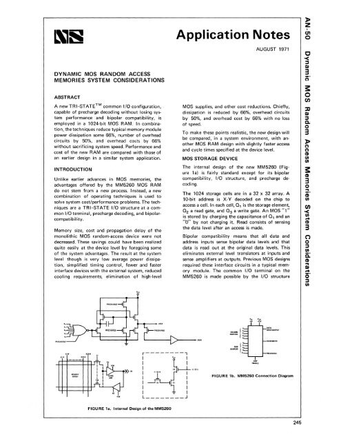
- Page 245 and 246: ...... oca...U)CDc::CD~...CD...()..
- Page 247 and 248: fo....ca ...CDCCDC!J...CD...Co)...c
- Page 249 and 250: ...eno...C1:I...Go)c::Go)C!)...Go).
- Page 251 and 252: n>coQ.rnCQ)>o~rn ...Q)1;)C)Q)a:....
- Page 253: en>caC.enCC!)>o~en""" C!)tienC!)a:T
- Page 257 and 258: U)co',f:to...G):2U)coCJEG)...U)>enU
- Page 259 and 260: enCo....ca...CI):EencoUECI)....en>e
- Page 261 and 262: enECD;>en"0~cao.c>CD~CCD(,)...ca~CD
- Page 263 and 264: enECD....en>tJ)"C...~o.c>CD~c:CDCJ~
- Page 265 and 266: nE...CDrn>UJ"C-cao.Q>CD~CCDCJca....
- Page 267 and 268: enEQ)...en>en..."CcooJ:l>Q)~r:Q)(,)
- Page 269 and 270: U)EQ)...U)>til..."0coo.c>Q)~c- ...Q
- Page 271 and 272: enECI)...en>en"C...C'CSo.Q>CI)~c:CI
- Page 273 and 274: ...enQ)...enC)Q)a:...0f-.&:.tJ)()Ec
- Page 275 and 276: ...(1)Q)....(1).-0>Q)a:........s::.
- Page 277 and 278: ..... oCO..Q)..Q)...CJco ..U)cQ)oco
- Page 279 and 280: (I)..... oasQ)..Q)...Co).. asas..cQ
- Page 282 and 283: BriefsJANUARY 1970...aTRIG FUNCTION
- Page 284 and 285: MASK PROGRAMMING SPECIALIZESMOS SHI
- Page 286 and 287: ORDERING INFORMATIONWhen ordering,
- Page 288 and 289: Clock Repetition Rate: The range of
- Page 290: National Semiconductor Corporation2