Download Issue - Chip Scale Review
Download Issue - Chip Scale Review
Download Issue - Chip Scale Review
- No tags were found...

You also want an ePaper? Increase the reach of your titles
YUMPU automatically turns print PDFs into web optimized ePapers that Google loves.
JF MICROTECHNOLOGY SDN BHDBring Possibilities .\WeExplore thesenew exciting andoutstanding solutions onour website or with our nearestsales channel partner today.Find out more at:Or e-mail us at:<strong>Chip</strong> <strong>Scale</strong> <strong>Review</strong> May/June 2013 [<strong>Chip</strong><strong>Scale</strong><strong>Review</strong>.com]5
MARKET TRENDSMemory Packages Adapt to Demand ShiftsBy Jim Handy [Objective Analysis]The ballooning bandwidthrequirements of today’sprocessors are beingdealt with by increasing the number ofbuses feeding the CPU. Two buses andeven three-bus systems are becomingincreasingly common. What is notobvious is that the size of the memory inPCs is limited by economics: The PC’smain memory doesn’t double or tripleevery time a new bus is added, it hasto remain at the same size to be pricecompetitivewith lower-bandwidth PCs.The system satisfies its bandwidth needby using a larger number of packageswith very low density (i.e., inexpensive)chips inside. This causes lower-densityDRAM chips to remain in the marketlonger than they have in the past. Asthe price of the lower-density chipsdecreases, the overall average sellingprice (ASP) of DRAMs slides (Figure1) putting phenomenal pressure on theprice of DRAM back-end processes(package and test) as these two elementscontribute to an increasing share of thetotal cost of the memory system.Meanwhile, the opposite has beenoccurring in the second-biggestmemory market – NAND flash. Theaverage memory size of NAND flashapplications has been increasing fasterthan the density of the chips in thesesystems, yet the form factor of thesystem (whether a phone handset orother mobile device) has been steadilyshrinking. Thanks to these twoconflicting trends, NAND flash makershave had to stack chips in increasingnumbers to satisfy consumer demandfor mushrooming flash capacities inshrinking product form factors. Twochipstacks, which were uncommon asrecently as 2000, have been supersededby 4-die and 8-die packages. Although16-die packages ship today, the 8-diestack is the tallest stack currentlyshipping in volume, but that mightchange over the next few years.Naturally, since these are consumerproducts, there is significant pressureto keep prices down. NAND makershave found a way to drive all of thecost out of these stacked parts, thanksto a lot of challenging work performedby packaging engineers. I find itamazing that an 8-highstack of 16Gb NANDdice commands no pricepremium over eightindividually-packaged16Gb NAND chips, orfour 2-die stacks, or eventwo four-chip stacks. Inflash cards, such stacksnow very commonlyinclude eight NAND chipsplus a controller.All this has been givena more pronounced impactby the fact that buyersappear to be putting offPC purchases in favor ofmobile devices such assmart phones and tablets.Mobile devices, in turn, are usuallyNAND rich and use only the smallestDRAM. The market is undergoingimportant changes that will create evengreater turmoil for chip makers thanthey have witnessed in the recent past.Today’s technologies have gone aboutas far as they can, though. SixteenlayerNAND stacks have low yieldsthat cannot reach price parity with8-chip stacks. Today’s DRAM packagescan’t support significant increases insignal frequencies and the addition ofbuses multiplies the capacitive loadingon the processor and drives up powerdissipation. The market will have toundergo a revolutionary conversion overthe next few years.The shifts the market has recentlyundergone pale in comparison withwhat’s coming up. Some excitingnew packaging technologies are beingdeveloped that will provide morebandwidth and denser products whileFigure 1:DRAM average selling price is steadily decreasing.the market for these chips will beundergoing very dramatic changes.Let’s see what is ahead in the world ofmemory packaging.What Does the Future Hold?Three important emerging trends willdrive even more extreme packagingover the longer term: 1) Through-siliconvias; 2) Hybrid Memory Cube; and 3)NAND adoption in PCs. Let’s examine6<strong>Chip</strong> <strong>Scale</strong> <strong>Review</strong> May/June 2013 [<strong>Chip</strong><strong>Scale</strong><strong>Review</strong>.com]
<strong>Chip</strong> <strong>Scale</strong> <strong>Review</strong> May/June 2013 [<strong>Chip</strong><strong>Scale</strong><strong>Review</strong>.com]7
each of these in turn.Through-Silicon Vias. Throughsiliconvias, or TSVs, hold the promiseof simplifying inter-chip bondingfor stacked dice. It’s not difficult tounderstand that the sheer complexity ofbonding a 16-die stack using bondingwires alone poses great manufacturingchallenges that lead to yield losses.By moving to TSVs, all wire bondingof the upper chips can be eliminated,and this is expected to significantlyimprove yields for die stacks ofincreasing heights.Although today TSV technologyis not widely used, and presents newchallenges of its own, the same was trueof the standard 2-die MCP (multichippackage) in the middle 1990s. This isa technology that should mature anddevelop to drive out all cost and yieldchallenges over time. It is unclear howhigh of a stack can be economicallymanufactured using TSV technology– we may see stacks of 100 chips ormore over the long term. Imagine theimpact this will have on the density of aNAND package.Hybrid Memory Cube. Since theTSVs mentioned above can be used forinter-chip signaling that doesn’t needto exit the package, chip designerscan design I/O pins that don’t have todrive a PC board trace or be handledduring board assembly. This meansthat high-speed drive transistors canuse low currents (making them muchsmaller than today’s I/O transistors),and that there does not need to bespace-consuming electrostatic discharge(ESD) protection on these I/O pins.In addition, the TSVs replace bulkybonding pads, further reducing the sizeof the chip’s I/O.The inventors of the hybrid memorycube (HMC) took this opportunity todrive an architecture that is likely to beadopted in all higher-end computingsystems over the longer term. TheHMC stacks a number of DRAM chipsatop a logic die; the logic die is the onlychip that communicates external to thepackage. This means that this is theonly device that must have high-currentdrive transistors with ESD protection.Furthermore, it is manufactured usinga logic, rather than a DRAM, process– DRAM processes aren’t good atdriving high currents, so high-currentDRAM transistors are much largerand more expensive than their logicprocesscounterparts.But there’s more to the story!Because the I/O drivers on the DRAMchip are now much smaller than thoseof a standard DRAM, there can be moreof them without penalizing die area.Without large high-current transistors,ESD protection, or bonding pads, theseI/Os are so small that today’s HMCprototypes use thousands of DRAMI/O pins to communicate between theDRAMs and the logic chip, increasingbandwidth substantially.The HMC uses a point-to-pointexternal signaling interface tocommunicate with the processor. Thisgives the system designer considerablymore control over bus capacitance thanexists in today’s DIMM-based systems,and this capacitance is also much lower.This allows the bus to be run at vastlyhigher frequencies than can be donein today’s systems, which should helpthe memory keep up with the everacceleratingprocessor bus. Over time,Objective Analysis anticipates that theHMC could be used for all DRAM inPCs and servers.NAND Adoption in PCsIn 2011, Objective Analysispublished a report: “How PC NANDwill Undermine DRAM.” Through aseries of nearly 300 benchmarks wefound that (after a certain minimumsize DRAM was achieved) one dollar’sworth of NAND flash improved a PC’sperformance more than one dollar’sworth of DRAM. This is somethingthat the IT community has known foryears. Data center managers routinelyuse solid-state drives (SSDs) as a wayof reducing their DRAM requirements,cutting both cost and energyconsumption at the same time.Although PCs have not yet adoptedthis trend, it will occur over time, withDRAM main memory sizes stagnatingand new NAND dual in-line memorymodules (DIMMs) replacing thesmaller SSDs now commonly seen inUltrabooks. Users who wish to improvetheir system’s performance will simplyupgrade their NAND DIMM. As thishappens, DRAM will migrate awayfrom a removable format and will besoldered down. The HMC is very likelyto become the standard way in whichDRAM is built into the PC. DRAMwill become a cache to the NANDmain memory.SummaryWe have seen important changes inmemory packaging technology, movingfrom single-die packages to multiple-diepackages in NAND while experiencinga shift from low package counts tohigh package counts in DRAMs.Both have put significant pressureon packaging costs that have led toimportant innovations.Although we are now approachingthe limits of today’s technologies,new approaches in the form of TSVsand the HMC, are on the horizon thatshould move us well past today’s limitsallowing packaging advances to propelthe two disparate goals of increasingbandwidth for DRAMs while increasingNAND flash package density faster thanMoore’s Law supports.AcknowledgmentUltrabook is a trademark of Intel.BiographyJim Handy received his Bachelor’s inElectrical Engineering from Georgia Techand an MBA from the U. of Phoenix; heis a Director at Objective Analysis; emailJim.Handy@Objective-Analysis.com.8<strong>Chip</strong> <strong>Scale</strong> <strong>Review</strong> May/June 2013 [<strong>Chip</strong><strong>Scale</strong><strong>Review</strong>.com]
40 + years ofAnd now, the perfect nameTMQi•nex [kuh-nekts] 1. Over 40 years ofreliable burn-in and custom connections;2. Quality interconnects for nex-gen solutions.Introducing Qinex, thenew brand name forsuperior interconnectionsolutions from SensataTechnologies. Qinex, thenew word in perfectpitch.QUALITY. High-value interconnectionsolutions since 1970.• 24/7 global engineering• 24/7 global support teams• Local engineering and sales• Six Sigma quality management• Proven, reliable high-volumemanufacturing• Expert molding, design, andcustomizationINNOVATION. More I/O choices,smaller form factors, superiorperformance in less time.• Latest 3D design tools• On-site model shops• Rapid prototyping• Advanced thermal analysis• Design on demand• Broad range of innovativecontact designsPARTNERSHIP. In a fierce globalmarket, only Qinex reliably supportsthe innovation, reputation andcompetitiveness of your business.We’ll work with you to get it right,the first time.40+ years of perfect pitch.And now, the perfect name.WEB www.qinex.comEMAIL qinex@sensata.comCALL 1-508-236-1306<strong>Chip</strong> <strong>Scale</strong> <strong>Review</strong> May/June 2013 [<strong>Chip</strong><strong>Scale</strong><strong>Review</strong>.com]9
GUEST EDITORIALSystems Scaling for Smart Mobile SystemsRequiring a New Packaging PlatformBy Prof. Rao R. Tummala [3D Systems Packaging Research Center, Georgia Institute of Technology]Transistor scaling, startingwith the invention ofthe transistor in 1947,made electronics the largest single$1.5T global industry serving avariety of individual industries thatspan computing, communications,consumer, automotive, bioelectronicsand others. The basis for this industryis a result of singular focus in transistorscaling, leading to a 5B-transistor chip,involving dozens of semiconductorcompanies around the globe. But theelectronics landscape is changingdramatically, driven by a new industrythat integrates all these individualindustries into so-called “smart mobilesystems” and promises to perform everyimaginable function in the smallestsize and lowest cost that almost everyglobal person could afford. Sucha new frontier, however, requiresrevolutionary technologies referred to assystem scaling, in contrast to transistorscaling during the last 60 years. Smartmobile systems are expected to driveunparalleled electronics technologyparadigms in system miniaturization,functionality, and cost. These systemscaling technologies are many thatneed to be explored, developed,integrated, interconnected, tested andmanufactured. These include newelectrical, mechanical and thermaldesigns, new system substrate materialsand processes, integration of ultra-thinactives, ultra-thin passives, miniaturizedand innovative thermal structures, thinfilmpower storages such as batteries,and interconnections between all ofthese. Figure 1 illustrates the currentsize scale in millimeters, showing theFigure 1: System scaling gap from transistor scaling at 20nm node tosystem scaling to 100mm size.10 6 gap between transistor scaling andsystem component scaling.System Scaling Vision of SmartSystemsThe Georgia Tech PRC vision is toexplore system scaling technologiesfrom current milli- to- micro-scale in theshort term and to nano-scale in the longterm, thus providing a revolutionarypath to milli- to- mega-functional smartmobile systems, as implied in Figure 2.Figure 2: System scaling vision from milli-to mega-functional smart systems.Such advances will leadto unparalleled circuitand system functionsthat range from digital,analog, power, RF,wireless healthcare,bio, MEMS andnetwork sensors.Current hardwareapproaches involvepackaging of individualand stacked ICs thatrange from processors,memory, RF, MEMSand sensors as well aspassive components and batteries. Whilesome of these are packaged as twodimensionalMCMs and 3D wire bondand stacked packages, there is verylittle system scaling. As such, mobilesystem companies see an eventual limitto functionality driven by the thicknesslimit of about 6000µm, as shown inFigure 3. Such a limit doesn’t allowother functions requiring other ICsto be added. This limit can be largelyeliminated by changing the currenthardware platform thatinvolves packaging ofICs on flexible or rigidorganic packages andorganic system boards,which present fourmain limitations forsmart systems of thefuture: 1) I/O pitch toless than 50µm withlithographic groundrules below 5-10µmline lithography, 2)thermal performance, 3)mismatch in temperature10<strong>Chip</strong> <strong>Scale</strong> <strong>Review</strong> May/June 2013 [<strong>Chip</strong><strong>Scale</strong><strong>Review</strong>.com]
Figure 3: Functionality limited by thickness of current system scalingtechnologies (Courtesy of Qualcomm).coefficient of expansion (TCE)-driven,and moisture-driven reliabilities, and4) warpage, as these organic packagesare miniaturized in thickness below100µm, as ultra-thin packages. TheI/O pitch and line lithography limitationstresses on both theinterconnectionsand the ultra-low-kon-chip dielectrics.The warpage is dueto many factorsincluding lowmodulus. Inorganicpackages madeout of glass orsilicon address allthese fundamentalproblems and thusextends I/O pitchmuch below 50µm toas much as 10µm. The new generationSummaryGeorgia Tech proposes to offer anindustry consortium, involving the entireglobal chain for R&D and manufacturing,with a focus on many system scalingtechnologies that include the electricaldesign of glass, silicon and organicinterposers for power, signal, noiseand bandwidth, mechanical design forwarpage and reliability, panel–basedlow cost glass, organic and polysiliconinterposers and packages, 2-5µm largearea lithography and wiring layers, 10-30µm pitch off-chip and low temperatureCu-Cu interconnections, silicon, organicand glass package-to-board level surfaceFigure 4: Area array I/O pitch of a) current organicpackages at 120µm pitch and b) low TCE organicsat 50µm pitch.is a result of via on top of via misregistrationfrom layer to layer due tothe visco-elastic nature of polymers asthese are processed at or above theirglass transition temperature and thus areexpected to be limited to about a 50µmarea array pitch, as shown in Figure 4.The thermal conductivity of polymersis about two-three orders of magnitudeless than silicon. The mismatch in TCEbetween Si and organic is huge, creatingFigure 5: I/O pitch need and organic vs. inorganic regimes for emerging 2.5D and 3D packages(Courtesyof Globalfoundries).of low TCE organic laminates, however,offer an opportunity to extend the I/Opitch from 225µm pitch in 1987 to theircurrent value at 120µm pitch and, in thenear future, to about 50µm pitch. Figure5 shows two regimes therefore, one withextending flip-chip with organics, andthe other with inorganic platforms inextending I/O pitch to new levels, muchbelow 50µm. These can be combinedappropriately and selectively with ultrathinand special component technologiesmade of polymers for dielectrics,liners and stress-relief members; nanomagneticsfor antennas and powercomponents and ultra-high surface areaelectrodes, along with high-permittivitydielectrics for capacitors.mount technology (SMT) assembly, 3Dglass photonics, 3D integrated passiveand active components, among others.Georgia Tech’s PRC involves about 20cross-disciplinary faculty and dozens ofgraduate students.BiographyRao R. Tummala received his PhDin Materials Science and Engineeringat the U. of Illinois and is the JosephM. Pettit Endowed Chair in Electricaland Computer Engineering and theDirector of the Packaging ResearchInstitute at the Georgia Instituteof Technology. He was an IBMFellow prior to Georgia Tech; emailrao.tummala@ece.gatech.edu<strong>Chip</strong> <strong>Scale</strong> <strong>Review</strong> May/June 2013 [<strong>Chip</strong><strong>Scale</strong><strong>Review</strong>.com]11
INDUSTRY NEWSSEMI Europe Networking Day toFocus on Embedded PackagingTechnologiesSEMI Europe announced a newNetworking Day focusing on embeddedpackaging to be held on June 27, 2013in Portugal. Hosted by Nanium, in Vilado Conde (Porto, Portugal), the eventwill feature speakers from companiesinvolved in fan-out wafer-levelpackaging (FO-WLP) and in embeddeddie in laminate substrate.Driven by consumer markets andmainly by smartphone products,embedded packaging solutions providethe best power, performance, and areasystem tradeoff by integrating morefunctionalities into a smaller and thinnerpackage. With annual growth forecast atmore than 25% by market analyst firmssuch as Yole Développement, thesetechnologies are already implementedin high-volume cellular phonesand are critical for enabling futureinnovative solutions, including 3Dpackaging solutions.The Networking Day will combinepresentations from companies thatinfluence the industry and offer uniqueadd-ons such as the visit of Nanium’sclean room, the largest FO-WLP300mm facility worldwide, and severalnetworking opportunities includingthe Speed Networking Session andsocial evening events. Speakersfrom ASE Group (Taiwan) andSTMicroelectronics (Switzerland) willkeynote and share the latest results oftheir work in embedded packaging andtheir respective strategies. ASE Groupwas a very early adopter of the firstgenerationof FO-WLP (licensed eWLBtechnology developed by Infineon),starting with 200mm capabilities, andnow very active in embedded die insubstrate. STMicroelectronics, one ofthe founding members with Infineon andSTATS <strong>Chip</strong>PAC, of an R&D alliancein Singapore to advance the eWLBplatform back in late 2009, developeda wide range of technology optionsaround FO-WLP to serve its variousproduct groups addressing multiplemarket segments.Presentations from TechSearch(USA) and Yole Développment(France) will describe the technologylandscape, market and main players.Additional speakers from Intel MobileCommunications, AT&S, and NXPare confirmed.“We are pleased that we developedsuch a strong lineup of speakersfrom the main players designing,manufacturing and selling embeddedpackages all over the world,” saidHeinz Kundert, SEMI Europe President.“We are still at an early stage, manyadditional business opportunities inembedded packaging are still upfrontfor equipment and materials companies.Embedded packages have the potentialto become the new packaging platformbeyond the BGA solution.”The full event program is online andregistration is open. Anyone involvedin advanced packaging is invited toregister. The Networking Days area SEMI Europe initiative to supportstart-ups, SMEs, laboratories and largecompanies and to get “up to date” onhot topics that appeal to people acrossthe semiconductor supply chain. SEMINetworking Days, held on a quarterlybasis in industrial sites, are primeevents to connect with the people whoinfluence the industry and to initiatepreliminary partnership and businessrelationships. The Networking Days areopen to anyone and free of charge forSEMI member companies. For moreinformation about the event, please visitwww.semi.org/eu/node/8481 or contactYann Guillou in the SEMI EuropeGrenoble Office (yguillou@semi.org).SEMI: Memory, Foundry, and LEDMarkets Drive Fab Spending inSoutheast AsiaIn early April, SEMI reported thatincreased spending in NAND andflash by Micron, LEDs by Philips andOsram, and continued investmentsby Globalfoundries, will create newopportunities for equipment andmaterials suppliers in Southeast Asia.The trade group noted that, for theSoutheast Asia region, capital equipmentinvestment will see some pickup inthe second half of 2013 followed bya strong recovery in 2014. Overall,front-end fab equipment spending isexpected to double next year from $810million in 2013 to $1.62 billion in 2014.Foundry and memory are the two majorsectors that invest most in the region.The Globalfoundries expansion plan atFab 7 will be completed by mid-2014,while UMC continues to upgrade itsFab 12i capacity to the 40nm process.The Southeast Asia region’s capacitygrowth for front-end fabs shows a 2%increase this year and an expectation ofhigher growth, 8%, in 2014, exceedingoverall global capacity growth of 5%according to the SEMI World FabForecast. The growth will mainly bedriven by memory sector, specificallyfrom NAND flash capacity as Microngears up for further expansion at itsSingapore NAND flash facility nextyear, plus ongoing capacity conversionfrom DRAM to NAND flash at Fab7 (Tech). Singapore is emerging tobecome the third largest NAND flashmanufacturing country in the world bythe end of 2014. The conversion andthe expansion projects will drive relatedsemiconductor investment in the regionin 2013 and 2014.For the assembly and test sector,Southeast Asia has long been thefocal point of the industry with a largeinstalled capacity from both IDMs and12<strong>Chip</strong> <strong>Scale</strong> <strong>Review</strong> May/June 2013 [<strong>Chip</strong><strong>Scale</strong><strong>Review</strong>.com]
OSATs. This position contributes tothe region being the largest packagingmaterials consumption market in theworld, representing a market size of$6.6 billion in 2013 and $6.8 billion in2014. The region’s back-end equipmentinvestment remains significant withover $1 billion spending each yearthroughout 2012 to 2014, accountingfor about 17% of worldwide shareaccording to SEMI’s WWSEMS.Aside from manufacturing capacity,the Southeast Asia region is nowextending its value proposition to ICdesign and R&D areas with more jointdevelopment projects between multinationalcorporations (MNC) and localinstitutes. SEMI expects to see a morerobust semiconductor ecosystem arisefrom the region as a result of theseendeavors and as companies seek readyaccess to customers throughout Asia-Pacific and South Asia.Currently, Singapore has 14 waferfabrication plants, including the world’stop three wafer foundries. Singaporealso has 20 semiconductor assemblyand test operations, including three ofthe world’s top six outsourced assemblyand test companies. There are about40 IC design centers that comprisenine of the world’s “top 10” fabless ICdesign companies.Imec Reports 6.7% Growth for 2012Fiscal Year EndImec reported financial resultsfor fiscal year ended December 31,2012. Revenue for 2012 totaled 320million euro, a 6.7% increase from theprevious year. The 320 million eurofigure includes the revenue generatedthrough collaborations with more than600 companies and 200 universitiesworldwide, a yearly grant from theFlemish government totaling 48.2million euro, and a 8.2 million eurogrant from the Dutch governmentto support the Holst Centre. “Wecontinued to expand and renew ourR&D partnerships on semiconductortechnology scaling, as well as on newemerging areas such as the biomedicalfield,” said Luc Van den hove, CEO ofimec. “Our robust growth last year is atestament to the strength and value thesepartnerships add to the developmentof next-generation technology andits applications.”In 2012, imec’s talent base grewto 2,051 people, representing 75nationalities. Of these, 377 wereresidents, visiting researchers from<strong>Chip</strong> <strong>Scale</strong> <strong>Review</strong> May/June 2013 [<strong>Chip</strong><strong>Scale</strong><strong>Review</strong>.com]13
partner companies and institutes, and276 were PhD researchers. One-hundredtwenty-two employees are based atthe Holst Centre, an open-innovationinitiative between imec and TNOlocated in Eindhoven, the Netherlands.“Given the current challengingeconomic backdrop, I am thrilled withthe steady growth we have realizedthe last two years,” said Van den hove.“Thanks to the efforts and talent of ouremployees, as well as the strength ofour strategic research partnerships, weachieved significant breakthroughs in allour research areas.”Among the highlights of the 2012R&D report include: 1,064 peerreviewedarticles published, 161 patentsawarded, 133 patent applicationssubmitted, and the successful renewalof the IOS9001 quality certification.Yole Développement <strong>Issue</strong>sForecasts in MEMS and Glass WafersRecent forecasts by YoleDéveloppement covered the MEMSpressure sensor market, and the glasswafer market:MEMS Pressure Sensor MarketAfter years of limited growth,Yole Développement reported thatthe MEMS pressure sensor market isgrowing due to consumer electronicapplications and is expected to showa 22% CAGR. Pressure sensors areplaying an important role today inmodern industries. MEMS pressuresensors are already widely adopted indifferent applications for their highperformance,low cost and small size.In its new report “MEMS PressureSensor,” Yole Développement givesa detailed overview of the MEMSpressure sensor markets, technologiesand players. This report details the mainapplications in automotive, consumer,medical, industrial and high-endsegment, and the main players in theindustry. It also analyzes the currentpressure sensor technologies includingMEMS technologies, and gives adetailed MEMS pressure sensor marketforecast by application.Emerging consumer applicationsare boosting the growth of the MEMSpressure sensor market and reshufflingthe main playersThe MEMS pressure sensor is oneof the very first MEMS componentsappearing in the microsystem world.The technologies are quite mature andthe market is big and expected to growfrom $1.9B in 2012 to $3B in 2018(Figure 1). “The MEMS pressure sensorfor consumer applications, especiallyfor smartphones and tablets, isfollowing the model of accelerometersand gyroscopes. Adoption of this modelwill help the MEMS pressure sensormarket to boom again! We believe,this huge opportunity will result in theglobal volume of the MEMS pressuresensor market hitting 2.8 billion unitsby 2018,” announced Wenbin Ding,Technology & Market Analyst, MEMSDevices & Technologies at YoleDéveloppement. “Consumer pressuresensors will represent 1.7 billion unitsand will overtake automotive as themarket leader in volume,” she added.Even though the consumer applicationhas a much lower ASP than otherapplications, this promising segmentFigure 1: MEMS pressure sensor market forecast by applications 2012-2018.SOURCE: MEMS Pressure Sensor report, April 2013, Yole Devéloppement.will bring more than 8% CAGR to theglobal MEMS pressure sensor market.The report consolidated market data for2012 and provides forecasts until 2018.Automotive applications are stilldominating the MEMS pressure sensormarket. TPMS, MAP and BAP willbe the biggest sub applications in thisfield, noted Yole. Automotive, medical,industrial and high-end markets aregrowing 4% to 7%, however, theconsumer market is growing 25% invalue (38% in volume) because of newopportunities in smartphones and tablets.The MEMS pressure sensor findsnew applications in each domain, forexample: in-cylinder pressure sensingfor automotive, the CPAP (continuouspositive airway pressure) machine formedical use, smartphones (SamsungGalaxy Slll for indoor navigation) andtablets for the consumer electronicsindustry, etc. All these emergingapplications are still in their infancy,but they appear promising and YoleDéveloppement’s analysts believe theMEMS pressure sensor will find newways to satisfy end users in each domain.Glass Wafer MarketYole Développement recentlyannounced results from its glasssubstrates for semiconductormanufacturing report.The research firm notedthat over the last fewyears, glass has gainedconsiderable interestfrom the semiconductorindustry due to its veryattractive electrical,physical and chemicalproperties, as wellas its prospects fora relevant and costefficientsolution. Theapplication scope ofglass substrates in thesemiconductor fieldis broad and highlydiversified. End14<strong>Chip</strong> <strong>Scale</strong> <strong>Review</strong> May/June 2013 [<strong>Chip</strong><strong>Scale</strong><strong>Review</strong>.com]
applications include: MEMS, CMOSimage sensors, LED, memory and logicICs, RF/analog ICs, power, microbatteries,optoelectronic components,and microfluidics. Functionalitiesinclude support substrate,WLCapping, 3D through-glass via(TGV)/2.5D interposer, carriers, andmicro-structuring.Mainly driven by the wafer-levelpackaging industry, Yole expects theglass wafer market to grow from $158Min 2012 to $1.3B by 2018, at a CAGRof ~41% over the next five years (Figure2). “Initially driven by CMOS imagesensor and MEMS applications, thisgrowing industry will be supported byrelevant end-applications such as LED,memory and logic IC, where glass ison its way to being commercialized,”said Amandine Pizzagalli, Marketand Technology Analyst, Equipment& Materials Manufacturing, at YoleDéveloppement. “In terms of wafersshipped, a 4X glass wafer growth isexpected in the semiconductor industryover the next five years, achieving morethan 15M 8” EQ [wafer starts per year]WSPY by 2018.”The glass WLCapping platform is amature functionality already adoptedwith significant volume in CMOSimage sensors, where more than 3.3Mglass caps were shipped in 2012. Thismarket is expected to grow slowly,with a CAGR of 14% from 2012-2018,mainly supported by MEMS devicesimpacted by the request for furtherminiaturization. On the flip side, theglass market for WLOptics will likelydecline from 2015-2018 because of thedevelopment of competing technologies.Despite the above considerations,Yole expects to see strong growth inthe glass market, mainly supported bytwo emerging WLP platforms: with aCAGR of 110% and 70% respectively,the glass-type 2.5D interposer emergingplatform and the carrier wafer will beglass’s fastest-growing fields over thenext five years, because glass offersthe best value proposition in terms ofcost, flexibility, mechanical rigidity andsurface flatness.If glass is qualified for 2.5Dinterposer functionality, the glassmarket could exceed $1B in revenueby 2018. However, it’s still unclearhow back-end-of-line (BEOL) waferfabs will choose glass over the currentsilicon technology used for logic ICapplications (for the 2.5D/3D systemon-chip(SoC) and system partitioningareas), but the glass variety of 2.5D(continued on Page 46)PHOTOLITHOGRAPHYFOR TSV AND 3D-ICEVG ® 150 Resist Processing SystemConformal Coating in Vertical ViasExposure with Proximity LithographyIn-Via Resist DevelopmentGET IN TOUCH To Discuss Your Manufacturing Needs: www.EVGroup.comVia processed on EVG ® systems<strong>Chip</strong> <strong>Scale</strong> <strong>Review</strong> May/June 2013 [<strong>Chip</strong><strong>Scale</strong><strong>Review</strong>.com]15
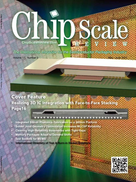
Realizing 3D IC Integration with Face-to-Face StackingBy John Xie [Altera Corporation] and Deborah Patterson [Amkor Technology, Inc.]Semiconductor processscaling, as driven byMoore’s Law, hasbeen the key driving force behindthe evolution of today’s high-techindustry. But increasingly, traditionalprocess scaling alone can no longermeet system performance, throughputand power requirements. Althoughside-by-side monolithic silicon (2Dstructures), package-on-package(PoP), and package-in-package (PiP)platforms allow for two or more chipsto be bonded together, they do not offerenough density, bandwidth or powerto meet the requirements of nextgenerationproduct roadmaps.The trade-offs between placing morefunctions on a chip (system-on-chip,SoC) versus placing more functionswithin a package (multi-chip package,MCP, or system-in-package, SiP) mustbe fully evaluated. Optimizing overallperformance as well as total cost-ofownershipare equally important. Andperhaps one of the most significantissues is accelerating time-to-market, asit is a strategic enabler to the end users.To properly assess the above tradeoffsin terms of effective silicon usagevis-à-vis functional integration (nodeoptimization), die yield considerationsfrom ramp to production, and theinfluence of the packaging strategy onsignal integrity − ideally the packagewould be invisible to the signal whileproviding protection, thermal dissipation,etc. − both 2.5D and 3D packaging arebeing actively investigated.An example of a 3D integrated circuit(IC) is represented by stacked ICs withthrough-silicon vias (TSV). In a 3D ICstack, solder bumps are used to join onedie on top of another to allow the signalsto travel between the die. 3D IC stackscan be packaged independentlyor can be connected side-bysideon a substrate to otherICs. A 2.5D IC package, incontrast, is defined by the useof a multilayer passive siliconinterposer as a substrate tointerconnect multiple activedie or die stacks in a sideby-sideconfiguration. TSVsare used to route the signalsthrough the silicon interposerdown to flip-chip solder bumpslocated on the interposer’sbottom side. The ICs themselvesuse much smaller copper (Cu) pillarmicro-bumps for assembly onto thesilicon interposer.Using silicon as a platform forinterconnecting the active ICspreserves signal integrity far betterthan conventional substrate materialsand, in fact, enables new ways ofthinking about SoC versus MCP tradeoffs.The 2.5D package offers silicongradeinterconnect density and greatlyreduced signal latency because of theshort interconnect path between theactive silicon die. Power consumptionis also reduced because of I/O driversthat can be designed with Si-Si directinterconnect and reduced Joule loss onthe interconnect path. 2.5D stacking alsohas a time-to-market advantage because3D ICs require longer lead times toimplement design and manufactureat the component level, and then tocoordinate their concurrent assembly.The performance advantages of stackedICs are illustrated in Figure 1, whichcompares the relative interconnectdensity, thermal resistance, and powerusage between monolithic, 2.5D, and3D IC packages.The advantages of 2.5D stackedFigure 1: Comparison of the relative interconnect density, thermalresistance and power usage between three types of stacked multichippackages.packaging have ushered in a newmindset on how to approach SoC versusMCP packaging and their combinedimpact upon near- and long-term siliconand package functional integrationroadmaps. Aside from 2.5D and 3Dsemiconductor packaging approaches,there are still other innovative waysto increase function and performancewhile keeping package footprints smalland supporting time-to-market goals.Realizing that an optimized stackingconfiguration, coupled with a properdesign and manufacturing flow canenable a relatively low cost stackedstructure, Altera Corporation and AmkorTechnology collaborated on the projectroadmap for functions: for example,whether to use an SoC, or to re-architecta device, separating it into pieces toincrease die yield.Introducing an ‘About Face’Stacking innovation is a key focus formany semiconductor suppliers as wellas packaging and assembly companies.Altera’s internal R&D organizationhas produced a five-year roadmap forstacking technology. Similarly, Amkor’sadvanced development team supportsnumerous stacked manufacturing and16<strong>Chip</strong> <strong>Scale</strong> <strong>Review</strong> May/June 2013 [<strong>Chip</strong><strong>Scale</strong><strong>Review</strong>.com]
assembly approaches involving bothwire bond and flip chip solutions.A “face-to-face” packaging approachrepresents one type of stacked chipon-chip(CoC) arrangement. Two dieare joined face-to-face through copperpillar micro-bumps in order to make theconnection between the active circuitryon each die closer - without havingto add any TSV processing. One diemust be sufficiently larger than theother (mother) such that all of its dieto-substrateflip-chip bumps are placedaround the larger die’s perimeter, withthe smaller die (daughter) attachedinside. The daughter die and its bondedCu columns must be thinner than thecollapsed flip-chip bumps surroundingit, to ensure sufficient clearance betweenit and the next assembly surface. Figure2 illustrates an example of this structure,dubbed the POSSUM packageconfiguration by Amkor.Figure 2: Illustration showing a face-to-face chipon-chipassembly that brings the active circuitryon each IC as close as possible without the useof TSVs. The larger die (mother) is assembled tothe BGA substrate through flip-chip solder bumps(shown) or Cu pillar bumps/posts and the smallerdie (daughter) is joined to the mother die throughcopper pillar micro-bumps.The key feature of this packagingstyle is that it bonds two active ICsdirectly using Cu pillar micro-bumpswithout the need for TSVs or a siliconinterposer. In fact, the structureuses established flip-chip substrateand assembly technology. It offersalmost all of the true 3D IC stackingadvantages: the stacked chips talkdirectly to each other with reducedlatency, better signal quality, andadditional power savings as comparedwith a 2.5D structure. The footprint isreduced and the stack does not growin the Z-axis. Integration cost is alsomuch lower than in 2.5D stacking. Theface-to-face flip-chip structure alsonegates the complicated design and highmanufacturing costs associated withintegrating TSVs into active silicon.Face-to-face stacking offers severalpackaging options. In addition to face-to-face flip-chip chip scale package(CSP) or ball grid array (BGA)packaging, lead frame packaging hasalso been demonstrated (Figure 3).Face-to-face PBGA represents the mostadvanced of these packages as it utilizesa POSSUM mounted die assembledto the face of a larger die.Figure 3: Illustration of three different face-to-face chip-on-chippackage configurations.Circumventing the Cost vs. DensityTrajectoryAs I/O density increases, the relativecost of packaging also increases. Figure4 sets as a baseline a typical 2D flipchipBGA (FCBGA) shown at the lowerleft corner of the chart. With a 100µmminimum I/O pitch and 10µm silicontrace width (which cannot be matchedoff-chip), the trend is toward an increasein cost as increasing I/O density andsmaller feature size progress. The finerpitches and line widthscharacterized by anultra-high density I/O(UHDI-O) device, andthat of the sub-50µmpitches that enable 2.5Dinterposer structuresconfirm the predictablecost progression.Against this backdrop,note that face-to-faceassembly, be it Cupillar flip-chip or wirebonded interconnect,deviates from this lineback toward a lowercost offering.Applications of Face-to-FaceStacking TechnologyThere are a number of semiconductorcombinations that will benefit from aface-to-face stacking approach. Forexample, a high-density FPGA maybe bonded with an ASIC to providea combination of ASIC performanceand FPGA flexibility ina specific applicationspace. Perhaps themost obvious use isto combine two dicefabricated in differenttechnologies, such as anRF front-end die and anFPGA die. Face-to-facebonding gives sufficientbandwidth between thetwo devices to allow fordirect digital interactionwith the RF circuitry.Similarly, bonding anFPGA to an externalmemory die can greatlyexpand the FPGA’s access to lowlatencymemory without incurringthe energy costs of high-frequencychip crossings.As system throughput demands andworking-storage bandwidths increase,the memory energy issue looms large.Figure 5 compares the switching powerneeded per I/O channel for differentmemory solutions. It shows that face-tofaceSRAM stacking offers essentiallythe same power and bandwidthadvantage as a true 3D IC stack.Figure 4: Illustration of packaged IC cost progression as I/O density increases.<strong>Chip</strong> <strong>Scale</strong> <strong>Review</strong> May/June 2013 [<strong>Chip</strong><strong>Scale</strong><strong>Review</strong>.com]17
Figure 5: Simulated data demonstrating that face-to-face assemblyof an SRAM onto an FPGA offers the same power and bandwidthadvantage as a 3D TSV stacked die structure (MLAB is referring toembedded memory or the SOC option).Nurturing a 3D PackagingAlternativeConsideration of the design andresponse of semiconductors and theirpackaging in parallel is important andgreatly influences downstream technicaldirection, especially when the designmust concurrently optimize total costof-ownership,product performance,and time-to-market. This awarenesssupports early partnering between theIC supplier and the OSAT (outsourcedsemiconductor assembly and test serviceprovider). This broad combination ofexpertise, resources and experience isrequired in identifying viable packagingtechnologies that support aggressiveproduct roadmap objectives.The face-to-face POSSUM packageprovides an example of this blendingof expertise. The structure was chosendue to its ability to join two or moredie with closer coupling for shorter,faster communication. Less inductance,cross talk and parasitic resistancemeant that the method was suitablefor high frequency, high bandwidthapplications. And the package wasbased on established process flows thatwere already in production, such as Cupillar micro-bumping, flip-chip solderbumping, chip-on-chip mass reflow and/or thermo-compression bonding, chip-tochipwire bonding, or chip-to-substrateflip-chip or wire bonding, as appropriate.In addition, the package could beramped to high-volume manufacturingwithout introducing complexwafer handling processes.Face-to-Face <strong>Chip</strong>-on-<strong>Chip</strong>AssemblyThe platform supportingCoC assembly is a directresult of the combination ofcopper pillar wafer bumpingknow-how and its advancedfine pitch assembly. Thespecifics of the bumping aretailored to the product designand assembly process flow.After the copper pillarmicro-bumps are applied tomother and daughter wafers,back grinding and dicingare performed. There is the optionto separate the mother die or for itto remain in wafer form, dependingon process flow optimization. Thedaughter die is then joined to themother die using Cu pillar microbumps.Various bump structures,interconnection materials and processesto control bump standoff (e.g., noncollapsiblecore) are being investigatedto provide for optimal reliability,electrical, and thermal performance. Cupillar micro-bumps are in high-volumemanufacturing at 40µm peripheral and80µm staggered pitch, and in lowvolumeproduction at 30µm peripheraland 60µm staggered pitch.Multi-Bump Height Flip-<strong>Chip</strong>ImplementationFor the current face-to-faceconfiguration, a taller Cu pillar microbumpis created on the daughter die anda shorter height bump is formed on thelarger mother die. Figure 6 illustrates aclose up of the concept where the dualsize bumps are joined between motherand daughter die.Note that the structure also utilizesFigure 6: Close-up view of the dual size copperpillar micro-bumps used to join the mother (top)and daughter (bottom) die in a face-to-faceconfiguration (not to scale).advanced dual height bumping for thelarger mother die. The CoC die padregion is bumped with the shorter bumpswhile the peripheral region outside theCoC bonding area is bumped with thetaller copper pillar micro-bumps.Assembling a 3D Package WithoutTSVsThere is a choice of two chip attachassembly processes for face-to-face Cupillar bonding. The first is mass reflowwith capillary underfill (MR+CUF),which is typically used for bump pitch>80µm with migration to >50µm.The second chip attach assemblyprocess is thermo-compression bondingwith non-conductive paste (TC+NCP).This process is currently used in highvolumemanufacturing production fordie with 40/80µm I/O pitch for die-tolaminatesubstrates and has been foundto be high yielding and reliable.The TC+NCP assembly processis employed to join the mother anddaughter ICs. Upon completion ofthis face-to-face assembly, the bondeddice are then attached to the substratethrough a mass reflow process. It iscritical to maintain a proper underfillflow that is uniform across the gapbetween the mother and daughter ICsin order to avoid the formation of airpockets after underfill cure. The processwas refined to ensure void-free underfilland proper gap collapse between themother and daughter die. Both variationof the die and substrate warpage aretaken into consideration. The assemblyof the devices onto the substrate is thenfollowed by lid attach, ball attach, lasermarking and test. Figure 7 shows across-section and various close up viewsof the assembled package.On-going development continuesto advance the sphere of influenceof chip-on-chip assembly. <strong>Chip</strong>-on-Wafer (CoW) processing, which utilizesequipment and process methods wherethe smaller die is attached directly tothe larger die while it is still in waferform, are in development. CoW alsoprovides for the support of wafer-levelchip scale packaging (WLCSP) withinthe POSSUM platform. Advances18<strong>Chip</strong> <strong>Scale</strong> <strong>Review</strong> May/June 2013 [<strong>Chip</strong><strong>Scale</strong><strong>Review</strong>.com]
Figure 7: Cross-section of a FPGA die (mother) with a thinned 60µm ASICdie below (daughter). The two devices are assembled face-to-face throughan array of 40µm Cu pillar micro-bumps. The ASIC is joined to the substratethrough thicker Cu posts + solder microballs at a pitch of 200µm.in materials across all 3D platforms aresimilarly adoptable to CoC applicationas they become available.Temperature cycle tests have beenconducted on packages using the Cu+ SnAg solder caps. The packageshave passed -55°C to 125°C for 2000temperature cycles (JESD22-A104D,Level B). Other packages using Nibumps + SnAg that are joined to Cupillar + SnAg have withstood -55°C to125°C for 3000 temperature cycles.3D IC integrationwith TSVs remainsan industry target,there are clever waysto address low-coststacking in the nearterm. Face-to-faceflip-chip packaging isexpected to producecomplex, highlyintegrated, andhigh performanceproducts for a vastarray of computing,communications,automotive andconsumer products.This is especiallyimportant for devices with theprogramming flexibility of FPGAswhere ever increasing functionality anddecreasing size and weight are required.AcknowledgementsThe authors would like to thank MJLee, Yuan Li, Zhe Li and the Alterapackaging R&D team in both San Joseand Penang, as well as Jemmy Sutanto,DongHe Kang, Michael Oh, Kwang-Seok Oh, KyungRok Park, Sa YunMa, Robert Lanzone, Dave Hiner, RonHuemoeller and their advanced productdevelopment teams from AmkorTechnology and Amkor TechnologyKorea for their joint contributions tothis project.BiographiesJohn Xie received his PhD inPhysics from the Chinese Academy ofSciences with post-doctoral researchat UC Berkeley and LawrenceBerkeley Labs; he is the Director ofPackaging Technology Research andDevelopment at Altera Corporation; emailjxie@altera.comDeborah Patterson received her BS inEngineering from the U. of California,San Diego and is the Sr. Director ofProduct and Technology Marketingat Amkor Technology, Inc.; emaildeborah.patterson@amkor.comSummaryUpstream concurrent IC and packagedevelopment allows for the assimilationof cost effective packaging solutionsthat optimize the right set of featuresin order to support the varied andaggressive requirements of end users.In a short period of time, the jointdevelopment team has made tremendousprogress on silicon bump design andmanufacture, substrate structure andprocess, and assembly BOM andmanufacturing flow. The team ispursuing several other types of stackingapproaches and their integration intoestablished packaging platforms (e.g.,from wire bond and flip-chip to BGAsand lead frames).The POSSUM configurationillustrates how face-to-face packagingcan be optimized to leverage highperformance in a multi-chip assemblywithout the use of expensive 2.5D or3D TSV constructions. Although fullSockets, Contactors & Adaptersfor Prototype Development & Test• Compatible with virtually any footprint• Probe-pin & Elastomer solutions• Pitch range from 0.30mm to 2.54mm• Pin counts up to 2000• Bandwidth to 40GHz• SMT, thru-hole & solderless options• Several socket closure styles available• Custom requirements are welcome• Competitive pricing• Expedited deliveryFor further information visit www.e-tec.comor contact us directly for immediate attentionE-Tec Interconnect Ltd, USA Marketing & SalesE-mail: info-US@E-tec.com, Telephone: +1 408.746.2800(www.e-tec.com)<strong>Chip</strong> <strong>Scale</strong> <strong>Review</strong> May/June 2013 [<strong>Chip</strong><strong>Scale</strong><strong>Review</strong>.com]19
Integrated Silicon Photonics Fabrication on a300mm PlatformDouglas Coolbaugh, Thomas N. Adam, Gerald L. Leake, Phung Nguyen, Michelle L. Pautler [College of Nanoscale Science and Engineering]Jonathan Bradley, Ehsan Hosseini, Michael Watts [Research Laboratory of Electronics, Massachusetts Institute of Technology]The College of NanoscaleScience and Engineering(CNSE) working incollaboration with the MassachusettsInstitute of Technology (MIT) hasdeveloped a full flow photonicsprocess on 300mm silicon-oninsulator(SOI) and bulk wafers.This offering encompasses multilevellow-loss silicon and siliconnitride waveguides, high speedgermanium detectors, and activeelectro-optical components that canbe co-integrated with advanced 65nmlow power CMOS base technologiesusing 3D integration (Figure 1).These derivatives were developed forintegrated photonic solutions and otheroptoelectronic applications. Stateof-the-artindustry-leading 193nmimmersion photolithography and afully equipped 300mm research fabenabled the successful incorporationof nanophotonic elements with highendCMOS base technologies and afully developed 3D integration process.Basic and advanced process flowswere employed for standard photonicsapplications in conjunction with CMOSFigure 1: Fully equipped 300mm CMOS and photonics cleanroom facilities.and 3D integration. In addition, researchlevel photonics can be modified forspecific customer requirements, andnovel materials and prototype devicescan readily be developed and tested.Integrated CMOS-compatibleWaveguidesIntegrated photonics circuits requirewaveguides that transport optical signalsbetween components on one chip aswell as on and off the chip. While signaldispersion can be neglected for theserelatively short distances, the lowestabsorption is needed to balance the lowdetector sensitivity and small opticalgain in on-chip amplifiers and sourcesof today. In addition, a wide range ofwavelengths (633nm to 1550nm) isneeded for specialized applications thatrequire guiding, mixing, or pumpingwith sources using shorter wavelengths.Most common integrated waveguidesand resonators are of rectangularor ridge geometry and fabricated insilicon (single- or poly-crystalline) orsilicon nitride. Single-level designsfor components test applications werebuilt using either silicon or siliconnitride as the waveguiding layer. Twoleveldesigns were implemented todetermine coupling efficiencies andtest modulators, switches, and opticallypumped components. Multiple-levelphotonics circuits were integrated withfull-build CMOS logic to demonstratefully functional opto-electronic circuits.Leading-edge 193nm immersionlithography with sub-60nm resolutionand advanced reactive ion-etchingwas used to pattern waveguides withminimal loading effects, negligibleinter-level misalignment, and nearlyperfect rectangular shape (sidewallangle of 90±1degrees). The residualsidewall roughness caused by lineedgevariations during the lithographyprocess as well as random geometricfluctuations stemming from reactiveionetching was eliminated using acombination of dose and focus offsets,tone reversal, and thermal and oxidation/etching processing. As depicted inFigure 2, sub-100nm features (gaps,holes, lines) were obtained withoutoptical proximity correction (OPC)while a resolution of 50nm and belowcan be achieved applying OPC models.Furthermore, advanced UV lithographyis available for printable features of20nm and below.Dielectric Waveguides. Traditionally,low-pressure chemical vapor deposition(LPCVD) nitride on top of micrometerthick thermal oxide was used inphotonics circuits owing to extremelylow losses in the visible and infraredspectrum [1]. However, co-integrationwith CMOS or bipolar circuitryis prohibitive due to the excessivethermal budget and consumption ofsilicon during oxidation. Therefore,combinations of low-temperature and20<strong>Chip</strong> <strong>Scale</strong> <strong>Review</strong> May/June 2013 [<strong>Chip</strong><strong>Scale</strong><strong>Review</strong>.com]
Figure 2: Features defined by immersion lithography without optical proximity correction. a) (Left) 95nmgap between waveguide and micro-ring resonator before softmask removal; b) (Right) 95nm silicon nitridewaveguide on buried silicon waveguide.low-loss deposited nitride and oxidehave become an attractive alternativethat allow logic-first co-integration.We have developed plasma-enhancedSi 3 N 4 waveguides fabricated onmicrometer thick plasma-enhancedtetraethyl orthosilicate SiO 2 (pTEOS)cladding with processing temperaturesrestricted to 500°C and below. Thisallowed the monolithic integration ofoptical components in both the frontend(Cu not yet on the wafer) andback-end (Cu metallization present).For front-end co-integration, LPCVDnitride on top of pTEOS can also beused to further reduce the propagationloss. Final line-edge roughness (LER)mitigation included thermal oxidationand wet chemical oxide removal.Residual hydrogen incorporated duringthe plasma deposition resulted inweak absorption peaking at 2db/cmnear 1520nm. Annealing in an inertatmosphere for extended durations[2] permitted the reduction to 0.4db/cm. Comparable low absorption valueswere observed in the range betweenthe infrared and visible wavelengths.Single and multiple levels of dielectricwaveguides were produced usingrepeated planarization and patterning.Silicon Waveguides. Single andmulti-mode rectangular and ridgetypesilicon waveguides (WG) werefabricated on standard and thick-oxideSOI substrates using CMOS-compatiblelithography and non-scalloping reactiveionetching techniques. Dependingon the desired WG and claddingthicknesses, soft masks (resist) or hardmasks (dielectric material) were used toprotect the top silicon during etching.The use of SOI substrates facilitatesoptical confinement and improvedprocess repeatability and control (endpointtracing and thickness controlusing ellipsometry). Calibrated angledhigh-resolution inline scanning electronmicroscope (SEM) and scatterometrywere employed to determine and controlthe sidewall roughness and angle.Typically, substrates with 2µm buriedoxide (BOX) and 220nmtop silicon thicknesswere utilized, and ridgesas well as terminatingedges were definedusing standard silicondry etching chemistriesin high-density plasmaetchers. The residualline-edge roughness wasreduced using a thinmedium-temperature dryor wet oxidation step [3]followed by a removal ofthe resulting oxide in abrief immersion in diluteHF (Figure 3).Resonators, Filters, CouplersOptical components such asresonators, modulators, filters, splitters,and couplers complete the functionaldesign of an integrated photonicsapplication. Important parameters arequality factor, resonance frequency,insertion and coupling loss, bandwidth,Figure 3: Silicon waveguide and photonicsstructures after line-edge roughnessmitigation treatment.and tuning range. While most of thedesign parameters are determinedby geometry, i.e., lithography andpattern transfer, secondary effectssuch as sidewall roughness, patternproximity, and reactive ion etch (RIE)lag complicate design targeting.As an example, evanescent wavecouplers require tight control of thegap dimensions and geometry in orderto function at the desired wavelength.This imposes new constraints on OPCmodels for photonics components thatare computationally intense comparedto their standard CMOS counterparts.Figures 4 and 5 depict a selection ofFigure 4: Photonic elements fabricated in silicon on SiO2 and siliconnitride on SiO2: a) Microring filter structure; b) Microdisk resonatorin 95nm proximity of waveguide; c) Splitter; d) Splitter + microdiskresonator + phased-array emitter; and (e) Grating structure forsurface coupling.photonic components fabricated insilicon and silicon nitride core materials.Because of the high resonator qualityfactors and low propagation loss, verynarrow peak widths were obtainedin resonators and filters as displayedin Figure 6. As can be seen, smallvariations in geometry (gaps, grating<strong>Chip</strong> <strong>Scale</strong> <strong>Review</strong> May/June 2013 [<strong>Chip</strong><strong>Scale</strong><strong>Review</strong>.com]21
Figure 5: Silicon nitride waveguides with linear distributed feedbackline structures: a) Deep gratings; b) Shallow gratings; c) Externalproximity gratings. The features were rounded due to the absenceof optical proximity correction.periods, etc.) resulted in substantialshifts of resonance frequencies and asa result, additional resonance tuningbeyond lithography defined set-pointsare needed to dynamically matchvarious photonic on-chip components.Electro-optical effects, and morerecently, thermal modulation, providethe necessary tuning capability on themicroscopic scale.In order to couple the light from thefiber to the chip, grating structures andfiber trenches were developed. For thepurpose of lateral fiber end-coupling,trenches (as deep as approximately halfthe fiber diameter) were fabricated usingcyclic deep reactive ion etching (DRIE)prior to chip dicing. Sidewall tapering,control of final depth, and slopedbottom topography make this approachchallenging for final fiber alignment.In contrast, in-plane grating structureswere readily fabricated in silicon andsilicon nitride by shallow non-cyclicreactive ion etching in a single orarray-type coupling arrangement. Incombination with integrated modulators,Figure 6: Resonant wavelengths of photonic elements: a) (Left) DBRresonance as a function of grating period (in nm); b) (Right)Microdisk (R=100µm) resonance as a function of gap (in nm) towaveguide. Data fitting indicated Q ≈ 500,000 and a≈ 0.6db/cm.tunable phased-arrayemitters were fabricatedthat allowed beam steeringfrom a 64x64 emitter arrayembedded directly on amicrochip [4].Modulators andDetectorsIntegrated photoniccircuits rely on theemission, modulation,and detection of light inthe communications band(1.3µm to 1.55µm). Dueto the larger bandgapcompared to the energyof light, silicon is a poor detectormaterial for 1.55µm. In contrast, thebandgap absorption edge in germaniumis near 1.58µm, and even thoughGe is an indirect semiconductor, itprovides sufficient photo-response foroptoelectronic applications using 1.3and 1.55µm carrier wavelengths. In thisreport, we present results from p-i-n Gediode detectors. The Ge detectors wereembedded in low-temperature depositedoxide (between 0.5 and 1.0µm thick) byblanket deposition, patterning with RIE,and Ge CVD growth and planarization.Bottom contacts were achieved byp-type ion implantation while topcontacts were in situ n-type dopedpoly-crystalline silicon. The growth ofGe was performed using either a lowthroughputtwo-step process similar tothat reported by Luan [5] or by a fasthigh-temperature one-step technique[6]. Both methods required postgrowthannealing cycles to reduce theamount of threading dislocations andlower the reverse leakage current intothe nA/µm 2 range [7]. Following aplanarization step, theGe was immediatelycapped, patterned, andcontacted using a lowtemperaturein situ n-typedoped polysilicon film.After a spike activationanneal, the top electrodewas defined and backendmetallization layerswere processed. Across-sectional transmission electronmicroscope (TEM) picture is shown inFigure 7 for a sample with insufficientdefect annihilation anneal. While mostdislocations are confined to the first fewhundred Angstroms, a small number ofdislocations still propagated to the topcontact. Detectors of this type producedFigure 7: Cross-sectional TEM of Ge detector andtop contact (in situ n-type dopedpolycrystalline silicon).reverse leakage currents of 0.5 to 2µA/µm 2 at -1V, while un-annealed Geresulted in >10µA/µm 2 . In contrast,
Figure 8: a) (Left) Dark and illuminated IV curve of integrated 1µm-by-9µm Ge detector; b) (Right) Spectral photo-response at various valuesof reverse bias.by the Defense Advanced ResearchProjects Agency (DARPA) of the UnitedStates under the E-PHI and SWEEPERprojects, grant no. HR0011-12-2-0007.Contact AuthorDouglas Coolbaugh received hisPhD from SUNY Binghamton, NYin Physical Chemistry in 1987. He isan Assistant Vice President of CMOSderivatives at the College of NanoscaleScience and Engineering (CNSE); emaildcoolbaugh@albany.eduWada, L. C. Kimerling,“High-quality GeEpilayers on Si with LowThreading-dislocationDensities,“ AppliedPhysics Letters, Vol. 75,<strong>Issue</strong> 19, 8 Nov. 1999, pp.2909 – 2911.6. A. Sammak, L. Qi, W.B. de Boer, L. K. Nanver,“PureGaB p+n Ge DiodesGrown in Large Windows to Siwith a Sub-300nm TransitionRegion,“ Solid-State Electronics,Vol. 74, 2012, pp. 126 – 133.7. Y. H. Tan, C. S. Tan, “Growthand Characterization ofGermanium Epitaxial Film onSilicon (001) Using ReducedPressure Chemical VaporDeposition,“ Thin Solid Films,Vol. 520, 2012, pp. 2711 – 2716.Faster,Easier,SmarterJettingReferences1. A. Gondarenko, J. S. Levy, M.Lipson, “High ConfinementMicron-scale Silicon NitrideHigh-Q Ring Resonator,” OpticsExpress, Vol. 17, <strong>Issue</strong> 14, 6 July2009, pp. 11366 – 11370.2. K. Wörhoff, P. V. Lambeck, A.Driessen, “Design, ToleranceAnalysis, and Fabricationof Silicon Oxynitride BasedPlanar Optical Waveguides forCommunication Devices,“ Jour.of Lightwave Tech., Vol. 17, <strong>Issue</strong>8, Aug. 1999, pp. 1401 – 1407.3. D. K. Sparacin, S. J. Spector, L. C.Kimerling, “Silicon WaveguideSidewall Smoothing by WetChemical Oxidation,“ Jour. ofLightwave Tech., Vol. 23, <strong>Issue</strong> 8,Aug. 2005, pp. 2455 - 2461.4. J. Sun, E. Timurdogan, A.Yaacobi, E. S. Hosseini,M. R. Watts, “Large-scaleNanophotonic Phased Array,“Nature, Vol. 493, 10 Jan. 2013, pp.195 – 199.5. H.-C. Luan, D. R. Lim, K. K. Lee,K. M. Chen, J. G. Sandland, K.* patents pendingYou can rely on our award-winning support network.Visit our website to contact your local office:USA | China | Europe | Japan | Korea | India | Singapore | TaiwanFind out more now: advancedjetting.comThe NexJet ® System*featuring the one-pieceGenius Jet Cartridge*The Genius Jet Cartridge is the onlysystem part that contains fluid — theonly piece that needs tobe changed and cleaned.It is easily removed inseconds without tools.Built-in memory tracksand stores usage data,thereby increasing qualityand consistency in precisionmanufacturing applicationssuch as adhesive dispensing, precisecoating and underfill.<strong>Chip</strong> <strong>Scale</strong> <strong>Review</strong> May/June 2013 [<strong>Chip</strong><strong>Scale</strong><strong>Review</strong>.com]23
Cleaning High-Reliability Assemblies withTight GapsBy Thomas M. Forsythe [Kyzen Corporation]State of the art electronicdevices continue toadvance at a rapid ratedelivering new capabilities to consumersthroughout the world. Mobile phonesalone account for over 400 million unitsper quarter, a solid 35% of which aresmart phones. Smart phone productionvolumes now eclipse PC shipments,even with the generous inclusion oftablet sales in the PC statistics.As even the casual observer is aware,these smart phones are smart indeed andtheir capabilities are steadily improving.This enhanced performance is a keyelement driving demand for thesedevices, not surprisingly as performanceimproves so does the user’s expectationsof quality and reliability; if one has their“life on one’s phone,” we certainly arenot happy to see it go up in smoke inany way.Electrochemical migration (ECM) isa critical risk factor in any electronicreliability analysis. Since everyelectronic device is powered up tofunction, and virtually every devicedoes so in the presence of humidity, thesure way to prevent ECM is the absenceof ionic residues.Reducing or eliminating residuesstarts with a well-designed, validated,well run cleaning process. Sucha process has two major buildingblocks: the equipment delivering themechanical energy, and the cleaningagent delivering a well matchedchemical solution that together removeall undesired contaminants not onlyfrom readily accessible surface areasbut difficult to reach gaps beneathcomponents and other devices.The balance between chemical andmechanical elements in the process iscritical to robust process design, equallyimportant to a detailed understanding ofthe assemblies or packages which are tobe cleaned.Those schooled in the art of cleaningknow that board density can increase thecleaning challenge, but the critical driverin today’s complex designs is the “gap.”The gap, also known as the stand-offheight, is the distance between the bottomof a device and the board surface; theshorter this distance, the more difficultthe cleaning challenge. Not surprisingly,truly flush mounted components presentthe greatest challenge.With a sound understanding of thechallenges presented by the assemblydesign, next we turn to the cleaningprocess itself. This evaluation beginswith certain fundamentals developedduring decades of research into cleaningtechnology that can act as a guideduring the process:Increased temperature generallyenhances process results. However,the results provided by slightly elevatedtemperature are often not bettered at veryhigh temperatures. More is not alwaysbetter, and our data set will guide us todefining the point of diminishing returns.Higher concentrations of thecleaning agents often enhanceperformance. As with temperature,there is routinely an inflection pointof diminishing returns that shouldbe understood in any process design.Operating concentrations have a lineareffect on operating costs and alwaysreceive close scrutiny.The mechanical energy deliverysystem is important. It comprises thefollowing: pressure, spray patterns,exposure gaps.Exposure time to the cleaning agentand mechanical energy is anotherkey factor. Time is always a preciouscommodity, and frequently subject toarbitrary limits determined prior to thedevice evaluation. When consideringtight gaps or low standoff height devicecleaning, a fifth element comes intoplay: cleaning agent surface tensionand propensity for capillary action. Inconjunction with the driving force ofmechanical impingement, lower surfacetension improves capillary action.Together, these forces enhance wettingand penetration of the fluid into tightgaps beneath components.Experimental DesignThe purpose of this designedexperiment is to evaluate theeffectiveness of a variety of cleaningagents under an array of processconditions. As such, mechanicalenergy was limited to allow for fullunderstanding of the chemical drivingforces at work as evaluated by ionchromatography. This DOE focused oncleaning effectiveness of a selected lowgap chip-scale package.Two commonly used water solublefluxes typical for this type of packagewere selected along with threedifferent cleaning solutions plus thecommonly used water alone baseline.Three temperatures of 20°C, 40°C and60°C were evaluated all with minimalagitated soak via mild shaking agitation.Response variables included visioninspection at 100x, and both anion and24<strong>Chip</strong> <strong>Scale</strong> <strong>Review</strong> May/June 2013 [<strong>Chip</strong><strong>Scale</strong><strong>Review</strong>.com]
cation evaluation via ion chromatography (IC).Dozens of studies have been conducted over the past 10years, evaluating various aspects of new and novel cleaningprocesses providing a range of perspectives. Generally, theyshared a modest number of substrates and resulting datapoints. This study attempted to address that with a largedata set, 82 different points each with IC results to compareand contrast an unusually large body of IC data that we willattempt to analyze thoroughly.Data AnalysisWe begin the data review with our control sample. Whatis the state of the substrates prior to any cleaning step at all?Figure 1 provides the anions detail. We have chlorides,nitrates and weak organic acid (WOA) present. WS#2 hasgenerally lower levels of WOA than WS#1. Cation datawas similar with generally very low levels with an elevatedsodium level.One challenge with this DOE is that it is a point sourceanalysis. We did not evaluate full assemblies because surfacecleaning is generally not very challenging these days. It canbe, but cleaning in these tight gaps is the critical successcriteria. For this reason, the results are a bit different fromother recent studies.The challenge comes with interpreting the data—currentindustry standards are logically focused on the acceptabilityof a full assembly not a single challenging device. The properapproach for scaling down these full assembly acceptablestandards is also work that will be addressed in the future.SemiconductorAssemblymAteriAlSWS-641 Cu-PillarFlip-<strong>Chip</strong> FluxKey points:• Proven success in mobileplatforms in Asia• Industry-leading cleanabilityApplications:• Water-soluble dipping flux• Copper pillar/microbumps• Thermocompression bondingLearn more:http://indium.us/E031Figure 1: Control anions.Cations detail is in Figure 2. We have sodium, lithium,potassium present. WS#2 also generally has lower levelsof cations than WS#1. Water alone was included in theevaluation for one reason: it is the most common cleaningagent used to clean water soluble fluxes throughout the world.The key question is how does it measure up versus the controland the various cleaning agents evaluated. Evaluating thewww.indium.comaskus@indium.comASIA • CHINA • EUROPE • USA©2013 Indium Corporation<strong>Chip</strong> <strong>Scale</strong> <strong>Review</strong> May/June 2013 [<strong>Chip</strong><strong>Scale</strong><strong>Review</strong>.com]25
Figure 2: Water only anion results.Figure 4: Agent A anions at 60°C.Figure 3: Agent A anions at 20°C.water only anion results we see that chlorides, bromides,nitrates and weak organic acids are all present, while WS#2has lower levels of WOA. The results also strongly parallelthose found on the controls for both the anion and cations.Now, let’s look at the results for the various cleaning agents.Inferences that can be drawn from the Agent A data(Figure 3) include less visual difference between the twofluxes than when exposed to water alone, and cleaning wasmarginally improved with higher concentration.Looking specifically at anions, the levels were very lowoverall. At the lowest temperature point of 20°C, we do seethe data spread for WOA as with water and the control. Astemperature increases, all the results trend together with WOAreduced to 0ppm as the temperature is increased to 40°C and60°C (Figure 4) while nitrates and phosphates rose slightlyat 40°C and 60°C. Cation data presented a similar positiveresponse to temperature.Interaction and Main Effects PlotsAgents B and C showed slightly better performance, butFigure 5: Interaction plot for weak organic acid (WOA).Figure 6: Interaction plot for sodium.rather than review those data points individually, we will doso through the use of selected interaction and main effectsplots to allow easy comparison (Figure 5).Water responds meaningfully to increased temperature26<strong>Chip</strong> <strong>Scale</strong> <strong>Review</strong> May/June 2013 [<strong>Chip</strong><strong>Scale</strong><strong>Review</strong>.com]
Figure 7: Interaction plot for potassium.Figure 8: Interaction plot for calcium.Figure 9: Main effects for grand total.from 20°C to 40°Cas one would expect.While WS#2 appearsto have lower levelsof WOA, the data isskewed by the controland water only resultsthat are meaningfullypoorer than all theagent data. Thisis a meaningfulobservation.While WS#2 wasconsistently betterthan WS#1, it wasa slight difference.The major change inthe plot was againdriven by the controland water points.Sodium also trendsbetter with increasedtemperature (Figure6). Concentrationseems to help,while temperaturedoes not appearvery responsive forthe potassium ions(Figure 7). Agent Conce a gain a clearwinner with littledifference betweenWS#1 & WS#2 (Figure 8). With thecontrol data skewed, Agent C breaks outas the winner though temperature andconcentration do not trend toward moreis better (Figure 9).SummaryThe large data package in this DOEmakes the analysis rather straightforward. As in most protocols, thereare ambiguous results at times andnot every data set reaches the sameconclusion. This point is key: anyparticular product life cycle may haveunique sensitivities important to itsoperating for every day of its servicelife. Detailed data such as this, thoughexpensive and time consuming togenerate, can be enormously instructivefor such high-value, long-lived devices.Work such as this has severalpotential paths forward. One is toinclude more soils into the currentdata matrix. Another is to keep thesame dataset and move downstreaminto commercial grade cleaningequipment to evaluate the impact ofmeaningful mechanical energy. Moreimportantly for the industry, as worksuch as this propagates, industrystandards will need to be developedand validated for these point sourcecontamination levels.AcknowledgmentsThis paper was presented at theSMTA Pan Pacific 2013 Conference.A great deal of thanks goes to theleadership at Kyzen for allocating thesubstantial resources to complete thisproject: in-house IC equipment andmore importantly, a talented team ledby Dr. Mike Bixenman and DavidLober that includes John Garvin andJames Perigen.BiographyThomas M. Forsythe received his BSfrom the United States Naval Academy,Annapolis MD in Operations Researchand Engineering and his MBA fromBoston U. in Finance; he is the VP ofSales & Mktg at Kyzen Corp; emailtom_forsythe@kyzen.com.<strong>Chip</strong> <strong>Scale</strong> <strong>Review</strong> May/June 2013 [<strong>Chip</strong><strong>Scale</strong><strong>Review</strong>.com]27
Latest Developments in Wafer TestBy Michael Huebner [Formfactor]Those of you who have beenaround the semiconductorindustry for some timemay remember when probe cards werefairly simple, with the “cutting edge”probe cards of 15-20 years ago havinga couple hundred of probes, one-to-oneconnections between tester channels andchip signals and relatively easy printedcircuit boards (PCBs) – in some cases,even with hand-wired connections.Things have changed quite a bit. Inthe last 15 years, probe cards for wafertest have gone through an extraordinarydevelopment cycle. The level of paralleltest for memory chips, for example, hasincreased from 16 devices under test(DUTs) to up to 1500 DUTs, with theprobe card contacting all devices on a300mm wafer in one or two touchdowns.The probe count has increased as well,with the most advanced probe cardshaving up to 100k probes, resulting inhigh probe forces and with multiplexedtester channels using switchingmatrixes controlled by FPGAs ormicrocontrollers. Consequently, printedcircuit board assemblies (PCBAs)have become highly complex. At theleading edge of probe card technology,PCBAs can require 50 layers or more.So on top of providing just the interfacebetween tester and wafer, the probecards of today can also serve as anextension of the tester by expandingits capabilities. At the same time probecard complexity has increased, therequired mechanical accuracy hasalso increased substantially, driven bysmaller and smaller pad dimensions andpad pitch. This probe card complexityis further challenged by other wafertest requirements such as test frequencyand increasing temperature ranges. Thisarticle will focus on the changes in teststrategy and the resulting implicationson the PCBA.Controlling Cost with ParallelTestingIn the memory world, historicallythe increase in parallel test was drivenby the increasing test time per wafer.With increasing memory density, thetest time per DUT increased, and withthe move to 300mm wafers, the numberof die per wafer increased by a factorof 2.5 on top of the shrinks enabled byreduced feature size. However, withthe increase in parallelism, the numberof touchdowns needed to test all chipswas reduced from 100 or more on a200mm wafer 15 years ago, to 1-2 ona 300mm as of today. This reductionwas essential to keep the test cost andtime under control and to achieve shortcycle time in wafer test. To enable theincrease of parallelism. design-for-test(DFT) methods such as I/O compressionand address pin reduction, higherchannel count testers systems andmethods for most efficient use oftester resources through sharing/multiplexing were developed andutilized. These technologies andtheir implications on the probecard will be described in thefollowing sections.Fifteen years ago, memorychips were tested as used in theapplication with all I/O channelsand control channels connected.In this test environment, theparallelism was limited bythe tester channel count of theautomated test equipment (ATE).In contrast to SOC or mixed-signaltesters, where all signal channelsare bidirectional I/O channels,most memory tester have dedicatedI/OControlsI/OI/O channels to read and write dataand drive only channels used forclock, address and other controls. Thismeans that device requirements and thetester capabilities need to be alignedvery carefully.The first step to higher parallelismwas enabled by I/O compression,which was needed to test more DUTswith the available I/O channels on thetester. The number of data channelswas reduced from typically 8, 16 or 32channels, down to 4, and later to 2; the“one I/O test mode” will soon becomemainstream. While I/O compressionhelps to reduce the number of the datachannels, DFT was also used to reducethe number of control channels neededfor chip operation by using addresscompression or other pin reduction testmodes. Internal multiplexers for DCchannelsare also commonly used nowto reduce the number of DC-signals.Figure 1 compares the test concept1622Controls10-15DUTApplication like testing2DUTPowerGround6-10DC-signalsPowerGroundTesting with DFTI/O compression, address pinreduction and internal DC-mux2-4 DC-signalsFigure 1: Comparison between application-like test andFigure DFT-based 1: Comparison testing for between a typical DRAM application chip. like test and DFTbased testing for a typical DRAM chipfrom 15 years ago with a typical testconcept that has a highly reduced testerchannel requirement.The implementation of DFT also28<strong>Chip</strong> <strong>Scale</strong> <strong>Review</strong> May/June 2013 [<strong>Chip</strong><strong>Scale</strong><strong>Review</strong>.com]
I/O 2impact caused by the sequential readoperation generally prohibits the use ofsuch methods for DRAM SORT test.But there are applications like NANDSORT and WLBI (wafer-level burn-in)where I/O TRE has been successfullyused. For NAND or NOR, where writingdata takes much longer than readingback, the parallel write operation helpsto save test time. During WLBI, verylimited read back is needed as stressingthe DUT is the primary objective of thistest insertion, so no sequential read isneeded. Figure 2 shows a typical testscenario with A-TRE.To support the increasing numberfor switches required, special testapplication specific integrated circuits(ASICs) and multi-chip moduleshave been developed. These ASICsare designed to match the electricalrequirements of device test allowing thehighest level of integration, and theyalso have serial control capability, whichis essential for the individual switchcontrol needed for many applications.Incorporating individual controlX6 SharedControls 10-15DUT1 DUT2 DUT3 DUT4 DUT5 DUT6Power-TREswitchesDC-TREswitchesPower-TREswitchesDC-TREswitchesFigure 2: Typical Figure test scenario 2: Typical with test x6 scenario signal TRE, with x3 x6 DC-TRE, signal TRE, and x3 x2 DC-TRE Power-TRE. and x2 Power-TREDriverTESTERControle.g. SPIProbe CardA-TREControllerSerial BusA-TRE<strong>Chip</strong>Power-TREswitchesDUTDUTDUTDUTFigure 3: Figure Typical 3: A-TRE Typical architecture A-TRE architecture using an using A-TRE an controller A-TRE controller and a serial and a bus serial to bus control to control many A-TRE chips.many A-TRE chipslines to every switch would result inan unsolvable routing problem on thePCBA. A typical A-TRE architectureconsisting of an A-TRE controllercommunicating with the tester on oneside and controlling the A-TRE switchesthrough a serial control bus on the otherside, is shown in Figure 3.While 15 years ago a leading edgetester had 800 I/Os and driver channelsand 64 power supplies to test 16DUTsin application mode, the latest modelsof today have more than 10k testerchannels and up to 2k power supplies.With the massive increase in testerresources, the interface between thetester and the probe card becameincreasingly complex as the connectordensity and count had to increase withthe channel count. The PCB diameterincreased all the way up to 560mmfrom 300mm some 15 years ago.Besides the increase in tester channels,the mix between I/Os, driver channels,DC channels and power supplies haschanged as well to comply with thenew test strategies using DFT (asdiscussed in the previous section).These evolutionary changes highlightone big advantage of placing electronicson the probe card: extending the useablelife of testers. While testers may havea typical life of 10 years or more, testrequirements, and consequently themix of tester channels, can changedramatically during that time. Withthe use of A-TRE, chip manufacturershave the flexibility to change the testerchannel mix (and extend the use ofthe tester) by multiplexing channels oradding other circuits that will performthese functions.Traditionally, electronic circuitshave been used for system-on-chip(SOC) wafer test. These circuits havebeen used for loop back, changing ofload conditions, and other changes ofthe electrical environment during test.However, as parallelism was low, thesecards were still relatively simple froman electrical point of view. The driveto higher parallelism for SOC has juststarted as more and more manufacturersare realizing the power of parallelismon productivity and test cost. Whileit can be challenging for certainapplications to leverage the methodsdeveloped for memory test due to thedifferent test strategies and concepts,some applications can leverage thesetechniques. Every SOC application forexample, with some embedded memoryand a dedicated test insertion to testthese parts of the chip, can apply themethods developed for memory chips.In many cases, they even use the sametest systems, admittedly not the latestgeneration test systems, but still 256 or512 DUTs in parallel are possible usingTRE, A-TRE and DFT.Another area in wafer test wherethe use of more electronics has startedis power. With increasing currentrequirements, test systems that havebeen used for many years are nowrunning out of current capability even tomaintain the parallel test. Circuits usingDC/DC converters have been developedto use the full power capability of thetester power supply at max voltage andget more current at the lower voltagesneeded for most modern circuits. These30<strong>Chip</strong> <strong>Scale</strong> <strong>Review</strong> May/June 2013 [<strong>Chip</strong><strong>Scale</strong><strong>Review</strong>.com]
new power supplies/power managingcircuits are also placed on the probecard and the same circuits developed forpower sharing are used to distribute andmultiplex these power supply channels.DAC and ADC are used to controlvoltage levels and to measure currentsand voltages. All these are fairlycomplex circuits that need to fit intothe small available space. A very densesection of a typical PCBA with A-TREis shown in Figure 4.SummaryAs stated in the beginning of thisarticle, in the past probe cards used toprovide a simple one-to-one interface.Today, a high-end memory card hasFPGAs and/or microcontrollers tomanage the communication with thetester and to control the switch matrixto multiplex DC, AC and powerresources (10k or more switches havebeen realized today already). Thesecontrollers require firmware to ensurethe switches are set correctly andFigure Figure 4: Section 4: of a Section PCBA with high-density of a PCBA A-TRE with switches high andmany capacitors.density A-TRE switches and manythe capacitorscommands sent from the testerare interpreted correctly. The boardsalso contain thousands of capacitors,particularly for mobile DRAM test,with 4 bypass capacitors per DUT onthe PCBA. In order to fit all this onthe probe card, ASICs and multi-chipmodules have been developed. Theseare tailored to the test requirements andenable the required switch density bythe highest level of integration.So a probe cardtoday includes a 440to 560mm diameterPCBA with 50 or morelayers. It is packed withcapacitors, controllersand semiconductorswitches all squeezed inbetween the mechanicalfeatures and stiffenersneeded to maintain themechanical stabilityof the card down toµm levels under probeforces equivalent to 100to 200 kg. This is quitedifferent from what we used to know 15-20 years ago.BiographyMichael Huebner received his PhDin Technical Physics from the U.of Bayreuth in Germany and is Sr.Director Engineering for AdvancedTRE Technology at Formfactor; emailMHuebner@formfactor.com<strong>Chip</strong> <strong>Scale</strong> <strong>Review</strong> May/June 2013 [<strong>Chip</strong><strong>Scale</strong><strong>Review</strong>.com]31
Test Sockets for MEMSBy Wendy Chen [King Yuan Electronics Co.Ltd]The market demand forsmart applications usedin mobile phones, cars,appliances and personal healthcaredevices ramped up rapidly in the last 5years. These applications are forecastedto increase in volume by several fold inthe next 5 years. The MEMS devicesdedicated to these markets requiresmaller package sizes, as well as highlyintegrated multiple functions such asacceleration, gyroscope, e-compassand pressure sensor, all in onepackage – either using an SIP or 3DS(3D stacking).There is a large portfolio of diversifiednon-electrical MEMS devices based onsilicon, but the test challenges are differentfrom the traditional testing methodsfor semiconductor ICs. There are twosignificant characteristics of the MEMSmanufacturing process: 1) “One product,one process, one package, one testingmethod;” and 2) Packaging “adds value.”The challenges that this marketpresents to test socket designers is howto design a socket that can handle themultiple stimulations such as motion,magnetic field, air pressure (static/dynamic) for mass production volumes,as well as accommodate a largeportfolio mix at the lowest cost.In this article, we will discuss thechallenges and potential solutionsfor designing cost effective socketsto test MEMS sensors/actuators inmass production. We will share ourexperiences as an early supporter andenabler during the initial period of“smart application” ramp up, whichdrove the MEMS sensor-manufacturingmodel to transition from IDMs to theoutsourcing supply chain model. Duringthe transition period, we discoveredthat because of the special conditionsrequired for testing various MEMSproducts such as sensors, actuators onaccelerators, e-compasses, gyroscopes,microphones, CMOS image sensors,etc., there are no standard design rulesnor off-the-shelf sockets, and in general,there is a lack of expertise in design andmanufacture of these types of sockets.The ChallengesWhen designing sockets for testingICs (integrated circuits), the majorconcerns include frequency bandwidth,power consumption, heat dissipation,contact force relative to the device’spad structure, and lifetime of the socketand pogo pin. In testing a MEMSsensor, there are more conditions to beconsidered: 1) The accuracy positionof the device in the socket is importantfor testing a MEMS motion sensor; 2)Using a nonmagnetic material is a basicrequirement for making test sockets fora magnetic MEMS sensor; 3) Whentesting a MEMS sensor microphone,noise isolation should be considered.Aside from the above considerations,the 3D stack assembly process hasbecome a trend in the production ofMEMS sensors in which multiplesensing functions have to be integrated.When designing for a 3D stackassembly, the socket designer shouldconsider weaknesses in the device'sstructure and the assembly process.The discussion in this article will coversocket design for a MEMS sensorrelative to different sensing functions.The design and manufacture of testsockets for the MEMS market pushesthe envelope for the sockets market tonew limits from a technical perspective,as well as increases significantly itstotal available market (TAM). Newexpertise will be required for designas well as qualifying this type ofsocket. It is our view that the demandfor MEMS sockets will revitalize thetest socket market—a market that hasbeen maturing slowly and becomingdominated by a few large competitors aswell as a lot of mom-and-pop shops.Test Socket for a Sensing MotionMEMS DeviceMEMS motion sensors includeaccelerometers and gyroscopes thatdetect acceleration in movement andangle velocity. The most stringentspecifications for MEMS sockets arerelated to the fact that handling is themost critical restriction, as is docking toauto-handlers. The electrical test itself isnot difficult in most cases, but providingthe optimum test environment, andcollecting and analyzing the data is veychallenging. There are four major issuesthat need to be addressed: 1) Insuringthat the device is properly held andrestricted while being tested; 2) Contactforce and stress; 3) The tolerance of therotated angle when being run throughthe auto handler; and 4) The life time ofthe socket, including cleaning.If the position of the device in thesocket is changing when the test systemapplies acceleration or rotation, thesensing data will couple the variationfrom the socket’s motion into the signalthat will be analyzed. It is very difficultto isolate noises due to the socket’sinstability from the signal so the testresult is corrupted. Increasing thecontact force to overcome this problemis not an acceptable compromisebecause the embedded mechanicalstructure in either the accelerometeror gyro MEMS device could be easilydamaged by external stress and this willcompromise the device’s functionality.An example of the above dilemmacan be seen with a comb finger MEMSstructure (Figure 1). It is worth pointingout that an SIP is the most popularmethod to package accelerometerdevices. There are three chips in theSIP package (Figure 1), which includestwo MEMS sensing devices – oneeach for the XY axis and the Z axis.32<strong>Chip</strong> <strong>Scale</strong> <strong>Review</strong> May/June 2013 [<strong>Chip</strong><strong>Scale</strong><strong>Review</strong>.com]
Figure 1: Comb finger MEMS structure.The Z-axis is the most sensitive to anapplied stress.We can easily identify the probingforce exceeding the threshold value—it’s the value at which the performanceof the device rapidly becomes abnormal.We had been confronted with this kindof problem and Figure 2 is an exampleof the measurements resulting from oneof the test cases. Besides dealing withthe probing force challenge, we had todesign a flat surface for the clamp on thesocket that is used for holding the deviceto avoid movement when accelerationand rotation are applied. The clampingstructure design also had to take intoaccount the fragility of the package.Considering that more and moreMEMS devices for consumerapplications use the CMOS MEMSprocess with a 3D IC or an SIP package,the flat surface structure of the clamp,which is in contact with the top ofthe package, must be optimized fordifferent types of packages. The socketmust implement special designs toaccommodate a suitable geometricsurface for the structure of the clampto accommodate various nonstandardpackage designs.As seen in Figure 3, individual clampsare designed for different SIP packages.The physical stimulation of the deviceis relative to the direction of the forceapplied. A relatively small deviationin the tolerance of the rotated angle ofthe part located in the socket duringproduction test (when using automatedhandlers) will cause offset biased results.The typical socket design onlyrequires a tolerance on the x, y, and zdimensions. Designing the test socketfor a motion sensor, however, whichincludes an accelerometer and a gyro,needs to consider the tolerances of thex, y, and z dimension, and the rotationangle. The tolerance on the angle isgenerally only ±0.1 degree and whenallowing for a 0.1mm package sizedeviation, the task is difficult andrequires a very complex structure.Based on our experience, we foundthat a socket with spring force from thesidewall is currently the most acceptablesolution to accommodate variouspackage structures.Socket for a Magnetic Field MEMSDeviceThe concept of built-in self-test(BIST) has been successfully adoptedby the industry for applications usinga magnetic sensor for an E-compass.The design concept is implementedby embedding a coil inside a MEMSdevice and using the Hall effectphenomenon to generate a magneticfield for self-test. This method does notrequire the application of an externalmagnetic field for testing this type ofdevice. When we design the socketfor devices that incorporate BIST inthe magnetic MEMS sensor, we onlyneed to consider the socket componentmaterial—it should be nonmagnetic (i.e.,Figure 2: Example of measurement results from a test case in the initial stage of MEMS testing.<strong>Chip</strong> <strong>Scale</strong> <strong>Review</strong> May/June 2013 [<strong>Chip</strong><strong>Scale</strong><strong>Review</strong>.com]33
the pogo pin; the design must providea sealing structure to prevent theleakage without degradation to thecontact performance.Figure 3: Individual clamps as designed for different SIP packages.brass spring, alloy screws, nonmagneticplating, etc.) There are two kinds ofsocket design concepts for an externalmagnetic field stimulation test method:the chamber type and the per sockettype described below.Chamber type. In this method, themagnetic field is applied in a largechamber and the test devices are placedin the center of the chamber. As withthe previous case, the concern whendesigning the test socket is that thesocket material should be nonmagnetic.Per socket type. The test socket itselfprovides a magnetic field in the x, y,and z-axes. We studied and developedthe active magnetic field per socket byusing coils on 3 axes to take advantageof the Hall Effect (Figure 4). Thisstructure could easily dock with a massproduction auto handler.The key points of socket design in thiscase are sealing issues, which need toavoid vibration, and vacuum noise fromthe auto handler system. Also, the socketdesign should provide a calibratorper side to eliminate unbalance issueswith the multi-sided design. The mostSummaryBased on a Yole Développementmarket analysis, between 2011 and2017, the CAGR will be 12.9% andthe volume growth rate will be 20.7%.This information also implies that theunit ASP will decline, but volumes willcontinue increasing and a combinationdevice will replace a single functiondevice. This situation will drive testMEMS Devices for Sensing Soundor Air PressureThe test socket design for testing aMEMS microphone or an air pressuresensor for consumer applications shouldconsider a chamber environment thatprovides a physical stimulation sourceand an auto handler at the same time. Adiscussion about test considerations forboth of these devices follows.MEMS Microphone. The method oftesting a MEMS microphone componentis to apply sound pressure to the deviceunder test in the near-field range. Thedesign of the test socket should takeinto account the sound pole of themicrophone that detects sound pressurefrom a stimulus with the proper highsignal-to-noise ratio. There are differentnoise concerns based on which type ofauto handler is used, such as gravity,pick and place, turret, and carrier intray. From our experience, the pick andplace handler provides a better handlingsystem for testing multi-sided MEMSmicrophones and individual chambers.Figure 4: An active magnetic field per socket was developed by using coils on three axes.advanced handling method is the testin carrier solution. The concept uses airpressure vibrations instead of a chamberwith a speaker. This method is still underevaluation, and it will take more time toimplement it in volume production.Pressure sensor. There are twodifferent types of sockets for testingMEMS pressure sensors. The first typeuses a pressurized multi-site chamber,which is widely used for automotiveapplications. For this method, socketreliability is the main concern. Thesecond approach is to integrate thesocket into an individual chamber—a per-socket test pressure. This kindof socket design is targeted for lowcost MEMS devices and consumerapplications. The most importantconcern with this method is airleakage of the socket base throughsolutions to have high parallelism andreduced insertion cycles for testingsuch combination devices. It will alsoincrease the difficulties of designing thetest socket, especially those used forcombination MEMS sensing devices.In the future, considerations whendesigning test sockets for MEMS sensordevices will not only need to include thekey points mentioned in this article, butwill also have to consider combinationeffects and cross-talk problems.BiographyWendy Chen received her master’sin photoelectric engineering fromTaiwan’s National Central U.; she isthe senior director of R&D at KingYuan Electronics Co. Ltd.; emailwjchen@kyec.com.tw or Andrei Berarat andreiberar@kyecusa.com34<strong>Chip</strong> <strong>Scale</strong> <strong>Review</strong> May/June 2013 [<strong>Chip</strong><strong>Scale</strong><strong>Review</strong>.com]
COMPANYHEADQUARTERSINTERNATIONAL DIRECTORY OF TEST & BURN-IN SOCKET SUPPLIERSDirectory data was compiled from company inputs and/or website search and may not be current or all-inclusive as of the date of publication.SOCKETTYPESPACKAGETYPESSOCKETSPECIFICATIONSCompanyStreet AddressCity, State, CountryTelephoneWebsiteB = Burn-inD = DevelopmentP = ProductionT = Test ContactorCM = Contact Mfgr.BA = Ball ArrayBD = Bare DieLA = Leadless ArraySM = Surface MountTH = Through HoleCP = Contact PitchCL = Contact LifeOT = Op. Temp. RangeFQ = Frequency (Ins. Loss)CF = Contact Force / PinCR = Current Rating / PinInterconnect Systems, Inc.759 Flynn RoadCamarillo, CA 93012Tel: +1-805-482-2870www.isipkg.comP BA, LA CP > 0.8 mmCR < 10 ACL, OT, FQ, CF = CMIronwood Electronics11351 Rupp DriveBurnsville, MN 55337Tel: +1-952-229-8200www.ironwoodelectronics.comB, D, TBA, LA, SMCP > (0.25 - 0.4) mmCL > (2k - 500k)xOT = -70°C to +200°CFQ < (6 - 40) GHz @ -1dBCF < 50 gCR < (2.0 - 8.0) AISC Technology Co., Ltd.Keumkang Penterium IT-Tower F6333-7 Sangdaewon-Dong, Jungwon-KuSeungnam-City, Kyunggi-Do, KoreaTel: +82-31-777-7675www.isctech.co.krB, D, TBA, LA, SMCP > (0.3 - 0.4) mmCL > 200,000xOT = +150°C Max.FQ < 40 GHzCF < 50 gCR < 2.0 AJ2M Test Solutions, Inc.13225 Gregg StreetPoway, CA 92064Tel: +1-571-333-0291www.j2mtest.comD, TBA, BD, LA, SMCP > 0.2 mmCL > 500,000xOT = -55°C to +150°CFQ < 17 GHz @ CMCF < 13 gCR = CMJF Technology Berhad (747681-H)Lot 6, Jalan Teknologi 3/6,Taman Sains Selangor 1,Kota Damansara, 47810 Petaling Jaya,Selangor D.E. Malaysiawww.jftech.com.myB, D, P, T BA, BD, LA, SMCP ≥0.3mmCL 300K - 1000KOT -40C to 155CFQ -1dB@14GHZCF 30 GramsCR 4.5 A≥Johnstech International Corporation1210 New Brighton Blvd.Minneapolis, MN 55413Tel: +1-612-378-2020www.johnstech.comD, TBA, LA, SMCP > (0.4 - 0.5) mmCL > (300k - 1,000K)xOT = -40°C to +155°CFQ < (3.0 - 40) GHz @ -1dBCF < (20 - 150) gCR < (0.8 - 6.7) ALoranger International Corp.303 Brokaw RoadSanta Clara, CA 95050Tel: +1-408-727-4234www.loranger.comB, D, TBA, LA, SM, THCP > (0.25 - 0.4) mmCL = CMOT = CMFQ = CMCF = CMCR = CMM&M Specialties1145 W. Fairmont DriveTempe, AZ 85282Tel: +1-480-858-0393www.mmspec.comD, TBA, LA, SMCP > 0.3 mmCL > 500,000xFQ < 25 GHz @ -1dBOT, CF & CR = CMMicronics Japan Co., Ltd.2-6-8 Kichijoji Hon-cho, Musashino-shiTokyo 180-8508, JapanTel: +81-422-21-2665www.mjc.co.jpB, D, T BA, SMCP > 0.2 mmFQ < 40 GHz @ -1dBCL, OT, CF & CR = CMCompiled by <strong>Chip</strong> <strong>Scale</strong> <strong>Review</strong> • (408) 429-8585 • www.chipscalereview.comSubmit all Directory inquiries and updates to directories@chipscalereview.com<strong>Chip</strong> <strong>Scale</strong> <strong>Review</strong> May/June 2013 [<strong>Chip</strong><strong>Scale</strong><strong>Review</strong>.com]37
COMPANYHEADQUARTERSINTERNATIONAL DIRECTORY OF TEST & BURN-IN SOCKET SUPPLIERSDirectory data was compiled from company inputs and/or website search and may not be current or all-inclusive as of the date of publication.SOCKETTYPESPACKAGETYPESSOCKETSPECIFICATIONSCompanyStreet AddressCity, State, CountryTelephoneWebsiteB = Burn-inD = DevelopmentP = ProductionT = Test ContactorCM = Contact Mfgr.BA = Ball ArrayBD = Bare DieLA = Leadless ArraySM = Surface MountTH = Through HoleCP = Contact PitchCL = Contact LifeOT = Op. Temp. RangeFQ = Frequency (Ins. Loss)CF = Contact Force / PinCR = Current Rating / PinMill-Max Manufacturing Corp.190 Pine Hollow Road, P.O. Box 300Oyster Bay, NY 11771Tel: +1-516-922-6000www.mill-max.comPSM, THCP > (1.27 - 2.54) mmCL > (100 - 1,000)xOT = -55°C to +125°CFQ = CMCF < (25 - 50) gCR < (1.0 - 3.0) AModus Test LLCP.O. Box 56708Atlanta, GA 31156Tel: +1-678-765-7775www.modustest.comD, TBA, LA, SM, THCP > 0.3 mmCL > 1,000,000xOT = +200°C Max.FQ < 20 GHz @ CMCF < 35 gCR < 5.0 AMultitest Elektronische Systeme GmbHAeussere Oberaustrasse 4D-83026 Rosenheim, GermanyTel: +49-8031-4060www.multitest.comD, T BA, LA, SMCP > (0.25 - 0.5) mmCL > (500k - 1,000k)xOT = -60°C to +200°CFQ < (0.5 - 40) GHz @ CMCF < (26 - 55) gCR < (1.8 - 4.6) AOKins Electronics Co. Ltd.6F, Byucksan-Sunyoung Technopia196-5, Ojeon-dong, Uiwang-siGyeonggi-do 437-821, KoreaTel: +82-31-460-3500 / 3535www.okins.co.krB, D, TBA, LA, SMCP > (0.4 - 0.5) mmCL > (10k - 100k)xOT = -55°C to +150°CFQ < (7.0 - 12.4) GHz @ -1dBCF < (7 - 15) gCR < (0.5 - 1.0) AParicon Technologies Corporation421 Currant RoadFall River, MA 02720Tel: +1-508-676-6888www.paricon-tech.comB, D, P, TBA, LACP > (0.1 - 0.4) mmCL > 1,000,000xOT < 150°CFQ < 40 GHz @ -1dBCF & CR = CMPhoenix Test Arrays3105 S. Potter DriveTempe, AZ 85282Tel: +1-602-518-5799www.phxtest.comD, TBA, LA, SMCP > 0.3 mmCL > 1,000,000xOT = -50°C to +150°CFQ > 40 GHz @ -1dBCF = 20-45 gCR > 3.5 APlastronics Socket Company2601 Texas DriveIrving, TX 75062Tel: +1-972-258-2580www.plastronics.comBBA, LA, SMCP > (0.4 - 0.5) mmCL > (5k - 20k)xOT = -65°C to +150°CFQ < 15 GHz @ -1dBCF < (7 - 50) gCR < (0.4 - 1.2) AProFab Technology Inc.41817 Albrae StreetFremont, CA 94538Tel: +1-925-600-0770www.profabtechnology.comD, TBA, LACP > (0.26 - 0.45) mmCR < 7.0 ACL, OT, FQ & CF = CMQualmax, Inc.IT Castle, 1-dong, 1101-ho550-1 Gasan-dong, Geumcheong-guSeoul, Korea 153-768Tel: +82-2-2082-6770www.qualmax.comD, TBA, LA, SMCP < (0.4 - 0.5) mmCL < (200k - 500k)xOT = CMFQ < (9 - 25) GHz @ -1dBCF < (18.5 - 40) gCR < (1.0 - 4.0) ACompiled by <strong>Chip</strong> <strong>Scale</strong> <strong>Review</strong> • (408) 429-8585 • www.chipscalereview.comSubmit all Directory inquiries and updates to directories@chipscalereview.com38<strong>Chip</strong> <strong>Scale</strong> <strong>Review</strong> May/June 2013 [<strong>Chip</strong><strong>Scale</strong><strong>Review</strong>.com]
COMPANYHEADQUARTERSINTERNATIONAL DIRECTORY OF TEST & BURN-IN SOCKET SUPPLIERSDirectory data was compiled from company inputs and/or website search and may not be current or all-inclusive as of the date of publication.SOCKETTYPESPACKAGETYPESSOCKETSPECIFICATIONSCompanyStreet AddressCity, State, CountryTelephoneWebsiteB = Burn-inD = DevelopmentP = ProductionT = Test ContactorCM = Contact Mfgr.BA = Ball ArrayBD = Bare DieLA = Leadless ArraySM = Surface MountTH = Through HoleCP = Contact PitchCL = Contact LifeOT = Op. Temp. RangeFQ = Frequency (Ins. Loss)CF = Contact Force / PinCR = Current Rating / PinWells-CTI2102 W. Quail Avenue, Ste. 2Phoenix, AZ 85027Tel: +1-480-682-6100www.wellscti.comBBA, LA, SM, THCP > (0.4 - 0.5) mmCL > (3,000 - 10,000)xOT = -55°C to +150°CFQ = CMCF < (8 - 80) gCR < (0.5 - 2.0) AWinWay Technology Co. Ltd.2F, No. 315, Minghua Road, Gushan DistrictKaohsiung 804, TaiwanTel: +886-7-552-4599www.winway.com.twB, D, TBA, LA, SMCP > (0.3 - 0.4) mmCL > (50k - 500k)xOT = -50°C to +150°CFQ < (0.2 - 14) GHz @ -1dBCF < (10 - 41.3) gCR < (1.5 - 3.0) AYamaichi Electronics Co., Ltd.3-28-7 Nakamagome, Ota-KuTokyo 143-8515, JapanTel: +81-3-3778-6111www.yamaichi.co.jpB, D, P, TBA, BD, LA, SM, THCP > 0.4 mmCL = CMOT = -65°C to +150°CFQ < (2.7 - 6.9) GHz @ -1dBCF < (13 - 30) gCR < (0.5 - 1.0) AYokowo Co. Ltd.5-11 Takinogawa 7-Chome, Kita-KuTokyo 114-8515, JapanTel: +81-3-3916-3111www.yokowo.comB, D, TBA, LA, SMCP > 0.3 mmOT = -55°C to +150°CFQ < 16 GHz @ -1dBCL, CF & CR = CMCompiled by <strong>Chip</strong> <strong>Scale</strong> <strong>Review</strong> • (408) 429-8585 • www.chipscalereview.comSubmit all Directory inquiries and updates to directories@chipscalereview.comCompression, SMT, &Thru-Hole PCB MountingLead pitches as low as 0.4mm, up to 125,000 insertions.QuickOn/Off LidFully automated or manually operatedsolutions to test any lead pitch & IC packageQuick TurnLow NRECustom Test FixturesEasy Screw - Lidremoved to show detail.Easy KnobconfigurationMulti-Cavity SocketsSignificantly reduce your socket& labor costs with these multipleIC test and burn-in solutions.1-800-232-7837EMULATIONTECHNOLOGY, INCwww.emulation.com40<strong>Chip</strong> <strong>Scale</strong> <strong>Review</strong> May/June 2013 [<strong>Chip</strong><strong>Scale</strong><strong>Review</strong>.com]
Solder Joint Geometry Optimization IncreasesWLCSP ReliabilityBy Boyd Rogers, Chris Scanlan [Deca Technologies, Inc.]Wafer-level chip-scalepackaging (WLCSP)offers the smallestpackage form factor and has becomea preferred option for the handheldconsumer electronics space whereportability and increasing functionalityare strong drivers. WLCSPs alsocontinue to migrate into otherapplications requiring small size, highperformance, and low cost. In WLCSPtechnology, chip I/Os are generallyfanned-in across the die surface usingthick polymer and redistribution line(RDL) buildup layers to produce an areaarray, and large solder bumps are thenformed at the terminals by ball drop orplating. These additive processes allowthe chip to be attached directly to aprinted circuit board (PCB) with goodreliability [1].The thermal mismatch between thesilicon chip and the organic PCB haslimited WLCSPs to relatively smalldie sizes — usually less than 5×5mm 2— so WLCSP suppliers and users arecontinually looking for ways to improvereliability and extend the size rangeof chips that can utilize this uniquepackaging technology. In recent years,the introduction of new polymers andsolder alloys as well as the optimizationof buildup layer thicknesses in WLCSPconstruction have extended the usabledie sizes into the 5×5mm 2 to 6×6mm 2range [2-4]. Further significant increasesare likely to require new and novelWLCSP structures and approaches.Optimizing the solder joint geometryis a relatively simple but effectiveway to improve WLCSP reliability.Important variables to consider includethe via size under the bump on theWLCSP, the size of the WLCSP underbump metallurgy (UBM) pad, and thesize of the corresponding pad on thePCB. Optimizing these factors canlead to performance improvements inthermal cycling, one of the key boardlevelreliability tests that measures thelife of the WLCSP.This article reports on a study inwhich an enhancement of nearly 2X wasachieved in thermal cycling reliabilityby solder joint geometry optimization.Test VehicleThe test vehicle used to study theeffect of solder joint geometry factorson WLCSP reliability is shown inFigure 1. The die was 3.9×3.9mm 2 ,moderately sized for WLCSPapplications. The WLCSP build-uplayers consisted of PBO polymer andplated Cu RDL at standard industrythicknesses. The solder was SAC405,and the finished WLCSP contained 81balls in a 9×9 array on a 0.4mm pitch.The test vehicle was a live device withRDL-level daisy chain connections thatcould be completed on the board side,allowing for real time monitoring duringboard-level reliability testing.A non-solder-mask defined solderFigure 1: 3.9mmX3.9mm WLCSP daisy chaintest vehicle.joint, typical for WLCSP assembly, isillustrated in Figure 2. The key factorsaffecting the solder joint geometry arethe UBM pad size on the WLCSP, thesize of the polymer via under the bumpon the WLCSP, and the PCB pad size. Inthis study, the UBM pad size was fixedand the polymer via and the PCB padwere varied to determine the effects ofthese changes on WLCSP performancein thermal cycling tests.RDLUBM PadUnder bump viaPCB PadPrinted Circuit BoardSilicon ICPBO1PBO2Figure 2: Illustration of WLCSP solder joint,showing main geometric factors: UBM pad, underbump via, and PCB pad.The PCB board used in this studywas an 8-layer, 1mm thick board, andthe PCB pads were non-solder-maskdefined. Standard JEDEC conditionswere used for the temperature cycling(-40 to 125°C, 1 cycle/hr) [5]. Thermalcycling simulations were carried outassuming the above parameters, andthen board-level thermal cycling testswere performed to confirm the trendspredicted by the simulations.Simulation ResultsAn ANSYS model was used tosimulate the thermal cycling performanceof the test vehicle for various solderjoint geometries (Figure 3). Symmetry<strong>Chip</strong> <strong>Scale</strong> <strong>Review</strong> May/June 2013 [<strong>Chip</strong><strong>Scale</strong><strong>Review</strong>.com]41
was used to reduce the model to ¼ ofthe package size. For thermal cycling,the critical joint is at the corner bump,which is the furthest bump location fromthe neutral point, the package center. Thestrain energy-density-distribution (SED)for the corner bump at the bump-UBMpad interface can be used to predict thethermal cycle lifetime of the part. Bycomparing the SED for various bumpgeometry cases, the effects of the bumpgeometry on the thermal cycle lifetimewas predicted [6,7].Results of the modeling work forbump geometries. In the experimentalsplits, the UBM pad size again remainedfixed and the under-bump-via and thePCB pad sizes were varied to producethe different bump geometries.Results of the board-level reliabilitytesting are shown in Table 2. Here,the trends predicted by the modelingwork are confirmed: A smaller viaunder the bump is better for thermalcycling performance, and a smallerPCB pad compared to the UBM pad isalso important for optimizing thermalcycling results. As a matter of fact,be obtained in cycling performance byoptimizing the ratio of the PCB pad tothe UBM pad. The results suggest thisratio should be maintained at less thanone for optimal cycling performance.SEM cross-sections of failed cornerjoints from splits 1 and 3 after thermalcycle testing are shown in Figures 4and 5, respectively. For both cases, thefailure is solder fatigue, which is thedesirable failure mode, and as expected,the fatigue is occurring near the bump-UBM pad interface. However, the jointfrom split 3 with the smaller PCB padexhibited 82% longer thermal cyclinglife than the joint from split 1. Thereason for the early failure for split 1can be understood by comparing thetwo photographs. In Figure 4, the PCBpad is equivalent in diameter to theUBM pad. However, because the PCBpad is much thicker than the UBM padand also is non-solder-mask defined,the wetting out of the solder around thisFigure 3: ANSYS model used to simulate our 0.4mm pitch, 81 ball qualification test vehicle.different bump geometries are shown inTable 1. Here, the under-bump-via andthe PCB pad sizes are referenced to theUBM pad, which remained fixed. Thethermal cycling results are reported aspercent improvement compared to thecontrol case. The model predicts thata smaller via under the bump is betterfor thermal cycling performance. Themodel also suggests that improvementscan be obtained by choosing the properratio of the PCB pad to the UBM padon the WLCSP. The PCB pad should besmaller than the UBM pad for optimizedcycling performance.Board-level Reliability TestingThermal cycling testing was performedusing the same test vehicle and boarddesign used for the modeling work.Splits were performed to test variouscomparison of splits 1 and 3, whereonly the PCB pad has been reduced,suggests that fairly dramatic gains mayTable 1: Simulation predictions of thermal cycling performance fordifferent bump geometries.Table 2: Experimental results showing thermal cycling performance fordifferent bump geometries.Figure 4: SEM cross-section of failed corner bumpfrom experimental split 1, where the PCB pad = theUBM pad.pad during assemblycauses the joint to belarger on the board sidethan the WLCSP side.This causes the bumpto assume more of atruncated pear shapethan a spherical shapeand drives an earliercycling failure near thesmaller bump-UBMpad side of the joint.On the other hand, forthe joint pictured inFigure 5, the PCB padis undersized comparedto the UBM pad, suchthat the two joint sides42<strong>Chip</strong> <strong>Scale</strong> <strong>Review</strong> May/June 2013 [<strong>Chip</strong><strong>Scale</strong><strong>Review</strong>.com]
Figure 5: SEM cross-section of failedcorner bump from experimental split 3,where the PCB pad = 0.9 x UBM pad.are almost equivalent insize. This produces a morespherical-shaped bump andtends to delay the solderfatigue failure at the bump-UBM side of the joint.The smaller PCB pad alsoresults in a little morestand-off for the WLCSPfrom the board, anotherfactor in improving cyclingreliability.It is likely that thesmaller under-bump-via results in improved thermal cyclingperformance by providing more stress buffering under thebump edge. This allows the bump to ‘rock’ more duringthermal cycle stressing, with the PBO polymer under thebump absorbing more of the stress and delaying the tendencyfor solder fatigue failure.In addition to thermal cycle testing, standard JEDEC droptesting was also performed on all of the experimental splitsshown in Table 2 [8]. All splits exhibited greater than 300drops to failure, with minimal differentiation between the splits.This suggests that the joint geometry changes discussed herecan be implemented and the corresponding thermal cyclingbenefits obtained without compromising drop performance.San Jose, CA (2009).4. R. Anderson, T.Y. Tee, R. Moody, L.B. Tan, H.S. NG, J.H.Low, B. Rogers, “Integrated Testing & Modeling Analysisof CSPnl for Enhanced Board Level Reliability,”IWLPC Proc., San Jose, pp. CA, 184-190, (2008).5. JEDEC Standard JESD22-A104C, TemperatureCycling, 2005.6. R. Darveaux, K. Banerji, A. Mawer, G. Dody,“Reliability of Plastic Ball Grid Array Assembly,” BallGrid Array Technology, J. Lau Editor, McGraw-Hill,New York, 1995, pp. 379-442.7. R. Darveaux, “Effect of Simulation Methodology onSolder Joint Crack Growth Correlation,” 50th ECTCConf. Proc., 2000, pp. 1048-1058.8. JEDEC Standard JESD22-B111, Board Level DropTest Method of Components for Handheld ElectronicProducts, 2003.BiographiesBoyd Rogers received his Doctorate in ElectricalEngineering from Duke U. and is VP of Researchand Development at Deca Technologies, Inc.; emailboyd.rogers@decatechnologies.comChris Scanlan received his Bachelor’s degree inEngineering from the U. of Wisconsin-Milwaukee and is VP,Product Management at Deca Technologies, Inc.ConclusionOptimizing the solder joint geometry is a simple buteffective way to maximize WLCSP reliability. The resultsin this study suggest that as much as a 2x enhancement inthermal cycle reliability can be obtained by properly sizing thepolymer via under the bump and by targeting an appropriatePCB pad to UBM pad size ratio. In particular, undersizingthe PCB pad to produce a spherical joint geometry appearsto be very important for optimizing thermal cycling results.In addition, this study indicates that joint optimizations toimprove thermal cycling performance can be implementedwithout compromising drop test performance.AcknowledgementThe authors would like to acknowledge SMARTs EnterpriseLLP for its assistance in performing the simulation work inthis study.Board-toto-B-BoardPackage-e-to-Boaoard820A Kifer Road,Sunnyvale, CA 94086(408) 743-9700 x331www.hcdcorp.comISO 9001:2008 CertiiedBoard-to-F-FlelexFeaturing HCD PatentedSuperButton® andSuperSpring® ContactElements incorporated intosocket and interposer solutionsfor prototyping, validation,space transformer, and testapplications.References1. P. Garrou, “Wafer Level <strong>Chip</strong> <strong>Scale</strong> Packaging (WL-CSP): An Overview,” IEEE Trans. of Adv. Packaging,2000, Vol. 23(2), pp. 198-205.2. R. Chilukuri, “Technology Solutions for a Dynamicand Diverse WLCSP Market”, IWLPC Proc., San Jose,CA (2010).3. R. Anderson, R. Chilukuri, T.Y. Tee, C.P. Koo, H.S.NG, B. Rogers, and A. Syed, “Advances in WLCSPtechnologies for growing market needs,” IWLPC Proc.,SuperBututtoton®Comomingsoon to asshownearyou:DesesignignCConJanuarary y29-30Santa Clara, CABiTSMarch 4-5 45Mesa,AZ“Our Proprietary Technology,Your Competitive Advantage”Copyright © 2013 High Connection Density, Inc. All rights reserved. Information is subject to change without notice.“SuperSpring” and “SuperButton” are trademarks of High Connection Density, Inc.<strong>Chip</strong> <strong>Scale</strong> <strong>Review</strong> May/June 2013 [<strong>Chip</strong><strong>Scale</strong><strong>Review</strong>.com]43
INTERVIEWAnatomy of a Test SocketAn interview with Pablo Rodriguez, General Manager, E-tec Interconnect Ltd.CSR: Is E-tec a broad line test socketsupplier or do you concentrate onspecific market segments—and how dothese segments impact the overall cost/performance equation?PR: We supply sockets to severalmarket segments including prototypedevelopment, bench test, productiontest and failure analysis, as well asend user system level applications.Therefore, it is important for us tolearn as much as possible about thecustomer’s application. Smaller/faster/cheaper/better has been the historicmantra for semiconductor chip designand it has had a direct effect on thedesign and performance of the testsocket. Smaller package formatswith tighter lead pitch challenge themechanical design limits of the socket.Requirements for insertion loss of -1dBto higher and higher frequencies requireinnovative contact designs. Contactcurrent rating and cycle life must alsobe considered here. Many other factorsaffect the cost/performance calculationincluding thermal dissipation, operatingtemperature, package retentionmechanisms and available socketmounting options. These parameters arenot independent from each other whenoptimizing the socket design. Changingone parameter often affects another,which is why we encourage customercollaboration to define the applicationrequirements as completely as possible.CSR: Can you define the socketrecommendation process and thesteps that are taken to insure asuccessful design?PR: First is the review of themechanical configuration of the chippackage to be tested; we alwaysrequire a dimensional drawing of thepackage. This is a very important step,especially on the small form factortight pitch packages where tolerancevariations could cause misalignment orno alignment of the package leads to thesocket contacts. Since the socket willbe compressing the package into thesocket, knowing the overall thicknessand determining the fragility of thepackage is critical. If it is a solderballpackage, the diameter and height of thesolderballs must be known in advance.The package dimensional drawing willusually answer these questions. We thendetermine the contact system, socketclosure mechanism, PCB mountingrequirement and any unique applicationspecific requirements.E-Tec AG’s Headquarters, founded in 1973 at Lengnau, Switzerland isa fully approved ISO 9001 precision manufacturer.CSR: What determines yourspecific recommendation for a givencontact system?PR: The contact system (contactor)establishes both the electrical andmechanical capabilities of the socketand is the heart of any test socketdesign. There are a variety of contactconfigurations available today fromseveral suppliers, each with their ownunique characteristics. The electricaland mechanical requirements of theapplication and the attributes of thecontact must be coordinated to providethe most cost effective solution.One of the most often discussedrequirements with our customers isinsertion loss. To provide maximumtransmission speeds for “high-speed”applications, a very short contact path(
Some applications may benefit fromtwo different contact types within thesame socket.Insertion loss bandwidth of ourpatented contact is specified at -1dB to3GHz and validated by a recognizedindependent test lab. Here we canaccommodate lead pitch from 1.50mmdown to 0.4mm. This solution is costcompetitive, especially for larger, higherpin count packages.The high performance probe-pin isusually chosen when required insertionloss bandwidth of -1dB to 10GHz andhigher, dependent on contact pitch.These probes are also available for1.5mm to 0.4mm package pitch andhave a higher relative cost.Our elastomer interposer series issuited for package sizes of 12x12mmand smaller. Insertion loss bandwidth of-1dB to 6.5 GHz or 10GHz is dependenton package lead type. This series issuitable for any lead pitch down to0.3mm and is very competitive for thesesmaller size packages.The contact system is the corecomponent in the test socket and wehave a continuing program in placeto investigate and develop innovativecontact concepts to satisfy marketdemands. We welcome customerparticipation in this effort to identifythe requirements and evaluatepossible solutions.CSR: You mentioned earlier that thereare functional requirements that oftenmust be considered in the overallsocket design. Can you expand onthese?PR: The closure (retention) mechanismfor compressing the package into thesocket is highly dependent on customerpreferences and the parameters definedby the application. For example, aclamshell style socket that requiressome “extra” real estate for opening/closing may not be suited for multiplesockets mounted on a high densitydevice under test (DUT) board.Another application may require that afine-pitch, low-lead count socket beSMT-mounted to the PCB where stresson the solder joints must be consideredwhen choosing the retention system.We also offer several options formounting the socket, each with pros andcons. The thru-hole method providesa robust solution but PCB tracerouting may be a problem, especiallyfor high-density footprints. Anotherchoice is solderless compression thatcan minimize trace routing issues butalso may require a backside stiffenerplate, which could limit componentpopulation on the bottom side of thePCB. Our patented contact design canbe supplied with RoHS-compatible tinplated terminals ideally suited for reflowsolder surface mount. One commonrequest is to provide a socket retrofittedto an existing PCB. Here we can modifythe socket body to accommodateexisting mounting holes and/or providespecial pins to raise the socket basefor clearance. A variety of adapterand socket-on-socket options arealso available.CSR: How have you utilized yourongoing customer collaboration effortto enter new market segments?PR: I can comment here with twoexamples. The first, which is at theintroductory level and another, that isat the entry-level stage. Over the pastfew years, we have been working withseveral customers for the design andmanufacture of application specificburn-in sockets. To complement thiseffort, we have established our standardburn-in socket product line introducedat the recent BiTS Workshop inPhoenix. We have also just completed asocket qualification program designedfor continuous 450°C operation. Thesehigh temperature applications presenta viable market for our businessmodel. Our success here was onlymade possible with close customerparticipation resulting in mutual benefitfor both as well as for the marketplacein general.For more information about E-tecInterconnect Ltd., email info-us@e-tec.com<strong>Chip</strong> <strong>Scale</strong> <strong>Review</strong> May/June 2013 [<strong>Chip</strong><strong>Scale</strong><strong>Review</strong>.com]45
INDUSTRY NEWS(continued from Page 15)interposer substrates is expected tosignificantly impact future glass waferdemand, and the 2.5D glass interposerwill attract many newcomers. Theuse of glass interposers in packagingwill certainly be on the high-volumemanufacturing roadmap within a fewyears, noted Yole.The top five players in the glasssubstrate market hold almost 80%of the market according NVR to Yole. InTimes New RomanPantone 320 CVU (uncoated)the semiconductor industry, the glasssubstrate market is split among fivemain suppliers: Schott (G), Tecnisco(JP), PlanOptik (G), Bullen (US) andCorning (US) will share more than 70%of the $158M glass substrate marketthis year, driven mainly by demandfor WLCapping.In the midst of this growing market,semiconductor glass suppliers are tryingto differentiate themselves by proposinga variety of glass substrate materialproperties with a good coefficient ofthermal expansion (CTE), solid thermalproperties, and no polishing/grindingsteps required, which would result inreduced costs.Many glass substrate supplierssuch as AGC, Corning and HOYA areexpected to increase their business inthe next few years because they arequite aggressive in 2.5D interposers andNVRITC New BaskervillePantone 320 CVU (uncoated)glass carrier wafers, and are expected toramp-up into high-volume production.Since the big players are already deeplyentrenched in the glass market, it willbe very challenging for a new entrant tobreak through in the foreseeable futuresaid Yole.New Venture Research <strong>Issue</strong>s2013 IC, Packaging, and EconomicOutlookNew VentureResearch hasNEW VENTURE RESEARCHNew Venture ResearchFigure 2: The glass substrate market’s overall size in wspy: breakdown byfunctionality. SOURCE: Glass Substrates for Semiconductor Manufacturing,Yole Développement, April 2013.issued it’s 2013IC, packaging, andeconomic outlook(“The Worldwide ICPackaging Market,”2013 Edition), whichis summarized here.After 2009 beingthe worst depressionsince the GreatDepression in the1930s through themid-1940s, theintegrated circuit(IC) industry had aboom in the secondhalf of 2010. Onthe heels of thisboom, 2011 beganwell, but a slowdown in the market in thesecond half of that year caused a negativegrowth rate, a pattern that repeated in2012. The inventory corrections in thesetwo years did not alterthe fact that both 2011and 2012 still had nearrecord-breakingunit andrevenue figures. Thegrowth rates of 2010,with revenue growing40% over 2009 and units35.5%, however, werenot sustainable.Sales of tablets,smart phones, andautomobiles are goingwell, and they arecarrying the rest of theeconomy forward into recovery. AppleComputer had one blockbuster productafter another, with the iPod, iPad, andiPhone. Apple, once the most valuablecompany in the world, is now numbertwo behind Samsung. Producingportable electronic gadgets that connectpeople electronically with the worldaround them is clearly a good businessmodel. Even in the depths of therecession of 2009, electronic gadgetsthat connected people via the Internetand sold for under $400 did well.Figure 3 illustrates IC revenuegrowth for the entire IC chip market.Revenue growth will be a steadyincrease through 2017, a similar trendto unit growth, and will have a 5.2%CAGR. The packaging revenue percentof IC revenue is shown at the bottomof this figure. The packaging revenuepercent of IC revenue is displayed aswell. Though it varies greatly by devicetype, overall packaging consumesslightly more than 15% of the total chiprevenue and will rise to slightly morethan 16%.IPC: Leading Indicators OfferOptimism Despite DisappointingFebruaryWhile North American manufacturingbegins another slow recovery andleading indicators point to modestbusiness expansion in the comingmonths, the PCB industry has notFigure 3: IC and Packaging Revenue Forecast and Percent of Packagingof Total, 2011–2017.46<strong>Chip</strong> <strong>Scale</strong> <strong>Review</strong> May/June 2013 [<strong>Chip</strong><strong>Scale</strong><strong>Review</strong>.com]
companies, is part of Missouri’semerging I-44 technology corridor,which spans the state from St. Louisto Joplin. The construction of theBrewer Science facility is an initial stepin a broader plan to transform RollaNational Airport into a manufacturingand transportation hub.“As the Brewer Science customerbase has grown and expanded aroundthe globe, we have continued togrow and expand in Missouri, wherewe are proud to maintain our globalheadquarters,” said Dr. Terry Brewer,CEO of Brewer Science. “Our newfacility will help make possible thenext generation of smartphones, tabletcomputers, and additional high-techinnovations still to come to market.We are excited about the future oftechnology and Brewer Science’sfuture in Missouri. We are grateful tothe local, state, and federal officialswith us today who support Missourimanufacturing and the research anddevelopment that is the lifeblood ofBrewer Science.”“The expansion of Brewer Scienceis good for private sector job creationand economic opportunity in Missouri,”said U.S. Senator Roy Blunt (Mo.).“Brewer Science is consistently at theforefront of high-tech and advancedmanufacturing fields, and this newfacility continues to advance our sharedgoal of creating and keeping goodpaying,high-skilled jobs statewide.”This newest Brewer Science buildingincorporates many of the industry’shighest standards. Utilizing Leadershipin Energy and Environmental Design(LEED) guidelines, the new facilitywill use geothermal systems for heatingand cooling. Designed to be energyefficientand environmentally sensitive,in addition to conforming to stateof-the-artsafety specifications, thebuilding will have the infrastructureto manufacture high-volume productsthat meet or exceed InternationalOrganization for Standardization(ISO) requirements.Zestron Adds Arbell Electronics Inc.As New Distributor Within CanadaZestron recently announced theaddition of Arbell Electronics Inc. asits new exclusive distributor withinCanada. “Arbell is Canada’s largestauthorized distributor of productionequipment and supplies to our industry,”said Michael McCutchen, Vice PresidentAmericas and South Asia. “Withtheir national sales team of dedicatedproduct knowledge experts, coupledwith Zestron’s application technologyengineers and R&D support, we willbroaden our sales coverage and improveour service and distribution supportto our ever growing customer basethroughout the provinces.” Foundedin 1968, Arbell has been serving theelectronics industry for over 45 years.Singapore’s UTAC to Co-Develop2.5D Through-Silicon-Interposerwith A*STAR’s IMEThe Agency for Science, Technologyand Research’s (A*STAR) Institute ofMicroelectronics (IME) and United Testand Assembly Center (UTAC) haveannounced a collaboration to develop a2.5D through-silicon-interposer (TSI)platform that will enable UTAC to jointhe list of suppliers in offering fine-pitch2.5D TSI packaging solutions.This collaboration builds on thetechnology expertise of both partnersand leverages IME’s 300mm throughsilicon-via(TSV)/TSI fabrication andassembly infrastructure to develop andprototype 2.5D TSI-based systems. IMEwill also contribute its R&D experiencein design and advanced packaging todevelop optimized solutions to addresselectrical, thermal, thermo-mechanicaland reliability requirements forapplications including mobile devices,such as tablets and smart phones. Theoptimized 2.5D TSI technology fromthis collaboration will be transferred toUTAC for high-volume manufacturing,enabling UTAC to shorten its time-tomarketsignificantly."IME’s strong commitment inaccelerating industry adoption of 2.5Dand 3DIC design and manufacturing,as well as our breadth of expertisein 200mm and 300mm back-endof-line(BEOL) capabilities, presentan attractive value proposition tocompanies to collaborate with us,”said Prof. Dim-Lee Kwong, ExecutiveDirector of IME. “IME looks forwardto working with our partners todevelop innovative 3D IC solutionsand carry 3D integration forwardtoward numerous applications that canbe commercialized."“Leveraging on IME’s leading 3DIC capabilities, we believe that we willbe able to better respond to marketdemands and support our customerswith services that offer them faster timeto-market,strengthening our leadershipin the 3D IC arena,” said Dr. WilliamJohn Nelson, Group President and ChiefExecutive Officer of UTAC.IME Launches Copper Wire BondingConsortium IIThe Institute of Microelectronics(IME), a research institute of theAgency for Science, Technology andResearch (A*STAR) in Singapore, haslaunched the Copper (Cu) Wire BondingConsortium II. The consortium, whichfollows Phase I launched in 2010,aims to improve the reliability ofsemiconductor devices by tacklingcopper wire bonding issues related tocorrosion and stress. Members of thisconsortium span the semiconductorsupply chain including Atotech S.E.A.,Globalfoundries, Heraeus Materials,and Infineon Technologies.In releasing the news, IME noted thatcopper, which offers favorable cost,performance, quality and reliabilitybenefits over gold, has become one ofthe preferred materials for wire bondinginterconnects in microelectronics.Today, however, the industry still faces48<strong>Chip</strong> <strong>Scale</strong> <strong>Review</strong> May/June 2013 [<strong>Chip</strong><strong>Scale</strong><strong>Review</strong>.com]
many technical challenges in developingcopper as the best choice for chip-topackageinterconnection. One of the keytechnical issues is related to copper’shardness relative to gold, which requiresbonding parameters to be very wellcontrolled in order to eliminate the riskof damaging bond pads and underlyingstructures. Another daunting challengeof using copper is its reactivity withoxygen in the surrounding air, whichcauses corrosion-related problems.These two issues can affect thereliability and quality of semiconductordevices, explained IME.Against this background, the IMECu Wire Bonding Consortium II willconduct a study on corrosion and themechanisms on the effect of variouspackaging materials. To understandthe effects of copper wire hardnesswhen bonding on different materials,the consortium will carry out modelingand characterization of copper wirebonding stress using stress sensorsdeveloped under the scope of PhaseI of the Cu Wire Consortium toprovide an improved technique ofmeasuring wire bonding stress. Theoutcome of this work will enablesemiconductor manufacturers, aswell as test and packaging houses, todevelop solutions to improve productreliability, especially those targeted athigh-reliability applications.“Globalfoundries is pleased to be inthis consortium as the first phase of ourpartnership has successfully resultedin optimizing 0.7 mil in copper wirebonding on our 40nm product andpassed the JEDEC reliability test,”commented Mr. K. C. Ang, SeniorVice President and General Managerfor Globalfoundries Singapore. “Thesuccess has brought us to the nextphase of collaboration where theprocess will be tested on our advanced28nm product. We see this industrycollaboration truly augmenting thevalue proposition we have on offeringquality and cost effective wafermanufacturing to our customers.”“Infineon has been part of theCopper Wire Bonding Consortiumsince it first launched in 2010,” saidMr. Guenter Mayer, Senior Director,Package Technology and Innovation,Infineon Technologies Asia Pacific.“Today, our interest lies in copperwire bond interconnect performanceand reliability in semiconductorsthat can meet the stringent qualityrequirements of automotive andIndustrial applications.”ŖoHS<strong>Chip</strong> <strong>Scale</strong> <strong>Review</strong> May/June 2013 [<strong>Chip</strong><strong>Scale</strong><strong>Review</strong>.com]49
Hermes Testing Solution Inc. andInvensas Corporation Enter IntoLong-term Technology and PatentLicensing AgreementInvensas Corporation, a whollyowned subsidiary of TesseraTechnologies, Inc. (Nasdaq: TSRA),announced that Hermes TestingSolution Inc., a subsidiary of HermesGroup headquartered in Taiwan, hassigned a long-term license agreementto manufacture and sell xFDTMbasedproducts into the tablet, mobilecomputing, and data storage markets.Hermes Group and Hermes TestingSolution also has facilities in Singapore,Malaysia and China."We are delighted that Hermeshas chosen to license our xFDtechnology portfolio in response todemand from original equipmentmanufacturers (OEMs) and originaldesign manufacturers (ODMs)," saidSimon McElrea, President of Invensas."Having already licensed xFD at theOEM demand level and memory chipsupply level in the first quarter ofthis year, our next step was to enablethe manufacturing and supply chainintegration base. Hermes' location inTaiwan, its broad slate of customers,and its established network of Asiansupply chain partners made it aperfect candidate."William Wang, GM of HermesTesting Solution, said that "xFD is wellaligned with Hermes' business modelof providing high value-added productsand services to the semiconductorindustry. The technology enablesmuch smaller and higher performancedevices to be built for important growthmarkets, such as tablets, mobile devices,and next generation servers.”Fox Electronics Signs GlobalDistribution Agreement with ArrowElectronicsFox Electronics has signed aworldwide distribution agreementwith Arrow Electronics. Arrow willnow offer Fox’s range of crystals andXpressO configurable oscillators,through its worldwide network of120,000 OEMs, contract manufacturersand commercial customers via almost400 locations in 53 countries, aswell as its extensive online productmarketplace. In addition to Fox’sXpressO configurable oscillatorsand the XpressO TCXO, Arrow nowoffers a portfolio of frequency controlproducts, including quartz crystals,clock oscillators, TCXOs, VCXOs,OCXOs, and crystal filters, through thenew relationship.Aries Electronics Has a DistributionContract with SMD Inc.Aries Electronics has authorized SMDIncorporated of Irvine, California todistribute the company’s full range ofelectronic connector products throughoutthe USA through its locations in SouthernCalifornia, New Hampshire, and Florida.SMD Inc. is a provider of electronicsand electrical components, services,and logistic solutions for industrialmanufacturing companies in NorthAmerica. The company offers a variety ofproducts from an authorized supplier baseand provides technical and sales expertiseon all product lines and commodities.Plessey Semiconductors ExpandsIts Distribution Network in Chinawith Alphatec AgreementPlessey Semiconductors andAlphatec have signed a distributionagreement for the Greater Chinamarket. The cooperation will marketPlessey's EPIC sensors (ElectronicPotential Integrated Circuit) in synergywith Alphatec's system solutions forapplications in the fields of e-health,automotive, sports, fitness and smartlighting. The latter links in withPlessey's high brightness, MAGICLED technology.By expanding Alphatec's portfoliowith Plessey's RF solutions andpower management products (LDOs)for applications in digital videobroadcasting (DVB) and set-top boxproducts, Alphatec will be able to offermore complete solutions that will fulfilladvanced customer requirements.Integra Technologies Celebrates 30YearsIntegra Technologies, LLC, iscelebrating it's 30th year as a leadingsupplier of integrated circuit test andevaluation services in the U.S. andEurope. Integra was started in 1983 aspart of NCR Corporation with a smalltest floor in Wichita, Kansas. Today,Integra's test facility in Wichita hasover 41,000 square feet of state-ofthe-arttest equipment and engineeringdevelopment offices.Beginning with just 30 employees,Integra has grown to over 200employees and has been employeeownedsince 2008. Integra believesthis long-term growth and longevityis due to the loyalty of its customersand Integra's ability to change to meetcurrent market requirements such asthe increasing complexity of integratedcircuit devices and the ever-growingdiversity of end-customer applications."The employee owners of Integrawould like to thank our customers fortheir continued confidence in us overthe past 30 years and assure them thatwe will be here to serve them for thenext 30 years as well," said Becky Craft,President, Integra Technologies.Nordson EFD Celebrating It’s 50thAnniversaryNordson EFD, a Nordson company(Nasdaq: NDSN), will celebrate its 50thanniversary throughout 2013. "Thisyear marks 50 years of commitmentto developing innovative technologiesthat help our global customers buildtheir own products better, faster andmore cost-effectively," said KenForden, Nordson EFD Vice Presidentand General Manager. He noted thatthe company’s recent enhancements to50<strong>Chip</strong> <strong>Scale</strong> <strong>Review</strong> May/June 2013 [<strong>Chip</strong><strong>Scale</strong><strong>Review</strong>.com]
etworking DaySEMI Networking DayFocus on Packaging - Key for System Integration27 June 2013 - Vila do Conde - Porto (Portugal)www.semi.org/seuThe Networking Day is a SEMI Europe initiative to support companies, start-ups,laboratories involved in Fan Out Wafer Level Packaging and Embedded Die inLaminate.etworking The Networking Day will feature invited speakers from:• AT&S• NXP• ASE Group• STMicroelectronics• Intel Mobile Communications • TechSearch• NANIUM• Yole DeveloppementOrganized by:SEMI Europe Grenoble OfficeYann Guillou, Business Development ManagerP: +33 4 38 78 39 65 E: yguillou@semi.orgHosted by:Event includes visit of NANIUM’s clean room, speed networking session andsocial evening program.Do not miss this event gathering the companies shapingthe Embedded Packaging landscape – Register now!Sponsored by:<strong>Chip</strong> <strong>Scale</strong> <strong>Review</strong> May/June 2013 [<strong>Chip</strong><strong>Scale</strong><strong>Review</strong>.com]51
its PICO dispensing systems are anexample of its focus on understandingand anticipating the fluid managementneeds of end users. “We more thantripled the speed so they can operatecontinuously at up to 500 cycles persecond.” EFD was founded in 1963;after years of steady growth, thecompany was acquired by the NordsonCorporation. Today, Nordson EFD hasmore than 600 employees in more than30 countries.Amkor Technology Appoints SteveKelley President and CEOAmkor Technology, Inc. (NASDAQ:AMKR) has appointed Stephen D.Kelley to serve as President and ChiefExecutive Officer and as a director ofthe company, effective May 8, 2013.Mr. Kelley succeeds Ken Joyce, whopreviously announced his intentionYour Best Testing PartnerAddress: 101 Metro Dr.#540 San Jose, CA 95110Tel: 1-408-452-7680Fax: 1-408-452-7689to retire. Mr. Kelley’s appointmentfollows a comprehensive, six monthsearch process conducted by the Boardof Directors with the professionalassistance of a global executiverecruiting firm.“We have been investing significantresources in the key packaging and testtechnologies that support the rapidlygrowing market for smartphones andtablets, and today we are well-positionedto take advantage of significant growthopportunities in mobile communicationsand our other end markets,” said JamesJ. Kim, Amkor’s executive chairmanof the board of directors. “Steve Kelleyhas a wealth of experience helpingmajor global semiconductor companiesgrow revenues and increase profitability.With his strong record of success, deepcustomer knowledge and great drive,Steve is the ideal CEO to lead Amkor.”KYECHuge test capacities● HQ in Taiwan & Worldwide Offices, covering USA, Japan, Europe, China and Singapore● Over 2000 sets of test systems and growing● Powerful test capabilities and efficient production logisticsKYEC is a leading providerof testing services andsolutions to the IC industryWide range of test capabilities● Professional testing services, covering Wafer probe, Final test, Pre-Assembly, Burn-in, Backend● Complete testing Solutions and equipment, such as Memory, Logic, SOC, RF, CIS, MEMS● Customized test accessories service● Strong R&D team and advance test technologywww.kyec.comMost recently, Mr. Kelley servedas Chief Executive Officer of ScioDiamond Technology Corporation,and as a senior advisor to AdvancedTechnology Investment Company,the Abu Dhabi-sponsored investmentcompany that owns Globalfoundries. Mr.Kelley, 50, has more than 25 years ofexperience in the global semiconductorindustry, including: Executive VicePresident and Chief Operating Officerof Cree, Inc. from 2008 to 2011; VicePresident/General Manager - Display,Standard Logic, Linear and MilitaryBusinesses at Texas Instruments, Inc.from 2003 to 2008; in various positionswith Philips Semiconductors from 1993to 2003 including Senior Vice Presidentand General Manager; and in variouspositions with National SemiconductorCorporation and MotorolaSemiconductor. Mr. Kelley holds aBS in Chemical Engineering fromMassachusetts Institute of Technologyand a JD from Santa Clara University.“I'm very excited to join the Amkorteam,” said Mr. Kelley. “Throughout itshistory, Amkor has been a pioneer andtechnology leader, and I look forward tothe opportunity to build on that success.”AG Semiconductor ServicesAppoints Senior Director of SalesAG Semiconductor Services, LLC(AGSS), announced that Michael(Mike) Mardesichjoined the companyin the role of SeniorDirector of Sales.An industry veteran,Mardesich is taskedwith developing salesMichael Mardesich,Sr. Director of Sales,AG SemiconductorServices, LLC.strategies, managingsales and contractremarketing servicesand managing AGSS'global sales force.Mardesich has over 30 years ofexperience in management, sales andequipment valuations in the electronicsmanufacturing used equipment industry.52<strong>Chip</strong> <strong>Scale</strong> <strong>Review</strong> May/June 2013 [<strong>Chip</strong><strong>Scale</strong><strong>Review</strong>.com]
Prior to joining AGSS, Mardesich wasthe Senior Vice President of Sales withGE Capital Global Electronics Services.He also held similar positions withComdisco Electronics Group, wherehe was a founding member. He was anoriginal board member of the SEC/Nused equipment consortium."Mike brings energy and intensity thatare ideally suited to support the expansionof our global market presence," saidJulian Gates, a Managing Director ofAGSS. "He is well known throughout theelectronics industry; this experience andhis skill set will help solidify AGSS asthe leading provider of used equipmentand customer solutions to the electronicsmanufacturing industry."The company also announced thatformer head of sales, Tim Johnson,will transition laterally to focus ongrowing AGSS' turnkey services as wellCALL FOR PAPERSAbstracts Deadline:17 June 2013as spearhead development of futurerevenue channels including productsand services that support non-traditionalIC manufacturing such as MEMS,compound semiconductor, LED andphotovoltaic. In his new role as SeniorDirector, Johnson will continue to supportsales, remarketing and value addedservices as well.Endicott Interconnect Technologies,Inc., Announces Retirement of CEO,Jay McNamaraEndicott Interconnect Technologies,Inc. (EI) announced that CEO, JayMcNamara, retired as of Friday April12, 2013. Mr. McNamara had been thePresident & CEO of Endicott Interconnectsince its inception in 2002 as a divestitureof IBM's Microelectronics Division.Mr. McNamara took EI from acompany with only a few customers,in a couple of markets, to a companywith dozens of customers, in a varietyof markets including: high-performancecomputing, aerospace & defense,medical and industrial. Mr. McNamara'sleadership was a critical factor in pushingthe company forward and helping EI tobecome a respected name in the worldwideelectronics industry."I've had the unique opportunity ofworking alongside Jay for a number ofyears and I've always been fascinatedwith his ability to really connect withboth employees and customers alike.He's been the true visionary for EI overthe past 10 years and the company wouldnot be where it is today without hisoutstanding leadership and commitmentto the organization. He will be trulymissed," stated Chief Technology Officer,Raj Rai. McNamara will be succeededby Jim Matthews Jr.11-13 February 2014, Big Island of HawaiiThe Pan Pacific Microelectronics Symposium focuses on critical market, managementand technology issues in the design, packaging, interconnection, assembly and test ofelectronics micro-systems and advanced technology products. The Program Committee &track leaders invite you to submit recent results and analysis for presentation at the event.Topical Areas3D/Heterogeneous Integration BuildEmerging TechnologiesGreen ElectronicsHigh Performance Low I/OMaterial AdvancesReliability, Health/PrognosticsStrategic Direction/ Industry RoadmapsHow to Submit an AbstractEMAIL TO: joann@smta.orgorONLINE: www.smta.org/panpacFinal papers present non‐commercial research results.<strong>Chip</strong> <strong>Scale</strong> <strong>Review</strong> May/June 2013 [<strong>Chip</strong><strong>Scale</strong><strong>Review</strong>.com]53
Products NewsRudolph Adds to Product OfferingsWith Selective Asset Purchase fromTamarRudolph Technologies, Inc.(NASDAQ: RTEC) purchasedselected assets, including a strongpatent portfolio, relating to metrologycapability from Tamar Technology,Newbury Park, Calif. The additionof Tamar’s advanced metrologytechnologies to Rudolph’s existinginspection and metrology systemswill allow the company to addressthe emerging need for fast, precisethree-dimensional (3D) measurementcapabilities in the rapidly-growingadvanced packaging market sector.Michael Jost, Vice President andGeneral Manager of Rudolph’sInspection Business Unit, noted, “Thepurchase of these assets adds newcapabilities to our technology portfolio,which addresses an emerging need for3D measurements to control copperpillar bumping in advanced packagingprocesses.” Jost also said that Tamar’stechnology is already well knownand widely used. “Integrating it intoour NSX® and F30 inspection andmetrology platforms adds criticalcapability and value to an establishedand reliable tool set.” Jost pointed outthat several of its customers broughtthe technology to the company’sattention. “It was readily apparent thatthe acquisition of these assets wouldsignificantly enhance the breadth ofour advanced packaging solutions. Inaddition, this purchase gives Rudolph asignificant patent portfolio that we planto fully leverage. The integration workis essentially complete and we expectto receive initial system orders in thecoming months.”Rudolph also said that the acquisitionaligns fully with its declared strategyto leverage its front-end and back-endexpertise in the burgeoning market foradvanced packaging process control.Copper pillar bumping for flip-chips hasbeen forecast to grow at a 35% CAGRfrom 2010 to 2018, noted Jost. “Whilecopper pillar bumping processes are themost significant immediate application,Tamar’s technology portfolio providesuniquely capable critical measurementsrequired in several advanced packagingapplications.” Jost further explained thatone application uses infrared light tomeasure TSV depth from the backside ofthe wafer, thus avoiding the limitationson via aspect ratio encountered by mostfrontside measurement approaches.Terms of the transaction were notdisclosed. However, Rudolph noted thatthe asset purchase agreement includesan earn-out contingency that, if met,would bring the total transaction valueto approximately $10 million. Thecompany also noted that it expects thetransaction to be accretive to earningswithin the first 12 months.Genesem Inc. Launches Its First ICLogic Test Handler SystemGenesem, Inc., launched its firstIC logic test handler system andcommercialized its new business unit.The new model GTHS-2004 test handleris capable of transferring semiconductordevices - four at a time - from thetray loading area and conductingGTHS-2004 Test Handlertesting and sorting of devices. It canhandle 4,700 ICs per hour with 3x3multi-chip packages (without testtime). Synchronized motion controlminimizes jamming. The companyhas systems capable of handling 8,16, and 32 devices at a time to meetcustomer needs.Ironwood Electronics Introduces aBGA Socket for a 0.5mm Pitch BGA253-pin DDR4Ironwood Electronics recentlyintroduced a high-performance BGAsocket for a 0.5mm pitch BGA 253 pinDDR4. The CG-BGA-5019 socket isdesigned for an 8X13.5mm packagesize and operates at bandwidths up to10GHz with less than 1dB of insertionloss. The socket is designed with an easyopen double-latch lid with an integratedcompression mechanism. The contactresistance is typically 20milliohms perpin. The socket connects all pins with a10GHz bandwidth on all connections.The socket is mounted using suppliedhardware on the target PCB withno soldering, and uses the smallestfootprint in the industry. The smallestfootprint allows inductors, resistors anddecoupling capacitors to be placed veryclose to the device for impedancetuning. The CG-BGA-5019sockets are constructed witha high-performance and lowinductanceelastomer contactor.The temperature range is-35°C to +100°C. The pin self-inductance is 0.11nH with amutual inductance of 0.028nH.Capacitance to ground is 0.028pF.Current capacity is 2A/pin.Signetics Qualifying Its QFNSolution for AutomotiveApplicationsSignetics is currentlyqualifying its patented processfor creating a quad-flat no-leads(QFN) solution that works forthe high-reliability demands of54<strong>Chip</strong> <strong>Scale</strong> <strong>Review</strong> May/June 2013 [<strong>Chip</strong><strong>Scale</strong><strong>Review</strong>.com]
<strong>Chip</strong> <strong>Scale</strong> <strong>Review</strong> May/June 2013 [<strong>Chip</strong><strong>Scale</strong><strong>Review</strong>.com]55
The maxiGRIP system features aplastic frame clip that snaps securelyaround a component’s perimeter. Astainless steel spring clip runs through theheat sink’s fin field and fastens securelyto the plastic frame. As a result, the sinkis mounted securely to the componentwith steady, even pressure. The springclip is easily removed to allow a heatsink to be detached and re-attached. Theframe clip is also removable.The system provides strong, reliableattachment of heat sinks on verticallytheautomotive semiconductor market.With a process for solder plating thesides of the leads of the company’sstandard QFN package, the end user getsa proven solution to meet automotivestandards. It allows for automatedvisual inspection of the solder joints(instead of x-ray) once the assembledpackage is board mounted. Because thesolution is based on high-volume QFNtechnology, it is very cost effective forautomotive applications.Advanced Thermal Solutions, Inc.,Expands Choice of maxiGRIP HeatSink AttachmentAdvanced Thermal Solutions,Inc. (ATS) has added to its line ofmaxiGRIP attachment systems forfast, secure mounting of heat sinks toflip chips, BGAs and other hot PCBcomponents. More than 200 variationsof maxiGRIP are now available for useon a wide variety of IC packages.maxiGRIP heat sink attachmentmounted components and ondevices exposed to shock andvibration. Furthermore, theassembled system is very lowprofile, allowing use in restrictedspaces. Unlike alternative screwonor snap-on attachment systems,there is no chance of over orunder-tightening the sink to theprocessor surface or having theheat sink pop out during transportor installation, or by shockand vibration.The frame and spring clip designshave a proven thermal interface materialsuch that the heat transfer from thehot chip to the heat sink is optimizedand continuous. The system complieswith NEBS standards and meets RoHSrequirements. Parts are available for awide range of heat sink shapes and sizes.Additionally, the systems are availablewith or without the associated heatsinks, from ATS and from Digi-Key.ADVERTISER-INDEXAmkor Technology Inc. www.amkor.com .................................... 1Aries Electronics www.arieselec.com ........................................... 3<strong>Chip</strong> <strong>Scale</strong> <strong>Review</strong> www.chipscalereview.com ............................. 45DL Technology www.dltechnology.com ......................................... 29Emulation Technology www.emulation.com ............................... 40Essai www.essai.com ...................................................................... IFCE-tec Interconnect www.e-tec.com .............................................. 19EV Group www.evgroup.com .......................................................... 15Genesem Inc. www.genesem.com ................................................. 2Georgia Tech www.prc.gatech.edu ................................................. 31HCD Corp www.hcdcorp.com ........................................................ 43HSIO Technologies, LLC www.hsiotech.com............................... 13Indium Corporation www.indium.us/E031 .................................... 25Ironwood Electronics www.ironwoodelectronics.com ................. 49JF Microtechnology www.jftech.com.my..................................... 5KYEC www.kyec.com ....................................................................... 52Nanium www.nanium.com .............................................................. 33Nordson Asymtek www.advancedjetting.com................................ 23Plastronics www.plastronics.com .................................................. 7Quartet Mechanics www.quartetmechanics.com ....................... 47Rudolph Technologies www.rudolphtech.com............................. OBCSEMI www.semiconwest.org .......................................................... 55SEMI Networking Day www.semi.org/eu/node/8481 .................. 51Sensata Technologies www.qinex.com ....................................... 9Smiths Connectors - IDI www.idinet.com ................................... IBCSMTA Pan Pac www.smta.org/panpac ........................................... 53ADVERTISING SALESUSA West, USA-North CentralKim NewmanP.O. Box 9522 San Jose, CA 95157-0522T: 408.429.8585 F: 408.429.8605ads@chipscalereview.comUSA-East, USA-South CentralRon Molnar13801 S. 32nd Place Phoenix, AZ 85044T: 480.215.2654 F: 480.496.9451rmolnar@chipscalereview.comInternationalLawrence Michaels2259 Putter CourtBrentwood, CA 94513T: 408.800.9243 F: 408.429.8605lxm@chipscalereview.comKoreaYoung J. Baek407 Jinyang Sangga, 120-3 Chungmuro 4 gaChung-ku, Seoul, Korea 100-863T: +82.2.2273.4818ymedia@chol.com56<strong>Chip</strong> <strong>Scale</strong> <strong>Review</strong> May/June 2013 [<strong>Chip</strong><strong>Scale</strong><strong>Review</strong>.com]
ENGINEERINGSUPERIORSOLUTIONSFor more than 30 years IDI has pioneered solutions for IC Test. Our global reachensures around the clock technical support and design agility. The depth of ourdevelopment team guarantees continued introduction of revolutionary products suchas DaVinci for high speed and Euclid for PoP device testing.IDI is your worldwide partner for the next generation of test innovations.INTERCONNECT DEVICES, INC 5101 Richland Ave. Kansas City, KS 66106 Tel: 913.342.5544 Fax: 913.342.7043 Email: info@idinet.com Web: www.idinet.comIDI is a Smiths Connectors company. To learn more <strong>Chip</strong> visit <strong>Scale</strong> www.smithsconnectors.com<strong>Review</strong> March/April 2012 [<strong>Chip</strong><strong>Scale</strong><strong>Review</strong>.com] 3
4<strong>Chip</strong> <strong>Scale</strong> <strong>Review</strong> March/April 2012 [<strong>Chip</strong><strong>Scale</strong><strong>Review</strong>.com]