MOST Productive PACKAGING SOLUTION
MOST Productive PACKAGING SOLUTION
MOST Productive PACKAGING SOLUTION

Create successful ePaper yourself
Turn your PDF publications into a flip-book with our unique Google optimized e-Paper software.
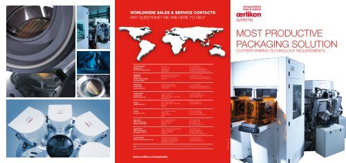
wOrLDwIDE SaLES & SErVICE CONTaCTS<br />
ANy QUESTIONS? WE ARE HERE TO HELP<br />
LIECHTENSTEIN<br />
Headquarters<br />
OC Oerlikon Balzers Ltd.<br />
GErmaNy<br />
EmEa Hub<br />
Oerlikon Deutschland<br />
Vertriebs GmbH<br />
amErICaS<br />
Central Hub<br />
Oerlikon USa Inc<br />
TaIwaN (rOC)<br />
Central Hub<br />
DKSH Taiwan Ltd.<br />
CHINa<br />
DKSH China Ltd.<br />
JapaN<br />
Hakuto Co., Ltd.<br />
maLaySIa *<br />
ZmC Technologies<br />
(malaysia) Sdn Bhd<br />
SINGapOrE *<br />
ZmC Technologies<br />
(Singapore) pte Ltd<br />
SOUTH KOrEa<br />
woowon Technology Co., Ltd<br />
Iramali 18<br />
P.O. Box 1000<br />
9496 Balzers<br />
Liechtenstein<br />
www.oerlikon.com/systems<br />
Karl-Hammerschmidt-Strasse 34<br />
85609 Aschheim-Dornach<br />
Germany<br />
10050 16th Street North<br />
St. Petersburg FL 33716<br />
United States<br />
13F-1, No.100, Sec. 1,<br />
Jiafong 11th Rd.<br />
Jhubei City, Hsinchu County 302<br />
Taiwan (R.O.C.)<br />
1801 Hongmei Road<br />
Innov Tower / Block A Unit 2208<br />
Shanghai<br />
China<br />
1-13. Shinjuku 1-Chome<br />
Shinjuku-ku<br />
Tokyo 160-8910<br />
Japan<br />
No. 1-3-23 Krystal Point 2<br />
Lebuh Bukit Kecil 6<br />
Penang 11900<br />
Malaysia<br />
10 Ubi Crescent #05-92/93/94/95<br />
Lobby E, Ubi Techpark<br />
Singapore 408564<br />
Singapore<br />
1903 Parkview Office Tower<br />
6 Jeongja-dong, Bundang-gu<br />
Seongnam-si, Kyeonggi-do<br />
463-863 South Korea<br />
T: +423 388 4770<br />
info.systems@oerlikon.com<br />
S: sales.systems@oerlikon.com<br />
CS: service.systems@oerlikon.com<br />
T: +49 89 75 505 100<br />
S: sales.systems.mn@oerlikon.com<br />
CS: service.systems.mn@oerlikon.com<br />
T: +1 727 828 0850<br />
S: sales.systems.sp@oerlikon.com<br />
CS: service.systems.sp@oerlikon.com<br />
T: +886 3 657 8788<br />
S: jason.chen@dksh.com<br />
CS: ben.lin@dksh.com<br />
T: +86 21 5383 8811<br />
S: kai.liao@dksh.com<br />
S: +81-3-3225-8992<br />
CS: +81-3-3225-8992<br />
S: HKT-oerlikon@hakuto.co.jp<br />
T: +60 4 646 4586<br />
S: yf_lau@zmc.net<br />
CS: pf_lau@zmc.net<br />
STL: julie_khoo@zmc.net<br />
T: +65 6285 1161<br />
S: steven_ho@zmc.net<br />
CS: jiang_ez@zmc.net<br />
STL: carmen_leong@zmc.net<br />
T: +82 31 783 4770<br />
S: jskim@wwtech.co.kr<br />
CS: igseo@wwtech.co.kr<br />
KEy: T: Telephone, S: Sales, CS: Customer service, STL: Support, training & logistics. *Including Indonesia / Thailand / Philippines<br />
HEX/6P/EN/08_2011<br />
<strong>MOST</strong> PRODUCTIvE<br />
<strong>PACKAGING</strong> <strong>SOLUTION</strong><br />
OUTPERFORMING TECHNOLOGy REQUIREMENTS
HEXaGON<br />
ADvANCED <strong>PACKAGING</strong> <strong>SOLUTION</strong><br />
FOR HIGH vOLUME PRODUCTION<br />
Innovation Has A Name – Cost of Ownership does too<br />
At Oerlikon, we understand the pressure you have to lower your cost per wafer. That’s why our<br />
newest tool for advanced packaging more than doubles wafer throughput, has a 50% smaller<br />
footprint than its competitors, and runs up to 5000 wafers before requiring maintenance.<br />
prODUCTIVITy<br />
Cost per wafer<br />
J J Highest Throughput<br />
JJ Smallest Footprint<br />
JJ Lowest Energy Consumption<br />
reliability<br />
J J Proven Process Components<br />
J J Proven Material Handling Systems<br />
J J Proven Control Backbone<br />
availability<br />
J J Designed for Organic Passivation Layers<br />
J J Highest Wafer Count per Maintenance Interval<br />
J J Temperature Controlled Shields and Targets<br />
maintainability<br />
J J Drop-in Shield Kits<br />
JJ Powered Source Handling<br />
J J Automated Maintenance Services<br />
FEaTUrES<br />
300mm or 200/300mm Bridge Capability<br />
process Capabilities<br />
JJ DC/DCp Sputtering<br />
JJ ICP Etching<br />
JJ Thermal Pre-Treatment<br />
JJ Ultra Low Temperature Cleaning<br />
Chucks<br />
JJ Temperature Controlled<br />
JJ Full Face, Clamped, ESC, Floating<br />
JJ RF or DC Biased<br />
Chambers<br />
JJ Full Metal Sealed Stainless Steel Process Chambers<br />
JJ Full Process Isolation<br />
JJ UHv Pumping and vacuum Capacity<br />
Transfer System<br />
JJ Up to four FOUP Atmospheric Front End<br />
JJ High Throughput Synchronous Motion Indexer<br />
JJ Wafer Position Monitoring<br />
JJ Mechanically Confined Wafer Transfers<br />
J Cryogenic Gates and Toroidal Chamber Design for<br />
Open Source Isolation<br />
Operability<br />
J Fully Pre-Integrated Systems for Fast Installation<br />
J 90% Spare Part Overlap with Previous Generation<br />
J 90% Process Matching with Previous Generation<br />
J 100% Control and Operation Compatibility with<br />
Previous Generation<br />
UNDER BUMP & RE-DISTRIBUTION METALLIzATION<br />
JJ System integration and packaging are responsible for the functionality, quality and<br />
economy of microelectronic products.<br />
JJ UBM and RDL films are commonly used in todays advanced packaging industry.<br />
The main requirements include Oxide free IC final metal pads, no damage etch step,<br />
good adhesion to the chip surface and even more importand to the chip passivation,<br />
hermetic seal to the chip passivation, good diffusion barrier between solder bump<br />
metals and IC final metal,sufficient wetability of the UBM and low stress metal stack.<br />
JJ UBM for Flip Chip, WLP and SIP production solutions eg. Ti-Cu, WTi-Cu etc.<br />
JJ Oerlikon the market leader in packaging<br />
ENHANCED WAFER LEvEL <strong>PACKAGING</strong><br />
JJ The eWLB technology allows the realization of chips with a high<br />
number of interconnects. The package is not realized on a silicon<br />
wafer as for classical Wafer Level Package, but on an artificial wafer.<br />
Therefore a front-end-processed wafer is diced and the singulated<br />
chips are placed on a carrier.<br />
JJ HEXAGON the ideal system to do eWLB production<br />
3D &THROUGH SILICON <strong>PACKAGING</strong><br />
JJ Traditional scaling of semiconductor chips also improves signal<br />
propagation speed. 3-D integrated circuits address the scaling challenge<br />
by stacking 2-D dies an connecting them in the 3rd dimension. This<br />
promises to speed up communication between layered chips. 3D<br />
ICs promise many significant benefits including: Footprint, Cost,<br />
Heterogeneous integration, Shorter interconnect, Power, Design, Circuit<br />
security<br />
J J Another application for the HEXAGON<br />
THIN WAFER & BACKSIDE METALLIzATION<br />
JJ Backside metallization on thin wafers are required to either build a<br />
solder contact for improved heat drain or create an ohmic contact<br />
layer, typically used in power device (IGBT), processors, graphic chips<br />
etc.<br />
JJ Handling reliability is one of the key advantages of the HEXAGON<br />
HEXaGON<br />
TECHNICAL INFORMATION<br />
THrOUGHpUT<br />
JJ 100 Wafers-per-hour (Wph) Handling Limit<br />
JJ Conventional UBM Processing: 56 Wph<br />
JJ Enhanced UBM Processing: 68 Wph<br />
JJ High Output UBM Processing: 80Wph<br />
FOOT prINT & LayOUT<br />
JJ 12m2 Equipment Mainframe<br />
JJ 5m2 Support and Control Systems<br />
JJ 17m2 Total Installation Area<br />
Less than half of any other<br />
commercially available System<br />
prODUCTIVITy<br />
JJ Over 90% typical availability<br />
JJ Over 4000 wafers maintenance intervals<br />
JJ Less than 6 hours Total Equipment Maintenance Time<br />
JJ Breakage rate Less than 1:20k<br />
JJ Mean Time Between Failure over 500 hours<br />
Above: The revolving carousel on HEXAGON Below: At just 12m 2 the HEXAGON mainframe