Technology of Q 2500 colour TV set
Technology of Q 2500 colour TV set Technology of Q 2500 colour TV set
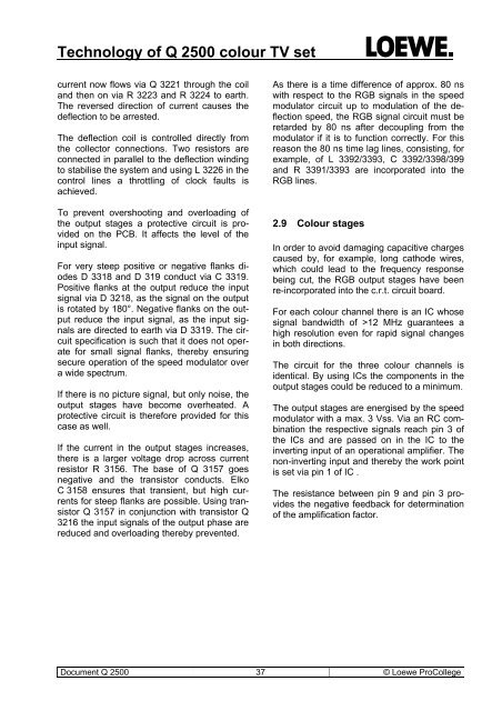
Technology of Q 2500 colour TV setW3201to signal board987654321CUTOFFU12Q2500 Speed modulatorC3182RGBQ3181R3181R3185U12Rto W548 basic boardW33015pol. ws123 Uf45L33664u7R3366270RC3172GQ3171R3171GU12C3208R3207C32103R3 SI R3153UvidC336622uC3162BR3175Q3161R3161U12BR3208Q3204Q3211R3209R3206R3215Q3157R3156C3158R3218C3221R3221R3229Q3221C3156C3157C3154C3202C3201C3203C3204R3165R3204R3212C3212R3211Q3216R3216R3220R3217C3216D3218D3219R3219C3222R3222C3219C3223R3224 R322356kR3225Q3222R3228L3226N60R3227 R3226470R 470RW3258321to booster coilSVM2.8.2 Switching of the speed modulatorThe circuit is located on the c.r.t. PCB and issupplied with RGB signals from TDA 9332 viapins 40/41/42.The RGB signals are applied to connectorW 3201 pins 4, 6, 8 at 3 Vss and are then fedvia impedance converters Q 3181, Q 3171and Q 3161. To detect changes in all threecolours, the signals are decoupled by capacitorsC 3201, C 3202 and C 3203 together.The resulting signal is differentiated withC 3204, R 3204. Control via the RGB signalsoffers the advantage that this circuit alsoworks with Teletext and OSD operation.This means that when steep signal changesoccur there are only oscillation packages withmax. 0.3 Vss on the emitter of transistorQ 3204 for processing.The input for the circuit of transistor Q 3204has a low resistance input, so that it can processsteep slopes. From the collector the 4 Vsssignals are led to the impedance converter Q3211. This supplies the signal at 6 Vss to thepush-pull output stage Q 3221 and Q 3222.The two transistors are current counter coupledand amplify the signal to a maximum 50Vss. All voltage data refers to a black/whitechange and maximum contrast.Via the voltage dividers R 3221, R 3222, R3223 and R 3224 one end of the correctioncoil on pin 1 of W 3258 is set to 30 V.The two transistors Q 3221 and Q 3222 areblocked without control, so that the other endof the coil is hanging free and no current flowsthrough the coil. Deflection occurs only via thehorizontal deflection coil.For a positive pulse transistor Q 3221 isblocked and Q 3222 conducts. This causes acurrent to flow via R 3221 and R 3222 throughthe booster coil and via Q 3222 to earth,which accelerates the deflection.If, however, a negative pulse is felt, then Q3221 conducts and Q 3222 is blocked. TheDocument Q 2500 36 © Loewe ProCollege
Technology of Q 2500 colour TV setcurrent now flows via Q 3221 through the coiland then on via R 3223 and R 3224 to earth.The reversed direction of current causes thedeflection to be arrested.The deflection coil is controlled directly fromthe collector connections. Two resistors areconnected in parallel to the deflection windingto stabilise the system and using L 3226 in thecontrol lines a throttling of clock faults isachieved.To prevent overshooting and overloading ofthe output stages a protective circuit is providedon the PCB. It affects the level of theinput signal.For very steep positive or negative flanks diodesD 3318 and D 319 conduct via C 3319.Positive flanks at the output reduce the inputsignal via D 3218, as the signal on the outputis rotated by 180°. Negative flanks on the outputreduce the input signal, as the input signalsare directed to earth via D 3319. The circuitspecification is such that it does not operatefor small signal flanks, thereby ensuringsecure operation of the speed modulator overa wide spectrum.If there is no picture signal, but only noise, theoutput stages have become overheated. Aprotective circuit is therefore provided for thiscase as well.If the current in the output stages increases,there is a larger voltage drop across currentresistor R 3156. The base of Q 3157 goesnegative and the transistor conducts. ElkoC 3158 ensures that transient, but high currentsfor steep flanks are possible. Using transistorQ 3157 in conjunction with transistor Q3216 the input signals of the output phase arereduced and overloading thereby prevented.As there is a time difference of approx. 80 nswith respect to the RGB signals in the speedmodulator circuit up to modulation of the deflectionspeed, the RGB signal circuit must beretarded by 80 ns after decoupling from themodulator if it is to function correctly. For thisreason the 80 ns time lag lines, consisting, forexample, of L 3392/3393, C 3392/3398/399and R 3391/3393 are incorporated into theRGB lines.2.9 Colour stagesIn order to avoid damaging capacitive chargescaused by, for example, long cathode wires,which could lead to the frequency responsebeing cut, the RGB output stages have beenre-incorporated into the c.r.t. circuit board.For each colour channel there is an IC whosesignal bandwidth of >12 MHz guarantees ahigh resolution even for rapid signal changesin both directions.The circuit for the three colour channels isidentical. By using ICs the components in theoutput stages could be reduced to a minimum.The output stages are energised by the speedmodulator with a max. 3 Vss. Via an RC combinationthe respective signals reach pin 3 ofthe ICs and are passed on in the IC to theinverting input of an operational amplifier. Thenon-inverting input and thereby the work pointis set via pin 1 of IC .The resistance between pin 9 and pin 3 providesthe negative feedback for determinationof the amplification factor.Document Q 2500 37 © Loewe ProCollege
- Page 1 and 2: Technology of Q 2500 colour TV set2
- Page 3 and 4: Technology of Q 2500 colour TV set1
- Page 5 and 6: Technology of Q 2500 colour TV set1
- Page 7 and 8: Technology of Q 2500 colour TV set1
- Page 9 and 10: Technology of Q 2500 colour TV setF
- Page 11 and 12: Technology of Q 2500 colour TV setS
- Page 13 and 14: Technology of Q 2500 colour TV setQ
- Page 15 and 16: Technology of Q 2500 colour TV setQ
- Page 17 and 18: Technology of Q 2500 colour TV setW
- Page 19 and 20: Technology of Q 2500 colour TV setQ
- Page 21 and 22: Technology of Q 2500 colour TV set2
- Page 23 and 24: Technology of Q 2500 colour TV setD
- Page 25 and 26: Technology of Q 2500 colour TV set2
- Page 27 and 28: Technology of Q 2500 colour TV setC
- Page 29 and 30: Technology of Q 2500 colour TV setW
- Page 31 and 32: Technology of Q 2500 colour TV setV
- Page 33 and 34: Technology of Q 2500 colour TV setT
- Page 35: Technology of Q 2500 colour TV setJ
- Page 39 and 40: Technology of Q 2500 colour TV setL
- Page 41 and 42: Technology of Q 2500 colour TV setT
- Page 43 and 44: Technology of Q 2500 colour TV setO
- Page 45 and 46: Technology of Q 2500 colour TV setI
- Page 47 and 48: Technology of Q 2500 colour TV setc
- Page 49 and 50: Technology of Q 2500 colour TV setF
- Page 51 and 52: Technology of Q 2500 colour TV setF
- Page 53 and 54: Technology of Q 2500 colour TV sett
- Page 55 and 56: Technology of Q 2500 colour TV setS
- Page 57 and 58: Technology of Q 2500 colour TV setP
- Page 59 and 60: Technology of Q 2500 colour TV set3
- Page 61 and 62: Technology of Q 2500 colour TV setB
- Page 63 and 64: Technology of Q 2500 colour TV setr
- Page 65 and 66: Technology of Q 2500 colour TV setA
- Page 67 and 68: Technology of Q 2500 colour TV set-
- Page 70 and 71: Technology of Q 2500 colour TV setT
- Page 72 and 73: Technology of Q 2500 colour TV setI
- Page 74 and 75: Technology of Q 2500 colour TV setT
- Page 76 and 77: Technology of Q 2500 colour TV set4
- Page 78 and 79: Technology of Q 2500 colour TV setC
- Page 80 and 81: Technology of Q 2500 colour TV set4
- Page 82 and 83: Technology of Q 2500 colour TV setQ
- Page 84 and 85: Technology of Q 2500 colour TV setH
<strong>Technology</strong> <strong>of</strong> Q <strong>2500</strong> <strong>colour</strong> <strong>TV</strong> <strong>set</strong>current now flows via Q 3221 through the coiland then on via R 3223 and R 3224 to earth.The reversed direction <strong>of</strong> current causes thedeflection to be arrested.The deflection coil is controlled directly fromthe collector connections. Two resistors areconnected in parallel to the deflection windingto stabilise the system and using L 3226 in thecontrol lines a throttling <strong>of</strong> clock faults isachieved.To prevent overshooting and overloading <strong>of</strong>the output stages a protective circuit is providedon the PCB. It affects the level <strong>of</strong> theinput signal.For very steep positive or negative flanks diodesD 3318 and D 319 conduct via C 3319.Positive flanks at the output reduce the inputsignal via D 3218, as the signal on the outputis rotated by 180°. Negative flanks on the outputreduce the input signal, as the input signalsare directed to earth via D 3319. The circuitspecification is such that it does not operatefor small signal flanks, thereby ensuringsecure operation <strong>of</strong> the speed modulator overa wide spectrum.If there is no picture signal, but only noise, theoutput stages have become overheated. Aprotective circuit is therefore provided for thiscase as well.If the current in the output stages increases,there is a larger voltage drop across currentresistor R 3156. The base <strong>of</strong> Q 3157 goesnegative and the transistor conducts. ElkoC 3158 ensures that transient, but high currentsfor steep flanks are possible. Using transistorQ 3157 in conjunction with transistor Q3216 the input signals <strong>of</strong> the output phase arereduced and overloading thereby prevented.As there is a time difference <strong>of</strong> approx. 80 nswith respect to the RGB signals in the speedmodulator circuit up to modulation <strong>of</strong> the deflectionspeed, the RGB signal circuit must beretarded by 80 ns after decoupling from themodulator if it is to function correctly. For thisreason the 80 ns time lag lines, consisting, forexample, <strong>of</strong> L 3392/3393, C 3392/3398/399and R 3391/3393 are incorporated into theRGB lines.2.9 Colour stagesIn order to avoid damaging capacitive chargescaused by, for example, long cathode wires,which could lead to the frequency responsebeing cut, the RGB output stages have beenre-incorporated into the c.r.t. circuit board.For each <strong>colour</strong> channel there is an IC whosesignal bandwidth <strong>of</strong> >12 MHz guarantees ahigh resolution even for rapid signal changesin both directions.The circuit for the three <strong>colour</strong> channels isidentical. By using ICs the components in theoutput stages could be reduced to a minimum.The output stages are energised by the speedmodulator with a max. 3 Vss. Via an RC combinationthe respective signals reach pin 3 <strong>of</strong>the ICs and are passed on in the IC to theinverting input <strong>of</strong> an operational amplifier. Thenon-inverting input and thereby the work pointis <strong>set</strong> via pin 1 <strong>of</strong> IC .The resistance between pin 9 and pin 3 providesthe negative feedback for determination<strong>of</strong> the amplification factor.Document Q <strong>2500</strong> 37 © Loewe ProCollege


