Technology of Q 2500 colour TV set
Technology of Q 2500 colour TV set
Technology of Q 2500 colour TV set

Create successful ePaper yourself
Turn your PDF publications into a flip-book with our unique Google optimized e-Paper software.
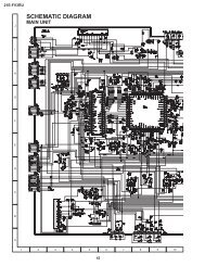
<strong>Technology</strong> <strong>of</strong> Q <strong>2500</strong> <strong>colour</strong> <strong>TV</strong> <strong>set</strong>C541C5432.5.1 CircuitThe components <strong>of</strong> the east/west outputstage, as well as the diode modulator are locatedon the basic board.W511Pin1VPROTR598C596R596Q597Q596R597Hor.vom Signal-BoardHorizontaldeflectorE/WchargingcoilC590Q534C581R581R582Q582C582R583Q589D584D539aD539bQ534C541R585D539aD539bUBE/W correctionR587C589R584L543C531C543R588Q593R589L539L588C588Q59312 3L541L536U12R593R592R591SplittingtransformerT531R590L590D590D589The video/deflection processor TDA 9332 appliesa d.c. underlying parabola type voltageto pin 3. This Information contains all correctionsfor picture width and east/west. The followingamplifier stage, consisting <strong>of</strong> transistorsQ 582 to Q 589, could therefore be implementedsimply as a conventionally baseddifferential amplifier.Control is via low-pass filter R 581, C 581 andR 582 on the base <strong>of</strong> transistor Q 582. Thelow-pass filter suppresses any noise componentsfrom the pulse width generator inI 2521.The base <strong>of</strong> transistor Q 589 is determined bythe voltage divider R 588/R 589 in d.c. andthereby determines the operational point <strong>of</strong>the differential amplifier.The amplification <strong>of</strong> the differential amplifier isdetermined essentially by the relationship <strong>of</strong>the negative feedback resistance R 583 andthe output resistances R 581/582. The parabolatype voltage, amplified to 12 V by outputstages Q 585 and Q 586, is fed via the E/Wcharge coil to the diode modulator. Dual diodeD 539 superimposes the deflection current onit and the E/W correction is implemented.Transistor Q 593 was incorporated to protectthe output stage transistor Q 586 in the event<strong>of</strong> the deflection connector being withdrawn.Normally Q 593 acts as positive feedback toQ 586. If the deflection connector is withdrawnthe current increases through Q 586 andtherefore also through resistors R 591 /R 592.This causes Q 593 to conduct and the powerloss in Q 586 to be returned to a normal level.In the event <strong>of</strong> a fault the two transistorsQ 596 and Q 597 ensure that the unitswitches to protective operation. Q 596 isconductively controlled by a reduced basevoltage. Q 597 conducts and controls VPROTat low level. The CCU protective circuit respondsand switches the unit <strong>of</strong>f.R586Q586C590Document Q <strong>2500</strong> 27 © Loewe ProCollege