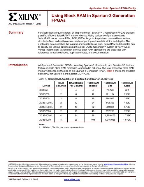
Xilinx XAPP463 Using Block RAM in Spartan-3 Generation FPGAs ...
Xilinx XAPP463 Using Block RAM in Spartan-3 Generation FPGAs ...
Xilinx XAPP463 Using Block RAM in Spartan-3 Generation FPGAs ...
Create successful ePaper yourself
Turn your PDF publications into a flip-book with our unique Google optimized e-Paper software.
<strong>Us<strong>in</strong>g</strong> <strong>Block</strong> <strong>RAM</strong> <strong>in</strong> <strong>Spartan</strong>-3 <strong>Generation</strong> <strong>FPGAs</strong>RTable 5: <strong>Block</strong> <strong>RAM</strong> Attributes and VHDL/Verilog Attribute Names (Cont<strong>in</strong>ued)Function VHDL or Verilog Attribute Default ValueData Output Latch SynchronousSet/Reset ValueNumber of PortsSRVAL (s<strong>in</strong>gle-port)SRVAL_A, SRVAL_B (dual-port)Reset to zeroData Output Latch Behavior dur<strong>in</strong>g WRITE_MODEWRITE_FIRSTWrite<strong>Block</strong> <strong>RAM</strong> Location LOC N/AAlthough physically dual-port memory, each block <strong>RAM</strong> performs as either s<strong>in</strong>gle-port or dualportmemory. The method to specify the number of ports depends on the design entry tool.CORE Generator SystemAs shown <strong>in</strong> Figure 5, the <strong>Xil<strong>in</strong>x</strong> CORE Generator system provides module generators forvarious types of memory blocks. Choose s<strong>in</strong>gle- or dual-port block memories, or use thehigher-level functions to create FIFOs, content-addressable memories (CAMs), and so forth.Figure 5: Select<strong>in</strong>g a <strong>Block</strong> <strong>RAM</strong> Function <strong>in</strong> CORE Generator SystemVHDL or Verilog InstantiationThe <strong>Xil<strong>in</strong>x</strong> design libraries conta<strong>in</strong> s<strong>in</strong>gle- and dual-port memory primitives similar to thoseshown <strong>in</strong> Figure 1. Select among the various primitives to choose s<strong>in</strong>gle- or dual-port memory,as well as the memory organization or aspect ratio of the memory. See Table 6 and Table 7 fors<strong>in</strong>gle-port and dual-port block <strong>RAM</strong> primitives, respectively.Memory Organization/Aspect RatioThe data organization or aspect ratio of a <strong>RAM</strong> block is configurable, as shown <strong>in</strong> Table 6. If thedata path is byte-wide or wider, then the block <strong>RAM</strong> also provides additional bits to supportparity for each byte. Consequently, a 1Kx18 memory organization is 18 bits wide with 16 bits(two bytes) allocated to data plus two parity bits, one for each byte. Also, the physical amountof memory accessible from a port depends on the memory organization. For memories bytewideand wider, there are 18K memory bits accessible. For narrower memories, only 16K bitsare accessible due to the lack of parity bits <strong>in</strong> these organizations. Essentially, 16K bits areallocated to data, 2K bits to parity on the 18K-bit block <strong>RAM</strong>. See Figure 4 for details on datamapp<strong>in</strong>g for and between each memory organization.<strong>XAPP463</strong> (v2.0) March 1, 2005 www.xil<strong>in</strong>x.com 9
R<strong>Us<strong>in</strong>g</strong> <strong>Block</strong> <strong>RAM</strong> <strong>in</strong> <strong>Spartan</strong>-3 <strong>Generation</strong> <strong>FPGAs</strong>Table 6: <strong>Block</strong> <strong>RAM</strong> Data Organizations/Aspect RatiosOrganizationMemoryDepthDataWidthParityWidth DI/DO DIP/DOP ADDRS<strong>in</strong>gle-PortPrimitiveTotal <strong>RAM</strong>Kbits512x36 512 32 4 (31:0) (3:0) (8:0) <strong>RAM</strong>B16_S36 18K1Kx18 1024 16 2 (15:0) (1:0) (9:0) <strong>RAM</strong>B16_S18 18K2Kx9 2048 8 1 (7:0) (0:0) (10:0) <strong>RAM</strong>B16_S9 18K4Kx4 4096 4 - (3:0) - (11:0) <strong>RAM</strong>B16_S4 16K8Kx2 8192 2 - (1:0) - (12:0) <strong>RAM</strong>B16_S2 16K16Kx1 16384 1 - (0:0) - (13:0) <strong>RAM</strong>B16_S1 16KCORE Generator System — Memory SizeThe CORE Generator system creates a wide variety of memories with very flexible aspectratios. Unlike the actual block <strong>RAM</strong> primitive, the CORE generator system does not differentiatebetween data and parity bits and considers all bits data bits. For dual-port memories, each portcan have different organizations or aspect ratios.With<strong>in</strong> the CORE Generator system, locate the Memory Size group and enter the desiredmemory organization, as shown <strong>in</strong> Figure 6.Memory SizeWidth 16Valid Range 1..256Depth 256Valid Range 2..16384Figure 6: Select<strong>in</strong>g Memory Width and Depth <strong>in</strong> CORE Generator SystemVHDL or Verilog InstantiationThe aspect ratio is def<strong>in</strong>ed at design time by specify<strong>in</strong>g or <strong>in</strong>stantiat<strong>in</strong>g the appropriateSelect<strong>RAM</strong> component. Table 6 <strong>in</strong>dicates the Select<strong>RAM</strong> component for s<strong>in</strong>gle-port <strong>RAM</strong>. Fors<strong>in</strong>gle-port <strong>RAM</strong>, the proper component name is <strong>RAM</strong>B16_Sn, where n is the data path width<strong>in</strong>clud<strong>in</strong>g both the data bits plus parity bits. For example, a 1Kx18 s<strong>in</strong>gle-port <strong>RAM</strong> usescomponent <strong>RAM</strong>B16_S18. In this example, n=18 because there are 16 data bits plus 2 paritybits.Select<strong>in</strong>g a dual-port memory is slightly more complex because the two memory ports mayhave different aspect ratios. For dual-port <strong>RAM</strong>, the proper component name is<strong>RAM</strong>B16_Sm_Sm, where m is the data path width for Port A and n is the width for Port B. Forexample, us<strong>in</strong>g the suffix shown <strong>in</strong> Table 7, if Port A is organized a 2Kx9 and Port B isorganized as 1Kx18, then the proper dual-port <strong>RAM</strong> component is <strong>RAM</strong>B16_S9_S18. In thisexample, m=9 and n=18.Table 7: Dual-Port <strong>RAM</strong> Component Suffix Appended to “<strong>RAM</strong>B16”Port A16Kx1 8Kx2 4Kx4 2Kx9 1Kx18 512x3616Kx1 _S1_S18Kx2 _S1_S2 _S2_S24Kx4 _S1_S4 _S2_S4 _S4_S42Kx9 _S1_S9 _S2_S9 _S4_S9 _S9_S91Kx18 _S1_S18 _S2_S18 _S4_S18 _S9_S18 _S18_S18512x36 _S1_S36 _S2_S36 _S4_S36 _S9_S36 _S18_S36 _S36_S36Port B10 www.xil<strong>in</strong>x.com <strong>XAPP463</strong> (v2.0) March 1, 2005
<strong>Us<strong>in</strong>g</strong> <strong>Block</strong> <strong>RAM</strong> <strong>in</strong> <strong>Spartan</strong>-3 <strong>Generation</strong> <strong>FPGAs</strong>RAddress and Data Mapp<strong>in</strong>g Between Two PortsIn dual-port mode, both ports access the same set of memory cells. However, both ports mayhave the same or different memory organization or aspect ratio. Figure 4 shows how the samedata set may appear with different aspect ratios.There are extra bits available to store parity for memory organizations that are byte-wide orwider. The extra parity bits are designed to be associated with a particular byte and these paritybits appear as the more-significant bits on the data port. For example, if a x36 data word (32data, 4 parity) is addressed as two x18 halfwords (16 data, 2 parity), the parity bits associatedwith each data byte are mapped with<strong>in</strong> the block <strong>RAM</strong> to appropriate parity bits. The sameeffect happens when the x36 data word is mapped as four x9 words. The extra parity bits arenot available if the data port is configured as x4, x2, or x1.The follow<strong>in</strong>g formulas provide the start<strong>in</strong>g and end<strong>in</strong>g address for data when the two portshave different memory organizations. F<strong>in</strong>d the start<strong>in</strong>g and end<strong>in</strong>g address for Port X given theaddress and port width of Port Y and the port width of Port X.START_ADDRESS X=INTEGERADDRESS YWIDTH⎛•------------------------------------------------- Y ⎞⎝⎠WIDTH XEND_ADDRESS X=INTEGER( ADDRESS Y+ 1) WIDTH⎛( • Y) – 1-----------------------------------------------------------------------------⎞⎝⎠WIDTH XIf, due the memory organization, one port <strong>in</strong>cludes parity bits and the other does not, then theabove equations are <strong>in</strong>valid and the values for width should only <strong>in</strong>clude the data bits. Theparity bits are not available on any port that is less than 8 bits wide.Content InitializationBy default, block <strong>RAM</strong> memory is <strong>in</strong>itialized with all zeros dur<strong>in</strong>g the device configurationsequence. However, the contents can also be <strong>in</strong>itialized with user-def<strong>in</strong>ed data. Furthermore,the <strong>RAM</strong> contents are protected aga<strong>in</strong>st spurious writes dur<strong>in</strong>g configuration.CORE Generator System — Load Init FileTo specify the <strong>in</strong>itial <strong>RAM</strong> contents for a CORE Generator block <strong>RAM</strong> function, create acoefficients (.coe) file. A simple example of a coefficients file appears <strong>in</strong> Figure 7. At am<strong>in</strong>imum, def<strong>in</strong>e the radix for the <strong>in</strong>itialization data—i.e., base 2, 10, or 16—and then specifythe <strong>RAM</strong> contents start<strong>in</strong>g with the data at location 0, followed by data at subsequent locations.memory_<strong>in</strong>itialization_radix=16;memory_<strong>in</strong>itialization_vector= 80, 0F, 00, 0B, 00, 0C, …, 81;Figure 7: A Simple Coefficients File (.coe) ExampleTo <strong>in</strong>clude the coefficients file, locate the appropriate section <strong>in</strong> the CORE Generator wizardand check Load Init File, as shown <strong>in</strong> Figure 8. Then, click Load File and select thecoefficients file.Initial ContentsGlobal Init Value:ff0001(Hex Value)Load Init FileLoad File ...C:\MyProject\my_ram_<strong>in</strong>it.coe(.coe File)Figure 8: Specify<strong>in</strong>g Initial <strong>RAM</strong> Contents <strong>in</strong> CORE Generator System<strong>XAPP463</strong> (v2.0) March 1, 2005 www.xil<strong>in</strong>x.com 11
R<strong>Us<strong>in</strong>g</strong> <strong>Block</strong> <strong>RAM</strong> <strong>in</strong> <strong>Spartan</strong>-3 <strong>Generation</strong> <strong>FPGAs</strong>VHDL or Verilog Instantiation — INIT_xx, INITP_xxFor VHDL and Verilog <strong>in</strong>stantiation, there are two different types of <strong>in</strong>itialization attributes. TheINIT_xx attributes def<strong>in</strong>e the <strong>in</strong>itial contents of the data memory locations. The INITP_xxattributes def<strong>in</strong>e the <strong>in</strong>itial contents of the parity memory locations.The INIT_xx attributes on the <strong>in</strong>stantiated primitive def<strong>in</strong>e the <strong>in</strong>itial memory contents. Thereare 64 <strong>in</strong>itialization attributes, named INIT_00 through INIT_3F. Each INIT_xx attribute is a64-digit (256-bit) hex-encoded bit vector. The memory contents can be partially <strong>in</strong>itialized andany unspecified locations are automatically completed with zeros.The follow<strong>in</strong>g formula def<strong>in</strong>es the bit positions for each INIT_xx attribute.Given yy = convert_hex_to_decimal(xx), INIT_xx corresponds to the follow<strong>in</strong>g memory cells.• Start<strong>in</strong>g Location: [(yy + 1) * 256] –1• End Location: (yy) * 256For example, for the attribute INIT_1F, the conversion is as follows:• yy = convert_hex_to_decimal(0x1F) = 31• Start<strong>in</strong>g Location: [(31+1) * 256] –1 = 8191• End Location: 31 * 256 = 7936Table 8: VHDL/Verilog <strong>RAM</strong> Initialization Attributes for <strong>Block</strong> <strong>RAM</strong>Attribute From ToINIT_00 255 0INIT_01 511 256INIT_02 767 512… … …INIT_3F 16383 16128The INITP_xx attributes def<strong>in</strong>e the <strong>in</strong>itial contents of the memory cells correspond<strong>in</strong>g to paritybits, i.e., those bits that connect to the DIP/DOP buses. By default these memory cells are also<strong>in</strong>itialized to all zeros.The eight <strong>in</strong>itialization attributes from INITP_00 through INITP_07 represent the memorycontents of parity bits. Each INITP_xx is a 64-digit (256-bit) hex-encoded bit vector andbehaves like an INIT_xx attribute. The same formula calculates the bit positions <strong>in</strong>itialized bya particular INITP_xx attribute.Data Output Latch InitializationThe block <strong>RAM</strong> output latches can be <strong>in</strong>itialized to a user-specified value immediately afterconfiguration or whenever the global set/reset signal, GSR, is asserted. For dual-portmemories, there is a separate <strong>in</strong>itialization value for each port.If no value is specified, the output latch is <strong>in</strong>itialized to zero.12 www.xil<strong>in</strong>x.com <strong>XAPP463</strong> (v2.0) March 1, 2005
<strong>Us<strong>in</strong>g</strong> <strong>Block</strong> <strong>RAM</strong> <strong>in</strong> <strong>Spartan</strong>-3 <strong>Generation</strong> <strong>FPGAs</strong>RCORE Generator System — Global Init ValueFigure 9 describes how to specify the <strong>in</strong>itial value for data output latches <strong>in</strong> the COREGenerator system. The value, specified <strong>in</strong> hexadecimal, should <strong>in</strong>clude one bit per the specifieddata width. For dual-port memories, there is a separate <strong>in</strong>itialization value for each port.Initial ContentsGlobal Init Value:ff0001(Hex Value)Load Init FileLoad File ...C:\MyProject\my_ram_<strong>in</strong>it.coe(.coe File)Figure 9: Specify<strong>in</strong>g Initial Value for <strong>Block</strong> <strong>RAM</strong> Data Output LatchesVHDL or Verilog Instantiation — INIT (INIT_A and INIT_B)For VHDL or Verilog, the INIT attribute (or INIT_A and INIT_B for dual-port memories) def<strong>in</strong>esthe output latch value after configuration. The INIT (or INIT_A and INIT_B) attribute specifiesthe <strong>in</strong>itial value for the data and, if applicable, the parity bits. Figure 4 shows the expected bitformat for each memory organization with parity bits—if applicable—as the more significant bitsfollowed by the data bits. For example, the <strong>in</strong>itialization value for a 2Kx9 memory would ben<strong>in</strong>e bits wide and would <strong>in</strong>clude one parity bit followed by eight data bits. These attributes arehex-encoded bit vectors and the default value is 0.Data Output Latch Synchronous Set/Reset ValueWhen the synchronous set/reset <strong>in</strong>put, SSR, is asserted, the data output latches are set orreset accord<strong>in</strong>g to the set/reset value attribute. For dual-port memories, there is a separate<strong>in</strong>itialization value for each port.If no value is specified, the output latch is reset to zero dur<strong>in</strong>g a valid Synchronous Set/Resetoperation.CORE Generator System — Init Value (SINIT)Figure 10 describes how to specify the synchronous set/reset value for data output latches <strong>in</strong>the CORE Generator system. Check the SINIT p<strong>in</strong> and then specify the synchronous set/resetvalue <strong>in</strong> hexadecimal, with one bit per the specified data width. For dual-port memories, thereis a separate value for each port.Output Register OptionsAdditional Output Pipe Stages0SINIT p<strong>in</strong> (sync. reset of output registers)Init Value (Hex)a5a50fFigure 10: Specify<strong>in</strong>g the Output Data Latch Set/Reset ValueVHDL or Verilog Instantiation — SRVAL (SRVAL_A and SRVAL_B)For VHDL or Verilog, the SRVAL attribute (or SRVAL_A and SRVAL_B for dual-port memories)def<strong>in</strong>es the output latch value after configuration. The SRVAL (or SRVAL_A and SRVAL_B)attribute specifies the <strong>in</strong>itial value for the data and, if applicable, the parity bits. Figure 4 showsthe expected bit format for each memory organization with parity bits—if applicable—as themore significant bits followed by the data bits. These attributes are hex-encoded bit vectorsand the default value is 0.<strong>XAPP463</strong> (v2.0) March 1, 2005 www.xil<strong>in</strong>x.com 13
R<strong>Us<strong>in</strong>g</strong> <strong>Block</strong> <strong>RAM</strong> <strong>in</strong> <strong>Spartan</strong>-3 <strong>Generation</strong> <strong>FPGAs</strong>Read Behavior Dur<strong>in</strong>g Simultaneous Write — WRITE_MODETo maximize data throughput and utilization of the dual-port memory at each clock edge, block<strong>RAM</strong> memory supports one of three write modes for each memory port. These different modesdeterm<strong>in</strong>e which data is available on the output latches after a valid write clock edge to thesame port. The default mode, WRITE_FIRST, provides backwards compatibility with the olderVirtex/Virtex-E and <strong>Spartan</strong>-IIE FPGA architectures and is also the default behavior forVirtex-II/Virtex-II Pro devices. However, READ_FIRST mode is the most useful as it<strong>in</strong>creases the efficiency of block <strong>RAM</strong> memory at each clock cycle, allow<strong>in</strong>g designs to usemaximum bandwidth. In READ_FIRST mode, a memory port supports simultaneous read andwrite operations to the same address on the same clock edge, free of any tim<strong>in</strong>g complications.Table 9 outl<strong>in</strong>es how the WRITE_MODE sett<strong>in</strong>g affects the output data latches on the sameport, and how it affects the output latches on the opposite port dur<strong>in</strong>g a simultaneous access tothe same address.Table 9: WRITE_MODE Affects Data Output Latches Dur<strong>in</strong>g Write OperationsWrite ModeWRITE_FIRSTRead After Write(Default)READ_FIRSTRead Before Write(Recommended)NO_CHANGENo Read on WriteEffect on Same PortData on DI, DIP <strong>in</strong>puts written <strong>in</strong>to specified<strong>RAM</strong> location and simultaneously appears onDO, DOP outputs.Data from specified <strong>RAM</strong> location appears onDO, DOP outputs.Data on DI, DIP <strong>in</strong>puts written <strong>in</strong>to specifiedlocation.Data on DO, DOP outputs rema<strong>in</strong>s unchanged.Data on DI, DIP <strong>in</strong>puts written <strong>in</strong>to specifiedlocation.Effect on Opposite Port(dual-port mode only, same address)Invalidates data on DO, DOP outputs.Data from specified <strong>RAM</strong> location appears onDO, DOP outputs.Invalidates data on DO, DOP outputs.Mode selection is set by configuration. One of these three modes is set <strong>in</strong>dividually for eachport by an attribute. The default mode is WRITE_FIRST.WRITE_FIRST or Transparent Mode (Default)The WRITE_FIRST mode is the default operat<strong>in</strong>g mode for backward compatibility reasons.For new designs, READ_FIRST mode is recommended.In this mode, the <strong>in</strong>put data is written <strong>in</strong>to the addressed <strong>RAM</strong> location memory andsimultaneously stored <strong>in</strong> the data output latches, result<strong>in</strong>g <strong>in</strong> a transparent write operation, asshown <strong>in</strong> Figure 11. The WRITE_FIRST mode provides backwards compatibility with the 4K-bitblocks <strong>RAM</strong>s on Virtex/Virtex-E and <strong>Spartan</strong>-II/<strong>Spartan</strong>-IIE <strong>FPGAs</strong> and is also the defaultmode for Virtex-II/Virtex-II Pro block <strong>RAM</strong>s.Data_<strong>in</strong>WEENCLKAddress<strong>RAM</strong> LocationData_outWRITE_MODE = WRITE_FIRSTX463_11_062503Figure 11: Data Flow dur<strong>in</strong>g a WRITE_FIRST Write Operation14 www.xil<strong>in</strong>x.com <strong>XAPP463</strong> (v2.0) March 1, 2005
<strong>Us<strong>in</strong>g</strong> <strong>Block</strong> <strong>RAM</strong> <strong>in</strong> <strong>Spartan</strong>-3 <strong>Generation</strong> <strong>FPGAs</strong>RFigure 12 demonstrates that a valid write operation dur<strong>in</strong>g a valid read operation results <strong>in</strong> thewrite data appear<strong>in</strong>g on the data output.CLKWEData_<strong>in</strong>XXXX 1111 2222 XXXXAddressaa bb cc ddData_out0000 MEM(aa) 1111 2222 MEM(dd)ENABLEDISABLEDREADWRITEMEM(bb)=1111WRITEMEM(cc)=2222READFigure 12: WRITE_FIRST Mode WaveformsX463_12_020503READ_FIRST or Read-Before-Write ModeIn READ_FIRST mode, data previously stored at the write address appears on the outputlatches, while the new <strong>in</strong>put data is stored <strong>in</strong> memory, result<strong>in</strong>g <strong>in</strong> a read-before-write operationshown <strong>in</strong> Figure 13. The older <strong>RAM</strong> data appears on the data output while the new <strong>RAM</strong> datais stored <strong>in</strong> the specified <strong>RAM</strong> location. READ_FIRST mode is the recommended operat<strong>in</strong>gmode.Data_<strong>in</strong>WEENCLKAddress<strong>RAM</strong> LocationData_outWRITE_MODE = READ_FIRSTX463_13_062503Figure 13: Data Flow dur<strong>in</strong>g a READ_FIRST Write Operation<strong>XAPP463</strong> (v2.0) March 1, 2005 www.xil<strong>in</strong>x.com 15
R<strong>Us<strong>in</strong>g</strong> <strong>Block</strong> <strong>RAM</strong> <strong>in</strong> <strong>Spartan</strong>-3 <strong>Generation</strong> <strong>FPGAs</strong>Figure 14 demonstrates that the older <strong>RAM</strong> data always appears on the data output, regardlessof a simultaneous write operation.CLKWEData_<strong>in</strong>XXXX 1111 2222 XXXXAddressaa bb cc ddData_out0000 MEM(aa) old MEM(bb) old MEM(cc) MEM(dd)ENABLEDISABLEDREADWRITEMEM(bb)=1111WRITEMEM(cc)=2222READFigure 14: READ_FIRST Mode WaveformsX463_14_020503This mode is particularly useful for build<strong>in</strong>g circular buffers and large, block-<strong>RAM</strong>-based shiftregisters. Similarly, this mode is useful when stor<strong>in</strong>g FIR filter taps <strong>in</strong> digital signal process<strong>in</strong>gapplications. Old data is copied out from <strong>RAM</strong> while new data is written <strong>in</strong>to <strong>RAM</strong>.NO_CHANGE ModeIn NO_CHANGE mode, the output latches are disabled and rema<strong>in</strong> unchanged dur<strong>in</strong>g asimultaneous write operation, as shown <strong>in</strong> Figure 15. This behavior mimics that of simplesynchronous memory where a memory location is either read or written dur<strong>in</strong>g a clock cycle,but not both.Data_<strong>in</strong>WEENCLKAddress<strong>RAM</strong> LocationData_outWRITE_MODE = NO_CHANGEX463_15_062503Figure 15: Data Flow dur<strong>in</strong>g a NO_CHANGE Write OperationThe NO_CHANGE mode is useful <strong>in</strong> a variety of applications, <strong>in</strong>clud<strong>in</strong>g those where the block<strong>RAM</strong> conta<strong>in</strong>s waveforms, function tables, coefficients, and so forth. The memory can beupdated without affect<strong>in</strong>g the memory output.16 www.xil<strong>in</strong>x.com <strong>XAPP463</strong> (v2.0) March 1, 2005
<strong>Us<strong>in</strong>g</strong> <strong>Block</strong> <strong>RAM</strong> <strong>in</strong> <strong>Spartan</strong>-3 <strong>Generation</strong> <strong>FPGAs</strong>RFigure 16 shows that the data output reta<strong>in</strong>s the last read data if there is a simultaneous writeoperation on the same port.CLKWEData_<strong>in</strong>XXXX 1111 2222 XXXXAddressaa bb cc ddData_out0000 MEM(aa) MEM(dd)ENABLEDISABLEDREADWRITEMEM(bb)=1111WRITEMEM(cc)=2222READFigure 16: NO_CHANGE Mode WaveformsX463_16_020503CORE Generator System — Write ModeTo specify the WRITE_MODE <strong>in</strong> the CORE Generator system, locate the sett<strong>in</strong>gs for WriteMode as shown <strong>in</strong> Figure 17. Select between Read After Write (WRITE_FIRST), Read BeforeWrite (READ_FIRST) or No Read On Write (NO_CHANGE).Write ModeRead After Write Read Before Write No Read On WriteFigure 17: Select<strong>in</strong>g the Write Mode <strong>in</strong> CORE Generator SystemVHDL or Verilog Instantiation — WRITE_MODEWhen <strong>in</strong>stantiat<strong>in</strong>g block <strong>RAM</strong>, specify the write mode via the WRITE_MODE attribute.Acceptable values <strong>in</strong>clude WRITE_FIRST, READ_FIRST, and NO_CHANGE, as demonstrated<strong>in</strong> the examples <strong>in</strong> the appendices.Location Constra<strong>in</strong>ts (LOC)In general, it is best to allow the <strong>Xil<strong>in</strong>x</strong> ISE software to assign a block <strong>RAM</strong> location. However,block <strong>RAM</strong>s can be constra<strong>in</strong>ed to specific locations on a <strong>Spartan</strong>-3 device us<strong>in</strong>g an attachedLOC property. <strong>Block</strong> <strong>RAM</strong> placement locations are device specific and differ from theconvention used for nam<strong>in</strong>g CLB locations, allow<strong>in</strong>g LOC properties to transfer easily fromarray to array.The LOC properties use the follow<strong>in</strong>g form:LOC = <strong>RAM</strong>B16_X#Y#The <strong>RAM</strong>B16_X0Y0 is the lower-left block <strong>RAM</strong> location on the device, as shown <strong>in</strong> Figure 18.The upper-right block <strong>RAM</strong> location depends on n, the number of block <strong>RAM</strong> columns, and m,the number of block <strong>RAM</strong> rows, as provided <strong>in</strong> Table 1.<strong>XAPP463</strong> (v2.0) March 1, 2005 www.xil<strong>in</strong>x.com 17
R<strong>Us<strong>in</strong>g</strong> <strong>Block</strong> <strong>RAM</strong> <strong>in</strong> <strong>Spartan</strong>-3 <strong>Generation</strong> <strong>FPGAs</strong><strong>RAM</strong>B16_X0Y(m-1)UpperLeftUpperRight<strong>RAM</strong>B16_X(n-1)Y(m-1)XC3S50XC3S100En = total columnsm = total rows<strong>RAM</strong>B16_X0Y0LowerLeftLowerRightXC3S200XC3S400XC3S1000/LXC3S1500/LXC3S2000XC3S250EXC3S500EXC3S1200EXC3S1600EXC3S4000/LXC3S5000<strong>RAM</strong>B16_X(n-1)Y(m-1)Figure 18: <strong>Block</strong> <strong>RAM</strong> LOC Coord<strong>in</strong>atesX463_18_010205Location attributes cannot be specified directly <strong>in</strong> the CORE Generator system. However,location constra<strong>in</strong>ts can be added to VHDL or Verilog <strong>in</strong>stantiations.<strong>Block</strong> <strong>RAM</strong>OperationTable 10 describes the behavior of block <strong>RAM</strong> and assumes that all control signals use theirdefault, active-High behavior. However, the control signals can be <strong>in</strong>verted <strong>in</strong> the design ifnecessary. The table and follow<strong>in</strong>g text describes the behavior for a s<strong>in</strong>gle memory port. Indual-port mode, both ports perform as <strong>in</strong>dependent s<strong>in</strong>gle-port memories.All read and write operations to block <strong>RAM</strong> are synchronous. All <strong>in</strong>puts have a set-up timerelative to clock and all outputs have a clock-to-output time.Table 10: <strong>Block</strong> <strong>RAM</strong> Function TableInput Signals Output Signals <strong>RAM</strong> ContentsGSR EN SSR WE CLK ADDR DIP DI DOP DO Parity DataImmediately After ConfigurationLoaded Dur<strong>in</strong>g Configuration X X INITP_xx 2 INIT_xx 2Global Set/Reset Immediately after Configuration1 X X X X X X X INIT 3 INIT No Chg No Chg<strong>RAM</strong> Disabled0 0 X X X X X X No Chg No Chg No Chg No ChgSynchronous Set/Reset0 1 1 0 X X X SRVAL 4 SRVAL No Chg No ChgSynchronous Set/Reset dur<strong>in</strong>g Write <strong>RAM</strong>0 1 1 1 addr pdata Data SRVAL SRVAL <strong>RAM</strong>(addr)pdata<strong>RAM</strong>(addr) data18 www.xil<strong>in</strong>x.com <strong>XAPP463</strong> (v2.0) March 1, 2005
<strong>Us<strong>in</strong>g</strong> <strong>Block</strong> <strong>RAM</strong> <strong>in</strong> <strong>Spartan</strong>-3 <strong>Generation</strong> <strong>FPGAs</strong>RTable 10: <strong>Block</strong> <strong>RAM</strong> Function Table (Cont<strong>in</strong>ued)Input Signals Output Signals <strong>RAM</strong> ContentsGSR EN SSR WE CLK ADDR DIP DI DOP DO Parity DataRead <strong>RAM</strong>, no Write Operation0 1 0 0 addr X X <strong>RAM</strong>(pdata) <strong>RAM</strong>(data) No Chg No ChgWrite <strong>RAM</strong>, Simultaneous Read Operation0 1 0 1 addr pdata Data WRITE_MODE = WRITE_FIRST 5 (default)<strong>RAM</strong> Contents Initialized Dur<strong>in</strong>g ConfigurationThe <strong>in</strong>itial <strong>RAM</strong> contents, if specified, are loaded dur<strong>in</strong>g the <strong>Spartan</strong>-3 configuration process. Ifno contents are specified, the <strong>RAM</strong> cells are loaded with zero. The <strong>RAM</strong> contents are protectedaga<strong>in</strong>st spurious writes dur<strong>in</strong>g configuration.Global Set/Reset Initializes Data Output Latches Immediately AfterConfiguration or Global ResetImmediately follow<strong>in</strong>g configuration, the <strong>Spartan</strong>-3 device beg<strong>in</strong>s its start-up procedure andasserts the global set/reset signal, GSR, to <strong>in</strong>itialize the state of all flip-flops and registers. The<strong>in</strong>itial contents of the block <strong>RAM</strong> output latches, INIT, are asynchronously loaded at this time.The GSR signal does not change or re-<strong>in</strong>itialize the <strong>RAM</strong> contents.Enable Input Activates or Disables <strong>RAM</strong>pdata data <strong>RAM</strong>(addr)pdataIf the block <strong>RAM</strong> is disabled—i.e., EN is Low—then the block <strong>RAM</strong> reta<strong>in</strong>s its present state. Theenable <strong>in</strong>put must be High for any other operations to proceed.Synchronous Set/Reset Initializes Data Output Latches<strong>RAM</strong>(addr) dataWRITE_MODE = READ_FIRST 6 (recommended)<strong>RAM</strong>(data) <strong>RAM</strong>(data) <strong>RAM</strong>(addr)pdataWRITE_MODE = NO_CHANGE 7No Chg No Chg <strong>RAM</strong>(addr)pdataNotes:1. No Chg = No Change, addr = address to <strong>RAM</strong>, data = <strong>RAM</strong> data, pdata = <strong>RAM</strong> parity data.2. Refer to Content Initialization, page 11.3. Refer to Data Output Latch Initialization, page 12.4. Refer to Data Output Latch Synchronous Set/Reset Value, page 13.5. Refer to WRITE_FIRST or Transparent Mode (Default), page 14.6. Refer to READ_FIRST or Read-Before-Write Mode, page 15.7. Refer to NO_CHANGE Mode, page 16.<strong>RAM</strong>(addr)pdata<strong>RAM</strong>(addr)pdataIf the block <strong>RAM</strong> is enabled (EN is High) and the Synchronous Set/Reset signal is assertedHigh, then the data output latches are <strong>in</strong>itialized at the next ris<strong>in</strong>g clock edge. The SRVALattribute def<strong>in</strong>es the synchronous set/reset state for the data output latches. This operation isdifferent the operation caused by the global set/reset signal, GSR, immediately afterconfiguration. The synchronous set/reset <strong>in</strong>put affects the specific <strong>RAM</strong> block whereas theGSR signal affects the entire device.<strong>XAPP463</strong> (v2.0) March 1, 2005 www.xil<strong>in</strong>x.com 19
R<strong>Us<strong>in</strong>g</strong> <strong>Block</strong> <strong>RAM</strong> <strong>in</strong> <strong>Spartan</strong>-3 <strong>Generation</strong> <strong>FPGAs</strong>Simultaneous Write and Synchronous Set/Reset OperationsIf a simultaneous write operation occurs dur<strong>in</strong>g the synchronous set/reset operation, then thedata on the DI and DIP <strong>in</strong>puts is stored at the <strong>RAM</strong> location specified by the ADDR <strong>in</strong>put.However, the data output latches are <strong>in</strong>itialized to the SRVAL attribute value as describedimmediately above.Read Operations Occur on Every Clock Edge When Enable is AssertedRead operations are synchronous and require a clock edge and an asserted clock enable. Thedata output behavior depends on whether or not a simultaneous write operation occurs dur<strong>in</strong>gthe read cycle.If no simultaneous write cycle occurs dur<strong>in</strong>g a valid read cycle, then the read address isregistered on the read port and the data stored <strong>in</strong> <strong>RAM</strong> at that address is simply loaded <strong>in</strong>to theoutput latches after the <strong>RAM</strong> access <strong>in</strong>terval passes.However, if there is a simultaneous write cycle dur<strong>in</strong>g the read cycle, then the output behaviordepends on which of the three write modes is selected, as described immediately below.Write Operations Always Have Simultaneous Read Operation, DataOutput Latches AffectedDur<strong>in</strong>g a Write operation, a simultaneous Read operation occurs. The WRITE_MODE attributedeterm<strong>in</strong>es the behavior of the data output latches dur<strong>in</strong>g the Write operation (refer to ReadBehavior Dur<strong>in</strong>g Simultaneous Write — WRITE_MODE, page 14). By default,WRITE_MODE is WRITE_FIRST and the data output latches and the addressed <strong>RAM</strong>locations are updated with the <strong>in</strong>put data dur<strong>in</strong>g a simultaneous Write operation. WhenWRITE_MODE is READ_FIRST, the output latches are updated with the data previously stored<strong>in</strong> the addressed <strong>RAM</strong> location and the new data on the DI and DIP <strong>in</strong>puts is stored at theaddress <strong>RAM</strong> location. When WRITE_MODE is NO_CHANGE, the data output latches areunaffected by a simultaneous Write operation and reta<strong>in</strong> their present state.General Characteristics• A write operation requires only one clock edge.• A read operation requires only one clock edge.• All <strong>in</strong>puts are registered with the port clock and have a setup-to-clock tim<strong>in</strong>g specification.• All outputs have a read-through function or one of three read-dur<strong>in</strong>g-write functions,depend<strong>in</strong>g on the state of the WE p<strong>in</strong>. The outputs relative to the port clock are availableafter the clock-to-out tim<strong>in</strong>g <strong>in</strong>terval.• <strong>Block</strong> <strong>RAM</strong> cells are true synchronous <strong>RAM</strong> memories and do not have a comb<strong>in</strong>atorialpath from the address to the output.• The ports are completely <strong>in</strong>dependent of each other without arbitration. Each port has itsown clock<strong>in</strong>g, control, address, read/write functions, <strong>in</strong>itialization, and data width.• Output ports are latched with a self-timed circuit, guarantee<strong>in</strong>g glitch-free read operations.The state of the output port does not change until the port executes another read or writeoperation.Functional Compatibility with Other <strong>Xil<strong>in</strong>x</strong> FPGA FamiliesThe block <strong>RAM</strong> on <strong>Spartan</strong>-3 <strong>Generation</strong> <strong>FPGAs</strong> is functionally identical to block <strong>RAM</strong> on the<strong>Xil<strong>in</strong>x</strong> Virtex-II/Virtex-II Pro FPGA families. Consequently, design tools that support Virtex-IIand Virtex-II Pro block <strong>RAM</strong> also support with <strong>Spartan</strong>-3 <strong>Generation</strong> <strong>FPGAs</strong>.20 www.xil<strong>in</strong>x.com <strong>XAPP463</strong> (v2.0) March 1, 2005
<strong>Us<strong>in</strong>g</strong> <strong>Block</strong> <strong>RAM</strong> <strong>in</strong> <strong>Spartan</strong>-3 <strong>Generation</strong> <strong>FPGAs</strong>RDual-Port <strong>RAM</strong>Conflicts andResolutionAs a dual-port <strong>RAM</strong>, the block <strong>RAM</strong> allows both ports to simultaneously access the samememory cell. Potentially, conflicts arise under the follow<strong>in</strong>g conditions.1. If the clock <strong>in</strong>puts to the two ports are asynchronous, then conflicts occur if clock-to-clocksetup time requirements are violated.2. Both memory ports write different data to the same <strong>RAM</strong> location dur<strong>in</strong>g a valid write cycle.3. If a port uses WRITE_MODE=NO_CHANGE or WRITE_FIRST, a write to the port<strong>in</strong>validates the read data output latches on the opposite port.If Port A and Port B different memory organizations and consequently different widths, only theoverlapp<strong>in</strong>g bits are <strong>in</strong>valid when conflicts occur.Tim<strong>in</strong>g Violation ConflictsWhen one port writes to a given memory cell, the other port must not address that memorycell—either for a write or a read operation—with<strong>in</strong> the clock-to-clock setup w<strong>in</strong>dow, which isequivalent to the block <strong>RAM</strong> m<strong>in</strong>imum clock period (Tbpwh + Tbpwl), specified <strong>in</strong> the<strong>Spartan</strong>-3 data sheet. Figure 19 describes this situation where both ports operate fromasynchronous clock <strong>in</strong>puts.B A B ACLK_AREAD PortAddress_AaabbWE_AData_out_AUNKNOWN 4444CLK_BWRITE PortData_<strong>in</strong>_B333344442222Address_BaabbccWE_BMEM(aa)=3333MEM(bb)=4444MEM(cc)=2222Clock-to-clocksetup violationX463_19_020503Figure 19: Clock-to-Clock Tim<strong>in</strong>g ConflictsThe first ris<strong>in</strong>g edge on CLK_A violates the clock-to-clock setup parameter, because it occurstoo soon after the last CLK_B clock edge. The write operation on port B is valid becauseData_<strong>in</strong>_B, Address_B, and WE_B all had sufficient set-up time before the ris<strong>in</strong>g edge onCLK_B. Unfortunately, the read operation on port A is <strong>in</strong>valid because it depends on the <strong>RAM</strong>contents be<strong>in</strong>g written to Address_B and the read clock, CLK_A, happened too soon after thewrite clock, CLK_B.On the second ris<strong>in</strong>g edge of CLK_B, there is another valid write operation to port B. Thememory location at address (bb) conta<strong>in</strong>s 4444. Data on the Data_out_A port is still <strong>in</strong>validbecause there has not been another ris<strong>in</strong>g clock edge on CLK_A. The second ris<strong>in</strong>g edge ofCLK_A reads the new data at the <strong>in</strong> location (bb), which now conta<strong>in</strong>s 4444. This time, the readoperat<strong>in</strong>g is valid because there has been sufficient setup time between CLK_B and CLK_A.<strong>XAPP463</strong> (v2.0) March 1, 2005 www.xil<strong>in</strong>x.com 21
R<strong>Us<strong>in</strong>g</strong> <strong>Block</strong> <strong>RAM</strong> <strong>in</strong> <strong>Spartan</strong>-3 <strong>Generation</strong> <strong>FPGAs</strong>The Select<strong>RAM</strong>_Ax templates (with x = 1, 2, 4, 9, 18, or 36) are s<strong>in</strong>gle-port modules and<strong>in</strong>stantiate the correspond<strong>in</strong>g <strong>RAM</strong>B16_Sx module.Select<strong>RAM</strong>_Ax_By templates (with x = 1, 2, 4, 9, 18, or 36 and y = 1, 2, 4, 9, 18, or 36) are dualportmodules and <strong>in</strong>stantiate the correspond<strong>in</strong>g <strong>RAM</strong>B16_Sx_Sy module.Initialization <strong>in</strong> VHDL or Verilog Codes<strong>Block</strong> <strong>RAM</strong> memory structures can be <strong>in</strong>itialized <strong>in</strong> VHDL or Verilog code for both synthesis andsimulation. For synthesis, the attributes are attached to the block <strong>RAM</strong> <strong>in</strong>stantiation and arecopied with<strong>in</strong> the EDIF output file compiled by <strong>Xil<strong>in</strong>x</strong> Alliance Series tools. The VHDL codesimulation uses a generic parameter to pass the attributes. The Verilog code simulation usesa defparam parameter to pass the attributes.The VHDL and Verilog examples <strong>in</strong> the appendices illustrate these techniques.<strong>Block</strong> <strong>RAM</strong>ApplicationsTypically, block <strong>RAM</strong> is used for a variety of local storage applications. However, the follow<strong>in</strong>gsection describes additional, perhaps less obvious block <strong>RAM</strong> capabilities, illustrat<strong>in</strong>g somepowerful capabilities to spur the imag<strong>in</strong>ation.Creat<strong>in</strong>g Larger <strong>RAM</strong> Structures<strong>Block</strong> Select<strong>RAM</strong> columns have specialized rout<strong>in</strong>g to allow cascad<strong>in</strong>g blocks with m<strong>in</strong>imalrout<strong>in</strong>g delays. Wider or deeper <strong>RAM</strong> structures <strong>in</strong>cur a small delay penalty.<strong>Block</strong> <strong>RAM</strong> as Read-Only Memory (ROM)By ty<strong>in</strong>g the write enable <strong>in</strong>put Low, block <strong>RAM</strong> optionally functions as registered block ROM.The ROM outputs are synchronous and require a clock <strong>in</strong>put and perform exactly like a block<strong>RAM</strong> read operation. The ROM contents are def<strong>in</strong>ed by the <strong>in</strong>itial contents at design time.After design compilation, the ROM contents can also be updated us<strong>in</strong>g the Data2B<strong>RAM</strong> utilitydescribed below.FIFOsFirst-In, First-Out (FIFO) memories, also known as elastic stores, are perhaps the mostcommon application of block <strong>RAM</strong>, other than for random data storage. FIFOs typicallyresynchronize data, either between two different clock doma<strong>in</strong>s, or between two parts of asystem that have different data rates, even though they operate from a s<strong>in</strong>gle clock. The <strong>Xil<strong>in</strong>x</strong>CORE Generator system provides two parameterizable FIFO modules, one a synchronousFIFO where both the read and write clocks are synchronous to one another and the other anasynchronous FIFO where the read and write clocks are different.Application note XAPP261 demonstrates that the FIFO read and write ports can be differentdata widths, <strong>in</strong>tegrat<strong>in</strong>g the data width converter <strong>in</strong>to the FIFO.Application note XAPP291 describes a self-address<strong>in</strong>g FIFO that is useful for throttl<strong>in</strong>g data <strong>in</strong>a cont<strong>in</strong>uous data stream.• CORE Generator: Synchronous FIFO module• CORE Generator: Asynchronous FIFO module• XAPP258: FIFOs <strong>Us<strong>in</strong>g</strong> <strong>Block</strong> <strong>RAM</strong>, <strong>in</strong>cludes reference design• XAPP261: Data-Width Conversion FIFOs <strong>Us<strong>in</strong>g</strong> <strong>Block</strong> <strong>RAM</strong> Memory, <strong>in</strong>cludes referencedesign• XAPP291: Self-Address<strong>in</strong>g FIFOStorage for Embedded Processors<strong>Block</strong> <strong>RAM</strong> also enables efficient embedded processor applications. <strong>RAM</strong> performs a varietyfunctions <strong>in</strong> an embedded processor such as those listed below.24 www.xil<strong>in</strong>x.com <strong>XAPP463</strong> (v2.0) March 1, 2005
<strong>Us<strong>in</strong>g</strong> <strong>Block</strong> <strong>RAM</strong> <strong>in</strong> <strong>Spartan</strong>-3 <strong>Generation</strong> <strong>FPGAs</strong>R• Register file for processor register set, although for some processors, distributed <strong>RAM</strong>may be a preferred solution.• Stack or LIFO for stack-based architectures and for call stacks.• Fast, local code storage. The fast access time to <strong>in</strong>ternal block <strong>RAM</strong> significantly booststhe performance of embedded processors. However, on-chip storage is limited by thenumber of available block <strong>RAM</strong>s.• Large dual-ported mailbox memory shared with external processor or DSP device.• Temporary trace buffers (see Circular Buffers, Shift Registers, and Delay L<strong>in</strong>es) toease and enhance application debugg<strong>in</strong>g.Updat<strong>in</strong>g <strong>Block</strong> <strong>RAM</strong>/ROM Content by Directly Modify<strong>in</strong>g DeviceBitstreamIn a typical design flow, the <strong>in</strong>itial contents of block <strong>RAM</strong>/ROM is def<strong>in</strong>ed at design time andcompiled <strong>in</strong>to the device bitstream that is downloaded to and configures a <strong>Spartan</strong>-3 FPGA.However, for some applications, the actual memory contents may not be known when thebitstream is created or may change later. One example is if a processor embedded with the<strong>Spartan</strong>-3 FPGA uses block <strong>RAM</strong> to store program code. To avoid re-compil<strong>in</strong>g the FPGAdesign just to <strong>in</strong>corporate a code change, <strong>Xil<strong>in</strong>x</strong> provides a utility called Data2B<strong>RAM</strong> thatupdates an exist<strong>in</strong>g FPGA bitstream with new block <strong>RAM</strong>/ROM contents.As shown <strong>in</strong> Figure 20, the <strong>in</strong>puts to Data2B<strong>RAM</strong> <strong>in</strong>clude the new <strong>RAM</strong> contents—typically theoutput from the embedded processor compiler/l<strong>in</strong>ker, the present FPGA bitstream, and a filethat describes both the mapp<strong>in</strong>g between the system address space and the address<strong>in</strong>g usedon the <strong>in</strong>dividual block <strong>RAM</strong>s and the physical location of each block <strong>RAM</strong>.New <strong>Block</strong> <strong>RAM</strong> Data(.elf Compiler/L<strong>in</strong>ker output,or .mem file)Present FPGA Bitstream(.bit file)Mapp<strong>in</strong>g Between SystemAddress Space and <strong>Block</strong><strong>RAM</strong>, <strong>Block</strong> <strong>RAM</strong> Location(.bmm file)Data2B<strong>RAM</strong>UtilityNew FPGA Bitstream withUpdated <strong>Block</strong> <strong>RAM</strong> Contents(.bit file)X463_20_062503Figure 20: The Data2B<strong>RAM</strong> Utility Updates <strong>Block</strong> <strong>RAM</strong> Contents <strong>in</strong> a BitstreamTwo Independent S<strong>in</strong>gle-port <strong>RAM</strong>s <strong>Us<strong>in</strong>g</strong> One <strong>Block</strong> <strong>RAM</strong>Some applications may require more s<strong>in</strong>gle-port <strong>RAM</strong>s than there are <strong>RAM</strong> blocks on thedevice. However, a simple trick allows a s<strong>in</strong>gle block <strong>RAM</strong> to behave as if it were two,completely <strong>in</strong>dependent s<strong>in</strong>gle-port memories, effectively doubl<strong>in</strong>g the number of <strong>RAM</strong> blockson the device. The penalty is that each <strong>RAM</strong> block is only half the size of the orig<strong>in</strong>al block, upto 9K bits total.<strong>XAPP463</strong> (v2.0) March 1, 2005 www.xil<strong>in</strong>x.com 25
R<strong>Us<strong>in</strong>g</strong> <strong>Block</strong> <strong>RAM</strong> <strong>in</strong> <strong>Spartan</strong>-3 <strong>Generation</strong> <strong>FPGAs</strong>Figure 21 shows how to create two <strong>in</strong>dependent s<strong>in</strong>gle-port <strong>RAM</strong>s from one block <strong>RAM</strong>. Tie themost-significant address bit of one port High and the most-significant address bit of the otherport Low. Both ports evenly split the available <strong>RAM</strong> between them.S<strong>in</strong>gle-Port AADDR[m]ADDR[m -1:0]DIAWEAENASSRACLKADOAS<strong>in</strong>gle-Port BCLKBSSRBENBWEBDIBDOBADDR[n -1:0]ADDR[n]X463_21_062503Figure 21: One <strong>Block</strong> <strong>RAM</strong> Becomes Two Independent S<strong>in</strong>gle-Port <strong>RAM</strong>sBoth ports are <strong>in</strong>dependent, each with its own memory organization, data <strong>in</strong>puts and outputs,clock <strong>in</strong>put and control signals. For example, Port A could be 256x36 while Port B is 2Kx4.Figure 21 splits the available memory evenly between the two ports. With additional logic onthe upper address l<strong>in</strong>es, the memory can be split <strong>in</strong>to other ratios.A 256x72 S<strong>in</strong>gle-Port <strong>RAM</strong> <strong>Us<strong>in</strong>g</strong> One <strong>Block</strong> <strong>RAM</strong>Figure 22 illustrates how to create a 256-deep by 72-bit wide s<strong>in</strong>gle-port <strong>RAM</strong> us<strong>in</strong>g a s<strong>in</strong>gleblock <strong>RAM</strong>. As <strong>in</strong> the previous example, the memory array is split <strong>in</strong>to halves. One half conta<strong>in</strong>sthe lower 36 bits and the upper half stores the upper 36 bits, effectively creat<strong>in</strong>g a 72-bit widememory.26 www.xil<strong>in</strong>x.com <strong>XAPP463</strong> (v2.0) March 1, 2005
<strong>Us<strong>in</strong>g</strong> <strong>Block</strong> <strong>RAM</strong> <strong>in</strong> <strong>Spartan</strong>-3 <strong>Generation</strong> <strong>FPGAs</strong>RADDR[7:0]ADDR[8]ADDRA[7:0]DI[71:36]DIADOADO[71:36]WEENASSRCLKWEAENASSRACLKACLKBSSRBENBWEBDI[35:0]DIBDOBDO[35:0]ADDRB[7:0]ADDRB[8]X463_22_062403Figure 22: A 256x72 S<strong>in</strong>gle-Port <strong>RAM</strong> <strong>Us<strong>in</strong>g</strong> a S<strong>in</strong>gle <strong>Block</strong> <strong>RAM</strong>The most-significant address l<strong>in</strong>e, ADDR[8] is tied High on one port and Low on the other. Bothports share the same the address <strong>in</strong>puts, control <strong>in</strong>puts, and clock <strong>in</strong>put.Circular Buffers, Shift Registers, and Delay L<strong>in</strong>esCircular buffers are used <strong>in</strong> a variety of digital signal process<strong>in</strong>g applications, such as f<strong>in</strong>iteimpulse response (FIR) filters, multi-channel filter<strong>in</strong>g, plus correlation and cross-correlationfunctions. Circular buffers are also useful simply for delay<strong>in</strong>g data to resynchronize it with otherparts of a data path.Figure 23 conceptually describes how a circular buffer operates. Data is written <strong>in</strong>to the buffer.After n clock cycles, that same data is clocked out of the buffer while new data is written to thesame location.n-1 n-2n…INOUT031 2X463_20_020503Figure 23: Circular BufferFigure 24 describes the hardware implementation to create a circular buffer us<strong>in</strong>g block <strong>RAM</strong>.A modulo-n counter drives the address <strong>in</strong>puts to a s<strong>in</strong>gle-port block <strong>RAM</strong>. For simple data delayl<strong>in</strong>es, the block <strong>RAM</strong> writes new data on every clock cycle.The circular buffer also reads the delayed data value on every clock edge. <strong>Us<strong>in</strong>g</strong> block <strong>RAM</strong>’sREAD_FIRST write mode, both the <strong>in</strong>com<strong>in</strong>g write data and the outgo<strong>in</strong>g read data use thesame clock <strong>in</strong>put and the same clock edge, both simplify<strong>in</strong>g the design and improv<strong>in</strong>g overallperformance. The actual write and read behavior is described <strong>in</strong> Figure 17.<strong>XAPP463</strong> (v2.0) March 1, 2005 www.xil<strong>in</strong>x.com 27
R<strong>Us<strong>in</strong>g</strong> <strong>Block</strong> <strong>RAM</strong> <strong>in</strong> <strong>Spartan</strong>-3 <strong>Generation</strong> <strong>FPGAs</strong>INDIDOOUTCounterADDRWEENSSRCLKWRITE_MODE=READ_FIRSTX463_24_020503Figure 24: Circular Buffer Implementation <strong>Us<strong>in</strong>g</strong> <strong>Block</strong> <strong>RAM</strong> and CounterIn Figure 24, the width of the IN and OUT data ports is identical, although they do not need be.<strong>Us<strong>in</strong>g</strong> dual-port mode, the ports can be different widths. Figure 25 shows an example wherebyte-wide data enters the block <strong>RAM</strong> and a 32-bit word exits the block <strong>RAM</strong>. Furthermore, thedata can be delayed up to 2,048 byte-clock cycles.Byte 3Byte 2Byte 1Byte 0IN<strong>Block</strong> <strong>RAM</strong>Circular Buffer/Delay BufferData delayed up to2,048 clock cyclesOUTByte 3Byte 2Byte 1Byte 0X463_25_020503Figure 25: Merge Circular Buffer and Port-Width Converter <strong>in</strong>to a S<strong>in</strong>gle <strong>Block</strong> <strong>RAM</strong>A s<strong>in</strong>gle block <strong>RAM</strong> is configured as dual-port memory. The <strong>in</strong>com<strong>in</strong>g byte-wide data feeds PortB, which is configured as a 2Kx9 memory. The outgo<strong>in</strong>g 32-bit data appears on Port A andconsequently, Port A is configured as a 512x36 memory.28 www.xil<strong>in</strong>x.com <strong>XAPP463</strong> (v2.0) March 1, 2005
<strong>Us<strong>in</strong>g</strong> <strong>Block</strong> <strong>RAM</strong> <strong>in</strong> <strong>Spartan</strong>-3 <strong>Generation</strong> <strong>FPGAs</strong>R÷nEN512x36ADDRA[8:0]DOA[31:0]WEAENAOUTCLKACLKBINTC÷4ENBWEBDIB[7:0]ADDRB[11:2]ADDRB[1:0]2Kx9X463_26_062503Figure 26: Incom<strong>in</strong>g Byte-Wide Data is Delayed 4n Clock Cycles, Converted to 32-Bit DataManipulat<strong>in</strong>g the addresses that feeds both ports creates the 4n-byte clock delay. Every 32-bitoutput word requires four <strong>in</strong>com<strong>in</strong>g bytes. Consequently, a divide-by-4 counter feeds the twolower address bits, ADDRB[1:0]. After four bytes are stored, a term<strong>in</strong>al count, TC, from thelower counter enables Port A plus a separate divide-by-n counter. The enable signal latches the32-bit output data on Port B and <strong>in</strong>crements the upper counter. The comb<strong>in</strong>ation of the divideby-4counter and the divide-by-n counter effectively create a divide-by-4n counter. The outputfrom the divide-by-n counter forms the more-significant address bits to Port B, ADDRB[11:2]and the entire address to Port A, ADDRA[9:0].Fast Complex State Mach<strong>in</strong>es and MicrosequencersBecause block <strong>RAM</strong>s can be configured with any set of <strong>in</strong>itial values, they also make excellentdual-ported registered ROMs that can be used as state mach<strong>in</strong>es. For example, a 128-state, 8-way branch f<strong>in</strong>ite state mach<strong>in</strong>e with 38 total state outputs, fits <strong>in</strong> a s<strong>in</strong>gle block <strong>RAM</strong>, as shown<strong>in</strong> Figure 27.<strong>XAPP463</strong> (v2.0) March 1, 2005 www.xil<strong>in</strong>x.com 29
R<strong>Us<strong>in</strong>g</strong> <strong>Block</strong> <strong>RAM</strong> <strong>in</strong> <strong>Spartan</strong>-3 <strong>Generation</strong> <strong>FPGAs</strong>Branch Control7 bits1Kx9State Mach<strong>in</strong>eor Sequencer7+2 bits7 State Bits38 Output Bits7 bits256x36State Outputs36 bitsOutputControlX463_27_062503Figure 27: 128-State F<strong>in</strong>ite State Mach<strong>in</strong>e with 38 Outputs <strong>in</strong> a S<strong>in</strong>gle <strong>Block</strong> <strong>RAM</strong>A dual-port block <strong>RAM</strong> memory is divided <strong>in</strong>to two completely <strong>in</strong>dependent half-size, s<strong>in</strong>gleportmemories by ty<strong>in</strong>g the most-significant address bit of one port High and the other one Low,similar to Figure 21. Port A is configured as 2Kx9 but used as a 1K x 9 s<strong>in</strong>gle-port ROM. Sevenoutputs feed back as address <strong>in</strong>puts, stepp<strong>in</strong>g through the 128 states. The 1Kx9 ROM has tentotal address l<strong>in</strong>es, seven of which are the current-state <strong>in</strong>puts and the rema<strong>in</strong><strong>in</strong>g three address<strong>in</strong>puts determ<strong>in</strong>e the eight-way branch. Any of the 128 states can conditionally branch to anyset of eight new states, under the control of these three address <strong>in</strong>puts.Port B is configured as 512 x 36 and used as a 256 x 36 s<strong>in</strong>gle-port ROM. It receives the same7-bit current-state value from Port A, and drives 36 outputs that can be arbitrarily def<strong>in</strong>ed foreach state. However, due to the synchronous nature of block ROM, the 36 outputs from the256x36 ROM are delayed by one clock cycle. The eighth address <strong>in</strong>put can <strong>in</strong>voke an alternatedef<strong>in</strong>ition of the 36 outputs. Two additional state bits are available from the 1Kx9 block, but arenot delayed by one clock.This same basic architecture can be modified to form a 256-state f<strong>in</strong>ite state mach<strong>in</strong>e with fourwaybranch, or a 64-state state mach<strong>in</strong>e with 16-way branch.If additional branch-control <strong>in</strong>puts are needed, they can be comb<strong>in</strong>ed us<strong>in</strong>g an <strong>in</strong>putmultiplexer. The advantages of this design are its low cost (a s<strong>in</strong>gle block <strong>RAM</strong>), its highperformance (125+ MHz), the absence of lay-out or rout<strong>in</strong>g issues, and complete designfreedom.Fast, Long Counters <strong>Us<strong>in</strong>g</strong> <strong>RAM</strong>A counter is an example of a simple state mach<strong>in</strong>e, where the next state depends only on thecurrent state. A b<strong>in</strong>ary up counter, for example, simply <strong>in</strong>crements the current state to createthe next state. Figure 28 shows a 20-bit b<strong>in</strong>ary up counter, with clock enable and synchronousreset, implemented <strong>in</strong> a s<strong>in</strong>gle block <strong>RAM</strong>.30 www.xil<strong>in</strong>x.com <strong>XAPP463</strong> (v2.0) March 1, 2005
<strong>Us<strong>in</strong>g</strong> <strong>Block</strong> <strong>RAM</strong> <strong>in</strong> <strong>Spartan</strong>-3 <strong>Generation</strong> <strong>FPGAs</strong>R1Kx18TCCNT[9:0]ENSSRCLKADDRB[9:0]DOA[9:0]DOA[10]DOA[17:11]WEAENASSRACLKA(unused)COUNT[19:11]TERM_COUNTTCCNT[9:0]ENENACLKBSSRBENBWEBDOB[17:11]DOB[10]DOB[9:0]ADDRB[9:0](unused)Term<strong>in</strong>al Countfrom Port B enablesPort A every 1024clock cycles.COUNT[9:0]1Kx18X463_28_062503Figure 28: Two 10-Bit Counters Create a 20-Bit B<strong>in</strong>ary Counter <strong>Us<strong>in</strong>g</strong> a S<strong>in</strong>gle <strong>Block</strong> <strong>RAM</strong>A 20-bit b<strong>in</strong>ary counter can be constructed from two identical 10-bit b<strong>in</strong>ary counters, with thelower 10-bit counter enabl<strong>in</strong>g the upper 10-bit counter every 1024 clock cycles. In this example,Port B is a 1Kx18 ROM (WEB is Low) that forms the lower 10-bit counter. The ten lesssignificantdata outputs, represent<strong>in</strong>g the current state, connect directly to the ten address<strong>in</strong>puts, ADDRB[9:0]. The next state is looked up <strong>in</strong> the ROM us<strong>in</strong>g the current state applied tothe address p<strong>in</strong>s. The eleventh data bit, D[10], forms the term<strong>in</strong>al-count output from thecounter. In this example, the upper seven data bits, DOB[17:11] are unused.The next-state logic for a b<strong>in</strong>ary counter appears <strong>in</strong> Table 13. The counter starts at state 0—orthe value specified by the INIT or SRVAL attributes—and counts through to 0x3FF (1023decimal) at which time the term<strong>in</strong>al count, D[10], is active and the counter rolls over back to 0.Table 13: Next-State Logic for B<strong>in</strong>ary Up CounterCurrent State State Outputs Next StateTC COUNTADDR[9:0](Hex)D[10]D[9:0](Hex)0 0 11 0 22 0 3… … …3FFF 1 0Port A is configured nearly identically to Port B, except that Port A is enabled by the term<strong>in</strong>alcount output from Port B. The 10-bit counter <strong>in</strong> Port A has the identical count<strong>in</strong>g pattern as PortB, except that it <strong>in</strong>crements at 1/1024 th the rate of Port B.With a simple modification, the 20-bit up counter becomes an 18-bit up/down counter. <strong>Us<strong>in</strong>g</strong>the most-significant address <strong>in</strong>put as a direction control, the same basic counter architecture<strong>XAPP463</strong> (v2.0) March 1, 2005 www.xil<strong>in</strong>x.com 31
R<strong>Us<strong>in</strong>g</strong> <strong>Block</strong> <strong>RAM</strong> <strong>in</strong> <strong>Spartan</strong>-3 <strong>Generation</strong> <strong>FPGAs</strong>either <strong>in</strong>crements or decrements its count, as shown <strong>in</strong> Table 14. In this example, the counter<strong>in</strong>crements when the Up/Down control is Low and decrements when High. The ROM memoryis split between the <strong>in</strong>crement<strong>in</strong>g and decrement<strong>in</strong>g next-state logic.Table 14: Next-State Logic for B<strong>in</strong>ary Up/Down CounterUp/DownControl Present State State Outputs Next StateTC COUNTADDR[9]0(Up)ADDR[8:0](Hex)D[9:0](Hex)D[10]0 0 11 0 22 0 3… … …1FFF 1 01(Down)1FFF 0 1FFE1FFE 0 1FFD1FFD 0 1FFC… … …0 1 1FFFVarious other counter implementations are possible <strong>in</strong>clud<strong>in</strong>g the follow<strong>in</strong>g.• B<strong>in</strong>ary up and up/down counters of various modulos determ<strong>in</strong>ed by the comb<strong>in</strong>ations ofthe modulos of the counters implemented <strong>in</strong> Port A and Port B.• Counters with other <strong>in</strong>crement<strong>in</strong>g and decrement<strong>in</strong>g patterns <strong>in</strong>clud<strong>in</strong>g fast gray-codecounters.• A six-digit BCD counter <strong>in</strong> one block ROM, configured as 512x36, plus one CLB.Four-Port MemoryEach block <strong>RAM</strong> is physically a dual-port memory. However, due to the block <strong>RAM</strong>’s fast accessperformance, it is possible to create multi-port memories by time-division multiplex<strong>in</strong>g thesignals <strong>in</strong> and out of the memory. A block <strong>RAM</strong> with some additional logic easily supports up tofour ports but at the cost of additional access latency for each port. The follow<strong>in</strong>g applicationnote provides additional details and a reference design.• XAPP228: Quad-Port Memories <strong>in</strong> Virtex Devices, <strong>in</strong>cludes reference designContent-Addressable Memory (CAM)Content-Addressable Memory (CAM), sometimes known as associative memory, is used <strong>in</strong> avariety of network<strong>in</strong>g and data process<strong>in</strong>g applications. In most memory applications, contentis referenced by an address. In CAM applications, the content is the driv<strong>in</strong>g <strong>in</strong>put and the output<strong>in</strong>dicates whether or not the content exists <strong>in</strong> memory and, if so, provides a reference to itslocation.An easy way to envision how a CAM operates is to th<strong>in</strong>k of an <strong>in</strong>dex to a book. Look<strong>in</strong>g up anitem, i.e., the content, first determ<strong>in</strong>es whether the item exists <strong>in</strong> the <strong>in</strong>dex and if it does,provides a reference to its location, i.e., the page number of where the item can be found.• CORE Generator: Content-Addressable Memory module32 www.xil<strong>in</strong>x.com <strong>XAPP463</strong> (v2.0) March 1, 2005
<strong>Us<strong>in</strong>g</strong> <strong>Block</strong> <strong>RAM</strong> <strong>in</strong> <strong>Spartan</strong>-3 <strong>Generation</strong> <strong>FPGAs</strong>R• XAPP260: <strong>Us<strong>in</strong>g</strong> <strong>Block</strong> <strong>RAM</strong> for High-Performance Read/Write CAMs• XAPP201: An Overview of Multiple CAM Designs, written for Virtex/Virtex-E and<strong>Spartan</strong>-II/<strong>Spartan</strong>-IIE architectures but provides a useful overview to the techniques<strong>in</strong>volvedImplement<strong>in</strong>g Logic Functions <strong>Us<strong>in</strong>g</strong> <strong>Block</strong> <strong>RAM</strong>Inside every <strong>Spartan</strong>-3 logic cell, there is a four-<strong>in</strong>put <strong>RAM</strong>/ROM called a look-up table or LUT.The LUT performs any possible logic function of its four <strong>in</strong>puts and forms the basis of the<strong>Spartan</strong>-3 logic architecture.Another possible application for block <strong>RAM</strong> is as a much larger look-up table. In one of itsorganizations, a block <strong>RAM</strong>—used as ROM <strong>in</strong> this case—has 14 <strong>in</strong>puts and a s<strong>in</strong>gle output.Consequently, block <strong>RAM</strong> is capable of implement<strong>in</strong>g any possible arbitrary logic function of upto 14 <strong>in</strong>puts, regardless of the complexity and regardless of <strong>in</strong>versions. There are a fewrestrictions, however.• There cannot be any asynchronous feedback paths <strong>in</strong> the logic, such as those that createlatches.• The logic output must be synchronized to a clock <strong>in</strong>put. <strong>Block</strong> <strong>RAM</strong> does not supportasynchronous read outputs.If the logic function meets these requirements, then a s<strong>in</strong>gle block <strong>RAM</strong> implements thefollow<strong>in</strong>g functions.• Any possible Boolean logic function of up to 14 <strong>in</strong>puts• N<strong>in</strong>e separate arbitrary Boolean logic functions of 11 <strong>in</strong>puts, as long as the <strong>in</strong>puts areshared.• Various other comb<strong>in</strong>ations are possible, but may have restrictions to the number of<strong>in</strong>puts, the number of shared <strong>in</strong>puts, or the complexity of the logic function.Due to the flexibility and speed of CLB logic, block <strong>RAM</strong> may not be faster or more efficient forsimple wide functions like an address decoder, where multiple <strong>in</strong>puts are ANDed together.<strong>Block</strong> <strong>RAM</strong> will be faster and more efficient for complex logic functions, such as majoritydecoders, pattern match<strong>in</strong>g, correlators.Fuzzy Pattern Match<strong>in</strong>g Circuit ExampleFor example, Figure 29 illustrates a fuzzy pattern match<strong>in</strong>g circuit that detects both exactmatches and those patterns that are close enough. Each <strong>in</strong>com<strong>in</strong>g bit is matched aga<strong>in</strong>st therequired MATCH pattern. Then, any “don’t care” bits are masked off, <strong>in</strong>dicat<strong>in</strong>g that the specificbit should always match. Then, the number of match<strong>in</strong>g bits is counted and compared aga<strong>in</strong>stan activation threshold. If the number of match<strong>in</strong>g bits is greater than the activation threshold,then the <strong>in</strong>put data mostly matches the required pattern and the MATCH output goes High.Compare bit toMATCH patternMASK any don'tcare bits10•0•Σ>1 MATCHThresholdIs number ofmatch<strong>in</strong>g bitsgreater thanthreshold?Number of bitsthat must matchX463_29_040403Figure 29: A 14-Input Fuzzy Pattern Match<strong>in</strong>g Circuit Implemented <strong>in</strong> a S<strong>in</strong>gle <strong>Block</strong> <strong>RAM</strong><strong>XAPP463</strong> (v2.0) March 1, 2005 www.xil<strong>in</strong>x.com 33
R<strong>Us<strong>in</strong>g</strong> <strong>Block</strong> <strong>RAM</strong> <strong>in</strong> <strong>Spartan</strong>-3 <strong>Generation</strong> <strong>FPGAs</strong>If the application requires a new match<strong>in</strong>g pattern or different logic function, it could be loadedvia the second memory port.Implemented <strong>in</strong> CLB logic, this function would require numerous logic cells and multiple layersof logic. However, because the MATCH, MASK, and Threshold values are known <strong>in</strong> advance,the function can be pre-computed and then stored <strong>in</strong> block <strong>RAM</strong>. For each <strong>in</strong>put condition, i.e.,start<strong>in</strong>g at address 0 and <strong>in</strong>cremented through the entire memory, the output condition can bepre-computed. A 14-<strong>in</strong>put fuzzy pattern match<strong>in</strong>g circuit requires a s<strong>in</strong>gle block <strong>RAM</strong> andperforms the operation <strong>in</strong> a s<strong>in</strong>gle clock cycle.Mapp<strong>in</strong>g Logic <strong>in</strong>to <strong>Block</strong> <strong>RAM</strong> <strong>Us<strong>in</strong>g</strong> MAP –bp OptionThe <strong>Xil<strong>in</strong>x</strong> ISE software does not automatically attempt to map logic functions <strong>in</strong>to block <strong>RAM</strong>.However, there is a mapp<strong>in</strong>g option to aid the process.The block <strong>RAM</strong> mapp<strong>in</strong>g option is enabled when us<strong>in</strong>g the MAP –bp option. If so enabled, the<strong>Xil<strong>in</strong>x</strong> ISE logic mapp<strong>in</strong>g software attempts to place LUTs and attached flip-flops <strong>in</strong>to anunused s<strong>in</strong>gle-output, s<strong>in</strong>gle-port block <strong>RAM</strong>. The f<strong>in</strong>al flip-flop output is required as block<strong>RAM</strong>s have a synchronous, registered output. The mapp<strong>in</strong>g software packs the flip-flop withwhatever LUT logic is driv<strong>in</strong>g it. No register will be packed <strong>in</strong>to block <strong>RAM</strong> without LUT logic,and vice versa.To specify which register outputs will be converted to block <strong>RAM</strong> outputs, create a fileconta<strong>in</strong><strong>in</strong>g a list of the net names connected to the register output(s). Set the environmentvariable XIL_MAP_B<strong>RAM</strong>_FILE to the file name, which <strong>in</strong>structs the mapp<strong>in</strong>g software to usethis file. The MAP program looks for this environment variable whenever the –bp option isspecified. Only those output nets listed <strong>in</strong> the file are converted <strong>in</strong>to block <strong>RAM</strong> outputs.• PCs:set XIL_MAP_B<strong>RAM</strong>_FILE=file_name• Workstations:setenv XIL_MAP_B<strong>RAM</strong>_FILE file_nameWaveform Storage, Function Tables, Direct Digital Synthesis (DDS) <strong>Us<strong>in</strong>g</strong><strong>Block</strong> <strong>RAM</strong>Another powerful block <strong>RAM</strong> application is waveform storage, <strong>in</strong>clud<strong>in</strong>g function tables such astrigonometric functions like s<strong>in</strong>e and cos<strong>in</strong>e. S<strong>in</strong>e and cos<strong>in</strong>e form the backbone of otherfunctions such as direct digital synthesis (DDS) to generate output waveforms. The <strong>Xil<strong>in</strong>x</strong>CORE Generator system provides parameterizable modules for both:• CORE Generator: S<strong>in</strong>e/Cos<strong>in</strong>e Look-Up Table module• CORE Generator: Direct Digital Synthesizer (DDS) moduleAnother potential application of waveform storage is <strong>in</strong> various signal companders(compressors/expanders) and normalization circuits used to boost important parts of a signalwith<strong>in</strong> the available bandwidth. Examples <strong>in</strong>clude converters between l<strong>in</strong>ear data, u-Lawencoded data, and A-Law encoded data commonly used <strong>in</strong> telecommunications.The dual-port nature of block <strong>RAM</strong> not only facilitates waveform storage, it also enables anapplication to update the waveform, either with a completely new waveform or with corrected ornormalized waveform data. In the example shown <strong>in</strong> Figure 30, Port A <strong>in</strong>itially conta<strong>in</strong>s thecurrently active waveform. The application can load a new waveform on Port B.34 www.xil<strong>in</strong>x.com <strong>XAPP463</strong> (v2.0) March 1, 2005
<strong>Us<strong>in</strong>g</strong> <strong>Block</strong> <strong>RAM</strong> <strong>in</strong> <strong>Spartan</strong>-3 <strong>Generation</strong> <strong>FPGAs</strong>RPort AActive WaveformDOAADDRADIBADDRBPort BUpdate WaveformX463_30_062503Figure 30: Dual-Port <strong>Block</strong> <strong>RAM</strong> Facilitates Waveform Storage and UpdatesAs <strong>in</strong> real-world eng<strong>in</strong>eer<strong>in</strong>g, sometimes it is faster to look up an answer than deriv<strong>in</strong>g it. Thesame is true <strong>in</strong> digital designs. <strong>Block</strong> <strong>RAM</strong> is also useful for stor<strong>in</strong>g pre-computed functiontables where the output, y, is a function of the <strong>in</strong>put, x, or y=f(x).For example, <strong>in</strong>stead of creat<strong>in</strong>g the CLB logic that implements the follow<strong>in</strong>g polynomialequation, the function can be pre-computed and stored <strong>in</strong> a block <strong>RAM</strong>.Y = Ax 3 – Bx 2 + Cx + DThe values A, B, C, and D are all constants. The output, y, depends only on the <strong>in</strong>put, x. Theoutput value can be pre-computed for each <strong>in</strong>put value of x and stored <strong>in</strong> memory. There areobvious limitations as the function may not fit <strong>in</strong> a s<strong>in</strong>gle logic block either because of the rangeof values for x, or the magnitude of the output, y. For example, a 512x36 block ROMimplements the above equation for <strong>in</strong>put values between 0 and 511. The range of x is limited byits exponential effect on y. With x at its maximum value for this specific example, y requires atleast 28 output bits.Some other look-up functions possible <strong>in</strong> a s<strong>in</strong>gle block <strong>RAM</strong>/ROM <strong>in</strong>clude the follow<strong>in</strong>g.• Various complex arithmetic functions of a s<strong>in</strong>gle <strong>in</strong>put, <strong>in</strong>clud<strong>in</strong>g mixtures of functions suchas log(x), square-root(x). Multipliers of two values are possible but are typically limited bythe number of block <strong>RAM</strong> <strong>in</strong>puts. The <strong>Spartan</strong>-3 embedded 18x18 multipliers are a bettersolution for pure multiplication functions.• Two <strong>in</strong>dependent 11-bit b<strong>in</strong>ary to 4-digit BCD converters, with the block ROM configuredas 1Kx18. The least-significant bit (LSB) of each converter bypasses the ROM as theconverted result is the same as the orig<strong>in</strong>al value, i.e. the LSB <strong>in</strong>dicates whether the valueis odd or even.• Two <strong>in</strong>dependent 3-digit BCD to 10-bit b<strong>in</strong>ary converters, with the block ROM configuredas 2Kx9 and the LSBs bypass the converters.• S<strong>in</strong>e-cos<strong>in</strong>e look-up tables us<strong>in</strong>g one port for s<strong>in</strong>e, the other one for cos<strong>in</strong>e, with 90degree-shifted addresses, 18-bit amplitude, 10-bit angular resolution.• Two <strong>in</strong>dependent 10-bit b<strong>in</strong>ary to three-digit, seven-segment LED output converter withthe block ROM configured as 1Kx18. Lead<strong>in</strong>g zeros are displayed as blanks. Because<strong>in</strong>put values are limited to 1023, the LED digits display from “0” to “3FF”. Consequently,the logic for the most-significant digit requires only four <strong>in</strong>puts (segment a=d=g, segment fis always High).<strong>XAPP463</strong> (v2.0) March 1, 2005 www.xil<strong>in</strong>x.com 35
R<strong>Us<strong>in</strong>g</strong> <strong>Block</strong> <strong>RAM</strong> <strong>in</strong> <strong>Spartan</strong>-3 <strong>Generation</strong> <strong>FPGAs</strong>RelatedMaterials andReferences• “<strong>Us<strong>in</strong>g</strong> Leftover Multipliers and <strong>Block</strong> <strong>RAM</strong> <strong>in</strong> Your Design” by Peter Alfke, <strong>Xil<strong>in</strong>x</strong>, Inc.http://support.xil<strong>in</strong>x.com/xlnx/xweb/xil_tx_display.jsp?sTechX_ID=pa_leftover• “The Myriad Uses of <strong>Block</strong> <strong>RAM</strong>” by Jan Gray, Gray Research, LLC.http://www.fpgacpu.org/usenet/bb.html• Libraries Guide, for <strong>Xil<strong>in</strong>x</strong> ISE 6.3i by <strong>Xil<strong>in</strong>x</strong>, Inc.- Adobe Acrobat [PDF]http://toolbox.xil<strong>in</strong>x.com/docsan/xil<strong>in</strong>x6/books/docs/lib/lib.pdfIf ISE 6.3i is <strong>in</strong>stalled <strong>in</strong> the default directory, this document is also located <strong>in</strong> thefollow<strong>in</strong>g path or with<strong>in</strong> Project Navigator by select<strong>in</strong>g HelpOnl<strong>in</strong>e Documentation.When the Acrobat document appears, click Libraries Guide from the table ofcontents on the left.C:\<strong>Xil<strong>in</strong>x</strong>\doc\usenglish\docs\lib\lib.pdf- <strong>RAM</strong>B16_Sn Primitive [HTML]http://toolbox.xil<strong>in</strong>x.com/docsan/xil<strong>in</strong>x5/data/docs/lib/lib0371_355.html- <strong>RAM</strong>B16_Sm_Sn Primitive [HTML]http://toolbox.xil<strong>in</strong>x.com/docsan/xil<strong>in</strong>x5/data/docs/lib/lib0372_356.html• Perfidia FSM and DSP Algorithm Compiler for <strong>Block</strong> <strong>RAM</strong>http://www.mvd-fpga.com/en/produitsPERF.htmlConclusionAppendix A:VHDLInstantiationExampleThe <strong>Spartan</strong>-3 FPGA’s abundant, fast, and flexible block <strong>RAM</strong>s provide <strong>in</strong>valuable on-chip localstorage for scratchpad memories, FIFOs, buffers, look-up tables, and much more. <strong>Us<strong>in</strong>g</strong> uniquecapabilities, block <strong>RAM</strong> implements such functions as shift registers, delay l<strong>in</strong>es, counters, andwide, complex logic functions.<strong>Block</strong> <strong>RAM</strong> is supported <strong>in</strong> applications us<strong>in</strong>g the broad spectrum of <strong>Xil<strong>in</strong>x</strong> ISE developmentsoftware, <strong>in</strong>clud<strong>in</strong>g the CORE Generator system and can be <strong>in</strong>ferred or directly <strong>in</strong>stantiated <strong>in</strong>VHDL or Verilog synthesis designs.The follow<strong>in</strong>g VHDL <strong>in</strong>stantiation example is for the Synopsys FPGA Express system. Theexample XC3S_<strong>RAM</strong>B_1_PORT module uses the Select<strong>RAM</strong>_A36.vhd VHDL template. Thisand other templates are available for download from the follow<strong>in</strong>g Web l<strong>in</strong>k. The follow<strong>in</strong>gexample is a VHDL code snippet and will not compile as is.• ftp://ftp.xil<strong>in</strong>x.com/pub/applications/xapp/xapp463_vhdl.zip-- Module: XC3S_<strong>RAM</strong>B_1_PORT-- Description: 18Kb <strong>Block</strong> Select<strong>RAM</strong> example-- S<strong>in</strong>gle Port 512 x 36 bits-- Use template “Select<strong>RAM</strong>_A36.vhd"---- Device: <strong>Spartan</strong>-3 Family---------------------------------------------------------------------library IEEE;use IEEE.std_logic_1164.all;---- Syntax for Synopsys FPGA Express-- pragma translate_offlibrary UNISIM;use UNISIM.VCOMPONENTS.ALL;-- pragma translate_on--entity XC3S_<strong>RAM</strong>B_1_PORT isport (DATA_IN : <strong>in</strong> std_logic_vector (35 downto 0);ADDRESS : <strong>in</strong> std_logic_vector (8 downto 0);ENABLE : <strong>in</strong> std_logic;WRITE_EN : <strong>in</strong> std_logic;36 www.xil<strong>in</strong>x.com <strong>XAPP463</strong> (v2.0) March 1, 2005
<strong>Us<strong>in</strong>g</strong> <strong>Block</strong> <strong>RAM</strong> <strong>in</strong> <strong>Spartan</strong>-3 <strong>Generation</strong> <strong>FPGAs</strong>RSET_RESET : <strong>in</strong> std_logic;CLK : <strong>in</strong> std_logic;DATA_OUT : out std_logic_vector (35 downto 0));end XC3S_<strong>RAM</strong>B_1_PORT;--architecture XC3S_<strong>RAM</strong>B_1_PORT_arch of XC3S_<strong>RAM</strong>B_1_PORT is---- Components Declarations:--component BUFGport (I : <strong>in</strong> std_logic;O : out std_logic);end component;---- Syntax for Synopsys FPGA Expresscomponent <strong>RAM</strong>B16_S36-- pragma translate_offgeneric (-- "Read dur<strong>in</strong>g Write" attribute for functional simulationWRITE_MODE : str<strong>in</strong>g := "READ_FIRST" ; -- WRITE_FIRST(default)/ READ_FIRST/NO_CHANGE-- Output value after configurationINIT : bit_vector(35 downto 0) := X"000000000";-- Output value if SSR activeSRVAL : bit_vector(35 downto 0) := X"012345678";-- Initialize parity memory contentINITP_00 : bit_vector(255 downto 0) :=X"000000000000000000000000000000000000000000000000FEDCBA9876543210";INITP_01 : bit_vector(255 downto 0) :=X"0000000000000000000000000000000000000000000000000000000000000000";... (snip)INITP_07 : bit_vector(255 downto 0) :=X"0000000000000000000000000000000000000000000000000000000000000000";-- Initialize data memory contentINIT_00 : bit_vector(255 downto 0) :=X"000000000000000000000000000000000000000000000000FEDCBA9876543210";INIT_01 : bit_vector(255 downto 0) :=X"0000000000000000000000000000000000000000000000000000000000000000";... (snip)INIT_3F : bit_vector(255 downto 0) :=X"0000000000000000000000000000000000000000000000000000000000000000");-- pragma translate_onport (DI : <strong>in</strong> std_logic_vector (31 downto 0);DIP : <strong>in</strong> std_logic_vector (3 downto 0);ADDR : <strong>in</strong> std_logic_vector (8 downto 0);EN : <strong>in</strong> STD_LOGIC;WE : <strong>in</strong> STD_LOGIC;SSR : <strong>in</strong> STD_LOGIC;CLK : <strong>in</strong> STD_LOGIC;DO : out std_logic_vector (31 downto 0);DOP : out std_logic_vector (3 downto 0));end component;---- Attribute Declarations:attribute WRITE_MODE : str<strong>in</strong>g;attribute INIT: str<strong>in</strong>g;attribute SRVAL: str<strong>in</strong>g;-- Parity memory <strong>in</strong>itialization attributesattribute INITP_00: str<strong>in</strong>g;attribute INITP_01: str<strong>in</strong>g;... (snip)attribute INITP_07: str<strong>in</strong>g;<strong>XAPP463</strong> (v2.0) March 1, 2005 www.xil<strong>in</strong>x.com 37
R<strong>Us<strong>in</strong>g</strong> <strong>Block</strong> <strong>RAM</strong> <strong>in</strong> <strong>Spartan</strong>-3 <strong>Generation</strong> <strong>FPGAs</strong>-- Data memory <strong>in</strong>itialization attributesattribute INIT_00: str<strong>in</strong>g;attribute INIT_01: str<strong>in</strong>g;... (snip)attribute INIT_3F: str<strong>in</strong>g;---- Attribute "Read dur<strong>in</strong>g Write mode" = WRITE_FIRST(default)/ READ_FIRST/NO_CHANGEattribute WRITE_MODE of U_<strong>RAM</strong>B16_S36: label is "READ_FIRST";attribute INIT of U_<strong>RAM</strong>B16_S36: label is "000000000";attribute SRVAL of U_<strong>RAM</strong>B16_S36: label is "012345678";---- <strong>RAM</strong>B16 memory <strong>in</strong>itialization for Alliance-- Default value is "0" / Partial <strong>in</strong>itialization str<strong>in</strong>gs are padded-- with zeros to the leftattribute INITP_00 of U_<strong>RAM</strong>B16_S36: label is"000000000000000000000000000000000000000000000000FEDCBA9876543210";attribute INITP_01 of U_<strong>RAM</strong>B16_S36: label is"0000000000000000000000000000000000000000000000000000000000000000";... (snip)attribute INITP_07 of U_<strong>RAM</strong>B16_S36: label is"0000000000000000000000000000000000000000000000000000000000000000";--attribute INIT_00 of U_<strong>RAM</strong>B16_S36: label is"000000000000000000000000000000000000000000000000FEDCBA9876543210";attribute INIT_01 of U_<strong>RAM</strong>B16_S36: label is"0000000000000000000000000000000000000000000000000000000000000000";... (snip)attribute INIT_3F of U_<strong>RAM</strong>B16_S36: label is"0000000000000000000000000000000000000000000000000000000000000000";---- Signal Declarations:---- signal VCC : std_logic;-- signal GND : std_logic;signal CLK_BUFG: std_logic;signal INV_SET_RESET : std_logic;--beg<strong>in</strong>-- VCC CLK_BUFG);---- Use of the free <strong>in</strong>verter on SSR p<strong>in</strong>INV_SET_RESET DATA_IN (31 downto 0), -- <strong>in</strong>sert 32 bits data-<strong>in</strong> bus ()DIP => DATA_IN (35 downto 32), -- <strong>in</strong>sert 4 bits parity data-<strong>in</strong> bus (or )ADDR => ADDRESS (8 downto 0), -- <strong>in</strong>sert 9 bits address busEN => ENABLE, -- <strong>in</strong>sert enable signalWE => WRITE_EN, -- <strong>in</strong>sert write enable signalSSR => INV_SET_RESET, -- <strong>in</strong>sert set/reset signalCLK => CLK_BUFG, -- <strong>in</strong>sert clock signalDO => DATA_OUT (31 downto 0), -- <strong>in</strong>sert 32 bits data-out bus ()DOP => DATA_OUT (35 downto 32) -- <strong>in</strong>sert 4 bits parity data-out bus (or ));--end XC3S_<strong>RAM</strong>B_1_PORT_arch;38 www.xil<strong>in</strong>x.com <strong>XAPP463</strong> (v2.0) March 1, 2005
<strong>Us<strong>in</strong>g</strong> <strong>Block</strong> <strong>RAM</strong> <strong>in</strong> <strong>Spartan</strong>-3 <strong>Generation</strong> <strong>FPGAs</strong>RAppendix B:VerilogInstantiationExampleThe follow<strong>in</strong>g Verilog <strong>in</strong>stantiation example is for the Synopsys FPGA Express system. Theexample XC3S_<strong>RAM</strong>B_1_PORT module uses the Select<strong>RAM</strong>_A36.v Verilog template. Thisand other templates are available for download from the follow<strong>in</strong>g Web l<strong>in</strong>k. The follow<strong>in</strong>gexample is a Verilog code snippet and will not compile as is.• ftp://ftp.xil<strong>in</strong>x.com/pub/applications/xapp/xapp463_verilog.zip// Module: XC3S_<strong>RAM</strong>B_1_PORT// Description: 18Kb <strong>Block</strong> Select<strong>RAM</strong>-II example// S<strong>in</strong>gle Port 512 x 36 bits// Use template "Select<strong>RAM</strong>_A36.v"//// Device: <strong>Spartan</strong>-3 Family//-------------------------------------------------------------------module XC3S_<strong>RAM</strong>B_1_PORT (CLK, SET_RESET, ENABLE, WRITE_EN, ADDRESS, DATA_IN,DATA_OUT);<strong>in</strong>put CLK, SET_RESET, ENABLE, WRITE_EN;<strong>in</strong>put [35:0] DATA_IN;<strong>in</strong>put [8:0] ADDRESS;output [35:0] DATA_OUT;wire CLK_BUFG, INV_SET_RESET;//Use of the free <strong>in</strong>verter on SSR p<strong>in</strong>assign INV_SET_RESET = ~SET_RESET;// <strong>in</strong>itialize block ram for simulation// synopsys translate_offdefparam//”Read dur<strong>in</strong>g Write” attribute for functional simulationU_<strong>RAM</strong>B16_S36.WRITE_MODE = “READ_FIRST”, //WRITE_FIRST(default)/ READ_FIRST/ NO_CHANGE//Output value after configurationU_<strong>RAM</strong>B16_S36.INIT = 36'h000000000,//Output value if SSR activeU_<strong>RAM</strong>B16_S36.SRVAL = 36'h012345678,//Initialize parity memory contentU_<strong>RAM</strong>B16_S36.INITP_00 =256'h0123456789ABCDEF000000000000000000000000000000000000000000000000,U_<strong>RAM</strong>B16_S36.INITP_01 =256'h0000000000000000000000000000000000000000000000000000000000000000,... (snip)U_<strong>RAM</strong>B16_S36.INITP_07 =256'h0000000000000000000000000000000000000000000000000000000000000000,//Initialize data memory contentU_<strong>RAM</strong>B16_S36.INIT_00 =256'h0123456789ABCDEF000000000000000000000000000000000000000000000000,U_<strong>RAM</strong>B16_S36.INIT_01 =256'h0000000000000000000000000000000000000000000000000000000000000000,... (snip)U_<strong>RAM</strong>B16_S36.INIT_3F =256'h0000000000000000000000000000000000000000000000000000000000000000;// synopsys translate_on//Instantiate the clock BufferBUFG U_BUFG ( .I(CLK), .O(CLK_BUFG));//<strong>Block</strong> Select<strong>RAM</strong> Instantiation<strong>RAM</strong>B16_S36 U_<strong>RAM</strong>B16_S36 (.DI(DATA_IN[31:0]),.DIP(DATA_IN-PARITY[35:32]),.ADDR(ADDRESS),.EN(ENABLE),.WE(WRITE_EN),.SSR(INV_SET_RESET),.CLK(CLK_BUFG),.DO(DATA_OUT[31:0]),.DOP(DATA_OUT-PARITY[35:32]));// synthesis attribute declarations/* synopsys attributeWRITE_MODE "READ_FIRST"INIT "000000000"SRVAL "012345678"<strong>XAPP463</strong> (v2.0) March 1, 2005 www.xil<strong>in</strong>x.com 39
R<strong>Us<strong>in</strong>g</strong> <strong>Block</strong> <strong>RAM</strong> <strong>in</strong> <strong>Spartan</strong>-3 <strong>Generation</strong> <strong>FPGAs</strong>INITP_00"0123456789ABCDEF000000000000000000000000000000000000000000000000"INITP_01"0000000000000000000000000000000000000000000000000000000000000000"... (snip)INITP_07"0000000000000000000000000000000000000000000000000000000000000000"INIT_00"0123456789ABCDEF000000000000000000000000000000000000000000000000"INIT_01"0000000000000000000000000000000000000000000000000000000000000000"... (snip)INIT_3F"0000000000000000000000000000000000000000000000000000000000000000"*/endmoduleRevisionHistoryThe follow<strong>in</strong>g table shows the revision history for this document.Date Version Revision04/05/03 1.0 Initial <strong>Xil<strong>in</strong>x</strong> release.05/12/03 1.1 Updated block <strong>RAM</strong> <strong>in</strong>formation for the XC3S50 device.Updated Table 1, Figure 2, Figure 18, Figure 26, and the textassociated with the Introduction and <strong>Block</strong> <strong>RAM</strong> Location andSurround<strong>in</strong>g Neighborhood sections.Added 256x72 s<strong>in</strong>gle-port mode to Table 3.Updated hypertext l<strong>in</strong>ks <strong>in</strong> Related Materials and References,Appendix A: VHDL Instantiation Example, and Appendix B:Verilog Instantiation Example.Corrected Figure 22. DIB and ADDRB connections were swapped.06/25/03 1.1.1 M<strong>in</strong>or edit<strong>in</strong>g changes.07/23/03 1.1.2 Improved display quality for Figure 5.03/01/05 2.0 Added the <strong>Spartan</strong>-3L devices (XC3S1000L, XC3S1500L, andXC3S4000L) and the <strong>Spartan</strong>-3E devices (XC3S100E, XC3S250E,XC3S500E, XC3S1200E, and XC3S1600E).Updated hypertext l<strong>in</strong>ks <strong>in</strong> Related Materials and References.40 www.xil<strong>in</strong>x.com <strong>XAPP463</strong> (v2.0) March 1, 2005


