Si4311 315/433.92 MHz FSK Receiver - Wless.Ru
Si4311 315/433.92 MHz FSK Receiver - Wless.Ru
Si4311 315/433.92 MHz FSK Receiver - Wless.Ru

You also want an ePaper? Increase the reach of your titles
YUMPU automatically turns print PDFs into web optimized ePapers that Google loves.
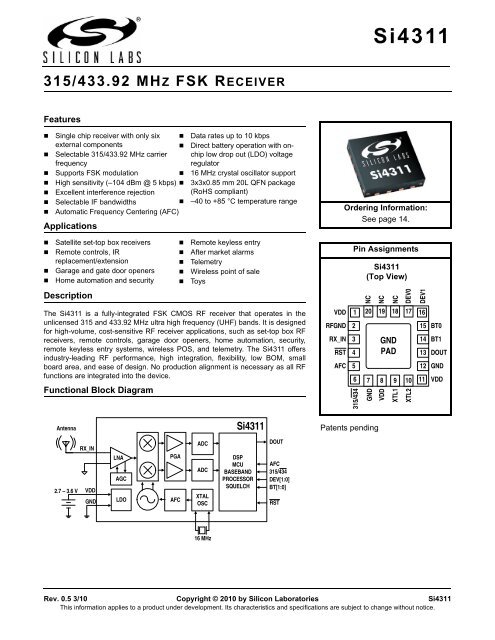
<strong>Si4311</strong><strong>315</strong>/<strong>433.92</strong> MHZ <strong>FSK</strong> RECEIVERFeatures• Single chip receiver with only six • Data rates up to 10 kbpsexternal components• Direct battery operation with onchip• Selectable <strong>315</strong>/<strong>433.92</strong> <strong>MHz</strong> carrierfrequencylow drop out (LDO) voltageregulator• Supports <strong>FSK</strong> modulation• 16 <strong>MHz</strong> crystal oscillator support• High sensitivity (–104 dBm @ 5 kbps) • 3x3x0.85 mm 20L QFN package• Excellent interference rejection (RoHS compliant)• Selectable IF bandwidths• –40 to +85 °C temperature range• Automatic Frequency Centering (AFC)ApplicationsOrdering Information:See page 14.• Satellite set-top box receivers• Remote controls, IRreplacement/extension• Garage and gate door openers• Home automation and securityDescriptionThe <strong>Si4311</strong> is a fully-integrated <strong>FSK</strong> CMOS RF receiver that operates in theunlicensed <strong>315</strong> and <strong>433.92</strong> <strong>MHz</strong> ultra high frequency (UHF) bands. It is designedfor high-volume, cost-sensitive RF receiver applications, such as set-top box RFreceivers, remote controls, garage door openers, home automation, security,remote keyless entry systems, wireless POS, and telemetry. The <strong>Si4311</strong> offersindustry-leading RF performance, high integration, flexibility, low BOM, smallboard area, and ease of design. No production alignment is necessary as all RFfunctions are integrated into the device.Functional Block Diagram• Remote keyless entry• After market alarms• Telemetry• Wireless point of sale• ToysVDDRFGNDRX_INRSTAFCPin Assignments12345201918GNDPAD6 7 8 9<strong>315</strong>/434<strong>Si4311</strong>(Top View)NCNCGNDVDDNCDEV0XTL11710XTL2DEV1161514131211BT0BT1DOUTGNDVDDAntenna<strong>Si4311</strong>Patents pendingRX_IN2.7 – 3.6 V VDDGNDLNAAGCLDOPGAAFCADCADCXTALOSCDSPMCUBASEBANDPROCESSORSQUELCHDOUTAFC<strong>315</strong>/434DEV[1:0]BT[1:0]RST16 <strong>MHz</strong>Rev. 0.5 3/10 Copyright © 2010 by Silicon Laboratories <strong>Si4311</strong>This information applies to a product under development. Its characteristics and specifications are subject to change without notice.
<strong>Si4311</strong>2 Rev. 0.5
<strong>Si4311</strong>1. Electrical SpecificationsTable 1. Recommended Operating Conditions*Parameter Symbol Test Condition Min Typ Max UnitSupply Voltage V DD 2.7 3.3 3.6 VSupply Voltage Powerup Rise Time V DD-RISE 10 — — μsAmbient Temperature T A –40 25 85 °C*Note: All minimum and maximum specifications are guaranteed and apply across the recommended operating conditions.Typical values apply at V DD = 3.3 V and 25 C unless otherwise stated. Parameters are tested in production unlessotherwise stated.Table 2. Absolute Maximum Ratings 1,2Parameter Symbol Value UnitSupply Voltage V DD –0.5 to 3.9 VInput Current 3 I IN 10 mAInput Voltage 3 V IN –0.3 to (V DD + 0.3) VOperating Temperature T OP –45 to 95 CStorage Temperature T STG –55 to 150 CRF Input Level 4 0.4 V PKNotes:1. Permanent device damage may occur if the absolute maximum ratings are exceeded. Functional operation should berestricted to the conditions as specified in the operational sections of this data sheet. Exposure beyond recommendedoperating conditions for extended periods may affect device reliability.2. The <strong>Si4311</strong> device is a high-performance RF integrated circuit with certain pins having an ESD rating of < 2 kV HBM.Handling and assembly of this device should only be done at ESD-protected workstations.3. For input pins <strong>315</strong>/434, AFC, BT[1:0], and DEV[1:0].4. At RF input pin RX_IN.4 Rev. 0.5
<strong>Si4311</strong>Table 3. DC Characteristics(T A = 25 °C, V DD = 3.3 V, R s = 50 Ω, F RF = <strong>433.92</strong> <strong>MHz</strong> unless otherwise noted)Parameter Symbol Test Condition Min Typ Max UnitSupply Current I VDD — 20 — mAReset Supply Current I RST Reset asserted — 2 TBD µAHigh Level Input Voltage 1 V IH 0.7 x V DD — V DD +0.3 VLow Level Input Voltage 1 V IL –0.3 — 0.3 x V DD VHigh Level Input Current 1 I IH V IN =V DD =3.6V –10 — 10 µALow Level Input Current 1 I IL V IN =0V, V DD =3.6V –10 — 10 µAHigh Level Output Voltage 2 V OH I OUT = 500 µA 0.8 x V DD — — VLow Level Output Voltage 2 V OL I OUT = –500 µA — — 0.2 x V DD VNotes:1. For input pins <strong>315</strong>/434, AFC, BT[1:0], and DEV[1:0].2. For output pin DOUT.Table 4. Reset Timing Characteristics(V DD =3.3V, T A =25°C)Parameter Symbol Min Typ Max UnitRST Pulse Width t SRST 100 — — µst SRSTRST70%30%Figure 1. Reset TimingRev. 0.5 5
<strong>Si4311</strong>Table 5. <strong>Si4311</strong> <strong>Receiver</strong> Characteristics(T A =25°C, V DD =3.3V, R s =50Ω, F RF = <strong>433.92</strong> <strong>MHz</strong> unless otherwise noted)Parameter Symbol Test Condition Min Typ Max Unit1.0Sensitivity @ BER = 10-3 (Note 1)kbps, f = 50 kHz, xtal = ±20 ppm,<strong>315</strong> <strong>MHz</strong> (Note 2) — –104 — dBm10 kbps, f = 50 kHz, xtal = ±20 ppm,<strong>315</strong> <strong>MHz</strong> (Note 2) — –101 — dBm1.0 kbps, f = 50 kHz, xtal = ±20 ppm,<strong>433.92</strong> <strong>MHz</strong> (Note 2) — –102 — dBm10 kbps, f = 50 kHz, xtal = ±20 ppm,<strong>433.92</strong> <strong>MHz</strong>TBD –100 — dBmData Rate 3 — — 10 kbpsDesired signal is 3 dB above sensitivity(BER = 10 –3 ), unmodulated interfererAdjacent Channel Rejection±200 kHz 1 is at ±200 kHz, rejection measured as TBD 35 — dBdifference between desired signal andinterferer level in dB when BER = 10 –3Desired signal is 3 dB above sensitivity(BER = 10 –3 ), unmodulated interfererAlternate Channel Rejection±400 kHz 1,2 is at ±400 kHz, rejection measured as — 55 — dBdifference between desired signal andinterferer level in dB when BER = 10 –3Image Rejection, IF = 128 kHz 1,2 — 35 — dBBlocking 1,2±2 <strong>MHz</strong>, 2.4 kbps, desired signal is3 dB above sensitivity, CW interferer — 65 — dBlevel is increased until BER = 10 –3±10 <strong>MHz</strong>, 2.4 kbps, desired signal is3 dB above sensitivity, CW interferer — 70 — dBlevel is increased until BER = 10 –3Maximum RF Input Power 1,2 — 8 — dBmInput IP3 3| f 2 –f 1 | = 5 <strong>MHz</strong>, high gain mode,desired signal is 3 dB above sensitivity,CW interference levels are increased— –10 — dBmuntil BER = 10 –3<strong>FSK</strong> Deviation Input Range 3 10 — 90 kHzLNA Input Capacitance 3 — 7 — pFRX Boot Time 3 From reset — 320 — msNotes:1. 1.0 kbps, f = 50 kHz, xtal = ±20 ppm, AFC = 0, BT[1:0] = 00, DEV[1:0] = 01.2. Guaranteed by characterization.3. Guaranteed by design.6 Rev. 0.5
<strong>Si4311</strong>Table 6. Crystal Characteristics(V DD = 3.3 V, T A =25°C)Parameter Symbol Test Condition Min Typ Max UnitCrystal Oscillator Frequency — 16 — <strong>MHz</strong>Crystal ESR — — 100 XTL1, XTL2 Input Capacitance — 11 — pFRev. 0.5 7
<strong>Si4311</strong>2. Typical Application SchematicDEV0RXANTENNAC3R120 kL1C21 uFVDD12345VDDRFGNDRX_INRSTAFCGNDPAD2019181716NCNCNCDEV0DEV1U1<strong>Si4311</strong>-GM434GNDVDDXTL1XTL2BT0BT1DOUTGNDVDDDEV1BT0BT1151413DOUT1211 VDD VBATTERYC12.7 to 3.6 V22 nF678910AFCX1 (16 <strong>MHz</strong>)Figure 2. <strong>Si4311</strong> <strong>FSK</strong> <strong>433.92</strong> <strong>MHz</strong> Application Schematic2.1. Typical Application Bill of MaterialsTable 7. <strong>Si4311</strong> Typical Application Bill of MaterialsComponent(s) Value/Description Supplier(s)C1 Supply bypass capacitor, 22 nF, 20%, Z5U/X7R MurataC2 Time constant capacitor, 1 µF MurataC3 Antenna matching capacitor, 15 pF MurataL1Antenna matching inductor,33 nH for <strong>433.92</strong> <strong>MHz</strong> and 62 nH for <strong>315</strong> <strong>MHz</strong>MurataR1 Time constant resistor, 20 k MurataX1 16 <strong>MHz</strong> crystal HosonicU1 <strong>Si4311</strong> <strong>315</strong>/<strong>433.92</strong> <strong>MHz</strong> <strong>FSK</strong> receiver Silicon Laboratories8 Rev. 0.5
<strong>Si4311</strong>3.4. Bit Time BT[1:0] SelectionTable 8. Carrier Frequency SelectionPin 6 (<strong>315</strong>/434)Frequency [<strong>MHz</strong>]0 <strong>433.92</strong>1 <strong>315</strong>The <strong>Si4311</strong> can operate with data rates of up to 10 kbps non-return to zero (NRZ) data or 5 kbps Manchesterencoded data. However, <strong>FSK</strong> modulation uses other encoding schemes, such as pulse width modulation (PWM)and pulse position modulation (PPM) in which a bit can be encoded into a pulse with a certain duty cycle or pulsewidth (see Figure 4).Digital Data“1” “0” “1” “1”NRZEncodingManchesterEncodingPPMEncoding1000 usFigure 4. Example Data Waveforms100 usIn order to set the data filter bandwidth correctly, the shortest pulse width of the transmitted encoded data shouldbe chosen as the bit time. In the PPM example shown in Figure 4, the shortest pulse width is 100 µs, so the bit timeis chosen as BT = 100 µs even though the actual data rate is 1 kbps (1000 µs). After finding BT, Table 9 can beused to find the bit settings for pins 14 and 15, BT[1:0]. In this PPM example, BT[1:0] is set as logic BT1 = 1 andBT0 = 1 or BT[1:0] = (1,1) since BT = 100 µs.Table 9. How to Choose BT[1:0] Based on the Bit TimeBit Time [us] BT1 (pin 14) BT0 (pin 15)BT ≥ 1000 0 01000< BT ≤ 500 0 1500 < BT ≤ 200 1 0200 < BT ≤ 100 1 110 Rev. 0.5
3.5. Frequency Deviation Selection<strong>Si4311</strong>In order to accommodate wide frequency deviation ranges, the <strong>Si4311</strong> <strong>FSK</strong> receiver uses two input pins, pins 16and 17, to select a range of frequency deviations as shown in Table 10. For example, if the <strong>FSK</strong> signal has afrequency deviation (F) of 50 kHz, then the DEV[1:0] = (0,1) or pin 16 = 0 and pin 17 = 1.3.6. Automatic Frequency Centering (AFC)Table 10. Frequency Deviation Range SettingsDEV1 (pin 16) DEV0 (pin 17) Frequency Deviation [kHz]0 0 1 < ∆F ≤ 300 1 30 < ∆F ≤ 501 0 50 < ∆F ≤ 701 1 70 < ∆F ≤ 90The channel bandwidth directly affects the sensitivity of any wireless receiver. Typical analog <strong>FSK</strong> receivers use anexternal ceramic filter with a large bandwidth to accommodate the data rate, frequency deviation, crystaltolerances, and transmit carrier frequency offsets, which leads to unnecessary amounts of noise and lowersensitivity levels. The <strong>Si4311</strong> uses a narrow channel bandwidth of 200 kHz and automatic frequency centering(AFC) to obtain excellent sensitivity levels (–104 dBm at data rate of 5 kbps at <strong>315</strong> <strong>MHz</strong>) while still accommodatingup to ±200 kHz of frequency tracking from its center frequency.IF BW200kHzTX OFFSET 100kHzTX OFFSET 100kHz(a)(b)Figure 5. (a) Ideal case (b) Scenario with Tx Offset (c) <strong>Si4311</strong> AFC Re-Centers IF BWIn the ideal case of no transmit carrier frequency errors or receiver frequency errors, both <strong>FSK</strong> tones for a logic "1"and "0" from the transmitter appear in the receiver IF channel bandwidth as shown in Figure 5 (a). However, if thetransmitter has a large carrier offset such as shown in Figure 5 (b), then only one of the <strong>FSK</strong> tones falls in thereceiver channel bandwidth and thus the receiver produces errors. The standard approach to resolving thisproblem is to use an IF channel filter that is large enough to accommodate the transmitter frequency error, but thisleads to degraded sensitivity. The <strong>Si4311</strong> uses AFC to re-center the channel bandwidth about the two <strong>FSK</strong> tonesas shown in Figure 5 (c) to maintain excellent sensitivity with a small IF channel filter. The algorithm requires one<strong>FSK</strong> tone to be in-band and at most three alternating sequences of 0/1 data typically found in a preamble plus700 µs of fixed delay time (approximately 230 µs per 0/1 data pair) to re-center the IF bandwidth. Worst caseacquisition time is 1.3 ms for a data rate of 10 kbps.The AFC algorithm includes a 200 ms hold time. The device holds the frequency found by the AFC algorithm for atime of 200 ms after no RF signal activity before restarting the frequency search. This allows a frequency found inthe first packet of transmission to be held for any subsequent retransmissions of packets if the retransmissionsoccur before 200 ms. This hold frequency ensures all bits of the second and subsequent packets are recoveredcompletely. The AFC frequency search resumes after 200 ms of no RF signal activity.The AFC algorithm can be disabled by setting the logic level on pin 5 to a logic zero as shown in Table 11.(c)Rev. 0.5 11
<strong>Si4311</strong>Table 11. AFC Selection Pin 5Pin 5AFC3.7. Low Noise Amplifier Input CircuitFigure 2 shows the typical application circuit with 50 matching. Components C3 and L1 are used to transform theinput impedance of the LNA. C3 is equal to 15 pF and L1 is equal to 33 nH at <strong>433.92</strong> <strong>MHz</strong> and 62 nH at <strong>315</strong> <strong>MHz</strong>for 50 matching.3.8. Crystal OscillatorAn on-board crystal oscillator is used to generate a 16 <strong>MHz</strong> reference clock for the <strong>Si4311</strong>. This referencefrequency is required for proper operation of the <strong>Si4311</strong> and is used for calibration of the on-chip VCO and othertiming references. No external load capacitors are required to set the 16 <strong>MHz</strong> reference frequency if therecommended crystal load capacitor is around 14 pF, assuming the effective board capacitance between pinsXTL1 and XTL2 is 3 pF and the chip input capacitance on pins XTL1 or XTL2 is 11 pF. Refer to Table 6, “CrystalCharacteristics,” on page 7 for board capacitance and frequency tolerance information. The frequency tolerance ofthe crystal should be chosen such that the received signal is within the IF bandwidth of the <strong>Si4311</strong> receiver.Additionally, the <strong>Si4311</strong> can be driven by an external 16 <strong>MHz</strong> reference clock. The clock signal can be applied toeither the XTL1 or XTL2 inputs. When the 16 <strong>MHz</strong> reference clock is applied to one of the inputs, the other crystalinput pin must be floating.3.9. Reset Pin0 Disable1 EnableDriving the RST pin (pin 4) low will disable the <strong>Si4311</strong> and place the device into reset mode. All active blocks in thedevice are powered off in this mode, bringing the current consumption to
<strong>Si4311</strong>4. Pin Descriptions: <strong>Si4311</strong>-B10-GMNCVDD12019181716RFGND215BT0RX_INRST34GNDPAD1413BT1DOUTAFC512GND6 7 8 91011VDD<strong>315</strong>/434GNDVDDXTL1XTL2NCNCDEV0DEV1Pin Number(s) Name Description1, 8, 11 VDD Supply voltage, may connect to external battery.2 RFGND RF ground. Connect to ground plane on PCB.3 RX_IN RF receiver input.4 RST Device reset, active low input.5 AFC AFC selection input pin.6 <strong>315</strong>/434 Selectable logic input for <strong>315</strong> or <strong>433.92</strong> <strong>MHz</strong> operation.7, 12, GND PAD GND Ground. Connect to ground plane on PCB.9 XTL1 Crystal input.10 XTL2 Crystal input.13 DOUT Data output.14, 15 BT[1:0] Bit time selection input pins.16,17 DEV[1:0] Frequency deviation input pins.18,19,20 NC No connect. Leave floating.Rev. 0.5 13
<strong>Si4311</strong>5. Ordering GuidePart Number* Description PackageType<strong>Si4311</strong>-B10-GM <strong>315</strong>/<strong>433.92</strong> <strong>MHz</strong> <strong>FSK</strong> <strong>Receiver</strong> QFNPb-free*Note: Add an “(R)” at the end of the device part number to denote tape and reel option.OperatingTemperature–40 to 85 °C14 Rev. 0.5
<strong>Si4311</strong>6. Package Markings (Top Marks)6.1. <strong>Si4311</strong> Top Mark6.2. Top Mark ExplanationFigure 6. <strong>Si4311</strong> Top Mark ExampleMark Method:YAG LaserLine 1 Marking: Part Number 11 = <strong>Si4311</strong>Firmware Revision 10 = Firmware Revision 1.0Line 2 Marking: Die Revision B = Revision B DieTTT = Internal Code Internal tracking codeLine 3 Marking: Circle = 0.5 mm Diameter Pin 1 Identifier(Bottom-Left Justified)YWW = Date Code Assigned by the Assembly House. Corresponds to the last digitof the current year (Y) and the workweek (WW) of the molddate.Rev. 0.5 15
<strong>Si4311</strong>7. Package Outline: <strong>Si4311</strong>-B10-GMFigure 7 illustrates the package details for the <strong>Si4311</strong>-B10-GM. Table 12 lists the values for the dimensions shownin the illustration.Figure 7. 20-Pin Quad Flat No-Lead (QFN)Table 12. Package DimensionsSymbol Millimeters Symbol MillimetersMin Nom Max Min Nom MaxA 0.80 0.85 0.90 f 2.53 BSCA1 0.00 0.02 0.05 L 0.30 0.35 0.40b 0.20 0.25 0.30 L1 0.00 — 0.10c 0.27 0.32 0.37 aaa — — 0.05D 3.00 BSC bbb — — 0.05D2 1.65 1.70 1.75 ccc — — 0.08e 0.50 BSC ddd — — 0.10E 3.00 BSC eee — — 0.10E2 1.65 1.70 1.75Notes:1. All dimensions are shown in millimeters (mm) unless otherwise noted.2. Dimensioning and tolerancing per ANSI Y14.5M-1994.16 Rev. 0.5
<strong>Si4311</strong>8. PCB Land Pattern: <strong>Si4311</strong>-B10-GMFigure 8 illustrates the PCB land pattern details for the <strong>Si4311</strong>-B10-GM. Table 13 lists the values for thedimensions shown in the illustration.Figure 8. PCB Land PatternRev. 0.5 17
<strong>Si4311</strong>Table 13. PCB Land Pattern DimensionsSymbol Millimeters Symbol MillimetersMin Max Min MaxD 2.71 REF GE 2.10 —D2 1.60 1.80 W — 0.34e 0.50 BSC X — 0.28E 2.71 REF Y 0.61 REFE2 1.60 1.80 ZE — 3.31f 2.53 BSC ZD — 3.31GD 2.10 —Notes:General1. All dimensions shown are in millimeters (mm) unless otherwise noted.2. Dimensioning and tolerancing is per the ANSI Y14.5M-1994 specification.3. This land pattern design is based on IPC-SM-782 guidelines.4. All dimensions shown are at Maximum Material Condition (MMC). Least MaterialCondition (LMC) is calculated based on a fabrication allowance of 0.05 mm.Solder Mask Design5. All metal pads are to be non-solder-mask-defined (NSMD). Clearance between thesolder mask and the metal pad is to be 60 µm minimum, all the way around the pad.Stencil Design6. A stainless steel, laser-cut and electro-polished stencil with trapezoidal walls shouldbe used to assure good solder paste release.7. The stencil thickness should be 0.125 mm (5 mils).8. The ratio of stencil aperture to land pad size should be 1:1 for the perimeter pads.9. A 1.45 x 1.45 mm square aperture should be used for the center pad. This providesapproximately 70% solder paste coverage on the pad, which is optimum to assurecorrect component standoff.Card Assembly10. A No-Clean, Type-3 solder paste is recommended.11. The recommended card reflow profile is per the JEDEC/IPC J-STD-020 specificationfor small body components.18 Rev. 0.5
<strong>Si4311</strong>DOCUMENT CHANGE LISTRevision 0.1 to Revision 0.2• Maximum data rate changed from 10 to 4 kbps for<strong>FSK</strong> and from 5 to 2 kbps for OOK with Manchesterencoding.• Maximum RF input power changed from 5 to 10dBm.• Changed test conditions for sensitivitymeasurements and added the xtal frequencytolerance of 20 ppm.• Updated text in section “3. Functional Description”.• Added Ideal IF Bandwidth equation and descriptionfor choosing the IF bandwidth in Section “3.4. BitTime BT[1:0] Selection”.• Updated Table 11, “Typical Sensitivity @ 433 <strong>MHz</strong>,2-<strong>FSK</strong>,” on page 11.• Changed hysteresis level from 1 dB to 6 dB inSection “3.8. Crystal Oscillator”.• Added text in section “3.8. Crystal Oscillator”regarding the crystal frequency tolerance and IFBandwidth choice and sensitivity performance.Revision 0.2 to Revision 0.3• Updated features list• Reduced font size in the test condition section ofTable 5 "<strong>Si4311</strong> <strong>Receiver</strong> Characteristics"• Added crystal tolerance equation to Table 6 "CrystalCharacteristics"• Updated matching circuit and BOM to section “2.Test Circuit” and section “2. Typical ApplicationSchematic”• Modified text in Section “3. Functional Description”• Changed bandwidth option in Table 11 "BandwidthSelection Table Using BW[3:1] Pins" and test mode.• Reset section updated to reflect active blocks arepowered off in reset mode.Revision 0.3 to Revision 0.4• Removed crystal frequency tolerance range fromTable 6 "Crystal Characteristics".• Corrected data rates in Section “3.1. Overview”.• Updated text in section “3.4. Bit Time BT[1:0]Selection” to show <strong>FSK</strong> receive IF bandwidthequations.• Deleted voltage gain text in section “3.7. Low NoiseAmplifier Input Circuit”.• Removed squelch circuit description in section “3.8.Crystal Oscillator”.• Included load capacitance requirement for crystal ifno external capacitors are used in section “3.8.Crystal Oscillator”.• Added reset to active time in section “3.9. ResetPin”.• Changed ordering guide part number in section “5.Ordering Guide”.• Added <strong>FSK</strong> Automatic Frequency Calibrationinformation• Removed OOK feature.Revision 0.4 to Revision 0.5• Removed I VDD current spec when input = –30 dBmfrom Table 3 "DC Characteristics"• Updated sensitivity specs and test conditions inTable 5 "<strong>Si4311</strong> <strong>Receiver</strong> Characteristics"• Added AFC hold time description to section “3.6.Automatic Frequency Centering (AFC)”• Added reference clock drive capability to section“3.8. Crystal Oscillator”Rev. 0.5 19
<strong>Si4311</strong>CONTACT INFORMATIONSilicon Laboratories Inc.400 West Cesar ChavezAustin, TX 78701Tel: 1+(512) 416-8500Fax: 1+(512) 416-9669Toll Free: 1+(877) 444-3032Email: wireless@silabs.comInternet: www.silabs.comThe information in this document is believed to be accurate in all respects at the time of publication but is subject to change without notice.Silicon Laboratories assumes no responsibility for errors and omissions, and disclaims responsibility for any consequences resulting fromthe use of information included herein. Additionally, Silicon Laboratories assumes no responsibility for the functioning of undescribed featuresor parameters. Silicon Laboratories reserves the right to make changes without further notice. Silicon Laboratories makes no warranty, representationor guarantee regarding the suitability of its products for any particular purpose, nor does Silicon Laboratories assume any liabilityarising out of the application or use of any product or circuit, and specifically disclaims any and all liability, including without limitation consequentialor incidental damages. Silicon Laboratories products are not designed, intended, or authorized for use in applications intended tosupport or sustain life, or for any other application in which the failure of the Silicon Laboratories product could create a situation where personalinjury or death may occur. Should Buyer purchase or use Silicon Laboratories products for any such unintended or unauthorized application,Buyer shall indemnify and hold Silicon Laboratories harmless against all claims and damages.Silicon Laboratories and Silicon Labs are trademarks of Silicon Laboratories Inc.Other products or brandnames mentioned herein are trademarks or registered trademarks of their respective holders.20 Rev. 0.5