- Page 2 and 3:
Understanding Smart SensorsSecond E
- Page 5:
Library of Congress Cataloging-in-P
- Page 8 and 9:
ContentsPrefacexix1 Smart Sensor Ba
- Page 10 and 11:
Contentsix3.3.3 Hall Effect 603.3.4
- Page 12 and 13:
Contentsxi5.8 Summary 116References
- Page 14 and 15:
Contentsxiii8.3.1 Surface Acoustica
- Page 16 and 17:
Contentsxv11.1.1 Integration and Me
- Page 18 and 19:
Contentsxvii14.4.4 Electrostatic Me
- Page 20 and 21:
PrefaceThe number one challenge fac
- Page 22 and 23:
Prefacexxifor well over 6 years. A
- Page 24 and 25:
2 Understanding Smart Sensorsobserv
- Page 26 and 27:
4 Understanding Smart Sensorssmart
- Page 28 and 29:
6 Understanding Smart Sensorsto pro
- Page 30 and 31:
8 Understanding Smart Sensorsinclud
- Page 32 and 33:
10 Understanding Smart SensorsLevel
- Page 34 and 35:
12 Understanding Smart Sensorsuser
- Page 36 and 37:
14 Understanding Smart Sensorstechn
- Page 38 and 39:
16 Understanding Smart Sensorschang
- Page 40 and 41:
18 Understanding Smart Sensorstechn
- Page 42 and 43:
20 Understanding Smart Sensors Surf
- Page 44 and 45:
22 Understanding Smart Sensorssecon
- Page 46 and 47:
24 Understanding Smart SensorsSilic
- Page 48 and 49:
26 Understanding Smart SensorsSilic
- Page 50 and 51:
28 Understanding Smart SensorsSacri
- Page 52 and 53:
30 Understanding Smart Sensors2.4.3
- Page 54 and 55:
32 Understanding Smart Sensorsmeasu
- Page 56 and 57:
34 Understanding Smart SensorsIon+S
- Page 58 and 59:
36 Understanding Smart Sensorssidew
- Page 60 and 61:
38 Understanding Smart SensorsTable
- Page 62 and 63:
40 Understanding Smart Sensorsoptim
- Page 64 and 65:
42 Understanding Smart SensorsAlumi
- Page 66 and 67:
44 Understanding Smart SensorsThe f
- Page 68 and 69:
46 Understanding Smart Sensors[21]
- Page 70:
This Page Intentionally Left Blank
- Page 73 and 74:
The Nature of Semiconductor Sensor
- Page 75 and 76:
The Nature of Semiconductor Sensor
- Page 77 and 78:
The Nature of Semiconductor Sensor
- Page 79 and 80:
The Nature of Semiconductor Sensor
- Page 81 and 82:
The Nature of Semiconductor Sensor
- Page 83 and 84:
The Nature of Semiconductor Sensor
- Page 85 and 86:
The Nature of Semiconductor Sensor
- Page 87 and 88:
The Nature of Semiconductor Sensor
- Page 89 and 90:
The Nature of Semiconductor Sensor
- Page 91 and 92:
The Nature of Semiconductor Sensor
- Page 93 and 94:
4Getting Sensor Information Into th
- Page 95 and 96:
Getting Sensor Information Into the
- Page 97 and 98:
Getting Sensor Information Into the
- Page 99 and 100:
Getting Sensor Information Into the
- Page 101 and 102:
Getting Sensor Information Into the
- Page 103 and 104:
Getting Sensor Information Into the
- Page 105 and 106:
Getting Sensor Information Into the
- Page 107 and 108:
Getting Sensor Information Into the
- Page 109 and 110:
Getting Sensor Information Into the
- Page 111 and 112:
Getting Sensor Information Into the
- Page 113 and 114:
Getting Sensor Information Into the
- Page 115 and 116:
5Using MCUs/DSPs to Increase Sensor
- Page 117 and 118:
Using MCUs/DSPs to Increase Sensor
- Page 119 and 120:
Using MCUs/DSPs to Increase Sensor
- Page 121 and 122:
Using MCUs/DSPs to Increase Sensor
- Page 123 and 124:
Using MCUs/DSPs to Increase Sensor
- Page 125 and 126:
Using MCUs/DSPs to Increase Sensor
- Page 127 and 128:
Using MCUs/DSPs to Increase Sensor
- Page 129 and 130:
Using MCUs/DSPs to Increase Sensor
- Page 131 and 132:
Using MCUs/DSPs to Increase Sensor
- Page 133 and 134:
Using MCUs/DSPs to Increase Sensor
- Page 135 and 136:
Using MCUs/DSPs to Increase Sensor
- Page 137 and 138:
Using MCUs/DSPs to Increase Sensor
- Page 139 and 140:
Using MCUs/DSPs to Increase Sensor
- Page 141 and 142:
6Communications for Smart SensorsBe
- Page 143 and 144:
Communications for Smart Sensors 12
- Page 145 and 146:
Communications for Smart Sensors 12
- Page 147 and 148:
Communications for Smart Sensors 12
- Page 149 and 150:
Communications for Smart Sensors 12
- Page 151 and 152:
Communications for Smart Sensors 12
- Page 153 and 154:
Communications for Smart Sensors 13
- Page 155 and 156:
Communications for Smart Sensors 13
- Page 157 and 158:
Communications for Smart Sensors 13
- Page 159 and 160:
Communications for Smart Sensors 13
- Page 161 and 162:
Communications for Smart Sensors 13
- Page 163 and 164:
Communications for Smart Sensors 14
- Page 165 and 166:
Communications for Smart Sensors 14
- Page 167 and 168:
Communications for Smart Sensors 14
- Page 169 and 170:
Communications for Smart Sensors 14
- Page 171 and 172:
7Control TechniquesA machine is int
- Page 173 and 174:
Control Techniques 151Table 7.1Type
- Page 175 and 176:
Control Techniques 153otherwise tak
- Page 177 and 178:
Control Techniques 155consisting of
- Page 179 and 180:
Control Techniques 157Supplied byap
- Page 181 and 182:
Control Techniques 159InputX1Synaps
- Page 183 and 184:
Control Techniques 1617.6 Adaptive
- Page 185 and 186:
Control Techniques 163ObserverHB−
- Page 187 and 188:
Control Techniques 165linear-vector
- Page 189 and 190:
Control Techniques 1677.7.2 Combine
- Page 191 and 192:
Control Techniques 169Domain-type s
- Page 193 and 194:
Control Techniques 171[19] De Silva
- Page 195 and 196:
8Transceivers, Transponders, andTel
- Page 197 and 198:
Transceivers, Transponders, and Tel
- Page 199 and 200:
Transceivers, Transponders, and Tel
- Page 201 and 202:
Transceivers, Transponders, and Tel
- Page 203 and 204:
Transceivers, Transponders, and Tel
- Page 205 and 206:
Transceivers, Transponders, and Tel
- Page 207 and 208:
Transceivers, Transponders, and Tel
- Page 209 and 210: Transceivers, Transponders, and Tel
- Page 211 and 212: Transceivers, Transponders, and Tel
- Page 213 and 214: Transceivers, Transponders, and Tel
- Page 215 and 216: Transceivers, Transponders, and Tel
- Page 217 and 218: Transceivers, Transponders, and Tel
- Page 219 and 220: Transceivers, Transponders, and Tel
- Page 221 and 222: Transceivers, Transponders, and Tel
- Page 223 and 224: 9MEMS Beyond Sensors“And these ot
- Page 225 and 226: MEMS Beyond Sensors 203would not ex
- Page 227 and 228: MEMS Beyond Sensors 205PyrexSilicon
- Page 229 and 230: MEMS Beyond Sensors 207(a)IFluxIIMa
- Page 231 and 232: MEMS Beyond Sensors 209InletThermop
- Page 233 and 234: MEMS Beyond Sensors 211Figure 9.8 A
- Page 235 and 236: MEMS Beyond Sensors 2139.3.2 Microo
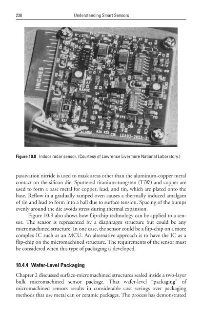
- Page 237 and 238: MEMS Beyond Sensors 215Over-range p
- Page 239 and 240: MEMS Beyond Sensors 217+ 10°− 10
- Page 241 and 242: MEMS Beyond Sensors 219achieved wit
- Page 243 and 244: MEMS Beyond Sensors 221Methods for
- Page 245 and 246: MEMS Beyond Sensors 223Figure 9.19
- Page 247 and 248: MEMS Beyond Sensors 225[21] Tortone
- Page 249 and 250: 10Packaging, Testing, and Reliabili
- Page 251 and 252: Packaging, Testing, and Reliability
- Page 253 and 254: Packaging, Testing, and Reliability
- Page 255 and 256: Packaging, Testing, and Reliability
- Page 257 and 258: Packaging, Testing, and Reliability
- Page 259: Packaging, Testing, and Reliability
- Page 263 and 264: Packaging, Testing, and Reliability
- Page 265 and 266: Packaging, Testing, and Reliability
- Page 267 and 268: Packaging, Testing, and Reliability
- Page 269 and 270: Packaging, Testing, and Reliability
- Page 271 and 272: 11Mechatronics and Sensing SystemsP
- Page 273 and 274: Mechatronics and Sensing Systems 25
- Page 275 and 276: Mechatronics and Sensing Systems 25
- Page 277 and 278: Mechatronics and Sensing Systems 25
- Page 279 and 280: Mechatronics and Sensing Systems 25
- Page 281 and 282: Mechatronics and Sensing Systems 25
- Page 283 and 284: Mechatronics and Sensing Systems 26
- Page 285 and 286: Mechatronics and Sensing Systems 26
- Page 287 and 288: Mechatronics and Sensing Systems 26
- Page 289 and 290: Mechatronics and Sensing Systems 26
- Page 291 and 292: Mechatronics and Sensing Systems 26
- Page 293 and 294: Mechatronics and Sensing Systems 27
- Page 295 and 296: 12Standards for Smart SensingThe la
- Page 297 and 298: Standards for Smart Sensing 275Netw
- Page 299 and 300: Standards for Smart Sensing 277NCAP
- Page 301 and 302: Standards for Smart Sensing 279Proc
- Page 303 and 304: Standards for Smart Sensing 281PID
- Page 305 and 306: Standards for Smart Sensing 283•
- Page 307 and 308: Standards for Smart Sensing 285•
- Page 309 and 310: Standards for Smart Sensing 287Tabl
- Page 311 and 312:
Standards for Smart Sensing 289perf
- Page 313 and 314:
Standards for Smart Sensing 2911 0
- Page 315 and 316:
Standards for Smart Sensing 293obje
- Page 317 and 318:
Standards for Smart Sensing 295Mult
- Page 319 and 320:
13The Implications of Smart SensorS
- Page 321 and 322:
The Implications of Smart Sensor St
- Page 323 and 324:
The Implications of Smart Sensor St
- Page 325 and 326:
The Implications of Smart Sensor St
- Page 327 and 328:
The Implications of Smart Sensor St
- Page 329 and 330:
The Implications of Smart Sensor St
- Page 331 and 332:
The Implications of Smart Sensor St
- Page 333 and 334:
14The Next Phase of Sensing Systems
- Page 335 and 336:
The Next Phase of Sensing Systems 3
- Page 337 and 338:
The Next Phase of Sensing Systems 3
- Page 339 and 340:
The Next Phase of Sensing Systems 3
- Page 341 and 342:
The Next Phase of Sensing Systems 3
- Page 343 and 344:
The Next Phase of Sensing Systems 3
- Page 345 and 346:
The Next Phase of Sensing Systems 3
- Page 347 and 348:
The Next Phase of Sensing Systems 3
- Page 349 and 350:
The Next Phase of Sensing Systems 3
- Page 351 and 352:
The Next Phase of Sensing Systems 3
- Page 353 and 354:
The Next Phase of Sensing Systems 3
- Page 355 and 356:
List of Acronyms and Abbreviations3
- Page 357 and 358:
List of Acronyms and Abbreviations
- Page 359 and 360:
List of Acronyms and Abbreviations
- Page 361 and 362:
List of Acronyms and Abbreviations
- Page 363 and 364:
List of Acronyms and Abbreviations
- Page 365 and 366:
List of Acronyms and Abbreviations
- Page 367 and 368:
List of Acronyms and Abbreviations
- Page 369 and 370:
List of Acronyms and Abbreviations
- Page 371 and 372:
List of Acronyms and Abbreviations
- Page 373 and 374:
Glossaryablationvaporization of mat
- Page 375 and 376:
Glossary 353buscalibrationconnectio
- Page 377 and 378:
Glossary 355end point straight line
- Page 379 and 380:
Glossary 357data transmission and p
- Page 381 and 382:
Glossary 359multiplexer device that
- Page 383 and 384:
Glossary 361repeatability the maxim
- Page 385 and 386:
Glossary 363spread spectrum techniq
- Page 387 and 388:
Glossary 365transducer a device con
- Page 389 and 390:
Selected BibliographyBooks and Jour
- Page 391 and 392:
Selected Bibliography 369Northeaste
- Page 393 and 394:
Selected Bibliography 371Miscellane
- Page 395 and 396:
About the AuthorRandy Frank is a te
- Page 397 and 398:
Index4-to 20-mA signal transmitter,
- Page 399 and 400:
Index 377definitions, 119-20introdu
- Page 401 and 402:
Index 379HVAC, 318-19MCU with integ
- Page 403 and 404:
Index 381Linearization, 108Linear p
- Page 405 and 406:
Index 383in chemical measurements,
- Page 407 and 408:
Index 385Ratiometricity, 56Reactive
- Page 409 and 410:
Index 387IC fabrication, 19micromec
- Page 411:
Index 389Transducer-independent int


![monografia [arquivo *.pdf 5,3 Mb] - Nomads.usp](https://img.yumpu.com/42117980/1/190x135/monografia-arquivo-pdf-53-mb-nomadsusp.jpg?quality=85)