section 7 - Index of
section 7 - Index of section 7 - Index of
While the PLL is regaining lock, the CKOUT clock output remains at the same logic levelit held when the PLL lost lock, which is when the clocks were frozen in the DSP.When the chip enters the WAIT processing state, the core phases are disabled but CKOUT continues to operate. When PLL is disabled, CKOUT will be fed from EXT AL.If DF> 1 and CKOS*CSRC, then the programmer must change either CKOS or CSRC beforetaking any action that causes the PLL to lose and subsequently regain lock, such aschanging the multiplication factor, enabling PLL operation, or recovering from the STOPstate with PSTP=O.Any change of the CKOS or CSRC bits must be done while DF=1.9.4.9 Synchronization Among EXTAL, CKOUT, and the Internal ClockLow clock skew between EXTAL and CKOUT is guaranteed only if MF:$;4. The synchronizationbetween CKOUT and the internal chip activity and Port A timing is guaranteed inall cases where CKOS=CSRC and the bits have never differed from one another.-
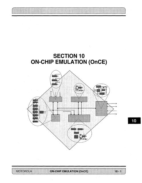
SECTION 10ON-CHIP EMULATION (OnCE)-
- Page 140 and 141: Table 7-2 Status Register Interrupt
- Page 142 and 143: 7.3.3 Interrupt SourcesInterrupts c
- Page 144 and 145: interrupts makes it very useful for
- Page 146 and 147: MAINPROGRAMFETCHESLONG INTERRUPTSER
- Page 148 and 149: 7.3.3.3 Other Interrupt SourcesOthe
- Page 150 and 151: 7.3.4 Interrupt ArbitrationInterrup
- Page 152 and 153: 7.3.7 Interrupt Instruction Executi
- Page 154 and 155: MAINPROGRAMMEMORYINTERRUPT SYNCHRON
- Page 156 and 157: MAINPROGRAMFETCHESINTERRUPTSYNCHRON
- Page 158 and 159: MAINPROGRAMFAST INTERRUPTVECTORLONG
- Page 160 and 161: MAINPROGRAMFETCHESNTERRUPTSYN8HRCNZ
- Page 162 and 163: 7.5 WAIT PROCESSING STATEThe WAIT i
- Page 164 and 165: The stop processing state halts all
- Page 166 and 167: the first instruction fetch). If th
- Page 168: RESET -----------------------------
- Page 172 and 173: 16 - BIT INTERNALADDRESS BUSESX ADD
- Page 174 and 175: 8.2.2.1 Address (AO-A15)These three
- Page 177: SECTION 9PLL CLOCK OSCILLATOR-
- Page 180 and 181: X MEMORYRAM/ROMEXPANSION24-Bit56KMo
- Page 182 and 183: 23 22 21 20 19 18 17 16 15 14 13 12
- Page 184 and 185: cleared. To enable rapid recovery w
- Page 186 and 187: -CLVCCVCC for the CKOUT output. The
- Page 188 and 189: 4. For all input frequencies which
- Page 193 and 194: 10.1 ON-CHIP EMULATION INTRODUCTION
- Page 195 and 196: 10.2.2 Debug Serial Clock/Chip Stat
- Page 197 and 198: 76543210I R/W I GO I EX I RS41 RS31
- Page 199 and 200: shifted in (so a new command is ava
- Page 201 and 202: 10.3.4.4 Software Debug Occurrence
- Page 203 and 204: 10.4.4 Memory High Address Comparat
- Page 205 and 206: 10.6.1 External Debug Request Durin
- Page 207 and 208: PABCIRCULARBUFFERPOINTERDSCKDSOFigu
- Page 209 and 210: are serially available to the exter
- Page 211 and 212: k. ACKI. ClKm. Send command READ FI
- Page 213 and 214: 19. ACK20. Send command READ GDB RE
- Page 215 and 216: 10.11.6.1 Case 1: Return To The Pre
- Page 217: SECTION 11ADDITIONAL SUPPORTDr. BuB
- Page 220 and 221: The following is a partial list of
- Page 222 and 223: • In-line assembler language code
- Page 224 and 225: I Document 10 I Version Synopsis I
- Page 226 and 227: I Document 10 I Version Synopsis I
- Page 228 and 229: I Document ID I Version Synopsis I
- Page 230 and 231: I Document 10 I Version Synopsis I
- Page 232 and 233: 11.5 MOTOROLA DSP NEWSThe Motorola
- Page 234 and 235: DIGITAL SIGNAL PROCESSINGAlan V. Op
- Page 236 and 237: C Programming Language:Controls:. C
- Page 238 and 239: Image Processing:DIGITAL IMAGE PROC
SECTION 10ON-CHIP EMULATION (OnCE)-


