EE462L, Power Electronics, DC-DC Buck/Boost Converter ... - ECS
EE462L, Power Electronics, DC-DC Buck/Boost Converter ... - ECS
EE462L, Power Electronics, DC-DC Buck/Boost Converter ... - ECS

You also want an ePaper? Increase the reach of your titles
YUMPU automatically turns print PDFs into web optimized ePapers that Google loves.
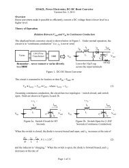
<strong>EE462L</strong>, <strong>Power</strong> <strong>Electronics</strong>, <strong>DC</strong>-<strong>DC</strong> <strong>Buck</strong>/<strong>Boost</strong> <strong>Converter</strong>Version Oct. 10, 2011Overview<strong>Buck</strong>/<strong>Boost</strong> converters make it possible to efficiently convert a <strong>DC</strong> voltage to either a lower orhigher voltage. <strong>Buck</strong>/<strong>Boost</strong> converters are especially useful for PV maximum power trackingpurposes, where the objective is to draw maximum possible power from solar panels at all times,regardless of the load.Theory of OperationRelation Between V out and V in in Continuous ConductionThe idealized buck/boost converter circuit is shown below in Figure 1. Under normal operation,the circuit is in “continuous conduction” (i.e., i L1 and i L2 are always greater than zero).VariacI in+ v L1−i L1+ v C1−i C1i dI out120/25VacTransformer DBR V inL1C 1L 2+v L2–i L2Ci C+V out–Remember – never connect avariac directly to a DBR!Leave the 10µF cap acrossthe input terminals0.01ΩFigure 1. <strong>DC</strong>-<strong>DC</strong> <strong>Buck</strong>/<strong>Boost</strong> <strong>Converter</strong>The first important relationship comes from the fact that capacitor C 1 should be large enough sothat voltage v C1has low ripple. Applying average KVL around the loop formed by V in , L 1 , C 1 ,and L 2 , and recognizing that the average voltages across L 1 and L 2 are each zero, yieldsv C1 = V in . (1)The second important relationship comes by applying KCL in the average sense at the node atopL 2 . Since the average currents in C 1 and C are both zero, theni L avg = idavg= Iout2 . (2)With continuous conduction, the circuit has two states – switch closed, and switch open. Thesestates are shown in Figures 2a and 2b.Page 1 of 12
<strong>EE462L</strong>, <strong>Power</strong> <strong>Electronics</strong>, <strong>DC</strong>-<strong>DC</strong> <strong>Buck</strong>/<strong>Boost</strong> <strong>Converter</strong>Version Oct. 10, 2011V in(V out + V in )– – +L 1 V in L C +C 2+ 1V out–L 1 chargingC 1 dischargingL 2 chargingC dischargingFigure 2a. Switch Closed for DT SecondsV inL 1V in+ – L 1 dischargingC 1L 2Figure 2b. Switch Open for (1-D)T SecondsC+V out–C 1 chargingL 2 dischargingC chargingWhen the switch is closed (Figure 2a), the diode is reverse biased and open, current i L1increases at the rate ofdi L 1 Vin= , ≤ t ≤ DTdt L10 , (3)so that L 1 is “charging.” When the switch is open (Figure 2b), the diode is forward biased, andi L decreases at the rate ofdiL1dt−VoutL1= , DT < t < T , (4)so that L 1 is “discharging.” The voltage across L 1 is shown in Figure 3.V in0− V outFigure 3. Inductor L 1 Voltage in Continuous ConductionBecause of the steady-state inductor principle, the average voltage across L 1 is zero. Since v L1has two states, both having constant voltage, the average value of v L1isPage 2 of 12
<strong>EE462L</strong>, <strong>Power</strong> <strong>Electronics</strong>, <strong>DC</strong>-<strong>DC</strong> <strong>Buck</strong>/<strong>Boost</strong> <strong>Converter</strong>Version Oct. 10, 2011( 1−D)VoutV( D)outΔ I1= • 1−T =, (8)L1L1fwhere f is the switching frequency.The boundary of continuous conduction for L 1 is whenTi L1 min = 0, as shown in Figure 5.Δ I 1iL1 max = 2I L 1avgi L1avg = Iini L1 min = 0DT(1–D)TFigure 5. Inductor L1 Current at the Boundary of Continuous ConductionThus, at the boundary,2Iin( 1−D)Vout= , (9)L f1boundaryso that( 1−D) DV ( 1−D)VoutinDV inL1 boundary = = • = . (10)2Iinf 1−D 2Iinf 2IinfAs D approaches unity,VinL1 > 2Iinf(11)will guarantee continuous conduction. Note in (10) and (11) that continuous conduction can beachieved more easily when I in and f are large.Page 4 of 12
<strong>EE462L</strong>, <strong>Power</strong> <strong>Electronics</strong>, <strong>DC</strong>-<strong>DC</strong> <strong>Buck</strong>/<strong>Boost</strong> <strong>Converter</strong>Version Oct. 10, 2011so thatL2boundary( 1−D)Vout= . (14)2IoutfSince the maximum value of (14) occurs at D → 0,VoutL2 > (15)2Ioutfwill guarantee continuous conduction for L2 for all D. Note in (14) and (15) that continuousconduction can be achieved more easily when I out and f are large.Current Ratings for Continuous Conduction OperationContinuous current waveforms for the MOSFET, the capacitors, and the diode in continuousconduction are shown in Figure 8 on the following page. Corresponding waveforms for theinductors were shown previously in Figures 4 and 6.Following the same formulas and reasoning used for the buck converter, conservative currentratings for components L1, L2, the MOSFET, and the diode follow.For L1, using Figure 5,2⎛ ⎞=2 1 +2 1I L1,rms,maxIin( 2Iin) = Iin2 ⎜1+ ⎟ ,12⎝ 3 ⎠so that2I L I31 , rms,max= in . (16)Similarly, for L2, using Figure 7,2I L I32 , rms,max= out . (17)Page 6 of 12
<strong>EE462L</strong>, <strong>Power</strong> <strong>Electronics</strong>, <strong>DC</strong>-<strong>DC</strong> <strong>Buck</strong>/<strong>Boost</strong> <strong>Converter</strong>Version Oct. 10, 2011i L1 + iL2MOSFETΔ I1 + ΔI 2I in + I out0DTi L1C 1Δ I 1I in0Δ I 2out− I− i L2i L1 + iL2DiodeΔ I1 + ΔI 2I in + Iout0iL 1 + iL2− IoutCΔ I1 + ΔI 2I in0−Figure 8. Current Waveforms for MOSFET, Capacitors, and Diode in Continuous ConductionI outPage 7 of 12
<strong>EE462L</strong>, <strong>Power</strong> <strong>Electronics</strong>, <strong>DC</strong>-<strong>DC</strong> <strong>Buck</strong>/<strong>Boost</strong> <strong>Converter</strong>Version Oct. 10, 2011For the MOSFET and diode, assuming large worst-case D, and using Figure 8,2I = +32I = +3( I I )MOSFET , rms,maxin out , (18)( I I )Diode, rms,maxin out . (19)For C1 and C, using Figure 8,2I C I32I31 , rms,max= in or out, whichever is larger. (20)2I C I3, rms,max= in or outI , whichever is larger. (21)Voltage Ratings for Continuous Conduction OperationReferring to Figure 2b, when the MOSFET is open, it is subjected to (Vin + Vout). Because ofthe usual double-voltage switching transients, the MOSFET should therefore be rated2(Vin+Vout).Referring to Figure 2a, when the MOSFET is closed, the diode is subjected to (Vin + Vout). Thediode should be rated at 2(Vin+Vout).Note – “stiff” voltages across capacitors C1 and C will help hold down overshoots on theMOSFET and diode in this circuit.Output Capacitor Voltage RippleThe maximum ripple voltage calculation for output capacitor C follows from Figure 8 and is thesame as for the boost converter, namelyΔQIoutDT IoutDΔ V = = = .C C CfThe maximum peak-to-peak ripple thus occurs as D → 1 and isIoutΔVmax = . (22)CfComparing the current graphs for C 1 and C in Figure 8 during the DT “switch closed” period, itcan be seen graphically that the ripple voltage on C 1 and C are the same, i.e. Equation (22).Page 8 of 12
<strong>EE462L</strong>, <strong>Power</strong> <strong>Electronics</strong>, <strong>DC</strong>-<strong>DC</strong> <strong>Buck</strong>/<strong>Boost</strong> <strong>Converter</strong>Version Oct. 10, 2011The ExperimentImportant – to avoid excessive output voltages, always keep a load attached to theconverter when it is operating. Do not exceed 90V on the converter output.1. Reconfigure the buck or boost components according to Figure 1 in this document.Secure new components C 1 and L 2 . Make all connections. Capacitor C 1 is bipolar (i.e.,not polarized).2. Connect the MOSFET Firing Circuit to your converter, using short leads. The firingcircuit is the same as for the <strong>Boost</strong> <strong>Converter</strong>. Double check your range of D.3. Before connecting power, make sure that a 5Ω ceramic power resistor is connected asa load. View V GS on Channel #1, adjust D to the minimum setting, and F toapproximately 100kHz. Connect Channel #2 to view V DS . Set the trigger for Channel#1.Important Note: the first time you energize your converter, feed the 120/25V transformerthrough a variac, so that you can SLOWLY increase the voltage from zero and read thevariac ammeter to detect short circuits before they become serious. A common problem isto have the MOSFET in backward, so that its internal antiparallel diode creates a short circuit.The ammeter on the variac is an excellent diagnostic tool. Once you are convinced that yourcircuit is working correctly, the variac is then optional. Remember – your boost converterrequires <strong>DC</strong> input power from a DBR.Does your circuit have a short? If so, do the following:1. Make sure that your MOSFET is not connected backwards.2. Observe VGS on the MOSFET as you vary D and F. Does the waveform look correct?3. Unplug the wall wart. Does the short circuit go away? If not, your MOSFET may beshorted – so, disconnect the MOSFET from the converter, and perform the voltagecontrolledresistance test on the MOSFET.4. Connect a 25Vac transformer to a DBR. Connect the DBR to your buck/boost converter,keeping the wires short (i.e., 3” or less). Then, use a variac to energize the 25Vactransformer and DBR. Raise the variac until Vac of the transformer is approximately 27-28V.5. Use a 5Ω ceramic power resistor as a load. With F ≈ 100kHz, slowly increase D fromits smallest value to obtain V out = 10, 20 (within ±2V), while recording D, Vin , Vout,Iin , Iout. Note by viewing V DS whether or not the circuit is in continuous currentoperation. For the 20V condition, compute input and output powers and efficiency. Donot go above 20V with the 5Ω load.Page 9 of 12
<strong>EE462L</strong>, <strong>Power</strong> <strong>Electronics</strong>, <strong>DC</strong>-<strong>DC</strong> <strong>Buck</strong>/<strong>Boost</strong> <strong>Converter</strong>Version Oct. 10, 2011Appendix<strong>Converter</strong>Type<strong>Buck</strong><strong>Boost</strong><strong>Buck</strong>/<strong>Boost</strong>Worst-Case Component Ratings Comparisons for <strong>DC</strong>-<strong>DC</strong> <strong>Converter</strong>sOutputInput Inductor Capacitor Output Capacitor Diode andCurrent (Arms) Voltage Current (Arms) MOSFET Voltage2 1.5VI out1 2VoutI inout332 1.5V I outI out2Voutin32 1.5VI out ⎛ 2 ⎞ 2 ( V in + V )inmax ⎜ I in , I ⎟out3out⎝ 3 ⎠Diode andMOSFETCurrent (Arms)2I out32I in323( I in + I out )Series CapacitorVoltage1.5VinAdditional Components for <strong>Buck</strong>/<strong>Boost</strong> <strong>Converter</strong>Series CapacitorSeries Capacitor (C 1 ) (C 1 ) RippleCurrent (Arms) Voltage (peak-topeak)⎛ 2 2 ⎞ Imax ⎜ I in , I out ⎟out⎝ 3 3 ⎠ C1fComparisons of Output Capacitor Ripple Voltage<strong>Converter</strong> TypeVolts (peak-to-peak)<strong>Buck</strong>I out4Cf<strong>Boost</strong>I outCf<strong>Buck</strong>/<strong>Boost</strong>I outCfSecond Inductor(L 2 ) Current(Arms)23I outPage 11 of 12
<strong>EE462L</strong>, <strong>Power</strong> <strong>Electronics</strong>, <strong>DC</strong>-<strong>DC</strong> <strong>Buck</strong>/<strong>Boost</strong> <strong>Converter</strong>Version Oct. 10, 2011Minimum Inductance Values Needed to Guarantee Continuous Current<strong>Converter</strong> Type For Continuous Currentin the Input InductorFor ContinuousCurrent in L2<strong>Buck</strong>VoutL >2Ioutf–<strong>Boost</strong>VinL >2Iinf–<strong>Buck</strong>/<strong>Boost</strong>VinL1 VoutL2 2If2IfinoutPage 12 of 12