ENSONIQ SIGNAL PROCESSOR 2 - ESP2 - Freeverb3
ENSONIQ SIGNAL PROCESSOR 2 - ESP2 - Freeverb3
ENSONIQ SIGNAL PROCESSOR 2 - ESP2 - Freeverb3

Create successful ePaper yourself
Turn your PDF publications into a flip-book with our unique Google optimized e-Paper software.
<strong>ESP2</strong><strong>ENSONIQ</strong> <strong>SIGNAL</strong> <strong>PROCESSOR</strong> 2Part IInstruction and Hardware Specification1995David AndreasJon DattorroJ. William Mauchly
0. Introduction.................................................................................................................51. Chip Overview..............................................................................................................61.1. Chip Architecture .........................................................................................71.1.1. Function Units: MAC, ALU, AGEN................................................81.1.2. Internal Registers. .........................................................................8Table 1. Internal Register Address Map..................................................81.1.3. GPR and AOR.................................................................................91.1.4. SPR ................................................................................................91.1.5. Internal Register Usage .................................................................10Table 2. Registers as Operands ...............................................................101.1.6. Instruction Memory.......................................................................101.1.7. Future Expandability .....................................................................101.1.8. Internal Operand Busses ...............................................................101.1.9. External Interfaces ........................................................................111.2. Instruction Cycle Timing...............................................................................121.3. Latency .........................................................................................................131.3.1. Inter-Unit Latency.........................................................................131.3.2. Latency of External Memory Access via AGEN .............................132. Multiplier/Accumulator/Shifter ...................................................................................152.1. Architecture..................................................................................................152.1.1. Exception Processing .....................................................................17Table 3. Multiplier Exceptions.................................................................172.2. MAC unit Barrel Shifter ...............................................................................172.3. Accessing the MAC unit ................................................................................172.3.1. Writing the MACP (Preload) latch.................................................182.3.2. Reading the MAC latch .................................................................182.3.3. MAC Result Low latch (MACRL)....................................................182.4. MAC unit Instructions ..................................................................................19Table 4. MAC unit List of Instructions ....................................................192.5. MAC unit Pseudo Instructions......................................................................203. ALU and Instruction Set .............................................................................................243.1. ALU Instructions ..........................................................................................253.2. ALU Pseudo Instructions..............................................................................423.3. Condition Code Register ...............................................................................483.3.1. Setting Condition Codes.................................................................49Table 5. CCR Setting by Instruction........................................................493.3.2. Conditional Execution Mechanism .................................................513.3.3. Instructions Not Skippable ............................................................523.3.4. Arithmetic Condition Masking .......................................................52Table 6. Arithmetic Condition Code Masks .............................................533.4. Instruction Cycle Execution Latency (Latent Instructions)..........................544. Indirect Register Addressing.......................................................................................584.1. Exceptions to Indirection..............................................................................59Table 7. Indirection Operand Availability................................................594.2. Pointer Register Latencies............................................................................605. Internal Memory Refresh............................................................................................615.1. Instruction Refresh.......................................................................................615.2. GPR and AOR Refresh..................................................................................615.2.1. Internal Register Refresh during Suspension/Halt ........................625.2.2. Internal Register Refresh Collision................................................626. SPR Hazards................................................................................................................63
7. External Data-Memory Interface ................................................................................647.1. Address Generator (AGEN) Architecture.....................................................647.1.1. AGEN Address Calculation............................................................657.1.2. Plus-One Addressing Mode ............................................................657.1.3. Extent of the Modulo .....................................................................667.1.4. Other External Memory Configurations ........................................667.1.5. UPDATE region BASE...................................................................667.2. AGEN Instructions ......................................................................................677.3. Accessing the Region Control Registers and AORs.......................................677.4. External Memory Access ..............................................................................677.4.1. External Address Buss...................................................................69Table 8. External Address Pin Connection ..............................................697.4.2. External Memory Data-Interface...................................................707.5. External DRAM Refresh...............................................................................717.6. Initializing or Accessing External Memory from the System Host...............728. Serial Interface............................................................................................................738.1. Serial Interface Control Registers................................................................73Table 9. Serial Interface Control Registers .............................................738.2. LRCLK ..........................................................................................................748.3. WCLK ...........................................................................................................748.4. BCLK ............................................................................................................758.5. An Example of Serial Interface Control Register Settings ...........................758.6. Serial Interface Rules ...................................................................................778.7. Serial Reset and Synchronization.................................................................779. Halt and Suspension States.........................................................................................789.1. Halting the Chip............................................................................................789.2. Chip State during Halt and Suspension........................................................789.3. Single Step Mode..........................................................................................809.4. Single Pass Operation...................................................................................8010. Chip Reset, Initialization, and Synchronization.........................................................8110.1. Reset ...........................................................................................................8110.2. Initialization................................................................................................8210.3. Synchronization...........................................................................................83Table 10. SYNC_MODE bit functionality.................................................8311. Special Purpose Registers..........................................................................................8411.1 SPR Descriptions .........................................................................................8912. Host/<strong>ESP2</strong> Interface ..................................................................................................9312.1. Host/<strong>ESP2</strong>-Register Interface.....................................................................9412.1.1. Writing GPR/AOR/SPR.................................................................9412.1.2. Reading GPR/AOR/SPR ................................................................9412.2. Host/<strong>ESP2</strong>-Instruction Interface ................................................................9512.2.1. Writing Instruction Memory........................................................9512.2.2. Reading Instruction Memory........................................................9512.3. Host Interface Registers.............................................................................9612.3.1. Testing..........................................................................................9612.3.2. Some Host Interface Register Descriptions .................................9913. Pin List.......................................................................................................................100Table 11. <strong>ESP2</strong> Chip Pinout ................................................................................1013
MISSING INFORMATION:Serial, external memory, and host interfaces; setup & hold times.Recommend pull-up resistor values.4
0. IntroductionThe demands of digital audio require particular features from DSP (Digital SignalProcessing) chips for sound-effect design. The semiconductor industry serves a broadercustomer base, however. While several commercial processor chips are more or lesssuitable to the audio technical community, this is not what drives digital audio-basedcompanies into the intense and expensive design cycle of custom VLSI. The principaldriving force is the competitive edge gained by proprietary hardware which stifles reverseengineering. The primary end-product, of course, is software; the algorithms which drivethe chips.To remain competitive with contemporary products, a typical commercial sound-effectsbox needs to execute roughly 30 different algorithm types, each satisfying certain artisticstandards of quality. While in the throes of an audio signal processor design, a DSP gurufrom CCRMA, Stanford University, theorized that most DSP algorithms can beformulated in terms of the digital filter. [Moorer] Reverberation algorithm design,however, remains more of an artistic endeavor than a science; this elusive specialty is stilldominated by a few companies having the benefit of an early start. [Blesser/Bader][Griesinger]Having this mandate, three design engineers were given carte blanche in 1990 to improveupon an existing and proven chip design known as ESP. Rarely does an audio-productspecification call for the algorithm designers to engineer the computer as well. Theoutcome is the fixed-point <strong>ESP2</strong> which, as it turns out, exceeds the capabilities ofcommercial DSP chips with regard to audio processing efficiency.The purpose of Part I, the Hardware (or Chip) Specification, is to explain the <strong>ESP2</strong> chipdesign philosophy as it pertains to DSP applied to audio. The <strong>ESP2</strong> programmingLanguage is discussed in Part II, often referred to as the Software Specification. Wediscuss effect design and present algorithms for several practical and real AudioApplications in Part III. We do this, first, to highlight the efficiency of the <strong>ESP2</strong>, second,as an exposition of how fundamental DSP operations are accomplished in real-time, third,to present some new results in the field of audio and DSP.5
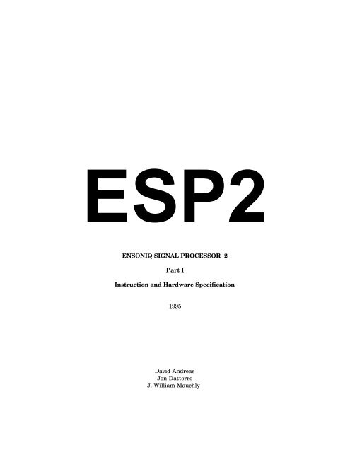
1. Chip OverviewPart I fully explains the functionality of the Digital Signal Processor chip called <strong>ESP2</strong>. Toassist the programmer, this Chip Spec. explains the implementation of all the <strong>ESP2</strong>instructions. The information required by the engineer to design this chip into somesystem is also found here, and is explained so as to be accessible to programmers having alimited hardware background.The information regarding the instructions is supplemented in Part II, the Language andSoftware Spec., which explains nuances of the syntax which is the <strong>ESP2</strong> assemblylanguage. The <strong>ESP2</strong> language resembles some aspects of the C programming language.The language is easy to learn, intuitive, and truly a step up from the standard practice ofmanipulating unmeaningful register names.The Software Spec. should be read by anyone using the <strong>ESP2</strong> for intensive operationsinvolving external memory access (e.g., Reverberator design). Other engineers wishing towrite simpler test programs can get by with Part I and an example of a complete <strong>ESP2</strong>program from which they may derive a shell to work within. Programming examples canbe found in the Applications section, Part III. The References are found thereafter.The <strong>ESP2</strong> chip architecture, shown in Figure 1, is optimized for the processing of audiosignals. The demands of audio dictate a minimum single precision bit-width of 24 bits.The most prominent feature of this architecture is the three parallel function units:Address Generator (AGEN), Arithmetic Logic unit (ALU), andMultiplier/Accumulator/shifter unit (MAC unit).Each function unit is complemented by extra source/destination registers called SPR(Special Purpose Register). These registers all have unique purposes specialized to theunit that they support. In many instances SPRs increase the number of operandsemployed by a single instruction.The AGEN is supported by a distinct block of registers called AOR (Address OffsetRegister), which facilitate random access of off-chip data on each instruction cycle. Theseregisters provide address offsets to AGEN's modulo address calculation mechanisms.Unlike conventional DSP chips, the AORs facilitate the design of sparse digital networkswhich is a requirement of audio signal processing; e.g., digital reverberators.Both the ALU and the MAC unit perform their three-operand instructions directly on allthe internal registers including GPR (General Purpose Register). MAC unit and ALUdirect access of SPR is useful to control the many specialized processes. The AORs aredirectly accessible from the ALU and MAC unit for the purpose of modulating addressesor for any general purpose. This feature is useful for time-varying processes.The instruction memory is 96 bits in width and completely internal; i.e., there is noprovision for off-chip program memory. This large instruction word supports the parallelarchitecture such that all three units can function in parallel while the instruction setsupports this. While the <strong>ESP2</strong> also supports standard program control operations such asbranching and calls to subroutines, there are hardware provisions for program spaceconservation. This conservation includes a low-overhead looping mechanism andconditionally executable instructions. The latter feature eliminates the overheadassociated with branching around status dependent code, and improves efficiency three-6
fold through the selective conditional execution of any or all of the parallel function unitoperations.Although the <strong>ESP2</strong> is inherently a parallel/pipeline design, all <strong>ESP2</strong> instructionsindividually execute in the same amount of time (one instruction cycle, four system clocks)under all circumstances.7
1.1. Chip ArchitectureAOR452 by 24bitsSPR35GPR456 by 24bitssynchronizIFLAG pinIOZ pinationOFLAG pinRES\ pinX buss 24bitsSPRD EMAC unitBarrel ShifterFZ buss 24bitsA BALUCY buss 24bitsSPRIFLGIOZ statusINSTRUCTION MEMORY(internal)1024 by 96bitsSPRW buss 24bitsGAGENSPR32 by 24bits(DIL, DOL)SPR24 by 24bits(region control)externalmemorycontrol424externaladdress buss24externaldata bussSERIAL INTERFACESPR96SPR616 by 24bits(SER)SPR3HOST INTERFACEserial control 68 stereo(2 x 24)serial data88hostdata buss5hostaddress buss2host controlFigure 1. <strong>ESP2</strong> Chip Architecture8
1.1.1. Function Units: MAC, ALU, AGENThe three main function units are designed to execute in parallel employing an instructionset which supports the parallelism. The internal pipeline design dictates a specifichardware ordering-in-time which sees the MAC unit first, followed mid-cycle by the ALU.The AGEN timing exactly parallels that of the MAC unit. Some of the inter-unit pipelinelatencies discussed (see the Instruction Cycle Timing diagram), will be more easilyunderstood if this ordering-in-time is kept in mind.The order of each instruction field, on the programmer's single line of code (oneinstruction cycle, one program line, one instruction line), within which each unit'sinstruction will be found is:MAC unit ALU AGENThe latencies are few, while easy-to-understand charts are presented in the SoftwareSpecification to assist the programmer. It is important that the programmer recognizethat the speed and efficiency of the <strong>ESP2</strong> processor for most all DSP tasks is facilitated bythis pipeline design.One benefit of the parallelism is that the programmer will find many common instructionsamoung the units; e.g., both the MAC unit and ALU have identical MOV and identical shift(ASH) syntax, so the programmer can simply cut and paste into the appropriate field.The MAC unit is a three operand device (two source, one destination), plus a seed source.The MAC unit instruction set comprises 20 fundamental instructions, 10 variations, andan assortment of pseudo instructions providing a large palette ofmultiply/accumulate/shift operations. A prominent feature of the MAC unit is the abilityto selectively inhibit latching of the accumulator result while sending it to somedestination register. A Barrel Shifter is integral to the MAC unit, available on a perinstructionbasis, and can be accessed by the ALU. The Barrel Shifter can be used to shifteither the input to the accumulator or the accumulator output.The ALU instruction set consists of 32 standard, non-standard, and Boolean instructions.All of these instructions can take two source operands and another destination operand.The non-standard operations are used for such things as FFTs, envelope generators,stereo-to-mono signal conversion, etc. The ALU instruction set is augmented with a wideassortment of pseudo instructions. Program control instructions which allow conditionalbranching are found in the ALU. While branching allows the programmer to jump overparallel instructions to the ALU, MAC unit, and AGEN, a separate mechanism allowsconditional execution of individual instructions to any or all of the three function units.The AGEN performs modulo addressing of 8 distinct regions of data located nearlyanywhere in external physical memory and of any size. Within each region can be definednumerous delaylines whose region address offsets are determined by the multiplicity ofAORs employed by AGEN. AGEN features include a Plus-One addressing mode, andUPDATE of the region BASE under program control. The AGEN can also performabsolute addressing as would be required for peripheral I/O.1.1.2. Internal Registers.Operand addresses are 10 bits allowing up to a total of 1024 internal registers. Thisregister space is apportioned as follows:Table 1. Internal Register Address Map$000 - $1c7 General Purpose Registers (GPRs)9
$1c8 - $1ff Special Purpose Registers (SPRs)$200 - $3c3 Address Offset Register (AORs)$3c4 - $3ff Special Purpose Register (SPRs)The <strong>ESP2</strong> instruction set operates directly on these registers given meaningful names bythe programmer.The MAC unit (with one restriction) and ALU can utilize all the registers as operands.10
1.1.3. GPR and AORGPRs (General Purpose Registers) and AORs (Address Offset Registers) are 24-bit wideregisters implemented as large dynamic ram arrays. GPRs and AORs have two read portsand one write port. Each of the ports is accessed twice per instruction cycle. This gives avirtual set of four read ports and two write ports per instruction cycle for each of thearrays.The GPR read ports allow two operand fetches for the ALU and two for the MAC unit inan instruction cycle. The two GPR write ports allow one result-write by the ALU and oneby the MAC unit.The AOR array is used to hold address offsets for the AGEN. When not used for holdingaddress offsets, AORs may be used just like GPRs. The four AOR read ports allow oneoffset fetch for the AGEN, one operand fetch for the MAC unit, and two operand fetchesfor the ALU. The two write ports of the AOR allow one result-write by the ALU and oneby the MAC unit.Host access to GPR and AOR is governed by the ALU.Because these registers are dynamic RAM they must be refreshed to maintain the data.The mechanism for refreshing these registers is somewhat transparent and built into theinstruction set. GPR and AOR power-up in their lower power state; i.e., when theseregisters read as logical 1, they are in their lower power consumption state.The address map allows 456 GPRs and 452 AORs. Due to die size limitations, it is not atfirst planned to include all of these registers. The initial revisions will have 256 GPRs and256 AORs.1.1.4. SPRSPRs (Special Purpose Registers) are static registers for holding data specific to aparticular operation of a function unit, for interfacing to the external ports of the chip, forcontrolling certain operating modes, or for chip hardware configuration and status.Internal chip control and status registers, such as the Program Counter (PC) or theCondition Code Register (CCR), are mapped as SPRs to provide access via the systemhost. Host access to SPR is governed by the ALU.All the function units (ALU, AGEN, MAC) have supporting SPRs. In some instances, oneor several SPRs effectively behave as extra source/destination operands to a particularfunction unit. Unless stated otherwise, these extra source/destination SPRs are subject tothe same inter-unit latencies as any conventional source/destination register. (See thesection on Inter-Unit Latency.)SPRs are accessible as operands in all of the same modes as GPRs, although some of theSPRs are read-only. SPRs are distributed over the GPR and AOR address space so as tobalance the number of GPRs against the number of AORs.11
1.1.5. Internal Register UsageThe rules governing the use of the three types of registers as operands for the threefunction units are indicated in Table 2. (The symbol * in Table 2 denotes a valid usage.)Notice that an AOR is not a valid E source operand in the MAC unit because one of theAOR's four virtual read ports is usurped by AGEN.GPRAORSPRBussSourceDestinationTable 2. Registers as OperandsALU MAC unit AGENA B C D E F G* * * * * ** * * ** ** * * * * *X Y Z X Y Z W* ** ****1.1.6. Instruction MemoryThe instruction memory is presently a 300 by 96-bit dynamic memory array. These 300<strong>ESP2</strong> instructions are equivalent to 900 instructions of a more conventional architecturebecause of the three parallel function units that constitute the <strong>ESP2</strong>. Future expansionsets the maximum possible number of <strong>ESP2</strong> instructions at 1024 (3072 conventional). At asample rate of 44.1 kHz and using a system clock of 40 MHz, <strong>ESP2</strong> can execute 226instruction cycles (678 conventional) per sample period.The instruction memory cell has one write port and one read port and cycles at twice theinstruction rate. This allows one cycle for instruction fetching, and a read/write cycle forrefresh or host access to the instruction memory array. Refresh of instructions istransparent to the programmer. Instruction memory powers-up in its lower power state;i.e., when instruction memory reads as logical 1, it is in its lower power consumption state.Instruction memory can be downloaded, overlaid, or uploaded by the system host at anytime at the instruction rate. This is because the host interface is dichotomized betweeninternal register and instruction memory.1.1.7. Future ExpandabilityIt should be possible to shrink the chip to denser process geometries. This would improveperformance by allowing operation at higher clock rates. Since the chip is designed with a10-bit Program Counter and 10-bit operand (address) fields, we can add GPR, AOR, andinstruction memory with minimal layout effort.1.1.8. Internal Operand BussesThe <strong>ESP2</strong> contains four 24-bit data busses, W, X, Y, Z. The X and Y busses aretime-multiplexed for fetching ALU and MAC unit source operands. These busses connectto the GPR memory array, the AOR memory array, the ALU, the MAC unit, and to allSPRs. The source register (GPR, AOR, or SPR) specified as the ALU's A operand isalways fetched on the X buss, as is the MAC unit's D source operand. The register (GPR,AOR, or SPR) specified as the ALU's B source operand is fetched on the Y buss. Theregister (GPR or SPR, but no AOR) specified as the MAC unit's E source operand isfetched on the Y buss as well. The AOR addressed as the AGEN's G source operand isfetched on the W buss. The Z buss is used to deliver results to the registers (GPR, AOR,12
or SPR) designated by destination operands, C and F, from the outputs of the ALU andthe MAC unit respectively.The MAC unit and ALU share the X, Y, and Z busses by relinquishing their use ondifferent phases of the same instruction cycle. Instruction Cycle Timing is covered in thesection of the same name.13
1.1.9. External InterfacesThere are four mechanisms for interfacing to external memory and devices: the externalmemory interface, the serial interface, the host interface, and chip synchronization.The external memory interface is a 24-bit address, 24-bit data buss for random accessof delaylines and tables stored in external memory. This external memory buss canalso be used to access memory-mapped I/O devices. Addresses for this buss are calculatedon every instruction cycle by the AGEN, under program control. The code which drivesAGEN can be generated automatically for the programmer by the assembler, if desired.The DIL (Data Input Latch) and DOL (Data Output Latch) SPRs provide the interface tothe external memory data buss for incoming and outgoing data as they are accessed asnormal sources and destinations of instructions, under program control. The externalmemory buss cycles at the instruction rate.The serial interface consists of 8 serial stereo data lines. Each of the lines can beconfigured as input or output. There are two fully programmable sets of clocks forcontrolling the timing of data transfers on the serial data lines, and each data line can beassigned to either set of clocks. The serial clocks may be disabled to allow exogenousdevices to dictate the serial timing. The SER data SPRs (e.g., SER0L) provide theinterface to incoming and outgoing serial audio data as they are accessed as normalsources and destinations of instructions, under program control.The asynchronous host interface offers an 8-bit data exchange on the host side, but 24-bit on the <strong>ESP2</strong> internal register side. It is described more fully in the later section,Host/<strong>ESP2</strong> Interface. The host/<strong>ESP2</strong>-register interface timing internally parallels that ofthe ALU; the system host transfers data to/from GPR/AOR/SPR registers using normalALU data paths (the Y and Z busses). Transfers are completely under <strong>ESP2</strong> programcontrol, however, the exact time of the register transfer governed by the ALU HOST andBIOZ instructions. The host will not hang waiting for an acknowledge because built-insemaphores are polled by the host. When the chip is halted, it continually executes HOSTinstructions by design.Instruction memory is always accessible to the system host at the instruction rateregardless of the state of the chip. Instruction memory access does not usurp internalchip resources because there is a dedicated 96-bit buss for this purpose (8 bits wide on thehost side).The chip synchronization interface includes the IOZ input pin, the IFLAG input pin,the OFLAG output pin, and the RES\ (reset) pin:The IOZ input pin is most often tied to the system sample rate signal called LRCLK. Thissignal is asynchronous and comes from any desired source including the <strong>ESP2</strong> chip itself.The IOZ pin is indirectly monitored by the ALU BIOZ instruction to synchronize therunning <strong>ESP2</strong> program to the sample rate.The IFLAG input pin is uncommitted and can be used for any desired purpose. Itsintended purpose is for use as a semaphore in a rapid-transfer DMA scheme. It is visiblethrough the CCR in the ALU as IFLG. Other transfer schemes to external memory arediscussed in the Applications section.The OFLAG output pin is also uncommitted and can be used for any desired purpose. It isconnected to the OFLG bit in the HARD_CONF SPR.The RES\ pin impact is discussed in the Chip Reset and Initialization section. It can beused in a multi-processor environment to initially synchronize several <strong>ESP2</strong> chips running14
in parallel. (Provision has been made in the external memory interface for sharingexternal memory.)15
1.2. Instruction Cycle TimingPC value n-1n n+1n+2Tstate1 2 3 4 1 2 3 4 1 2 3 4 1 2MAC unitinst n-1inst ninst n+1ALUinst n-1inst ninst n+1X/YbussesZ bussMACn-1sourcesALUMAC ALUMAC ALUMACn-1nnn+1 n+1n+2sources sources sources sources sources sourcesALUMACALUMACALUMACALUn-2n-1 n-1nnn+1 n+1dest. dest. dest. dest. dest. dest. dest.AGENinst n-1inst ninst n+1W bussAGENn-1AORAGEN AGEN AGENn n+1 n+2AOR AOR AORregioncontrol registersAGENn-1sources(extra sources = SIZEM1, BASE, END)n-1 AGENn AGENn+1 AGENUPDATE n UPDATE n+1 UPDATE n+2BASE sourcesBASE sourcesBASE sourcesexternalmemoryaccessinst n-2inst n-1inst nDOLDIL/DOLn-2AGEN SPRsDIL DOLDIL DOLDIL DOLn-2 n-1n-1 nn n+1source dest. source dest. source dest. sourceFigure 2. Instruction Cycle Timing diagram16
All <strong>ESP2</strong> instructions execute in one instruction cycle. The Instruction Cycle Timingdiagram shown in Figure 2 illustrates the relative timing of instruction execution for eachof the function units (MAC, ALU, AGEN), and their timing relationship with the access toexternal memory. Notice that the external memory access lags the AGEN instructionrequesting it.The access to internal source/destination operands is also indicated. Execution timing inthe MAC unit and ALU are interleaved to allow four operand-fetches and two operandstoresby multiplexing the X, Y, and Z busses. By operating these busses at twice theinstruction rate, the MAC unit and ALU can each be supplied with two source operandsfrom GPR/AOR/SPRs and have their results stored back into GPR/AOR/SPRs on everyinstruction cycle.1.3. LatencyThere are five categories of execution latency due to the internal pipeline architecture:1)inter-unit, 2)external memory access, 3)ALU instruction cycle execution, and 4)serialdata access, 5)pointer register access for indirect register addressing. The last threecategories are discussed in the pertinent sections. With few exceptions, when latenciesarise, the latency across the categories is one instruction cycle. This regularity makes fora highly orthogonal design.1.3.1. Inter-Unit LatencyThe interleaving of the MAC unit and ALU timing produces some latency in theavailability of the result of the ALU instruction with respect to the MAC unit instruction.As illustrated in Figure 2, the MAC unit fetches its source operands for the (n+1) th queuedinstruction before the ALU has stored operation results to its destination from the n thinstruction. Similar latencies arise between the AGEN and the ALU since the AGENfetches are coincident with those of the MAC unit. The AGEN source operands (whichinclude the AOR (address offset), and BASE, SIZEM1, and END region control registers)are acquired at the beginning of an instruction cycle, while there is an optional UPDATE ofthe region BASE at the end of the cycle.1.3.2. Latency of External Memory Access via AGENAGEN must calculate an address during one instruction cycle while the external memoryaccess at that address physically takes place during the next instruction cycle. Theexternal memory data-interface registers, the SPRs called DILs and DOLs, look like anyother register to the MAC unit and ALU. In the case of external memory reads (RD), thispipeline design requires the assembler to schedule a RD at least two instruction cyclesbefore the data is actually supplied to the ALU or MAC unit via DIL (Data Input Latch).In the case of external memory writes (WR), the pipeline delays the usage of the MACunit and ALU results written out via DOL (Data Output Latch). The pipeline designallows a WR from the MAC unit to external memory to be scheduled as early as the sameinstruction cycle as the MAC unit instruction which requested it (or any time thereafter). Butthe pipeline design allows a WR from the ALU to be scheduled no sooner than oneinstruction cycle after the requesting ALU instruction.17
The following manifest quantifies the inter-unit latencies and the AGEN scheduling rules:The interleaving of the MAC unit and ALU operations and the alignment of the AGENtiming with the MAC unit timing have important ramifications from a programming pointof view. The following rules summarize the register data access latencies betweenfunction units.Nonlatent operations1. The result of a MAC unit operation is available for use as a source operand bythe MAC unit no sooner than the next instruction cycle (next queued programline).2. The result of a MAC unit operation is available for use as a source operand bythe ALU no sooner than the next instruction cycle.3. The result of an ALU operation is available for use as a source operand by theALU no sooner than the next instruction cycle.4. The result of a MAC unit operation written to an AOR or AGEN region controlregister is available to the AGEN no sooner than the next instruction cycle.Latent operations5. The result of an ALU operation is available for use as a source operandby the MAC unit no sooner than the second instruction cycle following theALU instruction.6. The result of an ALU operation written to an AOR or AGEN region controlregister is available to the AGEN no sooner than the second instruction cyclefollowing the ALU instruction.The scheduling of DIL/DOL RD/WR from/to external memory, relative to the timing ofMAC unit and ALU operand access, follows these rules:Alatent operation7. External memory writes of MAC unit results to DOL can be scheduled on thesame program line (or on any line thereafter) as the instruction which generatesthe data.Nonlatent operation8. External memory writes of ALU results to DOL can be scheduled no soonerthan one instruction cycle after the instruction which generates the data.Latent operation9. The fetch of data from external memory for use by either the ALU or the MACunit as a DIL source operand must be scheduled at least two instruction cyclesprior to the sourcing instruction.18
For a nice programmer's chart, see the <strong>ESP2</strong> Language and Software Specification in thePipeline section.19
2. Multiplier/Accumulator/Shifter2.1. ArchitectureX bussY bussDE24 X 24 bit Multiplier4849 (sign extended to 52)left shift 12 x 24loadable viaZ buss(MACP)MAC Preload latch52 bit Accumulator52(MAC)MAC latch(MACZ)MACZERO52 LSB52524 to 1 MUX52 (sign extended to 60)48 LSB(2 x 24)60 bit left/right Barrel Shift60Overflow Detect Logic48 LSBoutput to Z bussavailable as input fromX or Y busses24 MSBF operand24 LSB(MACRL)MAC Result Low latchavailable as input fromX or Y bussesFigure 3. MAC unit architecture. Bold buss shows first half instruction cycle.20
The multiplication unit is shown in Figure 3. It consists of a 24 by 24-bit signedmultiplier, a 52-bit accumulator, a 60-bit left/right arithmetic Barrel Shifter, overflowdetect logic, a 4 to 1 MUX and latches. The multiplier sources are fetched on the X and Ybuss from registers specified by the D and E operand fields of the instruction. Since the48-bit product of the 24 by 24-bit fixed-point multiply has two sign bits, a fixed normalizingshift left of 1 bit is designed permanently into the product path. The accumulator adds orsubtracts the left-shifted multiplication product, having appended 3 bits of sign extension,to the 52-bit value from the feedback path (bold buss). This allows 4 guard bits for use indetecting overflow in the accumulated result. The accumulator result can then beselectively stored in the MAC latch, or out to a destination, or both. (The symbol labeled'ACCUMULATOR' has no internal output latch.)During the first half of an instruction cycle, when the right-side accumulator input is beingloaded, the 4 to 1 MUX will select one of three seed sources; either the MAC latch, theconstant MACZERO (MACZ), or the MAC Preload latch (MACP). These three inputoptions allow:1) accumulation of the multiplier product with the MAC latch,2) multiplication without accumulation,3) accumulation of the multiplier product with a sign-extended (to) 52-bit Preload value(MACP).Positioning the Barrel Shifter in the feedback path allows shifting of the MAC or MACPlatch seeds prior to accumulation.In the second half of the instruction cycle, there are four destination options:1) 24 MSBs of the double precision accumulator can be written out to a single precisiondestination register (via the Z buss), and not to the MAC latch,2) to a single precision destination register, and 52-bits to the MAC latch,3) double precision shifted to a single precision destination register, but not shifted to the52-bit MAC latch,4) double precision shifted to a single precision destination register, but not shifted andnot to the MAC latch.The accumulator result must propagate through the 4 to 1 MUX, the 60-bit shifter, andthe overflow detect logic to the reach the Z buss for writing to a destination register. Theshifter and overflow detect logic must be separate so that only the final result of a seriesof intermediate multiply/accumulate/shift operations becomes conditionally saturatedbefore being written to a destination.The Barrel Shifter always performs a 60-bit arithmetic shift of 0 to 8 bits left or 0 to 7 bitsright. The instruction contains only one shift amount, and the shifter can be used to shiftthe accumulator right-side input or the accumulator output to a destination register, butnot both in the same instruction cycle.The sign extension to 60 bits of the 52-bit MUX output is required because of themaximum possible shift left of 8 bits. The overflow detect logic checks the 13 MSBs of the60-bit shifter output for overflow. Overflow exists if those 13 bits are not all in the samestate. When overflow has occurred the MAC unit output is saturated to either mostpositive $7FFFFF,FFFFFF if the MSB of the shifter input is a 0, or most negative$800000,000000 if the MSB of the shifter input is a 1. Conditional saturation occurs onlyat the MAC unit output; there is no saturation of intermediate accumulator results storedin the MAC latch.21
Neither is there any saturation of the left-shifted MAC or MACP latch when used as theaccumulator seed input. But when the left-shifted MAC or MACP is used as anaccumulator input and then the conditionally saturated result is sent to a destinationregister, it is possible to detect overflow of these two seed inputs if the overflow is not inexcess of 4 bits. This reduction in overflow detection capability for shifts left of the MACand MACP latch inputs is because of truncation on the feedback path in the MAC unit.22
2.1.1. Exception ProcessingThere are two special cases that must be handled by the MAC unit:Table 3. Multiplier ExceptionsMAC latchDestination: F,MACRL$800000 X $800000 = $0,800000,000000 = $7FFFFF,FFFFFF-$800000 X $800000 = $f,800000,000000 = $800000,0000002.2. MAC unit Barrel ShifterThe Barrel Shifter residing within the MAC unit performs only arithmetic shifts. TheBarrel Shifter performs two functions:1) It can be used on the accumulator output path to perform a shift of +8 (left) to -7 bitsof the 52-bit accumulated sign-extended (to 60 bit) result.2) The Barrel Shifter can be applied to the MAC latch as seed-source, or to Preloadvalues in the MACP latch as seed-source, for double precision shifting by +8 to -7 bits.If it is desired to examine the 4 MAC latch guard bits, this can be done by first rightshiftingthem in place back into the MAC latch. They can then be examined by sourcingdirectly from the MAC latch (the SPR MACH).ASSEMBLER NOTE: The shift code stored in the instruction is an unsigned 4-bit value.The value is derived by the following equation:Shift code = desired shift amount + 7Since the desired shift amount is in the range from +8 to -7 bits, the result of the Shiftcode equation falls into the range 0 to 15.2.3. Accessing the MAC unitThe MACP latch is accessible as two pairs of 24-bit write-only SPRs: MACP_H andMACP_L, and MACP_HC and MACP_LS. The <strong>ESP2</strong> assembler generally disallows anyreference to MACP as a source operand which is not the seed source in the MAC unit.When MACP is used as a single precision destination, this is synonymous with the SPR,MACP_HC.The unsaturated MAC latch is directly accessible as a pair of 24-bit read-only SPRs,MACH and MACL, for use as source operands in the ALU or MAC unit with normallatencies. From the ALU, using the MAC latch as a destination is disallowed by theassembler. When MAC is used as a single precision source operand, this is synonymouswith the SPR, MACH.23
2.3.1. Writing the MACP (Preload) latchMACP is used in accumulation, instead of the MAC latch or MACZ, under control of theprogram. The MACP latch is nonvolatile and will retain a value written to it until writtenagain. Because of the interrelationship between the ALU and MAC unit instructiontiming, the value written by the ALU into the high or low-order bits of MACP during then th instruction line will be available for accumulation 2 instruction cycles later at the (n +2) th queued instruction line. The MAC unit can also initialize the high or low-order MACPlatch, just as it can load any other SPR. In this case, MACP is available to the MAC uniton the next instruction cycle. The ALU and the MAC unit can be used in conjunction toinitialize the full 52 (high and low-order) bits of the MACP latch.When the SPRs, MACP_H or MACP_L, are written, the 24-bit value is written into theindicated half of the MACP latch.When the SPR, MACP_HC, is written, 24 bits are written into the high-order half of theMACP latch while the low-order half is cleared to all zeros. When SPR, MACP_LS, iswritten, the 24-bit value is written into the low-order half of MACP while the high-orderhalf is written with the sign-extension of the value in the low-order half. These allowMACP initialization to the full 52-bit accumulator width in one instruction cycle.Any write to the high-order half of the MACP latch is sign-extended into the 4 guard bitsto create a full 52-bit word.2.3.2. Reading the MAC latchSince the MAC latch is located before the overflow detect in the circuit topology, valuesread from the MAC latch (using the MAC unit SPRs, MACH and MACL, as sources) willnot be conditionally saturated. Our intention was to provide unsaturated MAC unitresults as source operand for the MAC unit itself as well as for the ALU.Also note from observation of the fundamental instructions, that the MAC latch will beunshifted with regard to the last executed MAC unit instruction if it was not of the form:MAC(P) >>n +/- D X E > MAC(,F)That is to say for many instructions, the MAC unit output is shifted but the MAC latchacting as extra destination is not.2.3.3. MAC Result Low latch (MACRL)Examination of the fundamental MAC unit instructions shows that the MAC unit has adestination on every instruction cycle. If the programmer does not specify one, theassembler chooses the read-only ZERO SPR as the destination. On every instructioncycle, the low 24 bits of the conditionally saturated MAC unit output will be written to theMAC Result Low latch because it is in the output path. Since MACRL is mapped as anSPR, it is readable by the MAC unit and ALU as a source operand. Storing the low wordallows double precision arithmetic using all 48 bits of the final result out of the MAC unit.It is necessary to read the MAC Result Low latch before it is overwritten by the MAC unitin the next instruction cycle. The only exception is when the MAC unit is executing NOPsin which case the contents of MACRL will be preserved (see the MAC unit NOP pseudoinstruction).24
2.4. MAC unit InstructionsThe fundamental instructions executed by the MAC unit are two-source one-destinationinstructions, having an optional seed source and an optional MAC latch destination, of theform:(MAC(P)) +/- D X E > (MAC,)FWhen a seed source is not specified, the assembler inserts MACZERO (MACZ). The D andF operands can be any GPR, SPR, or AOR. The E operand can be any GPR or SPR. The Foperand acts as the register-type destination. At least one of the two destinations mustbe specified by the programmer.When the only destination specified is MAC, the assembler substitutes the read-only SPRcalled ZERO for the F operand. Unsaturated results of the accumulation are stored in theMAC latch (the SPRs: MACH, MACL) for use in subsequent accumulations.When the only destination specified is F, the MAC latch is inhibited as a destination. Thisinhibition is a means to preserve the previous MAC latch contents.Table 4 lists the fundamental instructions of the MAC function unit:(Parenthesis not required; it only serves to clarify the operation.)Table 4. MAC unit List of InstructionsMACZERO + D X E > MAC >>nMACZERO - D X E > MAC >>nMACZERO + D X E >>nMACZERO - D X E >>nMAC + D X E > MAC >>nMAC - D X E > MAC >>n(MAC + D X E) >>n(MAC - D X E) >>nMAC >>n + D X EMAC >>n - D X EMAC >>n + D X EMAC >>n - D X EMACP + D X E > MAC >>nMACP - D X E > MAC >>n(MACP + D X E) >>n(MACP - D X E) >>nMACP >>n + D X EMACP >>n - D X EMACP >>n + D X EMACP >>n - D X E> F> F> F> F> F> F> F> F> MAC, F> MAC, F> F> F> F> F> F> F> MAC, F> MAC, F> F> FIn six of the instructions in Table 4, notice the MAC latch gets the unshifted unsaturatedresult while the destination operand, F, gets the shifted and conditionally saturatedresult. In four other cases, the MAC or MACP latch as seed source is shifted, but theMAC latch as extra destination remains unsaturated. But in all cases, the destination, F,receives the shifted and conditionally saturated result. The shift amount n, as specified25
in Table 4, can be +7 to -8 bits; specified as
2.5. MAC unit Pseudo InstructionsThe MAC unit pseudo instructions are designed to preserve the MAC latch wherepossible. Therefore most pseudos do not provide MAC as a destination. Note that theMAC latch is neither a valid destination from the ALU (but MACP is).Generally speaking, only the MAC unit pseudo, NOP, preserves MACRL.ADD D, MAC > MAC, F = MAC - D X MINUS1 > MAC, F ! destination is MAC or For bothADD D, MAC > MAC >>n > FADD D, MACADD D, MAC >>n > MAC= MAC - D X MINUS1 > MAC >>n > F= MAC - D X MINUS1 > MAC= MAC >>n - D X MINUS1 > MACADD D, MACP > MAC, F = MACP - D X MINUS1 > MAC, F ! destination is MAC or For bothADD D, MACP > MAC >>n > FADD D, MACPADD D, MACP >>n > MAC= MACP - D X MINUS1 > MAC >>n > F= MACP - D X MINUS1 > MACP= MACP >>n - D X MINUS1 > MACThe MAC latch as a destination is unsaturated, double precision. MACP as destination issingle precision, conditionally saturated.ASH D >>n > F = - D X MINUS1 >>n > FASH some_reg >>n = - some_reg X MINUS1 >>n > some_regThis pseudo instruction performs an arithmetic shift n places of the 24 bit D operand.The value n which is encoded in the micro-instruction is the shift range; it is a constantexpression which can take any value in the range +7 to -8 bits.ASH D >>8 > F = D X HALF >>7 > FASH some_reg >>8 = some_reg X HALF >>7 > some_regThese two extra pseudo instruction definitions make the range of shift for ASHsymmetrical. Alternatively the programmer might choose the constant (HALF, MINUS1) tobe smaller (using the primitive instruction) thus extending the range of possible shiftsright even further.In a shift right, the programmer should be aware that the MACRL SPR receives all of thebits shifted out of the single precision D operand. This means that bits of the singleprecision operand are not lost when shifted across the LSB boundary. Considering thesepseudo instruction definitions, the 48-bit concatenation, (some_reg,MACRL), will containall 24 of the right-shifted bits of some_reg.PROGRAMMER NOTE: Double precision SHIFTMAC(P) pseudos or the ALU's doubleprecision shift instructions should also be considered. Note that the ALU's ASH pseudo27
instruction can not incorporate the MACRL SPR to catch the LSBs as explained here forthe MAC unit.CLR F= MACZ + ZERO X ZERO > F28
DBL D > FDBL some_reg= - D X MINUS1 F = - D X MINUS1 >>1 > FHALVE some_reg = - some_reg X MINUS1 >>1 > some_regMOV D > F = - D X MINUS1 > FThis allows the multiplier to do a MOV from operand D to operand F. If the D operand isMAC, then the destination will receive the unsaturated MAC latch (MACH) from theprevious queued MAC unit operation. This pseudo instruction does not preserve MACRL.PROGRAMMER NOTE: This instruction uses the MINUS1 SPR ($800000) as the Eoperand. MOV to the MAC latch is discouraged because the MACP latch fulfills any roleas preload register, and because the MAC latch is not a valid destination from the ALU.MOVSMAC > FMOVSMACP > F= MAC + ZERO X ZERO > F= MACP + ZERO X ZERO > FThese pseudo instructions send the double precision conditionally saturated MAC orMACP latch to the single precision destination. If you wish to move the unsaturated MAClatch to a destination, use the MOV pseudo instruction above or the ALU MOVinstruction.NEG D > F = D X MINUS1 > FNEG some_reg = some_reg X MINUS1 > some_reg29
NOP = MACRL X ONE >>1 > ZEROThis NOP for the MAC unit, utilizing the SPR called ONE, preserves MACRL. Since theleast significant 24-bits of the MAC unit result are always stored in MACRL, thisinstruction performs a move of the MACRL SPR to itself. The MAC latch is not written,hence it is preserved. This instruction performs no refresh.NORFSHIdentical to NOPRFSH = - REF X MINUS1 > REFThis instruction performs a MOV using the REF SPR as source and destination registers.See the section on GPR and AOR Refresh for details on this SPR and its use in refreshinginternal DRAM. Execution of this instruction will cause the loss of the contents ofMACRL from the previous queued MAC unit instruction.SHIFTMAC >>nSHIFTMAC >>n > MACSHIFTMAC >>n > FSHIFTMACP >>n > MACSHIFTMACP >>n > F= MAC >>n + ZERO X ZERO > MAC= MAC >>n + ZERO X ZERO > MAC= MAC + ZERO X ZERO >>n > F= MACP >>n + ZERO X ZERO > MAC= MACP + ZERO X ZERO >>n > FThe SHIFTMAC and SHIFTMACP pseudo instructions perform an arithmetic shift of the52 bit MAC latch and MAC Preload latch contents, respectively. The constant expression,n, in the equation is the shift amount; it can take any value in the range -8 to +7 bits. IfMAC appears as a destination, it remains unsaturated, but it is shifted with doubleprecision. Unlike the MAC latch, the double precision MACP cannot be shifted in place,which explains why there is no corresponding simplest form of SHIFTMACP. As always,any result written to a destination register (including MACP) is single precision andconditionally saturated.PROGRAMMER NOTE: The rationale behind the definition of these pseudos is thefollowing:First, we want double precision results unless a single precision destination register isspecified.Second, consider the construct,MAC >>n or MACP >>n + ZERO X ZERO > MAC,FF is conditionally saturated but not guaranteed saturated correctly in a shift left becausethe MAC unit feedback path is truncated. Therefore, we can only use this constructreliably for SHIFTMAC(P) when the only destination is MAC (F is the ZERO SPR),because the MAC latch is never saturated.30
SQR some_reg > F = some_reg X some_reg > FSQR some_reg = some_reg X some_reg > some_regThis is a short hand way of multiplying a number by itself.ASSEMBLER NOTE: AORs cannot be squared because the MAC unit can only get onesource operand from AORs. This event should be flagged as an error for the user.SUB D, MAC > MAC, F = MAC + D X MINUS1 > MAC, F ! destination is MAC or F orbothSUB D, MAC > MAC >>n > FSUB D, MACSUB D, MAC >>n > MAC= MAC + D X MINUS1 > MAC >>n > F= MAC + D X MINUS1 > MAC= MAC >>n + D X MINUS1 > MACSUB D, MACP > MAC, F = MACP + D X MINUS1 > MAC, F ! destination is MAC or For bothSUB D, MACP > MAC >>n > FSUB D, MACPSUB D, MACP >>n > MAC= MACP + D X MINUS1 > MAC >>n > F= MACP + D X MINUS1 > MACP= MACP >>n + D X MINUS1 > MACThe MAC latch as a destination is unsaturated, double precision. MACP as destination issingle precision, conditionally saturated.XCH some_reg1, some_reg2= - some_reg1 X MINUS1 > some_reg2 MOV some_reg2 >some_reg1The exchange instruction is a macro-pseudo instruction which uses one MAC unitoperation and one ALU operation in order to exchange the contents of two registers.During an XCH instruction, the MAC unit executes a MOV (pseudo) instruction as definedabove, while the ALU also executes a MOV instruction but in the opposite direction. Sincethe operation of the MAC unit and ALU is interleaved, the register contents are swappedusing fewer instructions than either function unit acting alone would require.The complete results are discernible to the ALU on the next instruction cycle, but due tointer-unit latency, only some_reg2 is discernible to the MAC unit on the instruction cyclefollowing the exchange; there, some_reg1 still holds its original contents. On the secondinstruction cycle following the exchange, the complete results are discernible to the MACunit.ASSEMBLER NOTE: An XCH specified in the MAC unit instruction field employs both theMAC unit and the ALU, therefore no ALU operation can be specified on that instructionline.A warning should be issued if indirection is specified because to work properly, theprogrammer must have set up the INDIRB and/or INDIRC SPRs in the ALU, while it is32
the INDIRD and/or INDIRF (not INDIRE) SPRs which must have been set up in the MACunit.33
3. ALU and Instruction SetThe Arithmetic Logic unit can perform a variety of general and special purposearithmetic, data movement, and logical operations. It incorporates classicalzero-overhead saturation arithmetic for handling computational overflow, and can shiftdouble precision signals to the left or right for the purpose of normalization. Instructionsexist to perform unsigned arithmetic without saturation.During every instruction cycle the ALU takes one or two 24-bit source operands andproduces a 24-bit result which is sent to a (third) destination register. ALU executionoverlaps with the operation of the MAC unit, so the two computation units operate inparallel. Detailed description of the ALU and MAC unit execution cycles may be found inthe section on Instruction Cycle Timing.The instructions executed by the ALU are three-operand instructions of the form:OPERATION A, B > CThe source A and B operands can be any GPR or SPR or AOR. The C operand is thedestination and it can also be any internal register. Since external memory access takesplace via the interface SPRs called DIL and DOL, the available operands virtually includeexternal memory data.Some of the instructions that follow (especially program control instructions) do not useall of the three available operands. Some of the instructions store data in the operand(address) fields themselves. Directions have been included showing how the assemblershould regard the operands and operand fields of those instructions.The mnemonic ZERO, used often as an operand, refers to the read-only SPR whosecontent is zero.34
3.1. ALU InstructionsThese are the fundamental instructions of the ALU:ADD is a saturating 2' s complement addition operator used to create the sum oftwo signals. If the sum cannot be represented in 24 bits, full-scale positive($7FFFFF) or full-scale negative ($800000) is substituted for the overflowed result.The operation performed is:C = A + BADDC Add with carry is a 2' s complement saturating addition operator likeADD, but the carry bit in the Condition Code Register (CCR) is added at the LSB.This is valuable for double precision arithmetic. The operation performed is:C = A + B + carryWhen the ADDC instruction is used in conjunction with a preceding ADDV toperform double precision arithmetic, the ADDC operation can saturate the high24-bit word of the 48-bit result. Since the low 24-bit word was computed in thepreceding ADDV operation, its value will not be conditionally saturated. The lowword of the result can be adjusted by the following conditional operation:ADDV a_low, b_low > c_lowADDC a_high, b_high > c_highIF OV{XOR MINUS1, c_high > c_low}(See the section on ALU Pseudo Instructions for the IF pseudo, and see thesection on Setting Condition Codes for information on the V flag.)PROGRAMMER NOTE: Since conditionally executed instructions never modifythe Condition Code Register, a double precision addition using the ADDCinstruction will not execute properly if the preceding ADDV is conditionallyexecuted {}.ADDV is an unsaturating addition operator. It operates exactly as ADD, exceptthat it lacks overflow detection. For this reason it is not normally used to addsignals together, unless the signals are double precision. However, it can be usedfor generating ramp signals, for performing unsigned address arithmetic, and fordouble precision arithmetic. It performs the operation:C = A + B35
AMDF This instruction first subtracts the operands as B - A with conditionalsaturation, and then takes the (one's complement) absolute value of the result.Equivalent Pseudo-code:if (B - A) < 0 then C = (B - A) ^ $FFFFFF /* exclusive OR */else C = B - AThis implementation employing the exclusive OR operation, instead of negation,yields the absolute value of negative numbers which are off by 1, making themagnitude of the destination smaller by one LSB of a 24-bit word in two'scomplement. This instruction is typically found in pitch detection applicationswhere this error is insignificant. If the error needs to be corrected however, thenthe state of the N flag in the CCR can be monitored.AND performs the bit-wise logical AND of the two 24-bit operands:C = A & BAS performs an arithmetic shift of B by the contents of A using destination C.Saturation will occur if any of the bits shifted left through the MSB differ from theoriginal sign bit. The shift amount is restricted to the range of +8 to -8 bits.Positive values correspond to left shifts and negative values correspond to rightshifts. Zeros enter the LSB during left shifts and the sign enters the MSB duringright shifts. (See the ASH pseudo.)36
ASDH Arithmetic Shift Double High performs a double precision arithmetic shiftusing the B operand as the high word and the A operand as the low word of a 48-bitinput. Saturation will occur if any of the bits shifted left through the MSB differfrom the original sign bit. The shift amount for this operation comes from theALU_SHIFT SPR and its range is restricted to +8 through -8 bits as in the ASinstruction. Zeros enter at the low-word LSB in a left shift, and the sign enters atthe high-word MSB in a right shift. The result is the high 24-bit word of theconditionally saturated 48-bit shift output.ASSEMBLER NOTE: Switch the operands on this instruction so that ASDHgpr1,gpr2 gets assembled as gpr2 being the A operand and gpr1 being the Boperand. This allows the two halves of a double precision word to appear in properorder. In this particular example, gpr2 is the destination (the C operand).PROGRAMMER NOTE: See the assembler note above. This switch of theoperands hobbles indirection. To indirect on gpr1 the programmer must write toINDIRB, and vice-versa. The programmer must always use the verbose form of theinstruction explicitly declaring the destination to successfully implementindirection.ASDL Arithmetic Shift Double Low performs a double precision arithmetic shiftusing the B operand as the high word and the A operand as the low word of a 48-bitinput. The shift amount for this operation comes from the ALU_SHIFT SPR andits range is restricted to +8 through -8 bits as in the AS instruction. Zeros enter atthe low-word LSB in a left shift, and the sign enters at the high-word MSB in aright shift. The result is the low 24-bit word of the 48-bit shift output.The ALU performs this and the ASDH instruction by intelligently extracting a 32-bit field from the 48-bit input based on shift direction and whether the low or highword is the desired result. When the low word is desired, the MSBs of the inputare lost before the shift and are, therefore, not available for detecting overflowduring a shift.ASSEMBLER NOTE: Switch the operands on this instruction so that ASDLgpr1,gpr2 gets assembled as gpr2 being the A operand and gpr1 being the Boperand. This allows the two halves of a double precision word to appear in properorder. In this particular example, gpr2 is the destination (the C operand).PROGRAMMER NOTE: See the assembler note above. This switch of theoperands hobbles indirection. To indirect on gpr1 the programmer must write toINDIRB, and vice-versa. The programmer must always use the verbose form of theinstruction explicitly declaring the destination to successfully implementindirection.PROGRAMMER NOTE: The result of this instruction will saturate to $FFFFFF or$000000 when the V flag in the Condition Code Register is true from the previousqueued ALU instruction. The direction of overflow will be determined by the Nflag of the Condition Code Register from the previous queued ALU instruction.37
The N and Z flags will then be set based on the 24-bit result from this instruction,the V flag will not be modified.If the saturation feature is undesirable, use the LSDL instruction instead.PROGRAMMER NOTE: Since conditionally executed instructions never modifythe Condition Code Register, a double precision shift using the ASDL instructionwill not conditionally saturate reliably based on the previous queued ALUinstruction if that previous instruction is conditionally executed {}.38
AVG takes the average of two operands:C = (B + A) >>1The guard bit of the addition result is included in the shift, therefore overflow isnot possible. This means that two full scale signals may be used as inputs withouta saturated result. Often used for stereo to monophonic signal conversion.PROGRAMMER NOTE: The operation, (B - A) >>1 , can be coded using the AVGinstruction as follows:AVG somereg_a, somereg_b > somereg_cSUB somereg_a, somereg_c > some_other_regThis method stores (B+A) >>1 in somereg_c. This method also avoids thepossibility of saturation in the intermediate result that could occur in the moreobvious coding that follows:SUB somereg_a, somereg_b > somereg_cAS #-1, somereg_c > some_other_reg39
BIOZ is a sample-rate synchronization instruction which conditionally sets theBIOZ bit in the HOST_CNTL register. A high BIOZ bit suspends the chip. TheBIOZ bit is set when this instruction is encountered and the IOZ status bit of theHOST_CNTL register is found low. The chip will stay in a state of suspensionwhile the IOZ status bit remains low. Execution will resume when the IOZ statusbit is set, for then the BIOZ bit will be automatically cleared. If the IOZ status bitis set before the BIOZ instruction is encountered, then the BIOZ bit cannot gohigh, hence no suspension will occur. The IOZ status bit is automatically set by alow to high transition of the IOZ input pin while the IOZ_EN bit in theHOST_CNTL register is high. The IOZ pin is an asynchronous input which issynchronized to the instruction cycle by the synchronization interface. It is mostoften tied to the sample rate signal called LRCLK (which is also allowed to beasynchronous with regard to serial data transfer I/O).Taking the IOZ_EN bit low will disable the detection of subsequent IOZ input pintransitions, hence disabling the subsequent setting of the IOZ status bit, and willtherefore hold the chip in BIOZ suspension indefinitely (assuming that a BIOZinstruction was encountered in the running program). If IOZ_EN goes low after the IOZstatus bit was set, the subsequent BIOZ instruction will observe a high IOZ statusbit. Hence, indefinite suspension will occur the next time around. When IOZ_ENis again set high, the next low to high transition on the IOZ pin sets the IOZ statusbit.All this can be more easily understood by observing the schematic below:IOZ_EN5VD R IOZ status bitQD R Q 5VIOZ pin'74 Q_ Figure 4BIOZ instr.D RQBIOZ bitThe IOZ status bit appears in the CCR, the HOST_CNTL interface register, and inHOST_CNTL_SPR. The BIOZ instruction automatically monitors the bit whichappears in the CCR and which is updated on a per instruction basis. Unlike theIFLAG pin, nowhere does an image of the IOZ input pin exist. The system hosthas read/write access to the IOZ status bit, the IOZ_EN bit, and the BIOZ bitthrough the HOST_CNTL interface register.In order to allow run-time host access to internal registers, the ALU will executeHOST instructions but only while in suspension; as it does during chip halt (seethe section on Halt and Suspension States). The example program and itsEquivalent Pseudo-code shows that suspension is not guaranteed by the mereexecution of a BIOZ instruction. We see that the instruction cycle corresponding40
to the BIOZ instruction itself is used to perform one internal register refresh.Keep in mind that all instructions in the example program are executed only once.example program: NOP BIOZ NOPnext queued instr.2 nd queued instr.41
Equivalent Pseudo-code:example program: NOP MOV REF > REF NOP /* BIOZ bit is always clearcoming in. *//* These B and C operands are supplied by the assembler. */if (IOZ status bit)/* Set on low to high transition of IOZpin. */period. */pin. */period. */clear IOZ status bitelseset BIOZ bitexecute next queued instr. /* Execution latency */if (IOZ status bit) {clear BIOZ bitclear IOZ status bit /* Zero it for detection of next sample}while (BIOZ bit) { /* Suspension. */HOST /* Auto refresh or host access. *//* B and C operands for HOST are supplied by the hardware as REF. */if (IOZ status bit) { /* Set on low to high transition of IOZclear BIOZ bitclear IOZ status bit}}execute 2 nd queued instr. /* Resume program. *//* Zero for start of nextThe BIOZ instruction does not always cause chip suspension. Suspension will notoccur when a program main loop equals or exceeds the sample period. BIOZ hasan instruction cycle execution latency of 1. If the chip shall enter into a state ofsuspension then there is a one instruction cycle latency before so. Therefore theinstruction line queued for execution following BIOZ (which is not necessarily theinstruction line at PC value + 1 (See the section on Instruction Cycle Execution Latency.) ) will executebefore the suspension becomes effective. When suspension terminates, executionresumes with the 2 nd instruction line queued for execution following BIOZ.PROGRAMMER NOTE: If the number of instruction lines in every program mainloop is precisely equal to the sample period, this means that the BIOZ instructionwill never allow host access because the chip never goes into suspension. In thiscase, the programmer must include HOST instructions elsewhere in the code ifhost access is desired at run-time.If an occasional program loop exceeds the sample period (which is allowed by thechip synchronization interface), then BIOZ will not allow host access on thatparticular loop for the same reason.The BIOZ instruction always performs at least one refresh of internal registers asevidenced by the first line of Pseudo-code. When the application program spendstime in suspension (in the while-loop inside the BIOZ instruction) more internalregisters are refreshed. The HALT_REF_DIS bit in the HARD_CONF SPR must42
e low during suspension (or halt) for the HOST instruction in the while-loop toperform refresh when no host access is pending. During halt or suspension, theMAC unit can be forced to do refresh, effectively doubling the refresh rate, if theHALT_MAC_REF bit in the HARD_CONF SPR is set. This doubling comes at theexpense of the loss of the contents of the MACRL SPR (the low-order MAC unitresult from the queued instruction line executed prior to halt or suspension).ASSEMBLER NOTE: It is critical that BIOZ be used be perform refresh by settingthe B and C operands to the SPR called REF for the MOV operation. The Aoperand is ZERO.43
BREV performs a classical bit reverse operation on the full 24 bits of the Boperand. This instruction is used in a radix-2 FFT and can be used for FFTs of anybinary size up to 2**24. The usage in a loop is the same as for DREV. Theoperation on the bits is as follows:23 > 022 > 121 > 2...1 > 220 > 23The BREV instruction can also be used to reverse the order of bits emerging orreceived from the serial interface data lines; e.g.,BREV some_reg > SER2L /* instead of MOV */ASSEMBLER NOTE: The A operand of this instruction is a don't-care. Forconsistency the ZERO SPR should be used for the A operand.DREV performs a digit reverse operation on the full 24 bits of the B operand.The operation on the bits is as follows:23 > 122 > 021 > 320 > 219 > 518 > 4...1 > 230 > 22This instruction is used in a radix-4 FFT of any quaternary size up to 2**24.Example of usage in a loop:ADDV #(2**24)/N, indexDREV index > drev_index ! index = 0 -> N-1! where N = size of FFTASSEMBLER NOTE: The A operand of this instruction is a don't-care. Forconsistency the ZERO SPR should be used for the A operand.44
HOST provides host access to GPR/SPR/AOR via the host interface registers.The HOST_GPR_PEND bit of the HOST_GPR_CNTL interface register isautomatically checked by the <strong>ESP2</strong> for a host access request. If an access ispending, one MOV instruction is automatically executed which transfers databetween the HOST_GPR_DATA SPR and internal register memory in thedirection specified by the HOST_GPR_RW\ bit of the HOST_GPR_CNTLinterface register. The MOV executes using normal ALU timing and the standardY and Z busses. The address of the GPR/AOR/SPR to be accessed resides in theHOST_GPR_ADDR1,0 interface registers. When the MOV is complete theHOST_GPR_PEND bit will automatically clear.When no host access is pending, this instruction performs refresh of one of theinternal GPR/AOR registers.The BIOZ instruction contains the HOST instruction within it. These twoinstructions provide the only mechanism for host access to internal registers atrun-time. But if the number of instruction lines in every program main loop equalsor exceeds the sample period, this means that the BIOZ instruction will neverallow host access because the chip never goes into suspension. In that case, theprogrammer must include HOST instructions elsewhere in the code if host accessis desired at run-time.ASSEMBLER NOTE: If no host access is pending, one MOV of B to Cautomatically occurs in the ALU along the normal data paths using the operandsfound in the instruction. The B and C operands, then, are both the REF SPR toperform refresh of GPRs/AORs automatically when no host access is pending. (Seealso the NOP pseudo instruction.)The A operand of this instruction is a don't-care. For consistency the ZERO SPRis used for operand A.45
Jcc Conditional Jump moves the value in the B operand field of the instructioninto the PC. The A operand field of the instruction holds a condition mask whichcontrols conditional execution of the instruction by always unconditionallypreloading the CMR whenever this instruction is encountered. There is a 1instruction cycle latency before the PC is modified, therefore the instruction linequeued for execution following Jcc is always executed before the jump is made.Conditional execution applies to all instructions. Conditional jumps are performedby conditionally executing the Jcc instruction. If the skip bit is not set for the ALU(i.e., no curly braces in the assembler syntax), the jump is always taken regardlessof the preloaded mask. (See the description of the Conditional ExecutionMechanism.) condition can be GT, GTE, EQ, LT, etc.ASSEMBLER NOTE: A MOV operation executes along the normal ALU datapath. The C operand should be assigned as the ZERO SPR to insure that theMOV is benign. The moves to the CMR and PC use special reduced-latencyhardware apart from the normal ALU data path. The A operand field of thisinstruction is set to the ALW Condition Mask if not specified.PROGRAMMER NOTE. The Jcc mnemonic is not recognized by the assembler.Use instead:{JMP label, condition > CMR}JMP label! By default the assembler supplies ALW as the conditionWe strongly discourage the practice of modifying the PC from the ALU using anyinstruction not from the JMP class (Jcc, JScc, RScc) nor REPT, such as MOV.The reason for this is that a sequence of instructions involving MOV to PC and oneof the latent instructions, such as BIOZ for example, can have indeterminateoutcome. In that example the desired PC value, as vector, varies dependent uponprecisely how many instruction cycles the chip remains in suspension.JScc Conditional Jump to Subroutine executes like Jcc, except the value of thePC for the second instruction line queued for execution following JScc (which is notnecessarily the instruction at PC value + 2 (See the section on Instruction Cycle Execution Latency.) ) ispushed onto a 4-deep hardware stack. The B operand field holds the new value ofthe PC, while the A operand field holds a condition mask which alwaysunconditionally preloads the CMR whenever this instruction is encountered. LikeJcc, the instruction cycle execution latency of JScc is 1, so the instruction linequeued for execution after JScc is always executed before the subroutine isentered.ASSEMBLER NOTE: A MOV operation executes along the normal ALU datapath. The C operand should be assigned as the ZERO SPR to insure that theMOV is benign. The moves to the CMR and PC use special reduced-latencyhardware apart from the normal ALU data path. The A operand field of thisinstruction is set to the ALW Condition Mask if not specified.Although the PCSTACK0,1,2,3 SPRs are writable by the MAC unit, a hazard willoccur if the MAC unit is writing to one of these registers in the same instructionline as a JScc or RScc instruction. It is desirable to detect these events andprevent the programmer from doing this.PROGRAMMER NOTE. The JScc mnemonic is not recognized by the assembler.46
Use instead:{JS label, condition > CMR} ! Conditional.JS labelUnlike RScc, there is no programmer specified movement from B to the Coperand.! By default the assembler supplies ALW as the conditionExample of stack management:CODE /* push onto PCSTACK */NOP JS hereNOP MOV #some_PC_value > PCSTACK0here: NOPinstruction *//* any MAC/ALU/AGEN47
LIM is a special operation for checking a ramping value to a upper or lower limit.This instruction is often used for envelope generation. It accepts a limit value asthe A operand and a ramping value as the B operand. The instruction also looks atthe NA Condition flag to determine the ramp direction. The NA flag in the CCRholds the sign of the A operand from the previous queued ALU operation.The instruction executes as follows:if (NA == 0)... */MIN A, B > CelseMAX A, B > C/* If the previous A operand is greater than or equal to zero (POS)This instruction is typically used, for example, in a two instruction block as follows:ADD increment, current_value > current_valueLIM limit, current_value > current_valueThe ADD instruction in this example will set the NA flag with the sign of theincrement, which is the direction of the ramp.PROGRAMMER NOTES:Since conditionally executed instructions never modify the CCR, the LIMinstruction in the example above will not work properly if the preceding ADDinstruction is conditionally executed {}.To conditionally saturate to arbitrary +/- values, use the individual MAX andMIN instructions.The LIM instruction can be used to implement the Signum function (sgn()). Inthe following applications the negative Signum function is produced:TEST ALIM #$7FFFFF, #-$7FFFFF > C ! no zero producedWith another instruction, we can get the zero.IF NZTEST A > C! zero case{LIM #$7FFFFF, #-$7FFFFF > C}48
LS performs a logical shift of B by the contents of A using destination C. Theshift amount is restricted to the range of +8 to -8 bits. Zero will be shifted into theLSB or MSB depending on the direction of shift. No saturation will occur. (See theLSH pseudo.)LSDH Logical Shift Double High performs a double precision logical shift usingthe B operand as the high word and the A operand as the low word of a 48-bitinput. The shift amount for this operation comes from the ALU_SHIFT SPR andits range is restricted to +8 through -8 bits as in the LS instruction. Zeros entervacated bits in left and right shifts of the 48-bit double word. The result is thehigh 24-bit word of the 48-bit unsaturated shift output.Application example (double precision rotate left):LSDH high, low > highLSDH low, high > lowASSEMBLER NOTE: Switch the operands on this instruction so that LSDHgpr1,gpr2 gets assembled as gpr2 being the A operand and gpr1 being the Boperand. This allows the two halves of a double precision word to appear in properorder. In this particular example, gpr2 is the destination (the C operand).PROGRAMMER NOTE: See the assembler note above. This switch of theoperands hobbles indirection. To indirect on gpr1 the programmer must write toINDIRB, and vice-versa. The programmer must always use the verbose form of theinstruction explicitly declaring the destination to successfully implementindirection.LSDL Logical Shift Double Low performs a double precision logical shift usingthe B operand as the high word and the A operand as the low word of a 48-bitinput. The shift amount for this operation comes from the ALU_SHIFT SPR andits range is restricted to +8 through -8 bits as in the LS instruction. Zeros entervacated bits in left and right shifts of the 48-bit double word. The result is the low24-bit word of the 48-bit unsaturated shift output.Application example (double precision rotate right):LSDL high, low > lowLSDL low, high > highASSEMBLER NOTE: Switch the operands on this instruction so that LSDLgpr1,gpr2 gets assembled as gpr2 being the A operand and gpr1 being the Boperand. This allows the two halves of a double precision word to appear in properorder. In this particular example, gpr2 is the destination (the C operand).49
PROGRAMMER NOTE: See the assembler note above. This switch of theoperands hobbles indirection. To indirect on gpr1 the programmer must write toINDIRB, and vice-versa. The programmer must always use the verbose form of theinstruction explicitly declaring the destination to successfully implementindirection.50
MAX takes the greater in two's complement of the A and B operands:C = Maximum(A, B)The comparison is performed as C = A - B.ex.: To eliminate the $800000 code in a signal for purposes of symmetry,MAX #$800001, some_signal > some_signalPROGRAMMER NOTE: The state of the flags in the CCR upon equality areconsistent with the SUB instruction.MIN takes the lesser in two's complement of the A and B operands:C = Minimum(A,B)The comparison is performed as C = A - B.ex.: To conditionally saturate to arbitrary high and low limits,MIN upper_limit, value !destination is 'value'MAX lower_limit, valuePROGRAMMER NOTE: ditto51
MOV performs the fundamental data movement of B to C, as in:MOV B > CThere is no alteration of the CMR as in MOVcc.We strongly discourage the practice of modifying the PC from the ALU using anyinstruction not from the JMP class (Jcc, JScc, RScc) nor REPT.ASSEMBLER NOTE: The A operand of this instruction is a don't-care. Forconsistency the ZERO SPR should be used for operand A.MOVcc Conditional move executes like MOV but the A operand field holds acondition mask which always unconditionally preloads the CMR whenever thisinstruction is encountered. If this instruction is conditionally executed {}, thencondition will be used in the decision to execute or not. Like the other cc-classinstructions, condition also applies to all conditionally executed operations in theother function units appearing on the same program line as MOVcc and on allsubsequent queued lines until another condition is preloaded.PROGRAMMER NOTE: Specifying CMR as the destination (the C operand) of theMOVcc will overwrite the load of the CMR from the A operand field. The CMRused to conditionally execute the MOVcc in this unusual usage is the one from theA operand field.PROGRAMMER NOTE: MOVcc is not recognized by the assembler. Use instead:MOV B > C, condition > CMR{MOV B > C, condition > CMR} ! curly braces denote a conditionally executedinstructionMOV B > C! assembler substitutes MOV instructionASSEMBLER NOTE: The move to the CMR is always unconditional and usesspecial reduced-latency hardware apart from the normal ALU data path. If nocondition mask is specified, substitute the MOV instruction.OR performs the bit-wise logical OR of the two 24-bit operands:C = A | BRECT performs the operation:if (B < 0) C = A - B /* with conditional saturation */else C = BTwo special cases of this instruction exist: If A = 0 the result is the absolute valueof B (full wave rectification; see ABS pseudo). If A = B the result is B if B ispositive, or 0 if B is negative (half wave rectification; see HWR pseudo). Regardingthe CCR, the 'result' of this instruction is the C operand.52
REPT This instruction provides a low-overhead looping mechanism throughwhich a block of MAC/ALU/AGEN instructions can be made to repeat a specifiednumber of times. This means that the block is always executed at least once. Theminimum number of instruction lines constituting the block is one.The instruction's A operand field always represents the PC value of the lastinstruction line of the block. The B operand field or the B operand represents thenumber of times to repeat the block. This duality gives rise to two forms of theREPT instruction.Three SPRs play a role in this looping mechanism: The REPT instruction (bothforms) always loads the value in the A operand field into the REPT_END SPR.REPT always automatically loads the value of the PC for the next instruction linequeued for execution (which is not necessarily the instruction line at PC value + 1, so the block can bedisjunct. See the section on Instruction Cycle Execution Latency.) into the REPT_ST SPR. REPT(first form) loads the value of the B operand field into the REPT_CNT SPR. Anonzero value in REPT_CNT causes a jump to the PC value contained in REPT_STwhenever the instruction at the PC value contained in the REPT_END SPR isexecuted. REPT_CNT post-decrements at the end of each pass through the blockif it is nonzero.The hardware for automatically setting up a loop is separate from the normal ALUdata path. The normal data path executes a MOV B > C during this instruction,however. To make this MOV benign, the C operand is the ZERO SPR. Theinstruction then has the following first form:first_form: REPT last_instruction, countm1/* REPT equivalent Pseudo-code */REPT_CNT = countm1, REPT_ST = start_block, REPT_END = last_instruction;/* countm1 is a constant expression stored in the B operand field */do {start_block: MAC/ALU/AGEN instr.;:last_instruction: MAC/ALU/AGEN instr.} while (REPT_CNT--);This first form of the REPT instruction is useful for looping 1024 times and less,and is recommended for repeating an instruction block as short as one instructionin length. last_instruction is the PC value of the last instruction of the block andgets loaded into the REPT_END SPR via the A operand field of the instruction.The constant expression, countm1, gets loaded into the REPT_CNT SPR via the Boperand field of the instruction; GPRs are not allocated to hold eitherlast_instruction nor countm1. countm1 is the number of times to repeat theblock. countm1 is unsigned, representing the number of loops minus 1, and so theassembler allows a countm1 of zero. This first form of the instruction alwaysexecutes a block of any length at least once.ASSEMBLER NOTE: The C operand is ZERO, for consistency, in the first form ofthis instruction.For the REPT instruction, the normal ALU data path movement of B to C occursafter the REPT_CNT SPR is loaded from the B operand field. Knowing this, theALU data path MOV operation can be employed to move a repeat count value from53
the contents of some chip register (GPR/AOR/SPR) into the REPT_CNT SPR. Thesecond form of the instruction is then:54
second_form: REPT last_instruction, countm1_gpr > REPT_CNT/* REPT equivalent Pseudo-code, second form */REPT_CNT = address of countm1_gpr, REPT_ST = start_block, REPT_END =last_instruction;do {start_block: MAC/ALU/AGEN instr., if (first loop) REPT_CNT = countm1_gpr; /*transparent */MAC/ALU/AGEN instr.;:last_instruction: MAC/ALU/AGEN instr.} while(REPT_CNT--);This second syntax for the REPT instruction allows counts greater than 1024 andallows computed loop counts. In this second form of the REPT instruction,countm1_gpr is a register (GPR/AOR/SPR) containing an unsigned value specifyingthe number of times to repeat a block of code. (countm1_gpr holds the number ofloops minus 1 and cannot be interpreted, by the hardware, to hold a negativevalue.) So the sequence of events first moves the register address ofcountm1_gpr into the SPR, REPT_CNT, via the B operand field (as in the firstform). A short time later, the contents of countm1_gpr (the B operand)overwrites the contents of REPT_CNT via the normal ALU data path becauseREPT_CNT is the C operand in this form.ASSEMBLER and PROGRAMMER NOTE for second form:Because of pipeline latency issues here, although the REPT_CNT SPR will get thecontents of countm1_gpr on the next instruction cycle, the REPT loopingmechanism will not be able to use it for two instruction cycles. This is fine if theblock to be repeated is at least two instructions long. But if the block is only 1instruction in length, the loop will execute correctly if and only if the address ofcountm1_gpr is nonzero, and the contents of countm1_gpr is the number ofrepeats minus one (this is the same as saying the number of loops minus two)!The assembler will check that the address of countm1_gpr is nonzero.Using the second form of the REPT instruction, the block of instructions will loopat least once if the block is two or more instructions in length, but it will loop atleast twice if the block is only one instruction in length. (For this reason, we donot recommend the use of the second form of REPT for one-line loops. Seethe section on Latent Instructions.) Therefore, if the block length is twoinstructions or more, countm1_gpr may rightly hold the value zero indicating 1loop, no repeat.Jumps and subroutines (JScc, RScc, or Jcc) are allowed within a loop, but theseinstructions must not immediately precede the last instruction of the repeatedblock. This hazard is observed by the assembler in the contiguous case.One must also be careful on a jump which is intended to abort the execution of theloop. The REPT looping mechanism will remain functional as long as REPT_CNT isnonzero. That mechanism will attempt to continue the loop if the last instructionof the last repeated block is reached by any means. So to be safe, zero theREPT_CNT SPR using the ALU or MAC unit pseudo instruction called EXITbefore aborting loop execution.Likewise, if it becomes necessary to terminate a loop at the end of the current55
lock, this can also be done via the pseudo instruction, EXIT. An EXIT must occurat least one instruction prior to the last instruction of the block in order for theloop to stop at the end of the current block.Because there is only one set of REPT_ST, REPT_END, and REPT_CNTregisters, multiple REPT instructions cannot be nested. Since theseregisters are SPRs, it is possible to set up loops manually by writing directly intothese registers.ASSEMBLER NOTE: Since the REPT_CNT, REPT_END, and REPT_ST SPRs arewritten as a result of REPT instruction execution, a hazard will occur if one ofthese registers is used as the destination of a MAC unit operation on the sameinstruction line as the REPT, or on the last line of a repeated block.RScc Conditional Return from Subroutine pops the value of the PC from the 4-deep hardware stack, PCSTACK0,1,2,3. The A operand field of the instructionholds a condition mask which controls conditional execution by alwaysunconditionally preloading the CMR whenever this instruction is encountered.The RScc instruction always moves the B operand to the C operand just as in aMOVcc instruction. Since RScc modifies the PC, (as do the other members of the JMP class,Jcc and JScc) its instruction cycle execution latency is 1. So, the instruction linequeued for execution following RScc will always execute as the last instruction lineof the subroutine.PROGRAMMER NOTE. RScc is not recognized by the assembler. Use instead:{RS B > C, condition > CMR}RS B > C{RS, condition > CMR}! Note the required comma in this syntax.RS! curly braces denote a conditionally executed instruction.! by default the assembler inserts the ALW condition.! by default the assembler inserts the ALW condition.PROGRAMMER NOTES:Specifying CCR as the destination (the C operand) of the RScc instruction is a verygood way to restore the state of the Condition Codes before the return home.Specifying PCSTACK0,1,2, or 3 as the destination (the C operand) of the RScc willreplace the specified PCSTACK SPR contents after the pop. The original contentsof PCSTACK0 are always used to load the PC for the return to the calling routine,in any case.Specifying CMR as the destination (the C operand) of the RScc will overwrite theload of the CMR from the A operand field. The CMR used to conditionally executethe return in this unusual circumstance is the one in the A operand field.Example of stack management:CODE /* pop PCSTACK */NOP MOV #here > PCSTACK0NOP RSNOP /* any MAC/ALU/AGEN instructions */here: NOP56
ASSEMBLER NOTE: Although the PCSTACK SPRs are writable by the MACunit, a hazard will occur if the MAC unit is writing to one of these registers on thesame instruction line as a JScc or RScc instruction. It is desirable to detect theseevents and prevent the programmer from doing this.A MOV operation always executes along the normal ALU data path. If theprogrammer does not specify B and C operands, they both should be the ZEROSPR for consistency. The moves to the CMR and PC use special reduced-latencyhardware apart from the normal ALU data path. The A operand field of thisinstruction is set to the ALW Condition Mask if not specified.SUB is a 2' s complement saturating subtraction operator which yields thedifference of two signals, analogous to ADD. It performs the operation:C = B - AThe statement SUB A, B > C is read: 'subtract A from B and put the result in C '.57
SUBB Subtract with borrow is a 2' s complement saturating subtraction operatorwhich yields the difference of two operands. It departs from SUB in that the carrybit of the CCR is subtracted from the LSB position. This operator is useful fordouble precision arithmetic. It performs the operation:C = B - A - carryWhen the SUBB instruction is used in conjunction with a preceding SUBV toperform double precision arithmetic, the SUBB operation can saturate the high24-bit word of the 48-bit result. Since the low 24-bit word was computed in thepreceding SUBV operation, its value will not be conditionally saturated. The lowword of the result can be adjusted by the following conditional operation:SUBV a_low, b_low > c_lowSUBB a_high, b_high > c_highIF OV{XOR MINUS1, c_high > c_low}(See the section on ALU Pseudo Instructions for the IF pseudo, and see thesection on Setting Condition Codes for information on the V flag.)PROGRAMMER NOTE: Since conditionally executed instructions never modifythe Condition Code Register, a double precision subtraction using the SUBBinstruction will not execute properly if the preceding SUBV is conditionallyexecuted {}.SUBREV is a 2' s complement saturating subtraction operator which yields thedifference of two signals, just like SUB. But the position of the source operandswith respect to the minus sign is reversed. It performs the operation:C = A - BSUBV is an unsaturating subtraction operator, analogous to ADDV. Like SUB,it performs the operation:C = B - ASUBV (like ADDV) can be used for double precision math and unsigned addressarithmetic. (See SUBB instruction.)XOR performs the bit-wise logical exclusive OR of the two 24-bit operands:C = A ^ BExample:The following code exchanges the contents of two registers without requiring athird register:XOR some_reg1, some_reg2XOR some_reg2, some_reg1XOR some_reg1, some_reg258
3.2. ALU Pseudo InstructionsPseudo instructions make use of the fundamental instructions in an unusual or limitedway. Since ALU pseudo instructions are assembled as one of the fundamental ALUinstructions, they affect the CCR just the same.ABS B > Cperforms the operation:RECT ZERO, B > CThis is the absolute value operation and it is a special case of the RECT instructionis which the A operand is the ZERO SPR.ASSEMBLER NOTE: The ABS instruction requires that the A operand be theZERO SPR.ASH B >>n > Cperforms the operation:AS #-n, B > CIf a computed shift is required, use the primitive AS instruction. The syntax hereis the same as for the MAC unit pseudo.ASH some_reg >>nASH some_reg
BIOZNORFSHBIOZNORFSH B > CThis pseudo performs a BIOZ instruction with the exception that the B and Coperands of the indicated MOV operation (see BIOZ, Equivalent Pseudo-code) arenot set to the REF SPR. This instruction always moves B to C. The first formof the instruction uses the ZERO SPR as the defaults for B and C.The standard BIOZ instruction uses MOV REF > REF to accomplish at least onerefresh of internal registers. The BIOZNORFSH pseudo does not use the REFSPR thereby inhibiting only that first refresh. To inhibit subsequent refresh(which is not desirable, by the way) during a BIOZ (while-loop) suspension, theHALT_REF_DIS bit in the HARD_CONF SPR must be set. That bit controlsinternal register refresh during the halt and suspension states of the chip. In thesuspension state, it disables refresh when set by effectively changing the HOSTinstruction, embedded within the BIOZ instruction, to a HOSTNORFSH. TheHALT_REF_DIS bit overrides the HALT_MAC_REF bit, but it can never overridethe usage of the REF SPR, used as an instruction source and destination, as ameans to effect refresh. See the description of Internal Register Refresh formore details on the use of this bit.ASSEMBLER NOTE: If the programmer does not specify B and C operands, theyshould be the ZERO SPR for consistency. The A operand of this instruction is adon't-care, but it should be the ZERO SPR for consistency.CLR Cperforms the operation:MOV ZERO > CThis is a shorthand way to clear a register.CMP A, BCMP A, B > Cis a pseudo instruction created from the SUBREV instruction using thedestination ZERO. It performs the comparison operation:ZERO = A - BThe assembler supplies the destination ZERO when C is not specified. Used in thismanner, the CMP pseudo constitutes an arithmetic test which results in a settingof the CCR that is used in subsequent instruction lines by conditionally executedinstructions.The statement, CMP A, B is read: 'compare A to B and set the CCRaccordingly'.CMP A, B > C performs the same operation but has a destination that is notZERO.61
DBL some_reg > some_other_regDBL some_regThis pseudo instruction doubles a register's contents.The second form performs the operation:ADD some_reg, some_reg > some_reg62
DEC some_reg = SUB ONE, some_reg > some_regDECV some_reg= SUBV ONE, some_reg > some_regDIFF B > Cperforms the operation:C = $7FFFFF - BASSEMBLER NOTE: This instruction requires the constant $7FFFFF be stored ina GPR or AOR for use as the A operand. It also assumes that the ALU SUBREVinstruction is used.EXITThis ALU pseudo instruction is used to terminate a repeating block of code,instigated by the REPT instruction, at the end of the block. Although the ALUEXIT pseudo instruction may be placed anywhere within a repeated block ofinstructions, it will not terminate the current block if placed on the last line of theblock; in that case it will, however, terminate the block repeat after the next timearound. The operation is:REPT ZERO, 0 > ZERO(The A operand is a don't-care, the B operand field is 0.)HALT<strong>ESP2</strong> program halt of the chip can be achieved by the operation:OR #$2, HOST_CNTL_SPR > HOST_CNTL_SPRThis instruction sets the ESP_HALT bit in HOST_CNTL_SPR without affecting theremaining bits of the register. (See the section on Halting the Chip.) To successfullyhalt <strong>ESP2</strong> under program control, the ESP_HALT_EN bit of the HOST_CNTLinterface register must also be set, otherwise HALT is ignored.The chip can be taken out of the halt state by having the system host clear theESP_HALT and HOST_HALT bits of the HOST_CNTL interface register.There is an execution latency of 1 instruction cycle for HALT to take effect,therefore theinstruction line queued for execution following HALT will execute before the chipenters into the halt state.ASSEMBLER NOTE: To use this instruction, a GPR must be allocated to hold thevalue $2.HALVE B > C= AS #-1, B > C63
HOSTNORFSHHOSTNORFSH B > CThis pseudo allows host interaction, as in the HOST instruction, when host accessto an internal register is pending. If no host access is pending, the instructionperforms one MOV B > C where B and C are not the REF SPR. This instructioninhibits the internal register refresh which is normally part of the standard HOSTinstruction when no host access is pending, by purposely not referencing the REFSPR in the B and C operands. In general, it is not a good idea to inhibit refresh.ASSEMBLER NOTE: If the programmer does not specify B and C operands, theyboth should be the ZERO SPR for consistency. The A operand of this instructionis a don't-care, but it should be the ZERO SPR for consistency.HWR B > Cperforms the half-wave rectification operation:if B < 0C = A - B = 0elseC = BHWR is a special case of the RECT instruction where the A operand equals the Boperand:RECT some_reg, some_reg > some_other_reg.ASSEMBLER NOTE: The HWR instruction requires that the A operand and the Boperand be the same register.IF condition = MOV ZERO > ZERO, condition > CMR{IF condition} = {MOV ZERO > ZERO, condition > CMR}These pseudo instructions utilize the MOVcc instruction to always unconditionallypreload the Condition Mask Register with a condition mask. Unlike the CMPpseudo, IF does not constitute a test of any sort. In fact, the CCR is largelyunaffected by these pseudos. (Only the IFLG and IOZ flags of the CCR areupdated in the first form.) The {second form} is used when it is desired that allthe flags remain unmodified in the CCR. Like MOVcc, the new condition maskwill apply to all conditional operations on the same program line containing the IF,and on all subsequent queued lines until another condition is preloaded.PROGRAMMER NOTE: condition is a constant expression. The assemblerrecognizes EQ, Z, GTE, etc. (see the section on Arithmetic Condition Masking). Allcc-class instructions always unconditionally preload the CMR.ASSEMBLER NOTE: The B and C operands for this instruction should beassembled as the ZERO SPR, while the A operand field holds the preloadcondition mask which gets sent to the CMR.64
INC some_reg = ADD ONE, some_reg > some_regINCV some_reg= ADDV ONE, some_reg > some_reg65
LSH B >>n > Cperforms the operation:LS #-n, B > Cand uses a specified shift amount; -8 nLSH some_reg Cperforms the operation:ZERO - B > CThis is a special case of the SUBREV instruction in which the A operand issupplied by the assembler as the ZERO SPR.NOPperforms a refresh of the internal register indicated by the REFPT SPR. Theinstruction is assembled as:MOV REF > REFThis refresh (and the MAC unit RFSH pseudo), when successfully executed (notskipped), cannot be overridden by any means. See the section on GPR and AORRefresh for more information on the use of the REF SPRs for internal registerrefresh.ASSEMBLER NOTE: The A operand of this instruction is a don't-care, but itshould be the ZERO SPR for consistency.NORFSHThis no-operation instruction is assembled as:MOV ZERO > ZEROASSEMBLER NOTE: This NORFSH pseudo requires that the C operand be theZERO SPR. The A and B operands are don't-cares, but they should be ZERO forconsistency.RFSHidentical to NOP pseudo instruction.66
ROL some_regROL some_reg > some_other_reg = LSDH some_reg, some_reg >some_other_regThis is a 24-bit rotate left (having no other bits outside the register involved). TheALU_SHIFT SPR provides the shift amount for the instruction.ROR some_regROR some_reg > some_other_reg = LSDL some_reg, some_reg >some_other_regThis is a 24-bit rotate right (having no other bits outside the register involved).The ALU_SHIFT SPR provides the shift amount for the instruction.TEST Aperforms: ADD A, ZERO > ZEROTEST A > Cperforms: ADD A, ZERO > CThis test sets the flags in the Condition Code Register, appropriate to thearithmetic status of operand A, so that they can be used in subsequent instructionlines by conditionally executed instructions. The second form of this pseudo alsomoves operand A to some destination.68
3.3. Condition Code RegisterAssociated with the ALU is a Condition Code Register, the CCR, which is used for theconditional execution of instructions. Seven bits (flags) from this register reflect thearithmetic status of the chip, particularly the result of the previous queued ALUoperation. One bit (IFLG) reflects the state of a pin, while the remaining bit (IOZ) reflectsthe state of the internal IOZ status bit located in HOST_CNTL_SPR and the HOST_CNTLinterface register. The 9 LSBs of this 24-bit CCR are:bit: 8IOZ7IFLG6NB5NA4N3C2V1LT0ZThe CCR contains 5 flags whose states are derived in most ALU operations from basicarithmetic results:Z (zero result)C (carry out)N (negative result)V (result overflow)The LT (less than) flag is generated by the logic:LT = V ^ N' /* exclusive OR */where N' is the sign of the result before saturation. Having the LT flag allows simpledetection of a Less-Than Condition.The sixth and seventh flags, NA and NB, hold the sign of the A and B operands,respectively, from the previous queued ALU operation.The eighth flag is IFLG; it is an image of the IFLAG pin signal which is part of thesynchronization interface. The IFLAG pin is an asynchronous uncommitted input to the<strong>ESP2</strong> which is internally synchronized by the <strong>ESP2</strong>. The synchronization forces the stateof IFLG to update on a per instruction basis along with the ALU's update of the flags 0through 6.The nineth flag, IOZ, reflects the state of the internal IOZ status bit. The IOZ status bit isa function of the IOZ input pin signal which is part of the synchronization interface. IOZ isemployed by the instruction BIOZ to automatically synchronize a running program to thesample-rate signal at the IOZ pin. (See the BIOZ instruction for more details.) Theasynchronous IOZ pin signal is internally synchronized by <strong>ESP2</strong> to force the IOZ flag toupdate on a per instruction basis along with the ALU's update of the remaining flags.The upper bits of the 24-bit CCR SPR are read as zeros as are all SPRs less than 24 bits inwidth. The CCR is mapped in the SPR address space and is read-writable by theinstructions as is any other SPR. IFLG and IOZ, however, are read-only in the CCR SPR.The IOZ status bit can be manually modified by writing to the HOST_CNTL (host)interface register or to HOST_CNTL_SPR.PROGRAMMER NOTE:The programmer may have occasion to restore the chip state after returning from somesubroutine. The programmer should be wary of using the CCR as the destination of anyinstruction other than an ALU MOV, MOVcc, or RScc because the outcome would be69
unpredictable since many ALU instructions automatically manipulate bits of the CCR.Using the ALU MOV, MOVcc, or RScc to restore the CCR, the CCR bits become activeduring the next instruction cycle for the purpose of conditional execution. (Moving to theCCR from the MAC unit produces a hybrid combination of the MAC unit supplied datawith only the automatically updated CCR bits from the ALU; interesting but dangerous.See SPR Hazards.)70
3.3.1. Setting Condition CodesCondition Codes of the CCR are generated as follows for each ALU operation:Table 5. CCR Setting by InstructionOPERATION IOZ IFLG NB NA N C V LT ZADD, ADDV, ADDC X X X X X X X X XSUB, SUBV, SUBB, SUBREV X X X X X X X X XAND, OR, XORMIN, MAXAVGRECTAMDFAS, ASDHASDL, LS, LSDH, LSDLBREV, DREVLIMMOV, HOST, BIOZ, REPTMOVcc, Jcc, JScc, RScc{any instruction}XXXXXXXXXXX-XXXXXXXXXXX-XXXXXXXX----XXXXXXXX----XXXX(4)XXXX----X--X(1)(1)-X----XX(2)XX--X----X-(2)X---X---X(3)XXXXXX(3)---N' is defined to be the MSB of the adder/subtractor output prior to saturation, shifting,MUXing, XORing, etc.X in the NB and NA flags indicates that the flag is set to the sign of the correspondingsource operand, two's complement. NB and NA, as other CCR bits, are active for thepurpose of conditional execution on the next instruction cycle.X in the IOZ flag indicates that the flag is set to the value of the IOZ status bit. The IOZstatus bit is in turn a function of the IOZ input pin from the synchronization interface.X in IFLG indicates that the flag is set to the value of the IFLAG input pin from thesynchronization interface.X in the N flag indicates that the flag is set to the sign of the result of the operation, two'scomplement.X in the C flag indicates that the flag is set to the value of the carry output of the MSB ofthe adder/subtractor as in classical 2' s complement arithmetic.X in the V (overflow) flag indicates that the flag is set to the value G ^ N' where G isthe guard bit (beyond the MSB) of the adder/subtractor. (The ^ symbol indicates theexclusive OR binary operator.)X in the LT flag indicates that the flag is set to the value N' ^ V .X in the Z flag indicates that the flag is set to a 1 if the result of the operation is a zero.(-) Indicates that this flag is not altered by the operation.71
(1) C receives the last bit shifted off the left of the 24-bit result in a left shift, or off theright of the 24-bit result in a right shift (before saturation is performed in the cases ofarithmetic shifts).If the shift amount is zero the C flag gets the bit to the immediate left of the MSB:In the case of AS or ASDH this would be a sign extension of the MSB.In the case of LS or LSDH this would be zero.In the case of ASDL or LSDL this is the LSB of the B operand.72
(2) V and LT are modified based on the result of the subtraction if the B operand is lessthan zero. If the B operand is greater than or equal to zero, the subtraction is notperformed, therefore the V and LT flags will be cleared.(3) Z asserted based on the result of the comparison not the result of the instruction.(4) The result of an AMDF operation always has a positive sign. Therefore, the N flag forthis operation is set to N' as defined above, which is indicative of whether the exclusive ORoperation was performed.Only the ALU automatically sets the CCR. CCR bits will be active for the conditionalexecution of ALU, and/or MAC unit, and/or AGEN operations during the next instructioncycle. CCR bits become valid at the end of the ALU instruction (see Instruction CycleTiming diagram); thus, they are available (as source operand) for explicit reading by thenext queued ALU instruction, but by the second queued MAC unit instruction.If the ALU instruction is conditionally executed {}, the CCR will remain unchanged fromthe previous queued instruction.73
3.3.2. Conditional Execution MechanismIn addition to the program control instructions (e.g., the JMP class), the <strong>ESP2</strong> chip has amechanism that allows individual function unit operations to be conditionally executed.Any or all instruction fields may be marked by the programmer as conditionally executed{}, meaning that the corresponding function unit's operation will only be executed whenthe ALU's Condition Code Register (CCR) is in a specified state. That state constitutesthe skip Condition, and is specified by loading a particular mask value into the ConditionMask Register (CMR) under program control. In this manner, the individual MAC unit,and/or ALU, and/or AGEN instructions can be conditionally executed according to avariety of ALU Conditions. The Conditions are formulated from combinations of the nineCCR flags:IOZ, IFLG, NB, NA, N, C, V, LT, and Z.All <strong>ESP2</strong> instructions execute in one instruction cycle whether or not conditionallyexecuted. When the Condition Mask and Condition Code Register do not correspond, afunction unit instruction having its skip bit set {} will have its destination inhibited and allits functionality disabled (with caveat under Instructions Not Skippable). The ALU, MACunit, and AGEN each have their own skip bit so this mechanism can be appliedindependently to each.Recall that only the ALU automatically sets the CCR. ALU instructions which areconditionally executed never set the CCR, regardless of whether they were executed ornot. This provision allows for the CCR to be set once before a block of conditionallyexecuted instructions. Then, that CCR is automatically held the same across the entirelength of the block. In this way, an entire block of instructions may be conditionallyexecuted based on the same Condition. The Condition Mask Register (CMR) can beinitialized at the beginning of the block, but it is unconditionally subject to change if a ccclassinstruction is encountered. To keep the CMR the same across the block, any cc-classinstruction within the block must reload the CMR with the desired mask. (Note that if ablock of MAC unit and/or AGEN instruction fields are conditionally executed while thecorresponding block of ALU instructions is not, then the CCR will be changing on a perinstruction basis, but in accordance with the specific instructions executed in the ALU.)To detect a skip Condition during the instruction cycle of any conditionally executedinstruction field, the following logic is performed:skip\ = NOT M ^ ((NB&NB M)|(NA&NA M)|(N&N M)|(Z&Z M)|(V&V M)|(C&C M)|(LT< M)|(IFLG&IFLG M)|(IOZ&IOZ M))The subscript M in the skip\ equation indicates the corresponding bit of the ConditionMask Register. Each Mask bit in the CMR (except NOT) is ANDed with the correspondingbit in the CCR, and the results are ORed together. This result is then inverted (or not) asper the status of the NOT bit, to account for the extra negated cases. If the final result isfalse (equal to 0) then the current instruction field is skipped; that is to say, the fieldbecomes a NOP in the case of the MAC unit and AGEN and a NORFSH in the case of theALU by disabling the output along any destination buss.Note that a NEV (execute never) Condition, where instructions will be unconditionallyskipped, can be formulated by clearing all Condition Mask bits to 0 except for a 1 in theNOT bit. Likewise, ALW (execute always) can be formulated by clearing all bits in theCMR including NOT.74
3.3.3. Instructions Not SkippableAll instructions (including REPT, BIOZ, HOST, and their related pseudos) areconditionally executable {} with few qualifications:All cc-class instructions (Jcc, JScc, RScc, and MOVcc) always unconditionally preload theCMR whenever these instructions are encountered ({conditional} or not). This actioncannot be inhibited. Fortunately, the MOV instruction has two primitive forms.Blocks of conditionally executed {} ALU instructions warrant consideration regarding theimpact upon the conditional execution of several instructions, ADDC, SUBB, LIM, ASDL,which input Condition Code Register bits as part of their computation within the block.(See the description of each instruction named for more details.) Double precisionoperations are impacted; the programmer should consider the use of branchinginstructions instead of conditionally executed instructions.ASSEMBLER NOTE: Warnings should be issued when the instructions, ADDC, SUBB,LIM, ASDL, are found conditionally executed.When the SPR called REF is used as a source operand in either the MAC unit or the ALU,the contents of the REFPT SPR are incremented. This action cannot be inhibited throughconditional execution. See the section on GPR and AOR Refresh.3.3.4. Arithmetic Condition MaskingThere are 16 commonly used arithmetic Conditions which can be tested based on the 5CCR flags:N, C, V, LT, and Z. The programmer loads a mask (having 5 corresponding bits and aNOT bit) into the Condition Mask Register to select the Condition which will causeinstructions to be conditionally executed. The mask values for the 16 Conditions are listedin Table 6. Note that mask values are not copies of the bit patterns produced by the CCRwhen these Conditions exist; they are merely the values that are necessary and sufficientfor detecting the desired Condition.In addition to these Conditions, the flag IFLG can be used for conditional execution basedupon the state of the input pin signal, called IFLAG, which it reflects. Similarly, the flagIOZ can be used for conditional execution as it reflects the state of the internal signalcalled the IOZ status bit (see BIOZ instruction), which is in turn a function of the input pinsignal called IOZ.The CMR can be written by a number of means:1) Special instructions in the ALU always unconditionally move the value of the Aoperand field of the instruction into the CMR; These are the cc-class instructions,consisting of Jcc, JScc, RScc, and MOVcc. When any one of these instructions isencountered ({conditional} or not), a new Condition Mask is preloaded and becomeseffective for all conditional operations (MAC, ALU, and AGEN) on the same andsubsequent queued instruction lines, until a new Mask is loaded.2) A second method for writing the Condition Mask is to use the ALU or MAC unit toMOV the contents of some register (GPR/SPR/AOR) into the CMR along the normal datapaths. Under this circumstance, the new Condition Mask will be effective for allconditional operations on the queued instruction lines following the MOV, until a newMask is loaded.75
PROGRAMMER NOTE: If both function units specify the CMR as their destinationoperand on the same instruction line, the ALU write to the CMR will supersede the MACunit write to the CMR. Conditional Execution Latencies of the CMR are discussed in theSoftware Spec. in the section having that name.ASSEMBLER NOTE: A hazard will occur if the MAC unit instruction specifies the CMRas a destination on the same instruction line as an ALU operation which is a Jcc, JScc,RScc, or MOVcc. In this case, both function units are trying to write the CMRsimultaneously with unpredictable results.76
Table 6. Arithmetic Condition Code MasksConditionMnemonic NOTIOZIFLGNBNAN C V LTZMaskValueEqual (Zero)Not Equal (NonZero)NegativePositive (>= 0)OverflowNo OverflowLower (Carry Set)Higher or Same (CarryClear)Lower or SameHigherLess ThanGreater Than or EqualLess Than or EqualGreater ThanAlwaysNeverIFLG setIFLG clearIOZ status bit setIOZ status bit clearB operand negativeB operand positiveA operand negativeA operand positiveEQ=ZNEQ=NZNEGPOSOVNVLO=CSHS=CCLSHILTGTELTEGTALWNEVIFLGNIFLGIOZNIOZBNEGBPOSANEGAPOS101010101010100110101010000000000000000000110000000000000000000011000000000000000000000000001100000000000000000000000011001100000000000000000000000000111100000000000000000011000000000000000000000000000011110000000000110000001100110000000000$201$001$210$010$204$004$208$008$209$009$202$002$203$003$000$200$280$080$300$100$240$040$220$020HI, LO, HS, LS can be used for unsigned comparisons such as for address arithmetic.77
3.4. Instruction Cycle Execution Latency (Latent Instructions)This advanced topic may be skipped by the novice or the first-time reader.This category of latency regards the latency of the instructions themselves. Allthe latent <strong>ESP2</strong> instructions are from the ALU. No instruction has an executionlatency which exceeds 1 instruction cycle. The latent instruction is one whoseimpact is not effective until the second queued program line following. The reasonwe study this topic is because we must be able to predict the effect of cascades ofinstructions, some of which may be latent.The latent instructions in the <strong>ESP2</strong> are: Jcc, JScc, RScc, and BIOZ.The latent pseudo instructions are: BIOZNORFSH and HALT.The JMP class (Jcc, JScc, RScc) instructions always see the next queuedinstruction line execute prior to the actual branch; this is a prominent case.The HALT class (HALT, BIOZ, BIOZNORFSH) instructions see the next queuedinstruction line execute prior to freezing the PC; most all audio programs willemploy the BIOZ instruction.In the following examples, the labels, identified by colons, each denote a PC valuecorresponding to a particular program line number. Many of the ancillaryinstructions are NOPs to make the examples simpler, but they generally representany nonlatent instruction.CASE: JMP classAn important instruction sequence involves the nonlatent low-overhead loopinstruction, REPT, which is not from the JMP class. Specifically, we consider:CODEI1: NOP REPT label2, countm1I2: NOP JMP label1 /* CMR unconditionally preloaded with ALW */I3: NOP /* executed */label1: NOPlabel2: NOPThe outcome is that the REPT_ST SPR receives the value, I2, as expected. Theloop spans the program lines I2 through label2. But now consider:CODElabel1: NOPlabel2: NOP::I1: NOP JMP label1 /* CMR unconditionally preloaded with ALW */I2: NOP REPT label2, countm1The outcome has changed such that the REPT_ST SPR receives the value, label1.This happens because when REPT is executed, the program line at label1 is queuednext in line for execution; this is what is meant by the phrase, queued for78
execution. The loop now spans only label1 and label2. This feature permits theuse of disjunct REPT blocks.79
CASE: HALT classCODEI1: NOP HALTI2: NOP REPT label1, countm1_gpr > REPT_CNTlabel1: NOP /* loop */This important exception is for one-line loops using the second form of the REPTinstruction. The previous halt state disrupts the normal latency of the load to theREPT_CNT SPR. So our one-line loop rule for the second form of REPT revertsto the rule for the first form, and the concern about the address of countm1_gprdisappears. Since this is too difficult to remember, we recommend using onlythe first form of REPT for one-line loops (see REPT instruction description).ASSEMBLER NOTE: A warning should be issued under the circumstance that aHALT instruction precedes the second form of the REPT instruction used for aone-line loop. The warning states that countm1_gpr should not contain thenumber of repeats less one (i.e., not the number of loops desired less two); butrather, the number of repeats desired.If the instruction preceding REPT is BIOZ (or BIOZNORFSH) for this case, theoutcome depends upon whether suspension actually occurs. Hence, this alternatewarning should recommend not using the construct unless the programmer knowsthat suspension will always occur or always not occur.CASE: JMP class, JMP classConsider the example of two JMP class instructions, one after the other:CODEI1: NOP JMP label1 /* CMR unconditionally preloaded with ALW */I2: NOP JMP label2 /* CMR unconditionally preloaded with ALW */I3: NOP /* hurdle 1 */label1: NOPI5: NOP /* hurdle 2 */label2: NOPAccording to the prescribed latency of these instructions above, the sequence ofexecuted program lines will be as follows: I1, I2, label1, label2.CODEI1: NOP JS label1 /* CMR unconditionally preloaded with ALW */I2: NOP JMP label2 /* CMR unconditionally preloaded with ALW */I3: NOP /* hurdle 1 */::label1: NOPI5: NOP /* hurdle 2 */label2: NOPHere we find that the PC value I3 is pushed onto the hardware stack for theinstruction sequence above; this is as expected.80
CODEI1: NOP JMP label1 /* CMR unconditionally preloaded with ALW */I2: NOP JS label2 /* CMR unconditionally preloaded with ALW */I3: NOP /* hurdle 1 */label1: NOPI5: NOP /* hurdle 2 */::label2: NOPBut now we find that the instruction sequence above pushes I5 onto the stack.Again, this is because when JScc is executed, the instruction line at label1 isqueued next in line.A number of academic examples can be constructed from a sequence of JScc/RSccinstructions, but they are perhaps not very useful. The predominant feature ofthis particular sequence is the aerobatic trajectory of the PC. We give one suchexample:CODENOP JS label /* CMR unconditionally preloaded with ALW */NOP RS /* CMR unconditionally preloaded with ALW */pcstack0: instruction0 /* hurdle */label: instruction1:In the example above, pcstack0 is pushed onto the hardware stack by JS. Theprogram line holding RS is executed, then instruction1 is executed, and theninstruction0 is executed. Then instruction1 is executed again before the programcontinues on. instruction1 is executed a total of two times, but instruction0 isexecuted only once. By inserting NOPs and/or moving the label around, manymore such exercises can be generated.CASE: HALT class, HALT classGenerally speaking, this type of instruction sequence is not useful and should notbe programmed. For example, two HALT pseudo instructions cannot be queuedbecause the impact of the second HALT will be lost upon restart by the systemhost. As a second example, consider a HALT/BIOZ sequence. The BIOZinstruction loses its execution latency as the chip becomes effectively 'suspended'indefinitely. When the ESP_HALT_EN bit is not set, the execution latency ofBIOZ returns hence producing a different outcome. There is no useful purpose forthis.81
CASE: JMP class, HALT classThe following instruction sequence is a useful programming paradigm (see theApplications section.):CODEtop_of_program: NOP /* executes prior to suspension. */I1: NOP /* PC frozen here. */::NOP JMP top_of_program /* CMR unconditionally preloaded with ALW */NOP BIOZI2: ... /* never executed */Since both JMP and BIOZ are latent, the instruction line queued for executionfollowing each is always executed before impact. The contiguous program line atI2 is never executed. The PC becomes frozen at the second queued instructionline following BIOZ if suspension occurs. When suspension terminates, executionwill resume at instruction line I1.CASE: HALT class, JMP classThis instruction sequence is automatically detected by the hardware as a specialcase. The HALT_JUMP monitor bit in the HOST_CNTL register goes high whenthe normal run-time latency of a JMP class instruction is being enforced followinga HALT class instruction. The execution latency of a JMP might be absorbed by apreceding HALT class instruction were it not for this enforcement. So, from aprogrammer's point of view, a JMP class instruction has the same executionlatency under all circumstances regardless of what instruction precedes it. Wepresent this case here only in the interest of being complete. As an example:CODENOP BIOZI0: NOP JMP I2 /* HALT_JUMP bit stays high for this cycle. */I1: NOP /* PC frozen here if it freezes. */: /* hurdle */:I2: ...Here the JMP instruction line at PC location I0 always executes prior to anyamount of suspension time (including none) due to BIOZ. The instruction line atlocation I1 will execute following any suspension. But I1 always executes priorto the branch regardless of whether the state of suspension actually occurs; this isbecause of latency enforcement. After I1 executes, the PC will relocate to I2.Because a feature of the chip synchronization interface allows individual programloops to occasionally exceed the sample period, it is not desirable that the BIOZinstruction unequivocally cause suspension. It is for this reason that theenforcement is necessary.82
4. Indirect Register AddressingA mechanism is provided for indirect addressing of internal register-type operands for theMAC unit (D, E, F), the ALU (A, B, C), and AGEN (G). Seven SPRs, corresponding tothe six operands of the ALU and MAC unit and the one AOR operand of the AGEN(INDIRA, INDIRB, INDIRC, INDIRD, INDIRE, INDIRF, and INDIRG), act as pointerregisters holding operand addresses. This mechanism indirectly accesses internalregister data with normal latency once the pointer registers are loaded.To proceed with indirect register addressing, we must first load some internal registeraddress into one (or more) of the pointer registers corresponding to the desiredoperand(s). To activate the indirection mechanism, an instruction is written substitutingthe INDIRECT SPR as the desired operand for which indirection should occur. Thissubstitution can be for any (or all) of the seven instruction operands. The hardware willrecognize this special INDIRECT SPR and substitute the contents of the correspondingpointer register (INDIRA,B,C,D,E,F,G) for the operand address.The INDIRECT SPR is not a physical register; it is a reserved address in the SPR spacewhich is used by the programmer to activate indirection on a particular operand. Twomore reserved addresses, INDIRINC and INDIRDEC, are provided which also accomplishindirection via the pointer registers. INDIRINC has the augmented functionality ofpost-incrementing the corresponding pointer register's contents. INDIRDEC postdecrementsthe corresponding pointer register's contents. (This can be very useful in looping oninternal array elements.) When automatically inc[dec]remented in that manner, the INDIRA,INDIRB, and INDIRC pointer SPRs each become an extra source and destination whosetiming follows the ALU source and destination in the Instruction Cycle Timing diagramshown in Figure 2. Likewise, automatic inc[dec]rement of INDIRD, INDIRE, and INDIRFfollow the MAC unit source and destination timing, while INDIRG inc[dec]rement followsAGEN source and UPDATE BASE timing. The inc[dec]remented pointer registercontents will be available for the purpose of indirection in the next instruction cycle; i.e.,these automatic inc[dec]rement operations are nonlatent, and normal inter-unit latenciesapply.MiscellaneousIf the function unit instruction whose indirection operand is specified as INDIRINC orINDIRDEC is actually skipped (as in conditional execution), then the automatic increment ordecrement will not take place.We see in Figure 1 that the MAC unit's E operand has no access to AORs. Similarly, ifINDIRE points to an AOR, the outcome is indeterminate.Indirection within the REPT instruction repeated block is not prohibited.83
4.1. Exceptions to IndirectionSince the ALU instructions, MOVcc, Jcc, JScc, RScc, and REPT, use the source operandfields of the instruction for storing Condition Mask and repeat count values, theindirection mechanism is disabled in the hardware for those particular source types toavoid unexpected results. This could hypothetically occur if one of the afflicted sourceoperand fields were to contain a value which matched the INDIRECT, INDIRINC,INDIRDEC, or REF reserved addresses.Table 7 lists the afflicted instructions showing the operands for which indirection isavailable * :Table 7. Indirection Operand AvailabilityInstruction Operand Operand OperandA B CMOVcc * *Jcc * n/aJScc * n/aRScc * *REPT * n/aASSEMBLER NOTE: The assembler should detect the use of the REF, INDIRECT,INDIRINC, and INDIRDEC keywords as the B operand of REPT, or the A operand ofMOVcc, Jcc, JScc, and RScc and then warn the programmer that indirection is disabledfor those operands.ASSEMBLER NOTE: In the * cases of Jcc, JScc, and REPT, there are four highinstruction addresses which cannot be directly referenced as PC values. These illegalinstruction addresses correspond to the register addresses of INDIRECT, INDIRINC,INDIRDEC, and REF. In these cases it is the PC value that is detected as an error, whilethe use of the four keywords is legal; the REF keyword draws an 'outcome indeterminate'warning, however.ASSEMBLER NOTE: The values for the INDIRECT, INDIRINC, and INDIRDECreserved addresses are all 10-bit values having 1 in the MSB. The G operand field of theinstruction is only 9-bits wide. But, since the G operand field always refers to AORs, the10 th bit of this field is implicitly a 1.PROGRAMMER NOTE: In order to use indirection effectively, always use the verboseform of the instructions using no implicit destinations.ASDH, ASDL, LSDH, and LSDL require special consideration regarding indirection. Seethose instructions for information.Admittedly our method of indirection is contrived. The motivation was the primary designobjective that makes all instructions execute in one cycle.84
4.2. Pointer Register LatenciesSince the contents of the INDIRA,B,C,D,E,F,G pointer SPRs are used as operandaddresses rather than as operands, the latencies encountered when these registers aremodified as normal destinations differ from the inter-unit latencies described elsewhere.These latency rules are as follows:Nonlatent1. The result of a MAC unit write to INDIRA,B,C is available for use as an indirectaddress no sooner than 1 instruction cycle (1 queued program line) later.Latent2. The result of a MAC unit write to INDIRD,E,F,G is available for use as an indirectaddress no sooner than 2 instruction cycles later.3. The result of an ALU unit write to INDIRA,B,C,D,E,F,G is available for use as anindirect address no sooner than 2 instruction cycles later.__________________A programmer's chart can be found in the <strong>ESP2</strong> Language and Software Specification.85
5. Internal Memory RefreshThe majority of internal memory is implemented in Dynamic RAM (DRAM) and, therefore,requires a periodic refresh of its contents. This consideration applies to the instructionmemory, the GPRs, and the AORs. Memory refresh might interfere with write accessfrom the host interface or with memory writes made in the course of executing sometypical <strong>ESP2</strong> program were it not for dedicated hardware that transparently detects andprevents such collisions.The decision to use DRAM for selected memory functions greatly increased the amount ofinternal memory. The SPRs (Special Purpose Registers) are implemented as Static RAM(SRAM), so they do not require refresh.5.1. Instruction RefreshCollision free instruction refresh is transparent to the programmer insofar as it happensnearly all the time; including suspension and halt. There are 4 memory accessesavailable in the instruction array per instruction cycle; these consist of two reads and twowrites. Only 1 read is required for instruction fetching based on the PC, leaving threeaccesses available. 1 read and 1 write are used to allow host access to instructions when ahost access is pending, or to perform refresh when no host access is pending. Theremaining write access is unused.Refresh is performed based on the REFINST SPR which is a 10-bit counter. Although thecurrent implementation of the chip has 300 instructions, the counter is allowed to countfrom 0 to 1023 for future expandability of the instruction array. Since each instruction isrefreshed once every 1024 instruction cycles, the refresh period at 100nS/instruction is102.4 uS.A bit in the HARD_CONF SPR can be used to enable or disable instruction refresh; theINST_REF_DIS bit disables instruction refresh when set (this is not desirable).5.2. GPR and AOR RefreshThe GPR array allows 6 accesses per instruction cycle: 4 for reading source operands tothe ALU and MAC unit, and 2 for writing results of ALU and MAC unit operations.The AOR array allows 6 accesses per instruction cycle: 1 for reading a source operand tothe AGEN,3 for reading source operands to the ALU and MAC unit, and 2 writes of ALU and MACunit results.In both the GPR and AOR array there are no available accesses for refreshing theseinternal registers. Host access is governed by the ALU timing.Refresh of internal registers at run-time is accomplished via common instructionsinvoking SPRs tied to hardware support of the refresh operation. (Recall that SPRs arestatic.) Those instructions provide refresh as an ALU function, NOP, BIOZ, HOST, and asa MAC unit function, RFSH, which each employ the indirect addressing hardware supportprovided by the REF and REFPT SPRs. We conservatively and empirically estimate arefresh rate of 5 kHz to be sufficient.The refresh mechanism should be transparent to the programmer because it is built in tothe most commonly used instructions, but some unusual user programs may warrant its86
consideration. In normal audio signal processing applications, use of the BIOZ instructionfor sample rate synchronization, and available ALU NOP pseudo instructions shouldprovide sufficient refresh. Additional refresh can be provided through use of the HOSTinstruction or by using the MAC unit RFSH pseudo instruction instead of NOP in placeswhere preservation of MACRL is unnecessary.The SPRs, REF and REFPT, control the refresh mechanism as follows: The reserved SPRaddress called REF provides an indirect addressing mechanism. By addressing REF in theoperand field of an instruction, the content of REFPT is substituted as the operandaddress. REFPT is a 10-bit counter which post-increments whenever the REF reservedaddress is used as an ALU or MAC unit source operand address in an instruction,regardless of whether that instruction is actually skipped. Any successful (not skipped) moveof REF to REF via either the ALU or MAC unit accomplishes one refresh that cannot beinhibited. The newly incremented REFPT value is not available as the destination addressuntil the time at which the current destination address is decoded for the function unitthat caused the increment. The assertion of HALT_REF_DIS in the HARD_CONF SPR cannever override the use of the REF SPR, used as source and destination, as a means toeffect internal register refresh. Two moves of REF to REF on the same instruction lineusing both the ALU and MAC unit doubles the refresh rate.Because of the address mapping of GPRs from 0 to 455, and AORs from 512 to 963, theLSB of the REFPT counter serves as the MSB of the address so that refreshes alternatebetween GPR and AOR. Although REFPT is a 10-bit counter, the count is limited to thenumber of GPRs and AORs physically residing on the chip in the current version.5.2.1. Internal Register Refresh during Suspension/HaltThe MAC unit and the ALU can both be used to perform internal register refreshoperations simultaneously which doubles the refresh rate.When the chip is in the state of suspension (BIOZ bit of the HOST_CNTL register is set)or in the halt state (because of a high halt bit in the HOST_CNTL register), the MAC unitexecutes NOPs by default (designed to preserve MACRL) while the ALU executes theHOST instruction which allows host access or refresh when no access is pending. In thesetwo states, the MAC unit can be forced to do refresh automatically by setting theHALT_MAC_REF bit in the HARD_CONF SPR. This has the effect of doubling the refreshrate, but the contents of the MACRL SPR will not be preserved. When the <strong>ESP2</strong> programresumes (i.e., comes out of halt or suspension) the MACRL will subsequently bepreserved, assuming no RFSH instructions in the MAC unit code.The HALT_REF_DIS bit in the HARD_CONF SPR can be set to disable internal registerrefresh by both the MAC unit and ALU during halt or suspension (this is not desirable).The assertion of HALT_REF_DIS always overrides the HALT_MAC_REF bit.5.2.2. Internal Register Refresh CollisionDue to the interleaved nature of the MAC unit and ALU operand fetching, one of thesefunction units can be writing a new result to some internal register at the same time thatthe other unit is being used to refresh it. This consideration is also applicable to the caseof host access, whose buss timing is governed by the ALU, either through the HOST87
instruction or during the suspension or halt states. The chip contains logic to prevent arefresh operation from writing old data over newly created register contents.Whenever REF is used as the destination in the MAC unit, the chip compares the contentsof REFPT to the destination address of the ALU from the preceding instruction cycle. Ifthe values are equal and the ALU instruction is not actually skipped (as in a conditionallyexecuted instruction), a NOP is performed by the MAC unit instead of RFSH.Likewise, when REF is used as the destination in the ALU, the chip compares the contentsof REFPT to the destination address of the MAC unit from the same instruction cycle. Ifthe values are equal and the MAC unit instruction is not actually skipped, a NORFSHpseudo is substituted in place of NOP in the ALU.88
6. SPR HazardsMany of the SPRs in the chip provide special dedicated services which requiremodification of the SPR contents as a result of ALU or AGEN operations. In those casesthese registers are being modified by means other than their usage as the destinationoperand of some instruction. All SPRs can be read and written by the MAC unit and theALU (with the exception of a handful of registers which are read-only or write-only). Aconflict (a hazard) can occur at instances in which a particular SPR is modified inassociation with its special service at the same time that it is written as the destination ofsome MAC unit or ALU operation. The cases are all listed below:ASSEMBLER NOTE: The assembler should detect these hazards and issue errors (orwarnings) because the outcome of these cases is indeterminate.1. Specifying the CMR as the MAC unit destination on the same instruction line as anALU Jcc, JScc, RScc, or MOVcc.2. Specifying the PC as the MAC unit destination at any time.3. Specifying REPT_ST, REPT_END, or REPT_CNT as the MAC unit destination on thesame instruction line as an ALU REPT (or EXIT pseudo) instruction, or on the lastline of a REPT block.4. Specifying the PCSTACK0,1,2,3 SPRs as the MAC unit destination on the sameinstruction line as a JScc or RScc.5. Specifying a JScc, RScc, or Jcc on the penultimate queued instruction line of a REPTblock.6. Specifying a region BASE SPR as a MAC unit destination on the same instruction lineas the AGEN performing an UPDATE BASE operation on the same register.7. Specifying either SPR, HOST_GPR_DATA or HOST_ESP_FACE, as a MAC unitdestination at any time should be cited because it could cause conflict with a host writeto that register as a host interface register. (warning)There is a conflict specifying HOST_CNTL_SPR as a MAC unit source at any timebecause the host may be writing to it as an interface register at the same time that theMAC unit is reading from it. (warning)8. Specifying CCR as the MAC unit destination when the ALU operation on the sameinstruction line is not MOV (or NOP), MOVcc, Jcc, JScc, RScc, HOST(HOSTNORFSH), BIOZ (BIOZNORFSH), or REPT. (warning)Specifying CCR as the ALU destination of an instruction which is not MOV, MOVcc,RScc, HOSTNORFSH, or BIOZNORFSH. (warning)9. The indirection mechanism provides an automatic increment or decrement of thepointer SPRs via the INDIRINC and INDIRDEC SPRs. Consequently, the followingindirection hazards can occur:1) MAC unit write to INDIRG on the same program line as an AGEN reference toINDIRINC or INDIRDEC.89
2) MAC unit write to INDIRD when the D operand is INDIRINC or INDIRDEC, or toINDIRE when the E operand is INDIRINC or INDIRDEC. ALU write to INDIRA whenthe A operand is INDIRINC or INDIRDEC, or to INDIRB when the B operand isINDIRINC or INDIRDEC.3) MAC unit write to INDIRINC or INDIRDEC when INDIRF points to itself. ALUwrite to INDIRINC or INDIRDEC when INDIRC points to itself. (This last MAC andALU hazard is not detectable by the assembler, in general.)90
7. External Data-Memory InterfaceThe interface to external memory is comprised of two pieces:1) the Address Generator function unit, AGEN, which performs modulo addresscalculation in its fundamental mode,2) the external memory buss comprising an address and data buss, which provides thephysical connection to external memory (not shown in Figure 5).This memory port contains the DIL and DOL SPRs which act as the data interfacebetween external memory and the ALU and MAC unit. (See Chip Architecture.)7.1. Address Generator (AGEN) ArchitectureSPRs:SPRs:SPRs:region I BASE, region P BASE, region Q BASE,SIZEM1, and END SIZEM1, and END SIZEM1, and ENDSPRs:region V BASE,SIZEM1, and END8 to 1 MUXAOR452 x 2424 x 3GW buss26addcompareBASE1SIZEM1END- - -subtract26sign24 LSB2 to 1 MUXaddressFigure 5. Address Generator91
A partial diagram of the Address Generator unit is shown in Figure 5. The AddressGenerator calculates absolute addresses for the external memory interface once everyinstruction cycle (100nS). It consists of three 26-bit adders, eight BASE SPRs, eight ENDSPRs, and eight SIZEM1 SPRs, the 24-bit unsigned SPRs serving to partition eightaddressing regions. Relative address offsets held in 24-bit unsigned AORs are selected bythe G operand field of the instruction. The programmer dereferences an AOR to make anindirect access of external memory.AGEN code can be automatically generated for the programmer by the assembler. Threebits in the external-memory control-field of the micro-instruction determine which of theeight regions is accessed. The programmer's code either states the desired region, or it isimplicit from the declaration of the AOR. The memory location and purpose of the eightregions are each determined by the contents of the corresponding region controlregisters (BASE, SIZEM1, and END). The region control registers can be automaticallyinitialized by the assembler from values implicit in the programmer's region declarations.These regions can each be configured as delaylines, tables, or I/O space through theappropriate setting of the region control registers. This becomes apparent by examiningthe nature of the calculations automatically performed in the AGEN:7.1.1. AGEN Address CalculationAt every instruction cycle the following external memory address calculations areperformed using the specified address offset register and the region control registersfrom the region specified in the micro-instruction.address = AOR + BASEif address > ENDaddress = address - (SIZEM1 + 1)'address' is an absolute external memory address. AOR denotes one of the Address OffsetRegisters. The SIZEM1 SPR contains the size of the region - 1; this deficit is necessaryin order to represent a table which is the full size of physical memory, and accounts forthe correction factor '1' appearing in Figure 5. Although the BASE, SIZEM1, END, andAOR are 24-bit unsigned, the calculations are carried out at 26-bit two's complement toprevent the first equation from overflowing and to guarantee the correct sign in the resultof the comparison.7.1.2. Plus-One Addressing ModeThe first calculation can also be executed asaddress = AOR + BASE + 1under instruction control. This addressing mode (not shown in Figure 5) is useful inacquiring neighboring addresses as for interpolation operations. No register ispermanently modified as a result of this calculation which occurs prior to externalmemory access.92
7.1.3. Extent of the ModuloThese equations allow circular addressing within a predefined region because of the regionEND detection and modulo addressing. This modulo scheme of addressing restricts theAOR offset range to 0 through SIZEM1 + 1, for any value of BASE within the modulus.Since the modulo does not go to infinity, it is easy for computed AOR offsets to landoutside of the modulus, so programmers should beware.Regions can reside anywhere in physical memory based on the contents of the regioncontrol SPRs. Regions cannot span absolute address zero.Multiple delaylines coexist in the same region by stringing them end to end andaddressing them using different offsets within the modulus. Delaylines will move onlywithin the extent of the defined region by decrementing the region BASE in a modulofashion described in the section UPDATE region BASE. Therefore, the operation ofdelaylines will not impact data in other regions of memory.Modulo addressing is always with respect to the region, not to the individual delayline.7.1.4. Other External Memory ConfigurationsBy setting the END SPR to the value of the maximum physical memory location, theregion simplifies to a table not having modulo addressing. Tables are distinguished fromdelaylines by fixing the BASE SPR. In this case the BASE always points to the firstlocation of the table. Tables can certainly be implemented, however, without defeating themodulo addressing hardware scheme.Setting BASE to zero and END to the value of the maximum physical location defeatsmodulo addressing while admitting absolute addressing, in the AORs, suitable forperipheral I/O devices. The recommended use of AORs is to hold relative address offsetswith respect to the associated region. I/O addressing can certainly be implemented in arelative fashion without the need to defeat the modulo addressing hardware. In any case,for absolute addressing the MUX_ADDR bit in the HARD_CONF SPR must be low (linearaddressing). All these configurations can be determined by the programmer in thedeclarations. (See the Software Spec. for more.)7.1.5. UPDATE region BASEA built-in method for updating the region BASE SPR under program control is alsoprovided via the AGEN. This mechanism is especially useful for decrementing the BASEregister every sample period in a modulo fashion. This is desirable when programmingdelaylines. As before, the AGEN calculates a new address using the contents of the AOR(pointed to by the G operand field) as the offset amount. The only change is that theAGEN opcode field of the instruction demands that the address be written to the externaladdress buss as well as back into the BASE SPR. The AOR, in this addressing mode,becomes a post-increment to the region BASE SPR. This explains the feedback path inFigure 5.address = AOR + BASEif address > ENDaddress = address - (SIZEM1 + 1)BASE = address93
The new BASE value is available to the MAC unit, ALU, and AGEN on the next instructioncycle for use both in AGEN addressing and as a source SPR. To modulo decrement theBASE by 1, set AOR equal to contents of SIZEM1. To decrement the BASE by 2, set AORequal to SIZEM1 - 1, and so on. Decrementing can be performed indefinitely, the BASEremaining within the modulus.ASSEMBLER NOTE: If BASE updating is specified in a given instruction, a collisioncould occur between the AGEN and the MAC unit trying to write to the same region BASESPR because the two units are operating with the same timing. This hazard should berecognized and flagged as an error by the assembler; chip operation isunpredictable.94
7.2. AGEN InstructionsThe AGEN opcode field consists of six instruction bits. Three of the bits are used forselecting one of eight regions. The remaining three bits are used to select from thefollowing operations:NOP cycle on the external memory buss.External memory RD.External memory RD, then UPDATE BASE.Plus-One addressing, external memory RD.External memory WR.External memory WR, then UPDATE BASE.Plus-One addressing, external memory WR.UPDATE BASE.During an AGEN NOP, the external memory buss is tristated. The last operation(UPDATE BASE) allows UPDATE of the region BASE SPR while tristating the externalmemory buss.See the <strong>ESP2</strong> Language and Software Specification for the proper syntax of AGENinstructions.7.3. Accessing the Region Control Registers and AORsThe region control registers (BASE, SIZEM1, and END) are mapped as SPRs for use assource/destination operands by the ALU and MAC unit. This can be useful for havingmore than eight physical regions of external memory active at a time, since the contentsof these registers can be modified under program control.In the assembler, the regions are called I,P,Q,R,S,T,U,V. These are respectively assignedin microcode to: 0,1,2,3,4,5,6,7. So references to BASEP, SIZEM1U, or ENDT, forexample, denote a region control SPR in a particular region.The AORs can also be accessed by the ALU and MAC unit for computing address offsets inthe running program. The ALU provides the ADDV and SUBV instructions for unsignedarithmetic operations. Because of bandwidth limitation on the AOR memory, AORscannot be used as the E operand of the MAC unit. (Refer to the section on Register Usage.)When AORs are not being used to hold address offsets, they can be used for any generalpurpose.See the Pipeline section in the Software Spec. for a simple chart of latencies in the accessof the registers discussed above.7.4. External Memory AccessThe external memory interface port consists of a 24-bit address buss, a 24-bit data buss,the pin signals Row Address Strobe (RAS\), Column Address Strobe (CAS\), MemoryRead/Write (MR/W\), and Memory Request (MEM_REQ\). The MEM_REQ\ pin isasserted by the <strong>ESP2</strong> to signal an upcoming external memory cycle. When theMEM_REQ\ signal is asserted, the CAS\ and RAS\ signals of the <strong>ESP2</strong> will assert duringthe next memory cycle. The MEM_REQ\ and MR/W\ pins each require a pull-upresistor.95
<strong>ESP2</strong> External Memory Access TimingmemorycycleTstateNOP RD NOP WR NOP/exo.1 2 3 4 1 2 3 4 1 2 3 4 1 2 3 4 1 2 3 4CLKRAS\CAS\MADDRrow columnaddressMR/W\(muxed)(static)HIGHhiZLOWMDATAvaliddatadataMEM_REQ\<strong>ESP2</strong> RD <strong>ESP2</strong> WR exogenousHIGHhiZLOWFigure 6. Timing with refresh disabled. The MUX_ADDR bit selects the multiplexed orstatic addressing modes on-the-fly.The timing diagram in Figure 6 illustrates activity on the memory buss over fiveinstruction cycles for several operations. One instruction cycle corresponds to fourTstates which corresponds to one memory cycle. Since addressing can be eithermultiplexed (DRAM) or linear (SRAM), the diagram shows both forms. The signals RAS\and CAS\ are asserted regardless of whether multiplexed or linear addressing isperformed. This is because the RAS\ signal is sometimes used for chip-enable while CAS\is sometimes used for output-enable of static RAM chips. In the event that the RAS lowtime provides insufficient access time for SRAMS, an upper address line with a resistorpullup can serve as a chip select providing a 3.5 clock cycles worth of access time. Noticehow the MR/W\ and MEM_REQ\ signals are driven high by <strong>ESP2</strong> before and after thereassertion by the <strong>ESP2</strong>. Driving high at the end of the cycle ensures good rise timecharacteristics as opposed to a resistor pullup. These signals should have resistor pullupsto hold them high while they are tristate by the <strong>ESP2</strong>The <strong>ESP2</strong> will tristate (release) the pin signal MR/W\ and the external memory buss(address and data) during AGEN NOP or UPDATE BASE (no access) instruction cycles,and also during halt state and BIOZ suspension where the AGEN is designed to executeNOPs. This feature can be used to allow exogenous hardware or other running <strong>ESP2</strong> chipsaccess to the same external memory. Since the MEM_REQ\ pin tristates during unusedcycles, it can be driven by exogenous hardware to force the <strong>ESP2</strong> to generate aRAS\/CAS\ sequence on the very next memory cycle. The assertion of MEM_REQ\by an exogenous source does not force the <strong>ESP2</strong> to release the external memory96
uss, so buss contention is possible. For this reason it is recommended to allowaccess by an exogenous source only during the halt and indefinite suspensionstates.When multiple <strong>ESP2</strong>s are set up to share the same external memory, however, one of thechips can automatically drive the RAS\ and CAS\ pins by watching its MEM_REQ\ inputpin which is wire-ORed between all the running <strong>ESP2</strong>s. The memory accesses must bescheduled in the AGEN code of each chip so as to avoid buss contention. This presumesthat the chips are running in synchronization with one another which can be accomplishedby a system reset.7.4.1. External Address BussThe external memory address buss is controlled by the <strong>ESP2</strong> for the purpose of supplyinga 24-bit address to external memory and peripheral I/O devices. A bit-selectable mode isavailable on-the-fly which provides multiplexed addressing (RAS\/CAS\) for accessingdynamic RAM (DRAM), in sizes from 64K to 16M, when the MUX_ADDR bit in theHARD_CONF SPR is high (set). Otherwise (reset), linear addressing for static RAM(SRAM) or peripheral I/O is selected. When the MUX_ADDR bit is asserted from theMAC unit, the new AGEN addressing mode is activated immediately (i.e., in the sameinstruction cycle). If asserted from the ALU, the new addressing mode is activated on thenext instruction cycle.Multiplexing is illustrated in Table 8 for DRAMs of various sizes. The Table shows whatactually appears at the address pins when either mode is selected. For example; when a256K by n-bit DRAM is connected, what actually appears at the <strong>ESP2</strong> address pin calledA8 is the address bit A0 when RAS\ (Row Address Strobe\) is asserted, and addressbit A16 when CAS\ (Column Address Strobe\) is asserted.The wordlength, n, of the physical DRAM does not impact the address pin connections.Further, DRAMs of various size may coexist in a system.The address pin names, MADDR[23:0], have been shortened in the Table.Table 8. External Address Pin Connection97
PINNAMESRAMmode: linearDRAMmultiplexedDRAMmultiplexedDRAMmultiplexedDRAMmultiplexedDRAMmultiplexedDRAMmultiplexedA23A22A21A20A19A18A17A16A23A22A21A20A19A18A17A16A23A22A21A20A19A18A17A16A23A22A21A20A19A18A17A16A23A22A21A20A19A18A17A16A23A22A21A20A19A18A17A16A23A22A21A20A19A18A17A16A23A22A21A20A19A18A17A16RAS\/CAS\size: anyRAS\/CAS\anyRAS\/CAS\64KRAS\/CAS\256KRAS\/CAS\1MRAS\/CAS\4MRAS\/CAS\16MA15A14A13A12A11A10A9A8A15A14A13A12A11A10A9A8A11/A23A3/A22A10/A21A2/A20A9/A19A1/A18A8/A17A0/A16A8/A17A0/A16A9/A19A1/A18A8/A17A0/A16A10/A21A2/A20A9/A19A1/A18A8/A17A0/A16A11/A23A3/A22A10/A21A2/A20A9/A19A1/A18A8/A17A0/A16A7A6A5A4A3A2A1A0A7A6A5A4A3A2A1A0A7/A15A6/A14A5/A13A4/A12A3/A11A2/A10A1/A9A0/A8A7/A15A6/A14A5/A13A4/A12A3/A11A2/A10A1/A9A0/A8A7/A15A6/A14A5/A13A4/A12A3/A11A2/A10A1/A9A7/A15A6/A14A5/A13A4/A12A3/A11A2/A10A7/A15A6/A14A5/A13A4/A12A3/A11A7/A15A6/A14A5/A13A4/A12The DRAM sizes shown in Table 8 are typical of the industry standards. Since DRAMaddress pins are multiplexed, every pin added increases memory size by a factor of 4.Typical DRAM chips may not be fast enough to interface to the <strong>ESP2</strong> running at fullspeed. The DRAM access time must be at most 50 nS when running the <strong>ESP2</strong> at thesystem clock rate of 40 MHz (10 MHz instruction rate). Slower DRAM demands a slowerclock rate. Very high speed SRAM is commonly available, hence the two address bussmodes.98
The external memory buss is asserted for every AGEN instruction type exceptinga NOP and an UPDATE BASE (no access) instruction. Since those two operationsdo not access external memory, the address and data buss are tristated. Theexternal memory buss is also tristated during halt or when the chip is insuspension due to the BIOZ instruction, for then the AGEN is performing NOPs.7.4.2. External Memory Data-InterfaceThe interface from the chip's internal computation units (MAC and ALU) to externalmemory is supplied through the AGEN's Data Input Latches (DILs) and Data OutputLatches (DOLs). A 4-bit field in the micro-instruction along with a read/write bitidentifies one of these registers to AGEN. The assembler can organize the use of theseregisters into FIFO and cache structures.There are 16 DILs and 16 DOLs, all 24 bits wide and mapped as SPRs. These registers areaccessed by the computation units as sources and destinations like any other SPR.The AGEN provides a feature called magnitude truncation (to 16 or 24 bits) of DOL outto external memory. The 24-bit DOL is assumed to hold the MSBs of a larger word intwo's complement. Magnitude truncation to 24 bits or less is desired. This feature iscontrolled by two bits in the HARD_CONF SPR: The MAG_TRUNC bit enablesmagnitude truncation when it is high. When set from the MAC unit, magnitude truncationbecomes active on the same program line. When set from the ALU, magnitude truncationis activated on the next queued program line. The TRUNC_WIDTH bit sets thetruncation width to 24-bits when it is high, or 16-bits when it is low.In the case of 24-bit truncation width, the magnitude truncation algorithm is as follows:if (DOL < 0) external memory = DOL + $1else external memory = DOLIn the case of 16-bit truncation width, the algorithm is:if (DOL < 0) external memory = (DOL + $100) & $FFFF00else external memory = DOL & $FFFF00For 16-bit truncation width, the 8 LSBs of the 24-bit result are set to $00 which allowdevelopment of algorithms for 16-bit target systems within development systems having24-bit external memory.The selected algorithm is performed in the AGEN as DOL is sent out to external memory;the DOL is not permanently modified. For magnitude truncation somewhere in between16 and 24-bits, one can employ the various shifting mechanisms in the computation unitsprior to magnitude truncation.99
7.5. External DRAM Refresh<strong>ESP2</strong> External Memory Refresh TimingmemorycycleTstateNOP/refresh NOP/ NOP/CAS\ before RAS\ <strong>ESP2</strong> acc. NOP/exo.disabledRAS\-only1 2 3 4 1 2 3 4 1 2 3 4 1 2 3 4 1 2 3 4CLKRAS\CAS\MADDRrowcolumnMR/W\(muxed)R/W\HIGHhiZLOWMDATAdataMEM_REQ\<strong>ESP2</strong> accessexogenousHIGHhiZLOWFigure 7. Refresh enabled after first cycle. Refresh is associated with AGEN NOP whenthere is no MEM_REQ\ on the previous cycle.The <strong>ESP2</strong> supports both DRAM and SRAM as external memory, and both memorytypes may be coexistent in a system design. There exists an automatic externalDRAM refresh mechanism built into the <strong>ESP2</strong>. This mechanism acts in conjunction withthe address counters built into most all commercial DRAM chips. The DRAM's addresscounter controls a refresher, also inside the DRAM chip, which becomes activated by theappearance of the pin signal CAS\ before the pin signal RAS\. <strong>ESP2</strong> supports the CAS\before RAS\ refresh mode for total refresh. Notice in Figure 7 how the MR/W\ signal isdriven high by <strong>ESP2</strong> during a refresh cycle. Depending upon the system design whenSRAM is present, be aware that the refresh mechanism may cause a read of SRAM,putting data on the external memory buss.A second mode of refresh, RAS\-only refresh, is not fully supported by <strong>ESP2</strong> because itrequires a refresh address to appear on the external memory buss. The RAS\-onlyrefresh signal can be made to emanate from the <strong>ESP2</strong> RAS\ pin, however. Do not allowthe address buss to become undefined during a RAS\-only refresh as this can corruptDRAM regardless of the state of the MR/W\ or CAS\ lines.These two modes of refresh are determined by the settings of two bits in theHARD_CONF SPR. The XMREF_CASDIS bit, when set, yields RAS\-only refresh. Whenthe XMREF_DIS bit is set, both modes of refresh are disabled. (XMREF_DIS overridesXMREF_CASDIS.) Both bits low yield the default mode, CAS\ before RAS\ refresh. Allsettings are independent of the MUX_ADDR bit.When activated, the <strong>ESP2</strong> external DRAM refresh mechanism operates transparently atrun-time, halt, or during BIOZ suspension. At run-time the refresh mechanism engages100
only when the AGEN unit is executing NOP or UPDATE BASE (no access) instructionsand the MEM_REQ\ pin signal was not asserted by any source (exogenous or <strong>ESP2</strong>itself) on the previous memory cycle. During halt or suspension, recall that the AGENexecutes NOPs, so refresh will automatically occur on every memory cycle as long as theMEM_REQ\ signal was not asserted on the previous cycle. Recall that the act ofreading or writing external memory at N sequential locations over a specifiedtime period also accomplishes total refresh, where N is the square root of theexternal DRAM size.Note that if an exogenous device takes over the external memory buss and exercisesMEM_REQ\, it will prevent <strong>ESP2</strong> from refreshing DRAM. If the external memory buss isusurped for extended periods, the exogenous device must be responsible for refreshingDRAM.7.6. Initializing or Accessing External Memory from the System HostThe <strong>ESP2</strong> does not provide internal hardware for direct access of external memory by thesystem host through the <strong>ESP2</strong>. The <strong>ESP2</strong> tristates its external memory buss during thestates of halt and BIOZ suspension, and during NOP or UPDATE BASE (no access)instruction execution in the AGEN. It is at these times that exogenous hardware (e.g., thehost itself) can be given direct access to external memory over that same buss.If we allow the host to take-over the <strong>ESP2</strong> external memory buss, then when externalDRAM is used and there is no MEM_REQ\ pin signal assertion from either the <strong>ESP2</strong> orthe host, the DRAM will always be automatically refreshed by <strong>ESP2</strong> on the nextmemory cycle if the CAS\ before RAS\ refresh mode is activated in the HARD_CONFSPR. To avoid buss contention with a running <strong>ESP2</strong> program making random access, itmay be preferred to transfer external memory data to/from the host (or some DMA mechanism)during halt or indefinite suspension. But if the transfer needs to occur at run-time,various methods may be employed which require a very simple <strong>ESP2</strong> program to superviseindirect transfer through the <strong>ESP2</strong>:One such procedure might incorporate the ALU BIOZ instruction. This instructionindirectly monitors the IOZ input pin from the synchronization interface. The IOZ pin willtypically be hardwired to the sample rate clock (LRCLK). The implication here is thatwere the IOZ pin involved in the transfer of audio data to/from external memory, then thetransfer could occur no faster than the system sample rate. Under these assumptions,the standard host/<strong>ESP2</strong>-register interface would most likely be used. In that case, someGPR would be designated to hold the transferred data while some AOR would bedesignated to hold the external memory address offset. Of course some protocol wouldneed to be established between the host and the <strong>ESP2</strong> program, but this protocol ismalleable.A second procedure might incorporate the IFLAG and OFLAG pins from thesynchronization interface. There is no dedicated ALU instruction to monitor that inputpin, but an image of the IFLAG pin appears in the CCR. There it is called IFLG and isupdated on a per instruction basis. Therefore the IFLAG pin can be easily monitored bythe <strong>ESP2</strong> program based on the IFLG and NIFLG Conditions. Using this scheme, datawould be transferred to/from the 8-bit HOST_ESP_FACE_B2,1,0 host interface registers.The <strong>ESP2</strong> would transfer data directly into or out of the concatenated 24-bit SPR image(HOST_ESP_FACE) of these registers, bypassing the standard host/<strong>ESP2</strong>-registerinterface. The <strong>ESP2</strong> could then signal back to the host via the OFLAG pin. Of course,101
some software protocol between the host and the <strong>ESP2</strong> program would need to beestablished. This second procedure has the advantage that data transfer occurs at theinstruction rate.It may be likely that these two procedures would find use while the chip is executing someapplication program. So, some scheme must be invented to vector the running <strong>ESP2</strong>program to this external memory host-access routine after it has been overlaid.Vectoring by host load of the PC at run-time, using the standard host/<strong>ESP2</strong>-register interface, is not recommended because of indeterminate results. Analternative vectoring procedure is given in the Applications section.102
8. Serial InterfaceThe asynchronous serial interface consists of 16 24-bit serial data SPRs (called SER0L,SER0R, SER1L, SER1R, ..., SER7R), each L/R pair of which can be used for input oroutput to A/Ds, D/As, other DSP chips, etc. These SPRs are grouped into eight stereopairs, each pair multiplexed on its own serial data pin (SER[0:7]). The SER data SPRs aredouble buffered so that both left then right channel data coming into the chip in onesample period are accessible to the <strong>ESP2</strong> at the start of the next sample period.Likewise, data written to the left and right SER data SPRs by <strong>ESP2</strong> during one sampleperiod will be sent out in the next sample period, left channel followed by right. That is tosay, there exists a latency equal to one sample period for serial data input or output. Thisdesign allows <strong>ESP2</strong> access to SER data SPRs at any time throughout the sample periodwith no hazards.Each of the individual serial data pins (SER[0:7]) can be programmed as input or output,and each can be assigned to either of two sets of asynchronous serial clocks (LRCLK,WCLK, and BCLK) via the SER_CONF SPR. This accommodation for simultaneouscommunication between devices having different serial timing requirements opens thedoor to applications such as sample rate conversion.8.1. Serial Interface Control RegistersBecause of the great diversity of definitions for serial clock timings amoung thecommercially available D/As and A/Ds, the best approach is to make the serial interfacefully programmable. The serial interface can be made to conform with I 2 S justification orthe popular 'right justified' format. Format programmability can be achieved using aBCLK counter and the following serial interface control registers:Table 9. Serial Interface Control RegistersWCLKL_STWCLKL_ENDLRCLK_ENDWCLKR_STWCLKR_ENDLRCLK_MODDefines the start of WCLK and left serial data.Defines the end of WCLK and left serial data.Defines the end of LRCLK.Defines the start of WCLK and right serial data.Defines the end of WCLK and right serial data.Defines the count modulus less 1 of the BCLK counter.See the example for settings rules. By duplicating the BCLK counter and serial interfacecontrol registers, two independent timing sets are created with each serial data lineassigned to either timing set. These 8-bit serial interface control registers areconcatenated into SPRs called SCLK0_REG0 and SCLK0_REG1 both defining timing set 0,and SCLK1_REG0 and SCLK1_REG1 defining timing set 1; see those SPRs for the exactformat.Observing the layout of the HARD_CONF SPR (see the section on Special Purpose Registers), any ofthe BCLK[0:1], and/or WCLK[0:1], and/or LRCLK[0:1] serial clock signals may beselectively enabled to drive the associated pins. When any of those signals are notenabled, the associated pin becomes a high impedance input. Any subset of the <strong>ESP2</strong>serial clock pin signals may be selected as inputs independent of all the other clock pins.103
8.2. LRCLKThe LRCLK (left right clock) signal determines the channel, left or right. If the <strong>ESP2</strong> isdriving the LRCLK pin, it will assert (rise) after the BCLK counter reaches the value inLRCLK_MOD (see the example). Due to that assertion the BCLK counter resets andbegins the count again, counting the number of bit clocks since the beginning of the sampleperiod marked by the rising edge of LRCLK. The falling edge of LRCLK is defined byLRCLK_END.The BCLK counter will reset whenever the LRCLK signal transits high no matter who isdriving the associated LRCLK pin. The SER data SPRs are latched as well on the positivetransition of LRCLK.The system sample rate can be defined by LRCLK as generated by <strong>ESP2</strong>. If this isdesired, then the exact rate can be expressed in terms of: 1)the system clock (CLK), 2)theBCLK modulus (LRCLK_MOD+1), and 3)the BCLK divide rate set in the HARD_CONFSPR. See Figure 8.When some other device is driving the LRCLK pin, it is not a requirement to load theLRCLK_END and LRCLK_MOD serial interface control registers. When some otherdevice is driving LRCLK and the BCLK and WCLK pins as well, it is not important howany of the serial interface control registers are set.8.3. WCLKThe WCLK (word clock) signal always frames the data (see the example). Thejustification and duration of the WCLK pin signal output (hence SER[0:7] pin data) isdetermined by comparing the unsigned contents of WCLKL_ST, WCLKL_END,WCLKR_ST, and WCLKR_END to the BCLK counter. This scheme gives flexibility on theseparation of right and left channels, the justification of the data transfer with respect toLRCLK transitions, and the number of bits of data transfer up to the full 24-bit width ofthe SER data SPRs.If no other chip in the system requires WCLK, the <strong>ESP2</strong> may generate its own. As anexample in the case that some exogenous device provides LRCLK and BCLK but does notprovide WCLK, the <strong>ESP2</strong> can generate WCLK for itself (and any other chip requiring it) while itsown LRCLK and BCLK pins are configured as inputs. This is achieved through the propersetting of the serial interface control WCLK registers and by configuring the WCLK pinsignal as output via the HARD_CONF SPR. This extended functionality is eminentlyuseful while the concept is applicable to other cases.104
8.4. BCLKThe BCLK (bit clock) counter is zeroed by the positive transition of the LRCLK signalregardless of whether the associated LRCLK pin is being driven by an exogenous source orby the <strong>ESP2</strong> itself. The BCLK counter is also zeroed when the chip is reset via the RES\pin. The BCLK pin is disabled (made an input) by RES\. When the BCLK pin is enabled,oscillations at the BCLK pin output are always observed. The BCLK divide rate, shown inFigure 8, is set in the HARD_CONF SPR (see the SPR Descriptions).The asynchronous BCLK pin signal controls the clocking-in of SER[] data to internal shiftregisters.Data is valid on the rising edge of the BCLK signal for input or output data.Because the serial interface is asynchronous, the number of bit clocks per sample periodneed not be an exact integer multiple of the sample period, but the prescribed number ofbit clocks must not exceed the actual sample period.SYSTEMCLOCKCLK40 MHzFigure 8./4clock divider10 MHz Instruction Cycle RateFs = sample rate, Mod = number bit clocks per sample period/ndivide raten = 1, 2, 4, or 8n
SERIAL INTERFACE TIMINGLRCLKWCLKSER[0:7]LEFT RIGHT LEFT RIGHTdetailBCLKcounter0 1 2 3 4 5 6 7 8 9 10 11 12 13 14 15 16 17 18 19 20 21 22 23 24 25 26 27 28 29 30 31 32 33 34 35 36 37 38 39 40 41 42 43 44 45 46 47 48 49 50 51 52 53 54 55 56 57 58 59 60 61 62 63 0 1 2LRCLKWCLKSER[ ]N = 24MSB first23 0 23 023Figure 9. Example Serial Interface Clock Cycle.Given: 64 (Mod) bit-clocks (BCLK) per sample period, N-bit data, LRCLK output 50% duty cycle, I 2 S justification.Serial interface control register values = BCLK counter value before desired transition.0 = 2 N + 2.Mod bit clocks are
LRCLK_MOD = Mod - 1107
8.6. Serial Interface Rules- It is recommended that SER data access not be programmed on the queued instructionline following a BIOZ instruction. This is because the IOZ input pin is often connected tothe signal LRCLK which latches the SER data SPRs. The queued instruction line followingBIOZ is executed prior to suspension; this means that a SER access there might get olddata.- It is further recommended that all SER data access occur near the top of the program.The synchronization instruction, BIOZ, allows program main loops to occasionally exceedthe sample period. SER data access at the end of a main loop might miss the launchwindow under that circumstance.- Serial data is always left-justified within 24-bit SER data SPRs.- The WCLK signal always frames the SER[] data. The <strong>ESP2</strong> always requires the WCLKsignal, either from an exogenous source or self-generated.- In general, the transitions of LRCLK, WCLK, the BCLK counter, and SER[] data alloccur on the negative transition of BCLK. Each SER[] data bit is latched on the positivetransition of BCLK.- If the serial interface control registers are set up for an N-bit transmission or receptionframe, then24-N LSBs of the SER data SPRs will be transmitted or received as logical zeroregardless of their actual value.8.7. Serial Reset and SynchronizationIn revision three of the chip, two bits are added to the hard_conf register. These bits arethe SERIAL_RESET, and SERIAL_SYNC bits. The bits are added to facilitate theinitialization and synchronization of the two independent timing generators when eitherone or both are driven by the <strong>ESP2</strong>.The SERIAL_RESET bit can be set to put the serial timing generator into a known state inthe event when the serial timing control registers are modified. When this pin is set, thebit clock counters are reset to 0 and the clocks signals are driven in the correspondingstate, LRCLK[0:1] = 1, WCLK[0:1] = 0. The BCLK[0:1] pins are also held low. Once the bitis cleared, normal functionality is resumed. This bit can be very useful for productiontesting of the chip.The SERIAL_SYNC bit can be used to synchronize serial timing generator 1 to the low tohigh transition of serial timing generator 0. This is very useful in the event that timinggenerator 1 is running at a multiple of timing generator 0's rate, especially if timinggenerator 0 is driven from an external source. Whenever it is desired that one timinggenerator run at a multiple of the base sample rate, timing generator 0 should be set to108
the base sample rate, timing generator 1 should be set to the multiple rate, and theSERIAL_SYNC bit should be set to synchronize the two generators.109
9. Halt and Suspension States9.1. Halting the ChipThe chip can be halted unconditionally by writing the HOST_HALT bit of the HOST_CNTLinterface register. The HOST_CNTL interface register is accessible directly from thesystem host, and is also accessible (in a limited way) to the ALU and MAC unit as an SPR(HOST_CNTL_SPR).A mechanism for host-supervised halting under <strong>ESP2</strong> program control exists through theHALT pseudo instruction of the ALU. That instruction is used to set the ESP_HALT bitin HOST_CNTL_SPR. If the ESP_HALT_EN bit (located in the HOST_CNTL interfaceregister) is set by the system host, the chip will enter into a halt state when a HALTpseudo is encountered. If the ESP_HALT_EN bit is low, then the ESP_HALT bit isignored. Program debugging is facilitated by placing HALT pseudo instructionsthroughout a program as breakpoints. The breakpoints can be activated by the hostsetting the ESP_HALT_EN bit, or they can be deactivated to allow continuous execution ofthe program. Recall from the ALU's HALT pseudo instruction description that there is a1 instruction cycle latency in the execution of the HALT. This results in the execution ofthe queued instruction line following HALT before the chip enters into the halt state.The chip can be taken out of the halt state by having the host clear the ESP_HALT andHOST_HALT bits of the HOST_CNTL interface register.At run-time, when the IOZ_EN bit of the HOST_CNTL interface register is high, the BIOZinstruction typically causes some amount of time spent in suspension depending upon theprogram's length with respect to the presumably longer sample period. A less obviousmethod for 'halting' the chip, then, is to bring the IOZ_EN bit low. By doing so, the hostdisables <strong>ESP2</strong>'s observation of IOZ input pin activity subsequent to this IOZ_EN event,hence suspending program execution indefinitely after a BIOZ instruction is encountered.This indefinite suspension occurs after a BIOZ instruction because the IOZ status bitin the CCR will never transit high, when the enable bit IOZ_EN is low, to allow theprogram to resume. (The actual suspension takes place after either the first or second BIOZ instructionfollowing the event, depending upon whether the IOZ status bit was already set at the time of the event.)The chip can be taken out of an indefinite suspension by having the host set the IOZ_ENbit of the HOST_CNTL interface register.9.2. Chip State during Halt and SuspensionTo preserve the state of the chip during a halt or BIOZ suspension, the MAC unit, ALU,and AGEN must perform operations which are nondestructive to the state of GPRs, SPRs,and AORs. As long as the INST_REF_DIS bit of the HARD_CONF SPR is not asserted,micro-instructions will always be refreshed regardless of whether the chip is in ahalt/suspension state. The SPRs are fabricated using static memory, so refresh is not anissue there. The GPRs and AORs, however, are fabricated using dynamic memory, sorefresh of those registers must be considered.While halted or suspended the PC is frozen, therefore execution will resume at the nextunexecuted instruction line in the queue. The HALT_JUMP bit, in the HOST_CNTLinterface register and in HOST_CNTL_SPR, monitors the enforcement of normal run-timelatency when the ALU instruction queued for execution following halt/suspension (HALT110
(ESP_HALT), HOST_HALT, or BIOZ) is from the JMP class (Jcc, JScc, RScc). In thesecases this HALT_JUMP monitor bit will go high. When the program resumes,HALT_JUMP will automatically clear. While the chip is halted or indefinitely suspended,the PC may be loaded via the standard host/<strong>ESP2</strong>-register interface for the purpose ofvectoring the program coming out of halt/suspension. If the PC is loaded via the interfaceat this time, the HALT_JUMP bit is automatically cleared.111
System host loading of the PC does not take the chip out of the halt nor the suspensionstates. It is not recommended to load the PC from the host interface at run-timebecause the results are indeterminate. It is neither recommended to load the PC fromthe host interface during suspension unless the suspension is indefinite.The MAC unit executes its NOP or RFSH pseudo instruction based on theHALT_MAC_REF bit of the HARD_CONF SPR (0 or 1 respectively). Only when the MACunit executes NOPs is the state of MACRL (the low 24 bits of the 48-bit MAC unit result)preserved; when the MAC unit executes RFSH, MACRL is destroyed. It is not criticalduring halt or suspension for the MAC unit to be involved with internal register refresh.The ALU executes either a HOST instruction or a HOSTNORFSH pseudo instructionbased on the state of the HALT_REF_DIS bit in the HARD_CONF SPR (0 or 1respectively). Both of these instructions allow host access to internal registers during haltor suspension. HOST provides internal register refresh when no access is pending. Theassertion of HALT_REF_DIS disables internal register refresh and always overridesHALT_MAC_REF. (This is not desirable.)The AGEN executes its NOP instruction which tristates the external memory buss and thepin signal, MR/W\ . Refresh of external DRAM occurs if the XMREF_DIS bit in theHARD_CONF SPR is low.host resetSINGLE_STEPinstruction cycle5VD R'74SQQ _HOST_HALThalt statePC frozenhost setESP_HALTESP_HALT_ENsuspension stateBIOZ bithost load PCHALT_JUMP bitFigure 10JMP-classbranch pendingJccJSccRScc112
9.3. Single Step ModeA program debugging tool exists which allows Single Stepping of programs. When theSINGLE_STEP bit of the HOST_CNTL interface register is set, the <strong>ESP2</strong> will execute thenext queued single instruction line and then enter a halt state by setting the HOST_HALTbit of the HOST_CNTL register. The host must then clear the HOST_HALT bit in orderto have the chip execute the next queued instruction line.Single Stepping can yield erroneous results since the normal inter-unit latencieswill disappear.The disappearance of latency warrants consideration of the impact upon all latentinstructions:Normal run-time instruction cycle execution latency of the JMP class (Jcc, JScc, RScc)instructions allows the next queued instruction line to be executed prior to the actualbranch. The HALT_JUMP bit of HOST_CNTL_SPR and the HOST_CNTL interfaceregister comes into play here monitoring the enforcement of normal run-time executionlatency during Single Step. So, there is no difference in the behavior of JMP classinstructions during Single Step.Recall that normal run-time execution latency of BIOZ (or BIOZNORFSH) and HALTdictates that the following queued instruction line execute prior to suspension or halt.During Single Step, the instruction cycle execution latency of BIOZ will disappear. Thismeans that the instruction line queued for execution following BIOZ will not executeprior to suspension. In other words, if suspension occurs, the PC will stay frozen forsubsequent Steps at the location of the first instruction line queued following BIOZ. Whensuspension terminates, the program proceeds from that location. This is in opposition tothe normal run-time execution latency of BIOZ where the PC becomes frozen at thesecond queued line during suspension.The same considerations apply to the HALT pseudo.There will be a problem if the Single Step encounters a REPT instruction of the secondform having a one-line loop. See the section on Latent Instructions for more.9.4. Single Pass OperationAn extremely useful tool for <strong>ESP2</strong> program debugging is Single Pass execution. 'SinglePass' refers to all those instructions that would normally execute during one sampleperiod. This method of debug is recommended in preference to the Single Step mode.Single Pass can be accomplished quite easily using the IOZ status and IOZ_EN bits of theHOST_CNTL interface register.Assuming that the program has a BIOZ instruction for maintaining sample ratesynchronization, the chip can be made to perform a Single Pass by holding the IOZ_EN bitlow. When this bit is cleared, the <strong>ESP2</strong> will ignore subsequent activity on the IOZ inputpin. Therefore, after the BIOZ instruction is executed, <strong>ESP2</strong> will remain in a suspensionstate indefinitely. The host can then set the IOZ status bit of the HOST_CNTL interfaceregister, which has the same effect as a low to high transition at the IOZ input pin, whichwill cause the program to resume execution. The IOZ status bit will then be automatically113
cleared by the <strong>ESP2</strong> so that the chip will again enter and remain in suspension the nexttime the BIOZ instruction is reached.The chip is taken out of suspension by a high IOZ status bit in the HOST_CNTL interfaceregister.114
10. Chip Reset, Initialization, and Synchronization10.1. ResetThe chip has a reset pin (RES\) used for power-up initialization of the chip. Reset willhave the following effects on the chip state:1. The HOST_CNTL interface register and HOST_CNTL_SPR are set to $04 (chiphalted).This action clears the IOZ status bit, the BIOZ bit, and the IOZ_EN bit.2. HARD_CONF SPR is reset to zero to:1) make all serial interface clock pins (LRCLK[0:1], BCLK[0:1], and WCLK[0:1]) gointo highimpedance input mode, set BCLK divide rates to /2,2) enable instruction refresh, and enable GPR/AOR refresh from the ALU only,3) select linear (SRAM) addressing mode, and disable magnitude truncation toexternal memory,4) CAS\ before RAS\ external memory refresh enabled.5) The OFLAG pin is tristated to be compatible with pre revision 3 chips.6) SERIAL_RESET and SERIAL_SYNC are off (low) to be compatible with prerevision3 chips.3. External memory buss (address and data) and pin signal, MR/W\, enter tristate.4. SER_CONF SPR, all bits set to logical 1. This places all SER[0:7] lines in the highimpedance (input) state, and selects timing-set number 1 for all.5. Serial interface control's BCLK counters reset.6. The HOST_GPR_PEND bit of the HOST_GPR_CNTL interface register, and theHOST_INST_PEND bit of the HOST_INST_CNTL interface register are cleared.7. The PC is cleared.8. The internal clock divider (/4 in Figure 8) circuit is initialized on the low to hightransition of RES\. This allows synchronization to tester hardware for manufacturerchip debug.9. The REPT_CNT SPR is cleared.115
10.2. InitializationSome SPRs may require initialization, while others power-up in unknown states. AllSPR/GPR/AOR initialization can be done in the <strong>ESP2</strong> program declarations; this isthe recommended way although the system host could also initialize the sameregisters. SPRs associated with the internal memory refresh mechanism (REFPT,REF, or REFINST) need not be initialized, except for manufacturer test purposes.1)SER0L, SER0R, SER1L, ..., SER7RClear the serial data registers being used.2)SCLK0_REG0,1, SCLK1_REG0,1Settings of various serial interface clock timings. These registers requireinitialization only if any of the serial clock pins will be activated.3)SER_CONFConfigures serial interface data lines, direction and timing set association.4)HARD_CONFConfigures serial interface clock pins (activation and BCLK divide rate), externalmemory type and truncation, and internal/external refresh modes.When changing serial pins from input to output at initialization (SER_CONF SPR), itis recommended that LRCLK and BCLK first be activated with WCLK held low. Thisensures that the cleared data in the SER0L, SER0R, ..., SER7R SPRs is transferredinto the output buffers at the low to high transition of LRCLK before the contents ofthe buffers is output onto the serial pins during WCLK high time. WCLK can be heldlow by setting the WCLK_ST and WCLK_END values greater than the LRCLK_MODvalue (SCLK0_REG0,1 SCLK1_REG0,1 SPRs) and enabling the word clock outputpins (HARD_CONF SPR). Once a couple of sample periods have passed, WCLK canbe programmed for normal operation.SERIAL_RESET, and SERIAL_SYNC can be used to synchronize the start of serialtiming generators.5)REPT_CNTThis SPR must forever be initialized to zero or bad stuff will happen (JonD).Whenever a program is overlaid, started, restarted, etc., the REPT_CNT SPRshould be cleared. This is easily accomplished sometimes simply by declaration.REPT_CNT controls the automatic looping mechanism for the REPT instruction, andcan become activated even if that instruction is never utilized.6)PCThe Program Counter should be initialized to the desired value by the programmerin the declarations as any other SPR. The PC is in the zero state at reset (RES\).The PC can be initialized by the system host during halt or indefinite suspension.The PC should not be initialized at run-time by the host because the results areindeterminate. To vector a running program at run-time, see the Applicationssection.7)GPR/AORThe programmer must zero all application-critical registers in the declarations.8)HOST_CNTL host interface register.116
This control register is customarily initialized from the host side. IOZ_EN is usuallyset, to activate observation of the IOZ input pin by the ALU BIOZ instruction.Typically, ESP_HALT_EN is set to allow the <strong>ESP2</strong> to exercise the HALT pseudoinstruction. ESP_HALT and HOST_HALT are customarily cleared to start theprocessor.10.3. Synchronization.In systems using multiple <strong>ESP2</strong>s it may be necessary to ensure that their internal clockdividers which divide the input clock into the 4 clock instruction cycle are synchronized toone another. This is absolutely necessary if multiple <strong>ESP2</strong>s are communicating on acommon external memory bus. For this reason, the IFLAG and OFLAG pins have dualfunctionality which can be activated via the SYNC_MODE[1:0] bits of the HARD_CONFregister. The following truth table indicates the various configurations of the IFLAG andOFLAG pins.Table 10. SYNC_MODE bit functionalitysync_mode[1:0] OFLAG pin function IFLAG pin function Description0 Tristate output IFLAG input Rev 2 compatibilitymode1 OFLG bit IFLAG input Semaphore mode2 Sync pulse IFLAG input Sync master mode3 Sync pulse Sync input Sync slave modeThe OFLG bit is bit 23 of the HARD_CONF SPR. Therefore, the state of the OFLAG pincan be altered by write to the HARD_CONF SPR. As discussed in the previous section onreset, the HARD_CONF is cleared by the RESB pin. This places the IFLAG into standardinput mode, and tristates the OFLAG for backward compatibility with earlier versions ofthe chip. Once the chip has been reset, the functions of these pins can be changed inorder to synchronize multiple <strong>ESP2</strong>s. For this to be accomplished, one <strong>ESP2</strong> will serve asthe sync master and the remainder will serve as sync slaves. The SYNC_MODE bits ofHARD_CONF register of the master are set to 2. This will cause a sync pulse to be outputon the OFLAG pin. The SYNC_MODE bits of the slaves are set to 3 which will cause themto synchronize their internal divider to transitions on their IFLAG pin. By wiring theOFLAG pin of the master to the IFLAG pin of the slave, and programming the registers asmentioned, synchronization can be accomplished. The registers should be held in theabove states for a minimum of 2 to 3 instructions cycles after which, the SYNC_MODEpins can be changed to other modes. When taking the chips out of synchronization mode,it is suggested that all slaves be switched from mode 3 to either modes 0 or 1, before themaster is switched out of mode 2.Since mode 3 synchronizes to transitions on the IFLAG and also outputs a sync pulsematching the state of its internal divider, daisy chaining of <strong>ESP2</strong>s together is alsopossible. The intent is to accomodate synchronization in whatever wiring configuration isdeemed to be most useful for semaphore communication using IFLAG and OFLAG undernormal operating conditions. In daisy chaining configurations where one slave will sync tothe master and then pass a corrected sync pulse to the next slave, more than 2 to 3117
instruction cycles may be necessary to ensure that the whole chain has locked to themaster. As a general rule, 2 to 3 cycles per link in the chain are probably sufficient.118
11. Special Purpose RegistersAll SPRs are read-writable unless specified otherwise. All registers less than 24 bits inwidth are right justified having the unused bits read as zero. Reading a 'reserved' registerreturns unspecified data. Following is a map of all the SPRs:Address SPR Name Width Register Purpose$3ff ZERO 24 Zero Constant. Read-only.$3fe REFINST 10 Instruction Refresh counter$3fd REFPT 10 GPR and AOR Refresh Pointer.$3f1 REF n/a Indirect refresh address via refresh counterREFPT$3fc INDIRA 10 Indirect address pointer, A source operand$3fb INDIRB 10 Indirect address pointer, B source operand$3fa INDIRC 10 Indirect address pointer, C destination operand$3c7 INDIRD 10 Indirect address pointer, D source operand$3c6 INDIRE 10 Indirect address pointer, E source operand$3c5 INDIRF 10 Indirect address pointer, F destination operand$3c4 INDIRG 10 Indirect offset pointer, AGEN G-operand$3f9 INDIRECT n/a Indirect address mode$3f8 INDIRINC n/a Indirect address mode with post-increment$3f0 INDIRDEC n/a Indirect address mode with post-decrement$3f7 SCLK0_REG0 24 Serial interface control registers combined todefineset 0 left channel timing and LRCLK0 end.bits:23:1615:87:0LRCLK_END0WCLKL_END0WCLKL_ST0$3f6 SCLK0_REG1 24 Serial interface control registers combined todefineset 0 right channel timing and BCLK0 modulus-1.bits:23:1615:87:0LRCLK_MOD0WCLKR_END0WCLKR_ST0$3f5 SCLK1_REG0 24 Serial interface control registers combined todefineset 1 left channel timing and LRCLK1 end.bits:23:1615:87:0LRCLK_END1WCLKL_END1WCLKL_ST1$3f4 SCLK1_REG1 24 Serial interface control registers combined todefineset 1 right channel timing and BCLK1 modulus-1.bits:23:1615:87:0LRCLK_MOD1WCLKR_END1WCLKR_ST1119
$3f3 HARD_CONF 24 Hardware Configurationbit:1:02346:5789BCLK0 divide rateBCLK0 enable (I/O, 0/1)WCLK0 enable (I/O, 0/1)LRCLK0 enable (I/O, 0/1)BCLK1 divide rateBCLK1 enable (I/O, 0/1)WCLK1 enable (I/O, 0/1)LRCLK1 enable (I/O, 0/1)1011121314151617181920212223MUX_ADDR (high active)MAG_TRUNC (high active)TRUNC_WIDTH (high = 24-bit, low=16-bit)HALT_REF_DIS (high active)INST_REF_DIS (high active)HALT_MAC_REF (high active)XMREF_DIS (high active)XMREF_CASDIS (high active)SERIAL_RESET (high active)SERIAL_SYNC (high active)reservedSYNC_MODE[0]SYNC_MODE[1]OFLG bit120
$3f2 SER_CONF 16 Serial Data Line Configurationbit:01234567(logical 0 = timing set number zero)data line 0 timing selectdata line 1 timing selectdata line 2 timing selectdata line 3 timing selectdata line 4 timing selectdata line 5 timing selectdata line 6 timing selectdata line 7 timing select89101112131415data line 0 directiondata line 1 directiondata line 2 directiondata line 3 directiondata line 4 directiondata line 5 directiondata line 6 directiondata line 7 direction(0 = output)$3ef SER0L 24 Serial data line zero left channel (SER data SPR)$3ee SER0R 24 Serial data line zero right channel$3ed SER1L 24 Serial data line one left channel$3ec SER1R 24 Serial data line one right channel$3eb SER2L 24 Serial data line two left channel$3ea SER2R 24 Serial data line two right channel$3e9 SER3L 24 Serial data line three left channel$3e8 SER3R 24 Serial data line three right channel$3e7 SER4L 24 Serial data line four left channel$3e6 SER4R 24 Serial data line four right channel$3e5 SER5L 24 Serial data line five left channel$3e4 SER5R 24 Serial data line five right channel$3e3 SER6L 24 Serial data line six left channel$3e2 SER6R 24 Serial data line six right channel$3e1 SER7L 24 Serial data line seven left channel$3e0 SER7R 24 Serial data line seven right channel$3df BASEI 24 Region I base$3de SIZEM1I 24 Region I size less 1$3dd ENDI 24 Region I end$3dc BASEP 24 Region P base$3db SIZEM1P 24 Region P size less 1$3da ENDP 24 Region P end$3d9 BASEQ 24 Region Q base$3d8 SIZEM1Q 24 Region Q size less 1$3d7 ENDQ 24 Region Q end$3d6 BASER 24 Region R base$3d5 SIZEM1R 24 Region R size less 1$3d4 ENDR 24 Region R end$3d3 BASES 24 Region S base$3d2 SIZEM1S 24 Region S size less 1121
$3d1 ENDS 24 Region S end$3d0 BASET 24 Region T base$3cf SIZEM1T 24 Region T size less 1$3ce ENDT 24 Region T end$3cd BASEU 24 Region U base$3cc SIZEM1U 24 Region U size less 1$3cb ENDU 24 Region U end$3ca BASEV 24 Region V base$3c9 SIZEM1V 24 Region V size less 1$3c8 ENDV 24 Region V end$1ff DIL0 24 Data Input Latch SPR$1fe DIL1 24 Data Input Latch SPR$1fd DIL2 24 Data Input Latch SPR$1fc DIL3 24 Data Input Latch SPR$1fb DIL4 24 Data Input Latch SPR$1fa DIL5 24 Data Input Latch SPR$1f9 DIL6 24 Data Input Latch SPR$1f8 DIL7 24 Data Input Latch SPR$1f7 DIL8 24 Data Input Latch SPR$1f6 DIL9 24 Data Input Latch SPR$1f5 DILA 24 Data Input Latch SPR$1f4 DILB 24 Data Input Latch SPR$1f3 DILC 24 Data Input Latch SPR$1f2 DILD 24 Data Input Latch SPR$1f1 DILE 24 Data Input Latch SPR$1f0 DILF 24 Data Input Latch SPR$1ef DOL0 24 Data Output Latch SPR$1ee DOL1 24 Data Output Latch SPR$1ed DOL2 24 Data Output Latch SPR$1ec DOL3 24 Data Output Latch SPR$1eb DOL4 24 Data Output Latch SPR$1ea DOL5 24 Data Output Latch SPR$1e9 DOL6 24 Data Output Latch SPR$1e8 DOL7 24 Data Output Latch SPR$1e7 DOL8 24 Data Output Latch SPR$1e6 DOL9 24 Data Output Latch SPR$1e5 DOLA 24 Data Output Latch SPR$1e4 DOLB 24 Data Output Latch SPR$1e3 DOLC 24 Data Output Latch SPR$1e2 DOLD 24 Data Output Latch SPR$1e1 DOLE 24 Data Output Latch SPR$1e0 DOLF 24 Data Output Latch SPR122
$1df CCR 9 Condition Code Registerbit:012345678Zero flagLess Than flagoVerflow flagCarry flagNegative flagA operand Negative flagB operand Negative flagIFLG (read-only)IOZ status bit (read-only)$1de CMR 10 Condition Mask Registerbit:0123456789Zero maskLess Than maskoVerflow maskCarry maskNegative maskA operand Negative maskB operand Negative maskIFLG maskIOZ maskNOT bit$1dd PC 10 Program Counter (writable with caveat)$1dc PCSTACK0 10 PC stack, top$1db PCSTACK1 10 PC stack, 1 below top$1da PCSTACK2 10 PC stack, 2 below top$1d9 PCSTACK3 10 PC stack, 3 below top (bottom).$1d8 REPT_ST 10 Holds PC value for start of repeat block$1d7 REPT_END 10 Holds PC value for end of repeat block.$1d6 REPT_CNT 24 Repeat counter for REPT instruction.$1d5 ALU_SHIFT 24 ALU shift amount (only the five LSBs are used tocontrol double precision shifts in the ALU).123
$1d4 MACRL 24 MAC Result Low latch (read-only)$1d3 MACP_H 24 MACP latch high word (write-only)$1d3 MACH 24 MAC latch high word (read-only)$1d2 MACP_HC 24 MACP latch high word - clear low word(write-only)$1d1 MACP_L 24 MACP latch low word (write-only)$1d1 MACL 24 MAC latch low word (read-only)$1d0 MACP_LS 24 MACP latch low word - sign extend into high word(write-only)$1cf HOST_GPR_DATA 24 GPR/SPR/AOR data access by host$1ce HOST_CNTL_SPR 8 Image of the HOST_CNTL host interface registerfor internal access to status and control bits. Allhigh active.bit:012ESP_HALT_EN (read-only)ESP_HALTHOST_HALT (read-only)34567IOZ status bitIOZ_EN (read-only)BIOZ bit (read-only)SINGLE_STEP (read-only)HALT_JUMP (read-only)$1cd HALF 24 Read-only constant register containing the hexvalue $400000. This value is necessary for someMAC unit pseudo instructions.$1cc ONE 24 Read-only constant register containing the hexvalue $000001.$1cb MINUS1 24 Read-only constant register containing the hexvalue $800000.$1ca n/a reserved address available for future use$1c9 n/a reserved (tied in with $1c8 sinceHOST_ESP_FACE is accessed over the GPRbusses which accesses two registers at a time andcolumn multiplexes the busses).$1c8 HOST_ESP_FACE 24 SPR mapping of the HOST_ESP_FACE_B2,1,0host interface registers. This register isuncommitted.124
11.1 SPR DescriptionsALU_SHIFT is an SPR which supplies a shift amount (an extra source operand) to theALU during the execution of the ASDH, ASDL, LSDH, and LSDL instructions. Regardingits availability to the ALU for its prescribed purpose, loading ALU_SHIFT follows thesame inter-unit latency rules as any other GPR/AOR destination.ALU_SHIFT is read/writable and could be used like a GPR in programs where the doubleprecision shift instructions are not required.BASE, END, and SIZEM1 registers are used by the Address Generator for accessing up toeight regions in external memory. Each of the regions has a programmable size andlocation in physical memory. See the AGEN description for further information.CCR and CMR are the Condition Code and Condition Mask Register and are concernedwith conditional execution of instructions. The CCR is set automatically only in the ALU.These two SPRs are readable and writable with the exception of the IOZ status bit andIFLG which are read-only in the CCR. For further information see the description of theConditional Execution Mechanism in the section on the Condition Code Register.The DIL and DOL registers are the data interface to external memory. Data coming intothe chip is latched in the designated DIL register. Data to be written by the chip must beplaced in one of the DOL registers. These SPRs are readable and writable like GPRs. Seethe sections on the External Memory Interface for more information on the use of theseregisters.The HALF register is a read-only constant containing the value $400000. This value isnecessary for some MAC unit pseudo instructions and has therefore been hardwired intoan SPR.The HARD_CONF register is an 18-bit SPR used to configure multifarious aspects of thechip hardware. Upon reset, this register will initialize to 0.The LSBs of HARD_CONF determine whether each serial clock pin acts as input oroutput, and determine the divide-down rates of BCLK0 and BCLK1 (00 corresponds to /2,01 /4, 10 /8, 11 /1). When the individual serial clock pins are not enabled,they are in the high impedance input mode.The MUX_ADDR, MAG_TRUNC, and TRUNC_WIDTH bits are readable and writable inthis register. When the MUX_ADDR bit is low, this yields the linear external addressingmode suitable for SRAM or peripheral I/O. When MUX_ADDR is high, multiplexedaddressing suitable for DRAM is activated. Assertion of MAG_TRUNC invokes themagnitude truncation mode of WR to external memory. TRUNC_WIDTH low selectsmagnitude truncation to 16 bits, high selects to 24 bits.The INST_REF_DIS (instruction refresh disable), HALT_REF_DIS (halt refresh disable),and HALT_MAC_REF (halt MAC unit refresh) bits are useful for controlling the automaticrefresh of instructions and internal registers. See the section on Internal MemoryRefresh for details.The XMREF_DIS (external memory refresh disable) and XMREF_CASDIS (externalmemory refresh CAS\ disable) bits control the refresh mode of external memory. Thedefault mode provides CAS\ before RAS\ refresh. Setting XMREF_CASDIS providesRAS\-only refresh. Setting XMREF_DIS disables external memory refresh altogetherregardless of the setting of XMREF_CASDIS.Setting the SERIAL_RESET bit will keep the serial clocks in a reset state in which bothWCLK pins are low, both LRCLK pins are high, and both BCLK pins are low. This can be125
useful for resetting the clocks after changing registers that control the period and dutycycle of the WCLK and LRCLK pins. Setting SERIAL_SYNC causes serial timinggenerator 1 to reset on the low to high transition of LRCLK[0] as well as LRCLK[1]. Thiscan be useful for synchronizing the two timing generators when timing generator 1 isrunning at an integer multiple of the sample rate set by timing generator 0.126
SYNC_MODE[1:0] and OFLG are used in conjunction with the OFLAG and IFLAG pins toprovide instuctions synchronization between multiple <strong>ESP2</strong>s. (See the section onsynchronization for a description of the function of these bits).HOST_CNTL_SPR is an SPR image of the HOST_CNTL host interface register. All of thebits of this register can be read by the <strong>ESP2</strong> program to allow access to these hardwarestatus and control bits. For a description of this register refer to the section on Haltingthe Chip; also the description of the HOST_CNTL interface register.The ESP_HALT bit can be written. This is necessary for the proper execution ofthe HALT pseudo instruction in the ALU.The IOZ status bit appears in the CCR and can easily be polled. Detecting andclearing a set IOZ status bit can be accomplished automatically by executing the BIOZinstruction. Alternately, the IOZ status bit can be written via this SPR to allow manualprogram control.The HOST_ESP_FACE register is a concatenation of three 8-bit host interface registerswhich are made accessible as an SPR to <strong>ESP2</strong> instructions. Like HOST_GPR_DATA, thisSPR is unusual in the respect that it is directly accessible from both the host interface andthe <strong>ESP2</strong> without the need to execute HOST or BIOZ instructions. What differentiatesHOST_ESP_FACE from HOST_GPR_DATA is that it is uncommitted; meaning, theprogrammer is free to utilize this resource in any opportune manner. Since one of thepurposes of the host interface is host access of GPRs/AORs/SPRs, this register could beaccessed like any other SPR using the mechanism described in the Host/<strong>ESP2</strong> Interfacedescription. But this is an idiosyncrasy of the design which is not the intended use of thisregister.One possible use of HOST_ESP_FACE would be in a DMA (direct memory access) schemewhere the <strong>ESP2</strong>'s external memory were being quickly loaded (or read). This SPR would bewritten by some exogenous mechanism, then a tight <strong>ESP2</strong> loop would write that data out.The IFLAG and OFLAG pins might act as the semaphores in this scheme.The HOST_GPR_DATA register is mapped as an SPR to provide the link from the outsideworld (the system host) to all the internal <strong>ESP2</strong> registers (GPR/SPR/AOR). This registeris the 24-bit SPR mapping of the concatenated 8-bit HOST_GPR_DATA_B2,1,0 hostinterface registers. The <strong>ESP2</strong> automatically moves pending host data to and from thisSPR during ALU HOST instruction execution.The INDIRA,B,C,D,E,F,G SPRs hold indirect addresses. Writing these SPRs allowsmodification of the indirect address. See the section on Indirect Register Addressing.The INDIRDEC address is used in the same manner as INDIRECT, but it causes apost-decrement of the corresponding (INDIR) pointer register. The decremented value isready for the next instruction cycle. If INDIRDEC is used in a skipped instruction, theaddress will not be decremented.The INDIRECT address is used to initiate indirect addressing. When this address is usedas the A operand address, for example, the contents of the INDIRA pointer register issubstituted for the address of that operand. The same happens for the remainingoperands substituting the INDIRB, INDIRC, INDIRD, INDIRE, INDIRF and INDIRGSPRs, respectively.127
The INDIRINC address is used in the same manner as INDIRECT, but it causes apost-increment of the corresponding (INDIR) pointer register. The incremented value isready for the next instruction cycle. If INDIRINC is used in a skipped instruction, theaddress will not be incremented.MACH and MACL are the most significant and least significant halves of the MAC unit'sunsaturated MAC read-only latch.MACP_H and MACP_L are the most significant and least significant halves of the MACunit's write-only Preload latch. Since these two registers are write-only and the MACHand MACL registers are read-only, they have been mapped to the same addresses.MACP_HC is a secondary method of writing the high word of the MAC Preload latch(MACP) which simultaneously clears the MACP_L register.MACP_LS is a secondary method of writing the low word of the MAC Preload latch(MACP) which simultaneously sign-extends the MSB of the data entering the MACP_Lregister into the 24-bit MACP_H register.MACRL is the low 24 bits of the MAC unit result after shifting and saturation.The MINUS1 register is a read-only constant containing the value $800000. This value isrequired by some MAC unit pseudo instructions.The ONE register is a read-only constant containing the value $000001. This value isrequired by the MAC unit NOP pseudo instruction and has, therefore, been hardwiredinto an SPR.PC is the Program Counter. This SPR is readable and writable. At run-time there aresevere hazards associated with writing to the PC from the host or as destination of theMAC unit or ALU. But the PC can be written by the host with no caveat while the chip ishalted or indefinitely suspended, to initialize the start point of a program. The PC iscleared on chip reset.PCSTACK0,1,2,3 compose a four deep stack for keeping track of the PC duringsubroutine calls. JScc pushes the PC value + 2 onto the top of the stack (PCSTACK0), andRScc pops the new PC value from the top of the stack.REF is a reserved address used during internal register refresh. Specifying this addressas a source or destination operand address causes indirect use of the REFPT contents asthe operand address. When REF is used as the source and destination operand so as toaccomplish refresh, the same contents of REFPT is used for both source and destination.Specifying REF as the source operand of an instruction, REFPT is incremented inpreparation for use as a source operand for another refresh operation. The newlyincremented value is not available as the destination address until the time at which thecurrent destination address is decoded for the function unit that caused the increment.See section on GPR and AOR Refresh for additional information on the use of theseaddresses.REFINST is the 10-bit refresh counter for refreshing instructions. See the section onInternal Memory Refresh for more information.128
REFPT is the 10-bit refresh counter for refreshing internal registers, GPR/AOR. See thesection on GPR and AOR Refresh for more information.129
REPT_ST, REPT_END, and REPT_CNT are used as extra sources by the REPTinstruction. When REPT is executed, REPT_ST always gets loaded with the value of thePC for the next instruction line queued for execution. REPT_END always gets loaded withthe value from the A operand field of the instruction. REPT_CNT gets loaded with thevalue from the B operand field or the B operand depending upon the form of theinstruction.SCLK0_REG0, SCLK0_REG1, SCLK1_REG0, and SCLK1_REG1 are concatenatedregisters each containing three 8-bit serial interface control registers used for settingserial clock timings. The SPR map lists the control registers contained within each SPR,while the Serial Interface section describes how those control registers are used.SER0L, SER0R, SER1L, ... Repositories for serial data transmission to and from other<strong>ESP2</strong> chips, A/D and D/A converters, and other serial devices. There are 8 serial stereodata lines (physical pins) having a left and right channel-data SPR associated with each.See the section on the Serial Interface.The serial data line configuration register, SER_CONF, is a 16-bit register whose upperbyte has one bit for each serial data line, which designates that data line as input oroutput. A logical 1 in the associated bit indicates that the data line is an input. In thelower byte there is a bit per data line which associates one of two timing sets with thatdata line: 0 = timing set number 0, 1 = timing set 1. See the SPR map in this section onSpecial Purpose Registers for the exact definition of bits.ZERO is the constant value $000000 hardwired into the chip. Since this value is requiredby many of the pseudo instructions, it has been included as an SPR. It is also used as thenull destination in cases where the result of an instruction is either undefined or not ofinterest.130
12. Host/<strong>ESP2</strong> InterfaceThe purpose of the host interface is to access all the <strong>ESP2</strong> internal registers andinstruction memory. There are separate mechanisms for accessing each which aredescribed herewith.The host interface consists of five address pins HA[4:0], eight data pins HD[7:0], aread/write pin HR/W\, and a chip select pin CS\. HA[4:0] and HR/W\ are latched on thefalling edge of CS\. In a read cycle, the <strong>ESP2</strong> will assert the HD[7:0] pins with the readdatawhile CS\ is low. In a write cycle, the HD[7:0] pins will propagate into the addressedregister and be latched on the rise of CS\.Write Cycle TimingCSTas Tah Tds TdhHA[4:0]HD[7:0]HR/WTwsTwhRead Cycle TimingCSTasToeTahTaccThzHA[4:0]HD[7:0]TwsTwhHR/WFigure 11.Tas = Address Setup to CS\ falling edgeTah = Address Hold from CS\ falling edgeTws = HR/W\ Setup to CS\ falling edgeTwh = HR/W\ Hold from CS\ falling edgeTds = Data Setup to CS\ rising edge (write cycle)Tdh = Data Hold from CS\ rising edge (write cycle)Toe = CS\ falling edge to Data Active delay (read cycle, output enable)131
Tacc = CS\ falling edge to Data Valid (read cycle, access time)Thz = CS\ rising edge to Data Tristate (read cycle)132
12.1. Host/<strong>ESP2</strong>-Register InterfaceThe HOST_GPR_PEND bit of the HOST_GPR_CNTL host interface register is at once thesemaphore and the command to read or write an internal register (GPR/AOR/SPR). Whenthere is no internal register access pending, internal register refresh typically occurs.When the chip is not halted and if an access is pending, data will be automatically movedfrom/to HOST_GPR_DATA (the SPR image of the HOST_GPR_DATA_B2,1,0 interfaceregisters) to/from an internal register during the first available HOST or BIOZinstruction. In this manner the ALU grants host access along normal ALU data paths.The direction of transfer is specified by the HOST_GPR_RW\ bit of theHOST_GPR_CNTL interface register. Depending on the location and frequency of HOSTor BIOZ instructions in the executing program, there is typically some delay before thewrite to or read of the GPR/AOR/SPR actually takes place. The worst case delay undertypical operating conditions is one sample period. When the access has been completed,the HOST_GPR_PEND bit will be cleared. The host will not be forced to hang waiting forthe semaphore because the host can poll it.When the chip is halted or indefinitely suspended and an access is pending, the ALU iscontinuously executing HOST instructions by design. Therefore there is minimum delayfor the transfer from/to the HOST_GPR_DATA SPR. Since the system host presumablyruns asynchronous to the internal instruction cycle, the HOST_GPR_PEND bit must stillbe polled.12.1.1. Writing GPR/AOR/SPRA write of a GPR/AOR/SPR via the host interface involves the following steps:1. Check the HOST_GPR_PEND bit of the HOST_GPR_CNTL interface register to seethat it is low meaning that there is no register transfer pending.2. Write three bytes of data to the HOST_GPR_DATA_B2,1,0 interface registers. (Ifthese registers already hold the desired data because of a previous GPR/AOR/SPRwrite,this step can be ignored).3. Write the GPR/AOR/SPR address to the HOST_GPR_ADDR1,0 interface registers.4. Write $80 into the HOST_GPR_CNTL interface register initiating the write. TheHOST_GPR_PEND bit when set constitutes the command to write when theHOST_GPR_RW\ bit is low. By observing this bit, the write event can be monitoredbecause the bit goes low when the write occurs.12.1.2. Reading GPR/AOR/SPRA read of a GPR/AOR/SPR via the host interface involves the following steps:1. Check the HOST_GPR_PEND bit of the HOST_GPR_CNTL interface register to seethat it is low meaning that there is no register transfer pending.2. Write the GPR/AOR/SPR address to the HOST_GPR_ADDR1,0 interface registers.133
3. Write $81 to the HOST_GPR_CNTL interface register, setting theHOST_GPR_PEND bit. The HOST_GPR_PEND bit when set constitutes thecommand to read when the HOST_GPR_RW\ bit is high.4. Once the HOST_GPR_PEND bit of the HOST_GPR_CNTL interface register hasbeen automatically cleared, read three bytes of data from theHOST_GPR_DATA_B2,1,0 interface registers.134
12.2. Host/<strong>ESP2</strong>-Instruction InterfaceThe HOST_INST_PEND bit of the HOST_INST_CNTL host interface register is at oncethe semaphore and the command to read or write one 96-bit instruction. When there is noinstruction access pending, instruction refresh typically occurs.Host access to instruction memory is always allowed on every instruction cycle whether ornot the chip is halted; there are no hazards. When an access is pending, one instructionwill be automatically moved from/to the HOST_INST_DATA_B11,...,0 interface registersalong a separate 96-bit wide data path in a direction specified by the HOST_INST_RW\bit of the HOST_INST_CNTL interface register. When the access has been completed,the HOST_INST_PEND bit will be automatically cleared. The host will not be forced tohang waiting for the semaphore because the host can poll it. Since the system hostpresumably runs asynchronous to the internal instruction cycle, it is always necessary topoll the HOST_INST_PEND bit.12.2.1. Writing Instruction MemoryA write of a single instruction via the host interface involves the following steps:1. Check the HOST_INST_PEND bit of the HOST_INSTR_CNTL interface register tosee that it is low meaning that there is no instruction memory transfer pending.2. Write twelve bytes of data to the HOST_INST_DATA_B11,...,0 interface registers. (Ifthese registers already hold the desired data because of a previous instruction-write,this step can be ignored).3. Write the instruction address to the HOST_INST_ADDR1,0 interface registers.4. Write $80 to the HOST_INST_CNTL interface register initiating the write. TheHOST_INST_PEND bit when set constitutes the command to write when theHOST_INST_RW\ bit is low. By observing this bit, the write event can be monitoredbecause the bit goes low when the write occurs.12.2.2. Reading Instruction MemoryA read of a single instruction via the host interface involves the following steps:1. Check the HOST_INST_PEND bit of the HOST_INST_CNTL interface register to seethat it is low meaning that there is no instruction memory transfer pending.2. Write the instruction address to the HOST_INST_ADDR1,0 interface registers.3. Write $81 to the HOST_INST_CNTL interface register, setting theHOST_INST_PEND bit. The HOST_INST_PEND bit when set constitutes thecommand to read when the HOST_INST_RW\ bit is high.4. Once the HOST_INST_PEND bit of the HOST_INST_CNTL interface register hasbeen automatically cleared, read twelve bytes of data from theHOST_INST_DATA_B11,...,0 interface registers.135
12.3. Host Interface Registers'Reserved' registers are nonexistent; reading from them returns unspecified data.12.3.1. TestingFor test purposes, one may be interested in writing then verifying host interface registersto determine whether the <strong>ESP2</strong> is alive and powered. The host interface registers aredesigned to be accessed asynchronously from the system host. This design demands aspecial procedure for testing some of the host interface registers. TheHOST_ESP_FACE_B2,1,0 registers can be tested in a straight-forward manner.When testing HOST_INST_CNTL and HOST_GPR_CNTL, keep in mind that theassociated _PEND bit is self-clearing. In halt state, the HOST_GPR_PEND bit clearsitself quickly.When testingHOST_INST_DATA_B11,...,0HOST_INST_ADDR1,0HOST_GPR_DATA_B2,1,0HOST_GPR_ADDR1,0one must employ the following procedure:-Write the desired _INST_ or _GPR_ host interface registers from the list above.-Set the _PEND bit in the HOST_INST_CNTL or the HOST_GPR_CNTL register,respectively.-Wait for the associated _PEND bit to clear, then verify data previously written to theselected host interface registers.Thorough testing of GPRs/AORs, some SPRs, and the instruction (program) memory,themselves, involves the erasure of some hidden internal registers. The correctprocedure follows the section Host/<strong>ESP2</strong> Interface, with the following augmentation:After the test data is written to some GPR/AOR/SPR or instruction memory, the test databeing held in the interface registers must be wiped using different data, and then a writeto the read-only SPR called ZERO must occur (it is not sufficient to simply wipe out thehost interface register data). Then, the test data can be read back from the memoryunder-testand verified.136
The HOST_CNTL register is tricky to test./*********************************** test HOST_CNTL register ***********************************/error1 = error2 = error = 0;/*test the halt bit by itself*/for(i=0; ihost_cntl = 0;temp = host_inyaface->host_inst_data_b4; /* electrical flack */if((host_inyaface->host_cntl & HOST_HALT) != 0) error = 1;host_inyaface->host_cntl = HOST_HALT;temp = host_inyaface->host_inst_data_b5; /* electrical flack */if((host_inyaface->host_cntl & HOST_HALT) != HOST_HALT) error = 1;}mask = 0x7f; /*mask off HALT_JUMP bit*/logic = 0xd7;temp1 = (0x55 | HOST_HALT) & mask;temp2 = (0xaa | HOST_HALT) & mask; /*test performed in halt mode*/for(i=0; ihost_cntl = temp1;temp = host_inyaface->host_inst_data_b2; /* electrical flack */while((temp = host_inyaface->host_cntl & mask) != temp1) {if(error1) break;error1 = 1;printf("\nerror: host_cntl = %02x\n", temp);printf("expected %02x above\n", temp1);printf("For this test to work in Rev 1 or higher, the IOZ pin must be jumpered either to MPU_IOZ or GND\n");}host_inyaface->host_cntl = temp2;temp = host_inyaface->host_inst_data_b3; /* electrical flack */while((temp = host_inyaface->host_cntl & mask) != (temp2 & logic)) {if(error2) break; /*when both IOZ and BIOZ bits are high, they reset themselves. */error2 = 1;printf("\nerror: host_cntl = %02x\n", temp);printf("expected %02x above\n", temp2 & logic);}}if(!error1 && !error2 && !error)printf("HOST_CNTL host interface register is good.\n");else if(error)printf("\nERROR! HOST_CNTL host interface register has faulty HOST_HALT bit.\n");else if(error1 || error2)printf("\nERROR! HOST_CNTL host interface register is faulty.\n");/**************************************************************************************/137
Address Host Interface Register Register UsageName$0$1$2$3$4$5$6$7$8$9$a$bHOST_INST_DATA_B11HOST_INST_DATA_B10HOST_INST_DATA_B9HOST_INST_DATA_B8HOST_INST_DATA_B7HOST_INST_DATA_B6HOST_INST_DATA_B5HOST_INST_DATA_B4HOST_INST_DATA_B3HOST_INST_DATA_B2HOST_INST_DATA_B1HOST_INST_DATA_B0Byte 11 of instructionByte 10 of instructionByte 9 of instructionByte 8 of instructionByte 7 of instructionByte 6 of instructionByte 5 of instructionByte 4 of instructionByte 3 of instructionByte 2 of instructionByte 1 of instructionByte 0 of instruction$c HOST_INST_ADDR1 2 MSBs of instruction address$d HOST_INST_ADDR0 8 LSBs of instruction address$e reserved$f HOST_INST_CNTL bit 7 - HOST_INST_PENDbit 6:1 - Reserved for use as chip revision number.Reads 2 in Revision 2 of the chip.bit 0 - HOST_INST_RW\------------------$10 reserved$11$12$13HOST_GPR_DATA_B2HOST_GPR_DATA_B1HOST_GPR_DATA_B0High byte of GPR/AOR/SPR register dataMid byte of GPR/AOR/SPR register dataLow byte of GPR/AOR/SPR register data$14 HOST_GPR_ADDR1 2 MSBs of GPR/AOR/SPR register address$15 HOST_GPR_ADDR0 8 LSBs of GPR/AOR/SPR register address$16 reserved$17 HOST_GPR_CNTL bit 7 - HOST_GPR_PENDbit 0 - HOST_GPR_RW\------------------$18 reserved$19 HOST_CNTL Host Control register. All bits are active in the high state,readable and writable, except for the HALT_JUMP bitwhich is read-only.bit:012ESP_HALT_ENESP_HALTHOST_HALT345IOZ status bitIOZ_ENBIOZ bit67SINGLE_STEPHALT_JUMP (read-only)------------------$1a reserved$1b HOST_ESP_FACE_B2 High Byte of HOST_ESP_FACE SPR138
$1c HOST_ESP_FACE_B1 Mid Byte of HOST_ESP_FACE SPR$1d HOST_ESP_FACE_B0 Low Byte of HOST_ESP_FACE SPR139
12.3.2. Some Host Interface Register DescriptionsThe host control register, HOST_CNTL, is the only register for controlling the operationof the <strong>ESP2</strong> that is directly accessible from the host processor. This read/write hostinterface register allows the host to recall the hardware status, and provides directcontrol of the <strong>ESP2</strong> regardless of the state of its internal function units. This register isalso directly accessible by <strong>ESP2</strong> as an SPR in a limited way (refer to theHOST_CNTL_SPR description).The ESP_HALT and ESP_HALT_EN bits in conjunction with the HALT pseudoinstruction provide a means of break-pointing during algorithm execution (refer to thesection on Halting the Chip).The HOST_HALT bit provides a means of unconditionally halting the <strong>ESP2</strong> by thehost processor regardless of the state of the internal function units.The BIOZ bit, the IOZ status bit, and the IOZ_EN bit operate in conjunction withthe ALU BIOZ instruction and are described in detail in the description of thatinstruction.The SINGLE_STEP bit provides a mechanism for the successive execution ofsingle queued instruction lines.HALT_JUMP is a read-only monitor-bit. It goes high when the chip enters the haltor suspension state (HALT (ESP_HALT), HOST_HALT, or BIOZ) if the ALU instructionqueued for execution is from the JMP class (Jcc, JScc, RScc). When this monitor bit goeshigh, normal run-time instruction cycle execution latencies are being enforced coming outof halt/suspension. The bit automatically clears when the program resumes.These bits are discussed further in the section on Halt and Suspension States.HOST_ESP_FACE_B2,1,0 are uncommitted host interface registers (mapped into threeconsecutive bytes from the host side) which are also directly accessible by <strong>ESP2</strong> as one(24-bit) SPR called HOST_ESP_FACE.The HOST_GPR_DATA_B2,1,0, HOST_ESP_FACE_B2,1,0, and HOST_CNTL hostinterface registers are distinguished in so far as they are simultaneously mapped as SPRs,so can therefore be accessed directly by <strong>ESP2</strong>. This means that there is no need for theexecution of BIOZ or HOST instructions in order that the host be able to communicatewith a running <strong>ESP2</strong> program via these registers; and vice versa. This is advantageous forfast intercommunication. In the host register space, these registers are mapped asconsecutive bytes, whereas in the SPR space they are concatenated into single 24-bitregisters.See the SPR Descriptions for a bit more about HOST_GPR_DATA_B2,1,0, the internalregister link to the outside world.140
13. Pin ListPin Name Description Function NumberExternal Memory InterfaceMADDR[23:0]MDATA[23:0]MR/W\RAS\CAS\MEM_REQ\VSS_AVSS_DVDD_AAddress BussData BussWrite EnableRow Address StrobeColumn Address StrobeMemory Cycle RequestGround to addressbuffersGround to data buffersOutput/TristateI/OOutput/TristateOutputOutputI/O TristateGroundGroundPowerVDD_DSupply to address buffers PowerSupply to data buffers SubtotalHost InterfaceHA[4:0]HD[7:0]CS\HR/W\VSS_HVDD_HSerial InterfaceBCLK[1:0]WCLK[1:0]LRCLK[1:0]SER[7:0]VSS_SVDD_SMiscellaneousCLKIOZIFLAGOFLAGRES\VSS[3:0]VDD[1:0]Host AddressHost DataChip Select(edge sensitive)Write EnableGround to buffersSupply to buffersBit Clocks(edge sensitive)Word Clocks(edge sensitive)Left/Right ClocksSerial Data LinesGround to buffersSupply to buffersSystem Clock(four times instructionrate,40 MHz nominal)Sample RateSynchronization (risingedge sensitive, refer toBIOZ instruction)Input FlagOutput FlagChip ResetGround to chip internalsSupply to chip internalsInputI/OInputInputGroundPowerSubtotal24241111111156581I/O 2I/O 2I/OI/OGroundPowerSubtotalInputInputInputOutput/TristateInputGroundPowerSubtotal11117281116111114211141
142Grand total 100
Table 11. <strong>ESP2</strong> Chip PinoutPINNAME FUNCTION commentNUMBER1 resb Input2 clk Input3 iflag Input4 VSS[0] Ground Connect to VSSframe5 oflag Output/Tristate6 VDD_S Power7 bclk0 I/O8 wclk0 I/O9 lrclk0 I/O10 bclk1 I/O11 wclk1 I/O12 lrclk1 I/O13 ser7 I/O14 ser6 I/O15 ser5 I/O16 ser4 I/O17 ser3 I/O18 ser2 I/O19 ser1 I/O20 ser0 I/O21 VSS_S Ground22 VSS[1] Ground Connect to VSSframe23 VDD[0] Power24 VDD_A Power25 mrwb Output/Tristate26 maddr[23] Output/Tristate27 maddr[22] Output/Tristate28 maddr[21] Output/Tristate29 maddr[20] Output/Tristate30 maddr[19] Output/Tristate31 maddr[18] Output/Tristate32 maddr[17] Output/Tristate33 maddr[16] Output/Tristate34 maddr[15] Output/Tristate143
35 maddr[14] Output/Tristate36 maddr[13] Output/Tristate37 maddr[12] Output/Tristate38 maddr[11] Output/Tristate39 maddr[10] Output/Tristate40 maddr[9] Output/Tristate41 maddr[8] Output/Tristate42 maddr[7] Output/Tristate43 maddr[6] Output/Tristate44 maddr[5] Output/Tristate45 maddr[4] Output/Tristate46 maddr[3] Output/Tristate47 maddr[2] Output/Tristate48 maddr[1] Output/Tristate49 maddr[0] Output/Tristate50 VSS_A Ground144
PINNAME FUNCTION commentNUMBER51 VSS_D Ground52 mdata[23] I/O53 mdata[22] I/O54 mdata[21] I/O55 mdata[20] I/O56 mdata[19] I/O57 mdata[18] I/O58 mdata[17] I/O59 mdata[16] I/O60 mdata[15] I/O61 mdata[14] I/O62 mdata[13] I/O63 mdata[12] I/O64 mdata[11] I/O65 mdata[10] I/O66 mdata[9] I/O67 mdata[8] I/O68 mdata[7] I/O69 mdata[6] I/O70 mdata[5] I/O71 mdata[4] I/O72 mdata[3] I/O73 mdata[2] I/O74 mdata[1] I/O75 mdata[0] I/O76 VDD_D Power77 rasb Output78 casb Output79 mem_req I/Ob80 ioz Input81 csb Input82 hrwb Input83 VSS[3] Ground Connect to VSSframe84 VSS[2] Ground Connect to VSSframe85 VDD[1] Power86 VDD_H Power87 ha[4] Input88 ha[3] Input89 ha[2] Input90 ha[1] Input91 ha[0] Input92 hd[7] I/O93 hd[6] I/O94 hd[5] I/O95 hd[4] I/O145
96 hd[3] I/O97 hd[2] I/O98 hd[1] I/O99 hd[0] I/O100 VSS_H GroundVDD_D76rasb77casb78mem_reqb79ioz80csb81hrwb82VSS[3]83VSS[2]84VDD[2]85VDD_H86ha[4]87ha[3]88ha[2]89ha[1]90ha[0]91hd[7]92hd[6]93hd[5]94hd[4]95hd[3]96hd[2]97hd[1]98hd[0]99VSS_H100mdata[0][2] [4] [6] [8] [10] [12] [14] [16] [18][1] [3] [5] [7] [9] [11] [13] [15] [17] [19]75 74 73 72 71 70 69 68 67 66 65 64 63 62 61 60 59 58 57 56 55 54 53 52 51<strong>ESP2</strong>ES5511JonDDaveADaveD1994 USA[20] [22][21]mda ta[23]1 2 3 4 5 6 7 8 9 10 11 12 13 14 15 16 17 18 19 20 21 22 23 24 25r ce i V o V b ws l f SS D c clk0l b wrclk0 clk1 clk1l s s rclk1 erV V V V mf er SS Sb k l D lk0 DD D rwbla7 6 5 4 3 2 1[0]0S Dag g_S_S [1] [1] _AVSS_D50494847464544434241403938373635343332313029282726VSS_Amaddr[0]maddr[1]maddr[2]maddr[3]maddr[4]maddr[5]maddr[6]maddr[7]maddr[8]maddr[9]maddr[10]maddr[11]maddr[12]maddr[13]maddr[14]maddr[15]maddr[16]maddr[17]maddr[18]maddr[19]maddr[20]maddr[21]maddr[22]maddr[23]Figure 12.146
147
Figure 13. <strong>ESP2</strong> die photograph, revision 1.148
149
<strong>ESP2</strong>Ensoniq Signal Processor 2Part IILanguage and Software Specification 1Jon DattorroJ. William Mauchly1 © 1995, Jon Dattorro1
0. IntroductionIn Part II we describe the syntax and assembler interpretation of the language used forwriting programs for the <strong>ESP2</strong> digital audio signal processing computer chip. The chiparchitecture and instruction set are described in Part I (often referred to as theChipSpec.). Some instruction features are highlighted, elaborated, or augmented here inPartII, however.1. Architectural OverviewThe <strong>ESP2</strong> chip utilizes a very long instruction word. It shares some of the properties of aReduced Instruction Set Computer (RISC) where all hazards are accountable in theassembler. Every <strong>ESP2</strong> instruction takes the same amount of time (four system clocks)and the same amount of space (96 bits).In the <strong>ESP2</strong> there are three distinct function units: called MAC, ALU, and AGEN.A short (2-deep) Pipeline design strategy is incorporated for each function unit to speedup instruction execution. There is one Program Counter (PC). All three function unitsoperate in parallel on a common pool of registers, and the instruction set fully supportsthe parallelism. Only one of the function units, the Address Generator (AGEN), canaccess data memory which is external to the chip.1.1. Program Instruction MemoryThe instruction word is 96 bits wide. All instructions are stored inside the chip in DRAMfor ultimate speed of execution. In the first chip revision are planned 300 instructions,with provisions for 1024. Each <strong>ESP2</strong> instruction is, because of parallelism, equivalent to3 instructions on other popular DSP chips.The design constraint which makes all instructions execute in the same amount of timewas imposed because of its importance to the programmer. The programmer’s job oftenconsists of cramming the most functionality into a period of time dictated by the audiosample rate. Instructions which would have had conditional execution times are excludedfrom the <strong>ESP2</strong> design as are instructions whose execution time would have deviated fromthe norm. The enforced regularity eases the programmer’s job of budgeting executiontime.2
1.2. Internal RegistersThe chip contains three types of registers: General Purpose Registers (GPR), AddressOffset Registers (AOR), and Special Purpose Registers (SPR). The GPRs, AORs, andSPRs can be utilized as sources and destinations by the MAC unit and the ALU. Allregisters have a unique address in the range of [0...1023]; i.e., there are 1024 on-chipregisters. Except for a few SPRs, all registers are 24 bits wide. SPRs which are not24 bits in width have unused bits read as logical 0.The AORs are usually associated with the AGEN and are utilized as sources there, butwhen not being used by the AGEN they are free to double as general purpose registers.So, the AORs can be used like GPRs in the MAC unit and ALU; the syntax supports this.The SPRs have a wide variety of purposes. Many of them are tied directly into theoperations of the three function units. As such, they often act as extra source ordestination registers. For example, one of the 16 SPRs called DIL is always thedestination of the AGEN for an external memory read. Another example is theALU_SHIFT SPR which acts as an extra source register, holding the shift amount anddirection for the ALU’s double precision shift instructions (ASDH, ASDL, LSDH,LSDL).The SPRs are implemented using Static RAM, so we may associate the words: special,source/destination, and static with the S in SPR as a mnemonic aid to understanding.1.3. Function UnitsThe function units operate directly on the registers. The three function units are theMultiplier/Accumulator/shifter (MAC unit), the Arithmetic Logic unit (ALU), and theAddress Generator (AGEN). All three units fetch their individual instruction information(opcode) from different parts of the same long instruction word. The instruction wordalso provides the source and destination register addresses for the operations.The MAC unit and ALU routinely utilize three operands; two sources, one destination. 2AGEN code can be automatically generated for the programmer by the assembler ifdesired. The AGEN routinely utilizes one source operand (an AOR) plus three or fourextra source operands. 3 The AGEN utilizes one destination operand 4 and/or one orno extra destination operand. 52 Many SPRs are dedicated to particular function units bringing the maximum utilization up tofive operands in at least one case.3 ; i.e., the three SPRs known as the region control registers, and one of the 16 Data OutputLatch SPRs in the case of an external memory write.4 ; i.e., the region BASEr SPR in the case of an UPDATE BASE operation,5 ; i.e., one of the 16 SPRs known as Data Input Latch in the case of an external memory read.3
1.3.1. MAC unitThe MAC unit takes two registers as sources and writes another register as destination.It also has two internal latches, called MAC and MACP (PforPreload), which can beinvolved in the computation as seed sources and are also accessible via SPRs. TheMAC latch can also act as an extra destination holding intermediate accumulatedproducts, but this destination can be selectively inhibited under program control.Internal to the MAC unit is also a versatile Barrel Shifter which can be used to shift(both ways) an accumulated result out to some destination, or to shift the contents of theseed sources prior to the next accumulation. The MAC unit has 20 distinctfundamental (primitive) instructions and 10 variants, plus about 17 pseudoinstructions.1.3.2. ALUThe ALU usually takes two registers as sources and writes another register asdestination. One of the sources, of course, may also be specified as the destination ifdesired; the same is true of the MAC unit. The ALU controls all branching andsubroutine calls. The ALU has the widest assortment of fundamental instructionsnumbering 32, plus about 23 pseudo instructions.1.3.3. AGENThe AGEN routinely takes five registers as sources for an external memory write, orfour source registers and one destination register for an external memory read. TheAGEN unit is the most unusual function unit; it both calculates addresses and usesthose addresses to read or write external memory. AGEN has several flexible modes ofaddress calculation. The AGEN is a modulo address calculation unit by design. Itemploys a multiplicity of address offsets into one or several user-specified circularregions of physical (absolute) address space. This is its fundamental mode ofcalculation but it can easily be coerced into accessing fixed external table arrays or intoabsolute addressing of peripheral I/O devices. The AGEN has 8 distinct instructions.4
1.4. External Memory24 address and 24 data lines on-chip provide access for up to 16 Mega-words of 24-bitdata memory off-chip. All external memory accesses are controlled by the AGEN. Onephysical read or write can occur per instruction cycle (one program line, one instructionline, one line of code, or four system clocks; all the same meaning).1.4.1. AGEN Access of External MemoryThe address calculator within AGEN takes as source operand, one Address OffsetRegister (AOR) having an associated region specifier. The physical addressautomatically calculated is a function of the selected addressing mode, the specifiedAOR, and the contents of the region control registers (the extra source SPRs: BASEr,SIZEM1r, ENDr) for the specified region. The AGEN then uses that address to read orwrite external memory.A word of data read from external memory is transferred to one of a set of 16 SPRs calledData Input Latches (DIL). Likewise, a word of data written to external memory comesfrom one of a set of 16 SPRs called Data Output Latches (DOL). The AGEN’s DILs andDOLs are then accessible by the MAC unit and ALU as operands.1.4.2. RegionsA region is a programmer-specified absolute range of external memory. Having a totalof eight hardware-supported regions, each region can be used for any desired purpose.For example, one region could hold a multiplicity of delaylines, 6 while another holdsone or more tables, while yet another is used for peripheral I/O. Regions can resideanywhere in physical memory and be of any size, so long as they do not span the physicallimits. Every external memory access is associated with one of the eight providedregions: I,P,Q,R,S,T,U,V. Regions are defined by their associated region controlregisters: BASEr, SIZEM1r, and ENDr.1.4.3. Offset AddressingAn external memory address is automatically calculated using offset addressing into aregion, followed by modulo arithmetic to keep the address within the region boundaries.An absolute address is automatically calculated by AGEN on every instruction cycle; thecalculation is begun by adding an Address Offset Register (AOR) to a region BASErregister. An absolute address which is beyond the region ENDr is wrapped around themodulus by automatically subtracting the actual region size from it, so as to remain insidethe region. The specific AOR and region used for each AGEN operation are encoded inthe instruction and implicitly or explicitly determined by the programmer.The address offset held within an AOR is regarded as 24-bit unsigned by the AGEN unit.But since AORs can also be used for general computations outside the realm of addressgeneration, the 24-bit contents of AORs are treated as standard two’s complement by theALU and MAC unit.6 A delayline implements the DSP function, z -N , and is often a constituent of a circular buffer.(See Preface.)5
1.4.4. AGEN UtilizationArtificial reverberation requires perhaps 100 separate delaylines. In some other moretraditional processor architecture, at every sample period the read and write address ofevery delayline would be decremented and individually subject to modulo arithmetic.Using the <strong>ESP2</strong>, the individual delayline address offsets each reside in a separate AddressOffset Register. A region is set up which contains all the delaylines in their entirety, andwhose size is at least the total size of all the delaylines. 7 The assembler determines thattotal and initializes the region control registers:SIZEM1r is set by the assembler to the total region size, less 1.The ENDr SPR points to the last absolute memory location in the region.BASEr initially points to the start of the region in absolute memory, as determined atassembly.The BASEr register is decremented once per sample under program control. Eachdelayline address offset, held in an individual AOR, is with respect to the region BASEr.A single decrement of the region BASEr, then, will decrement the absolute address ofevery delayline. The modulo arithmetic required to keep BASEr within the modulus (theregion, or the circular buffer) happens automatically in the hardware.In other words, all modulo arithmetic is performed with respect to the region as modulus,not to the individual delayline. All the delaylines reside within the chosen region. As theregion BASEr is decremented, all the delaylines effectively move at once around thecircular region following that region BASE. This is further discussed in the section,UPDATE region BASE.7 The assembler first augments the declared size of each individual delayline (or table) by 1.6
2. Assembly LanguageThis section presents the skeletal parts of the <strong>ESP2</strong> syntax, and introduces concepts oftruncation mathematics which are indigenous to fixed-point machines. The exposition ofthe greater part of the AGEN unit syntax is postponed until the section devoted to theAGEN unit itself; likewise for the MAC unit and the ALU.2.1. Assembler DirectivesKeywords found in a source file are called declarators. They determine the interpretationof statements following, until another declarator is encountered. No commas are requiredto separate multiple declarations in a block of like declarations.2.1.1. Declarator: PROGRAM program_nameprogram_name becomes a global symbol in the object and header files. program_namemust appear on the same line as the declarator, and may not be a reserved keyword.2.1.2. Declarator: PROGSIZE = nor PROGSIZE
effect. The assembler then relinquishes those particular resources during scheduling.Programmer override of region BASE, SIZEM1, and END initialization is not observedby the assembler when determining AOR assignments.2.1.5. AOR Declaration/External Memory Allocation: DEFREGIONThis declaration is used for defining tables, delaylines, and absolute I/O regions ofexternal memory. Declaration of a particular region is allowed only once, no commasrequired. AORs are declared and optionally initialized here. All names must beuniversally unique. AORs become implicitly associated with the region under which theywere declared by default. Their register addresses may be optionally declared just as theyare for GPRs. For example:DEFREGION Q[$10000] @256mydelay[3032]yourdelay[999] @3033myOffsetRegister = $a70000somePointer = 0 @$200 ! initialization and/or address optionalDEFREGION R[Sintable_Size+1+Costable_Size+1]sin[Sintable_Size]cos[Costable_Size]table_pointer = &cos[0] !AOR initialized to root of cosine tableDeclaration of the region size in DEFREGION r[region size] is optional 9 as is thephysical location (@256) of the region start, but region size minimum is 1. Regionspecifier, r, is required: I,P,Q,R,S,T,U, or V (= 0,1,2,3,4,5,6, or 7).Declaration of the relative address offset of the beginning (the root) of an externalmemory array (@3033), with respect to the physical start of the region, is also optional.In the declarations above it should be clear that &yourdelay[0] = 3033 (& as in the Cprogramming language) is the root address offset of yourdelay[999], but its absolute(physical) address is 256+3033.Table and delayline sizes are not optional. If the region size, or table or delayline size(specified within []) is written as a floating-point expression, it will be rounded to thenearest integer by default. The programmer may explicitly indicate various mathfunctions (see Fixed-Point Mathematics) other than rounding.9 The assembler would set the SPR, SIZEM1r = region size - 1. If region size is not specified,the assembler will automatically determine it. BASEr and ENDr would also be determinedautomatically, whether or not region size is specified. BASEr is usually initialized to the regionstart. All these region control register settings can be overridden in a DEFSPR.8
External Memory InitializationAn extension of the DEFREGION syntax 10 facilitates initialization of external memoryby a relocating downloader. 11 The assembler issues directives to a downloader byencoding the assembly .o and .bin object output files. For example:DEFREGION P[Region_Size]=0sigmoid[Table_Size] : "filename"tblName1[tblSize1] : 3This DEFREGION declaration shows an assignment (=0) that causes the assembler toissue a directive to a downloader to initialize the entirety of region P in external memoryto 0. Any constant expression could have been used in place of 0 for the initializationvalue.The declaration of the external memory array, sigmoid[Table_Size], has an assignmentsyntax (:) which causes the assembler to encode the ASCII name ID filename into its.o and .bin output files. This becomes a directive to a downloader to use the contents ofthe quoted file as the initialization of the external memory array. The array size can be assmall as 1 or as large as physical memory.Likewise, the declaration of the external memory array, tblName1[tblSize1], has theassignment syntax (:) which causes the assembler to encode an array identifier (ID=3)into its .o and .bin output files. This becomes a directive to a downloader to use somearray (array number 3 in this case) from an established library as the initialization contentsof the external memory array. Any constant expression could have been used in place of3 for the array identifier.2.1.6. Declarator: CODEThis keyword must precede all instruction lines. Register, constant, and regiondeclarations are allowed within the body of the code. In that case, the keyword CODEmust appear again immediately following these interspersed declarations.2.1.7. Attributes: LOCAL, GLOBALThese two keywords may occur anywhere within the body of a DEFCONST, DEFSPR,DEFGPR, or DEFREGION declaration, and with any frequency. GLOBAL will cause allsubsequent symbol declarations in the respective body to appear in the .hdr fileassembler output having the format of #define statements as in the C programminglanguage; LOCAL turns that off. Every new declaration defaults to LOCAL.10 As always under DEFREGION, @ is optionally available syntax following any assignment( : , = ).11 See the External Memory Host Access Application.9
2.1.8. Declarators: FAMILY, MEMBEREach declarator encodes a following constant expression into a reserved field of the .oand .bin assembler output files; the default encoded value is 255 if the declarator is notemployed. They are useful for making efficient parameter-control structures for thesystem host and to organize multifarious <strong>ESP2</strong> programs constituting a single commercialproduct.2.2. Instruction SyntaxAn instruction line must contain a MAC unit operation.MAC-operationAn ALU operation may follow a MAC unit operation on an instruction line. If none isspecified by the programmer, then the assembler will insert an ALU NOP.MAC-operationALU-operationAn AGEN operation may follow an ALU operation on an instruction line. If none isspecified by the programmer, then the assembler may schedule an AGEN operation there.If no AGEN operations are required, it will insert an AGEN NOP.MAC-operation ALU-operation AGEN-operationOne line of code is typically referred to as an instruction cycle.Curiously, both the ALU and MAC unit NOPs are pseudo instructions, while the AGENhas a dedicated NOP instruction. (Pseudo instructions are formulated within theassembler as source/destination variations of the fundamental instructions.)2.2.1. The Predominant Destination to Source LatencyALU results have an inter-unit latency of one when sourced from the MAC unit. Thismeans that the ALU results become available to the MAC unit on the second queued lineof code following the ALU instruction. But MAC unit results are available to the ALUon the first queued line of code following the MAC unit instruction; i.e., on the nextqueued program line. (See the section called Pipeline for all cases by example.)Whenever SPRs act as extra source/destination operands, they are accessed having thesame latency as the established source/destinations unless indicated otherwise.10
2.2.2. Line ContinuationA single tripartite instruction line (one line of code, one instruction cycle) may be madeto occupy more than one printed line by placing a continuation symbol (the backslash,\)as the first character of text on a line.parry: MACP + coef3 X delayline[333] > MAC >>3 > temp\ ADD this, that > there\ RD *chorusline > DIL02.2.3. LabelsAn instruction line may contain a label. A label must be the first thing on a line and mustbe followed by a colon.mysubroutine: coef1 X temp > MACNOPMOV temp > lasttempMOV #mysubroutine > INDIRBThe value of the label is the number of the program line upon which it resides; the linenumber corresponds to the Program Counter value when it hits that line of code. (The #symbol tells the assembler to allocate a GPR whose contents is the value of the ProgramCounter denoted by mysubroutine.)2.2.4. Comments Within a ProgramThere are three styles of comments available within <strong>ESP2</strong> programs and declarations:1) A comment may start with an ! and end with another ! or end-of-line/carriagereturn;i.e., one ! will comment out everything to the end of the line. A second ! willdelimit the comment as in the C-style /* */ .2) The C-style comments /* */ are also available. In this case the right side delimiter isrequired, unlike ! style comments.3) The ANSI-C notation, // , comments from that point to the end-of-line/carriagereturn.11
2.3. Fixed-Point MathematicsAt assembly, the assembler evaluates expressions much like they are evaluated in the Cprogramming language. Specifically, there is the same dichotomy between integer andfloating-point math; viz: i%k vs. MOD(,) . Integer expressions are promoted tofloating-point expressions also as in C. Scientific notation is supported, and a specialbinary-radix (q) notation is introduced to facilitate the assignment of floating-point valuesto fixed-point 24-bit registers.In declarations involving mathematical expressions, the programmer must bear in mindthat the math is being performed (assuming two’s complement) at the full precision of themachine within which the assembler is executing. But when <strong>ESP2</strong> register contents areused within expressions, they are assumed two’s complement at 24 bits. This means thatregister contents will be sign-extended to machine long-word precision before being usedin subsequent expressions. For example:DEFCONSTBig_Negative = $800000 ! (positive in 32 bits)Negative = $ff800000 ! (negative in 32 bits)Calculus1 = 0.5 * Big_Negative ! = $400000 (positive in 32 bits)Calculus2 = 0.5 * Negative ! = $ffc00000 (negative in 32 bits)DEFGPRsome_gpr = Big_Negative @5 ! register gets $800000 (negative 24 bits)some_other = 0.5 * Big_Negative ! register gets $400000 (positive 24 bits)gpr2 = 0.5 * some_gpr ! but this register gets $c00000 (negative 24 bits)gpr3 = #0.5 * some_gpr ! register gets 3 (2.5 rounded)gpr4 = COS(some_gpr) ! legal here in declarations. Contents used.gprThe declaration of the hexadecimal ($) constant Big_Negative is assumed positive in thecalculation of Calculus1 because the assembling machine long-word size is 32 bits. Butnotice that once the register some_gpr gets loaded, subsequent math employing thecontents of that GPR (as in the calculation of gpr2) sign-extends its contents beforeperforming the calculation.We can also perform math using the value of symbols. The # symbol is used toindicate the intent to use value rather than content. 12 For example, the value ofsome_gpr is its register address, 5.# precedes all the elements of an expression in <strong>ESP2</strong> syntax;i.e., we do not allow any appearances of # within an expression. This means that anyexpression preceded by # is assumed to use only symbol values in its evaluation.12 See the Value (extracted by # ) Summary under the delayspec Chart in the AGEN chapter.12
Continuing from the declarations above:CODENOP MOV #0.5 * some_gpr > gpr4 ! gpr4 gets 3 .errorNOP MOV 0.5 * some_gpr > gpr5 ! error here but not in declarations.This last example shows that register contents are not allowed as operands in expressionsappearing in the code as they are allowed in the declarations. There are two reasons forthis:1) In-line expression operators make the code unreadable because the functions of the<strong>ESP2</strong> chip itself become confused with the operators in the expression. (In theexpression above, one might conclude that there were a multiplier in the ALU.)2) From the expressions, it is not clear whether the operations are being performed on theregister values (their addresses) or their contents. If contents were assumed, onlyinitialization contents are known to the assembler. Yet the code seems to call for currentcontents, hence making it unreadable.It is imperative to distinguish between in-line math expressions appearing in the code,and <strong>ESP2</strong> chip operations. The in-line math is performed at assembly time, and isprovided as a convenience to the programmer who may prefer in-line expressions toconstants declared in a DEFCONST.Continuing...NOP ADD #(1+gpr), B ! legal (gpr address used).errorNOP ADD COS(#gpr), B ! illegal because # must be at beginning.NOP ADD #COS(gpr), B ! legal (gpr addr. used). Cosine function.errorNOP ADD COS(gpr), B ! illegal because implies contents used.errorNOP ADD 1+gpr, B ! illegal because implies contents used.This last example is ambiguous because it is not clear whether it is the contents of thatGPR whose register address is one past gpr which is desired, or 1 added to the contentsof gpr which is desired. In a running program, the contents of gpr are likely to change.If we had established the convention that contents were to be used, then the assemblerwould only have knowledge of initialization contents. The <strong>ESP2</strong> does not have themeans, in general, to change the contents of the A-operand prior to the operation with theB-operand. 1313 For treatment of gpr as the base of some internal register array, the syntax provides a registerindexing construct.13
2.3.1. Assembly-Time In-Line Math FunctionsExcerpts from the C programs which constitute the math portions of the assemblerprogram itself follow. These enumerate the available functions while showing how theyare internally defined./*------------------------------------Math Functions (from espdata.c)--------------------------------------*/GRefstruct fun_data[]= /* math-function mnemonics */{ /* (see also espdata.h) */{"SIN", AP_SINX},{"COS", AP_COSX},{"TAN", AP_TANX},{"ASIN", AP_ASINX},{"ACOS", AP_ACOSX},{"ATAN", AP_ATANX},{"SINH", AP_SINHX},{"COSH", AP_COSHX},{"TANH", AP_TANHX},{"EXP", AP_EXPX},{"LN", AP_LNX},{"LOG", AP_LOGX},{"SQRT", AP_SQRTX},{"CEIL", AP_CEILX},{"FLOOR", AP_FLOORX},{"ABS", AP_ABSX},{"INT", AP_INTX}, /* integer result */{"BTRUNC", AP_BTRUNCX}, /* integer result */{"ROUND", AP_ROUNDX}, /* integer result */{"ATAN2", AP_ATAN2YX}, /* 2 arguments */{"MOD", AP_MODXY}, /* 2 arguments */{"RSH", AP_RSHXY}, /* 2 integer arguments; integer result */{"LSH", AP_LSHXY} /* 2 integer arguments; integer result */};Exponentiation is supported via the old ** Fortran notation. The C-language booleanoperators, such as & , | , ~ , and ^ , (AND, OR, one’s complement (bit flip) operator,and XOR) are also recognized in expressions at assembly. & also has meaning in theAGEN unit syntax and is widely used there, so context is critical for its successful use.14
2.3.2. Truncation Mathematics.Assembly-Time Math Function Definitions:Magnitude Truncation, Rounding, and Truncation/* double result, val1, val2; *//* (from espeval.c) *//*---------------------------------------------------------------------Integer functions: These functions return an integer-typevalue. RSH and LSH require integer-type arguments.---------------------------------------------------------------------*/case AP_INTX: /* INT ( CExpr ) */case AP_ROUNDX: /* ROUND ( CExpr ) */case AP_BTRUNCX: /* BTRUNC ( CExpr ) */case AP_RSHXY: /* RSH ( CExpr , CExpr ) */case AP_LSHXY: /* LSH ( CExpr , CExpr ) */{switch (root->CHILD->usem.ival){case AP_INTX: /* magnitude truncation */result = floor(fabs(val1)) * SIGNUM(val1);break;case AP_ROUNDX: /* rounding */result = floor(fabs(val1) + 0.5) * SIGNUM(val1);break;case AP_BTRUNCX: /* truncation */result = floor(val1);break;case AP_RSHXY:if (!int_op) error (ERR_OPNDINT);result = (long) val1 >> (long) val2;break;case AP_LSHXY:if (!int_op) error (ERR_OPNDINT);result = (long) val1 usem.ival = (long) result;break;}Shown are the C-program definitions of the three truncation functions and left/rightarithmetic shift functions recognized at <strong>ESP2</strong> program assembly. The truncationfunctions (magnitude truncation, rounding, truncation) operate on floating-point numbersand produce integer results. Magnitude truncation and rounding are symmetricalfunctions. On many machines, it is helpful to keep in mind that the (int) or (long) C-castof a floating-point number actually performs a magnitude truncation. The SIGNUM()macro returns (1.,0.,-1.) for strictly positive, zero, and negative arguments, respectively.Recall that the floor(x) function, defining truncation, returns the largest integer notgreater thanx; truncation simply throws away or masks off the fractional part.15
Real-Time Compute StatisticsAlthough the defined truncation functions are only used at assembly, it would beinteresting to analyze the statistical impact of each function type when used in real-timecomputation; e.g., say in an <strong>ESP2</strong> program executing some digital filter algorithm. Forthat application, the meaning of the truncation functions regards the handling of what isconsidered to be the fractional part (the LSBs to the right of the radix point) of somebinary word. An example might be the conversion from a double precision (48-bit) resultto single precision (24-bits). The most notable outcome is that the use of magnitudetruncation introduces noise into the signal which is statistically 6dB higher in power thanthat produced by either rounding or truncation. Further, rounding and truncation producethe same noise power, but truncation, having a DC offset of one-half quantum, is not azero mean process. These results could be explained by considering both the magnitudeand sign of the quantization errors of each truncation function. [Jackson,ch.11.2]2 23 - 1Truncation Rounding Magnitude Truncation0-2 23Figure MT. Direction and relative magnitude of change afterquantization of any 24-bit two’s complement number.Alternately, in Figure MT the action of each truncation function is represented in terms ofthe change to some two’s complement number. None of the truncation functions can changea positive number to a negative number, or vice versa. The truncation function simply called‘truncation’ has no point of symmetry; it causes the same direction of change anywhere in thecontinuum. This lack of symmetry accounts for the statistical DC offset. Of the threetruncation functions, both rounding and truncation have the propensity for returning valueswhich exceed the magnitude of their arguments. This idiosyncrasy has been shown to be oneof the causes of limit cycle tones produced in direct form and lattice digital filter topologies.[Jackson,ch.11.5] Magnitude truncation does not share this characteristic and can sometimesremedy limit cycle oscillation. [Smith] (See the Reverberation Application.)In Figure MT it is indicated that truncation will increase magnitude of only negativenumbers, whereas rounding can increase the magnitude of all numbers. Further, truncationalways increases negative number magnitude, but rounding does not always increasemagnitude (explaining the bidirectional arrows). On the other hand, magnitude truncationalways decreases magnitude of both positive and negative numbers.16
Real-Time Compute ImplementationWe wish to know how the truncation functions are each implemented in the binarydomain. For the sake of illustration, let us assume that we are given 24-bit two’scomplement binary numbers in q8 format (discussed shortly):DEFGPRval1 = $007FFF ! q8 means $007F.FF = 127.99609375val2 = $FF8001 ! q8 means $FF80.01 = -127.99609375binary magnitude truncationIn the binary domain, the corresponding operation to magnitude truncation is:Pseudo-code: if(val < 0) val += $0.FFF...; /* binary magnitude truncation */val = binary truncate(val); /* discard bits to right of binary point */For the two values, after binary magnitude truncation: val1 = $007F00, val2 = $FF8100.This is how magnitude truncation might be programmed in a real-time computationwithin the <strong>ESP2</strong>. In hexadecimal we are adding 0.999... to val when it is negative.We conditionally add $0.FFF... to val, rather than $1.0, to avoid bumping up a perfectnegative integer. This implies that if any of the fractional bits of val are nonzero when itis negative, then magnitude truncation will increase val.But as it often happens in <strong>ESP2</strong>, the given 24-bit binary number may itself be the MSBs(most significant bits) of a higher precision 48-bit result. It is likely that the 24 LSBs(least significant bits) of the higher precision result were nonzero and the situation is suchthat we are not sure. Statistically, it is much better to err on the side of caution if we donot know what those higher precision LSBs were. So in this circumstance, 14 we wouldamend the Pseudo-code to conditionally add $1.0 to val instead of $0.FFF... .binary roundingCuriously, in the case of two’s complement binary rounding there is no conditionaladdition. In the binary domain, the corresponding operation to rounding is:Pseudo-code: val += $0.8; /* binary rounding */val = binary truncate(val); /* discard bits to right of binary point */For the two given values, after binary rounding: val1 = $008000, val2 = $FF8000.This is how rounding might be programmed in a real-time computation within the <strong>ESP2</strong>.In hexadecimal we are unconditionally adding 0.5 to val regardless of its sign. 1514 This is, in fact, how the magnitude truncation mode is actually implemented in the <strong>ESP2</strong>external memory data interface (see the Chip Spec.). As such it is, theoretically, more applicableto magnitude truncation of double precision results.15 When comparing rounding results in the floating point domain with the corresponding resultsin the binary domain, it is wise not to use test values having a fractional part = 0.5 exactly,because this case produces different results in each domain. To solve this quandary we invokeReagan’s theorem; it ‘doesn’t matter’. (Appendix II)17
inary truncationIn the binary domain, the corresponding operation to truncation is simply:Pseudo-code: val = binary truncate(val); /* binary truncation *//* discard bits to right of binary point */For the two given values, after binary truncation: val1 = $007F00, val2 = $FF8000;the 8 LSBs are masked off, or simply discarded.One useful fact regarding truncation is that the fractional part (rather, the part that isdiscarded or masked off) is always positive in sign. This fact could be used to advantagewithin a digital filtering circuit having truncation error feedback for the purpose ofminimizing truncation noise. 16 [Dattorro]-b 23 b 22 b 21 b 20 b 19 b 18 b 17 b 16 b 15 b 14 b 13 b 12 b 11 b 10 b 9 b 8 b b b b b b. b 7 6 5 4 b 3 2 1 0b 23 b 22 b 21 b 20 b 19 b 18 b 17 b 16 b 15 b 14 b 13 b 12 b 11 b 10 b 9 b 8 0 0 0 0 0 0 0 0.-y[n]ŷ[ n]0000000000 0 0 0 0 00 b 6 b 5 b. b 7 4 b 3b 2b 1b 0e[n]23-2 15 b 23 + 2 -m+15 b 23-mm=1- (-2 15 b 23 +∑ ∑ 2 -m+15 b 23-m) = ∑ 2 -m+15 b 23-mFigure TruncPos. Example showing how truncation error is always positive.15m=123m=16Figure TruncPos shows the example of truncating any 24-bit q8 two’s complementnumber by taking the 16 MSBs and discarding the 8 LSBs. We are interested in the signof the error e[n] that results from subtracting the truncated number ŷ [ n]from the fullprecisionnumber y[n]; i.e.,y[ n] − ŷ[ n] = e[ n] ≥ 0Since the b i can only take on the value 0 or 1, in two’s complement, the stated resultfollows regardless of the sign of y[n]. By induction, this result extends to other q andother truncation widths.16 This noise, due to ongoing internal signal quantization error, is also known as roundoff noise.[Jackson] Truncation error feedback is also known to minimize limit cycle oscillation [Laakso],thus providing an alternative to magnitude truncation as a remedy.18
2.3.3. Scientific and Binary-Radix NotationThese notations are both of the form:mantissa * radix**exponentScientific notation has radix 10, while binary-radix notation has radix 2.The assembler supports scientific notation of floating-point constants as in, for example,7e-3 which is mathematically equivalent to 7 * 10**-3. Substituting an expression forthe mantissa is not allowed in our language; i.e., using the same example,expression e-3, is not allowed. (An expression would consist of arithmetic operationson symbolic names and/or numbers.) Blank space is neither permitted before the ’e’.Binary-radix q notation is similar; for example, 7q3 is defined as mathematicallyequivalent to 7 * 2**3 (q for quanta). This notation comes in handy when we wish tospecify the location of the binary point in a fixed-point number which is to be assigned asthe contents of some register; i.e., to specify the register format. Figure Twos shows thetwo most commonly used formats for digital filtering coefficients. In Figure Twos (a),the range of coefficient is [-1., 1.), whereas 17 for (b) it is [-2., 2.).b 21 b 20 b 19 b 18 b 17 b 16 b 15 b 14 b 13 b 12 b 11 b 10 b 9 b 8 b 7 b 6 b 5 b 4 b b 2 b 1 b. b 2230fixed-point q23 register content = -2 0 M-1b M-1 + ∑ 2 -m b M-1-mm=1b 23b 14 b 0.b 23 b 22 b 21 b 20 b 19 b 18 b 17 b 16 b 15 b 13 b 12 b 11 b 10 b 9 b 8 b 7 b 6 b 5 b 4 b 3 b 2 b 1fixed-point q22 register content = -2 1 M-1b M-1 + ∑ 2 -m+1 b M-1-mFigure Twos. Two’s complement fixed-point examples: M=24 bits.m=1Unlike scientific notation, binary-radix notation can substitute a complete mathematicalexpression for the mantissa, and blank space is permitted before the q. (The completeexpression can even include floating-point numbers in scientific notation.)17 This notation means that the positive extreme cannot be exactly reached.19
When the assembler encounters a floating-point expression by itself (no q notation)whose magnitude is less than 1.0, it assumes that the expression will be representedwithin some assigned 24-bit register as q23. This means that the floating-point valuewill be multiplied by 2**23, by default, before the register is initialized. 18 That result isrounded (also by default) to the nearest integer and then assigned as the contents of theregister. This places the binary point one bit away from the MSB in the 24-bit register,rather, 23 bits away from the LSB.If a floating-point expression is found by itself whose magnitude is greater than or equalto 1.0, then the assembler assumes q0 (=1) as default in that case. This places the binarypoint, in the 24-bit register, 24 bits away from the MSB (or 0 bits away from the LSB).One way to look at binary-radix (q) notation, then, is as conversion from a floating-pointrepresentation, floating.expr, to fixed-point representation. In the conversion process, wecan change the default scalar via the q notation; e.g.,some_register =floating.expr q22This declares the binary point in the 24-bit register to be fixed at two bits away from theMSB (or 22 bits away from the LSB).Generally speaking, any complete expression followed with binary-radix q notation willbe multiplied by 2 raised to the indicated power. But we should instead think of qnotation as a mnemonic tool which provides the location of the binary point within somefixed-point register, as in Figure Twos.18 q23 is the maximum binary radix locator in 24-bit two’s complement fixed-point.20
2.3.4. Fixed-Point Arithmetic within the <strong>ESP2</strong>Now we turn to the subject of numerical computation within the executing <strong>ESP2</strong> functionunits. The rules of fixed-point arithmetic are easy when the q notation is employed.Addition and SubtractionRule 1) For <strong>ESP2</strong> to add or subtract two fixed-point numbers, they must have the samebinary point; i.e., the same q.If they do not have the same q then the various shifters in the <strong>ESP2</strong> can be used to bringthem into alignment.MultiplicationRule 2) Using <strong>ESP2</strong>, when multiplying a 24-bit (two’s complement) number having qNwith another 24-bit number having qM, the product is a 48-bit number 19 havingq(N+M+1). The 24 MSBs of the product is q(N+M+1 - 24).The extra 1 in Rule 2 comes from the <strong>ESP2</strong> signed multiplier having a built-in permanentshift-left-1 of the product to remove the extra sign bit. Most often, only the MSBs of anaccumulation of products constitute some desired result. So, for example, suppose wemultiply a q0 signal at 24-bits (typically 16 bits of signal left-justified into a 24-bit word) by aq23 coefficient at 24 bits. The <strong>ESP2</strong> result is a 48-bit product at q24. Now, if wetruncate the least significant 24 bits storing only the MSBs, we end up with a 24-bit resultat q0. In this case, the q of the result is the same as that of the signal.2.3.5. Numerical PrecisionIf the programmer is scrupulous, it is not too difficult to implement block floating-pointarithmetic. Block floating-point arithmetic is a numerical implementation of analgorithm using a fixed-point processor where the binary-radix point of a block (somecollection or group) of operands is fixed, but only over some intermediate portion of a longercomputation. A different block (or the same block computed at a different phase of the program)may then have a different binary point location. The block floating-point technique findsuse as applied to FFT (Fast Fourier Transform) [AnalogDevices] [Kim/Sung] or amplitudecompression algorithms implemented on fixed-point processors having barrel shifters.When the fundamental word-size of a fixed-point processor is large enough (24 bits as in<strong>ESP2</strong>), the need for block floating-point diminishes and fixed-point computations maysuffice. 20 An alternative to block floating-point is double precision arithmetic which<strong>ESP2</strong> supports. 2119 having 4 bits of sign extension,20 See the FFT Radix-4 Application.21 See the FFT Radix-2 Application.21
2.4. GPR/AOR Array DeclarationThe syntax provides a construct useful for manipulating internal register data organizedas a register array or vector:DEFGPRsome_gprs = 1 @$2...$80 /* initializes entire array to same value */Alternatively,DEFGPRsome_gprs = 1 @$2 /* (some_gprs, 0) not allowed here but OK in code. */(some_gprs, 1) = 7: :: : /* use this method to initialize to different values */(some_gprs, $7e) = 40The same rules apply to AORs.DEFREGION Rsome_aors = $100 @$200...$233As shown, an array of GPRs is declared (allocated) and (optionally) initialized. The sameis done for a group of AORs. Note the allowable addresses for the respective registerarrays in the Chip Spec. (see the section on Chip Architecture). The programmer shouldbe cognizant of the current register allocation through examination the listing (.lst) file.2.4.1. Internal Register Array ReferenceCODEMOV (some_gprs, n) > destinMOV (some_aors, 1) > destin2MOV (some_aors, 0) > destin3Reference to a GPR and two AORs within their respective array are shown. The GPRwhose contents are moved to destin has an address which is that of some_gprs plus n,for n a constant expression. Similarly, destin2 gets the contents of the AOR at address$201.This (register array name, index) reference to an AOR may be substituted anyplacewhere an AOR reference is legal. Double parentheses may be required to reference anAOR having an explicit region specifier; for example:((some_aors, -7))RNote that the assembler recognizes negative indices for this internal register arrayconstruct.2.4.2. Array/Register ClearIt is up to the programmer to zero all critical registers, specific to an application program,in the declarations.22
2.5. #include filenameThe <strong>ESP2</strong> assembler has a feature which allows #include statements as in the Cprogramming language. The <strong>ESP2</strong> assembler just expects a filename, however; noquotes or triangle brackets are required. The included file is typically used for thedeclarations of constants, but can be used for any declarations.A possible usage would be to alias SPR names as follows:DEFCONSTBASEi = #BASEIBASEu = #BASEUYI = #DILDYI2 = #DILC// # symbol extracts value which is SPR address this case.Nested #include is allowed.2.6. Conditional ExecutionCurly braces {} may be placed around any individual instruction in the MAC unit, and/orthe ALU, and/or the AGEN unit field to independently specify conditional execution.Further, all individual unit instructions can be conditionally executed. The curly bracesenclosing a particular instruction field indicates that the corresponding skip bit is set forthat function unit. When the skip bit is set, if the Condition Mask Register (the SPRcalled CMR) satisfies the Condition Code Register (the SPR called CCR) 22 at the timethe conditional instruction is about to be executed, that instruction will be executed;otherwise that instruction will be skipped. A skipped instruction still consumes programtime equal to one instruction cycle, however.The CCR is set automatically only by the ALU on every instruction cycle, and theoutcome is discernible to all three function units for the purpose of conditional executionon the next queued line of code. Since the CCR is also mapped as an SPR, it can bemanually written to restore its state if necessary. The safest way to do so is by use of theALU MOV instruction (or MOVcc, or RScc). Manually loading the CCR any other wayoffers some interesting, but not necessarily useful results. (See the Chip Spec. for moredetails.)22 This concept is found in conventional microprocessor design for decision making based uponarithmetic and chip status. In <strong>ESP2</strong>, individual bits of the CCR correspond to various states of thechip. Logical combinations of these bits often yields more precise information. The CMR isused to mask the desired combinations.23
The proper interpretation of a curly-braced field is that the corresponding unit’sinstruction becomes conditionally executed depending on the status of its skip bit andthe CMR’s relation to the CCR; i.e., if the associated skip bit is asserted and theCondition specified by the CMR is satisfied. The list of CMR masks can be found in theChip Spec. and includes the Conditions: NEV (never), ALW (always), IOZ (masks the readonlyIOZ status bit in the CCR which is a function of the IOZ input pin of the synchronization interface),IFLG (masks the read-only IFLG bit in the CCR which is an image of the IFLAG input pin hardwaresemaphore of the synchronization interface), 23 GT, LT, GTE, etc...For example:NOP MOV #NEG > CMR !see IF pseudo using MOVccNOPSUB non_negative_constant, ZERO > somewhere{this X that > MAC, there} ADD mine, yours > oursIn this example, only the MAC unit instruction field is conditionally executed based uponthe CCR outcome determined in the ALU operation on the previous line of code. TheCondition being checked for is negativity, as shown in the first line of code having theload of the CMR from a GPR. That GPR is holding the value of the negativity Conditiondenoted by the keyword NEG. We discuss a more efficient load of the CMR, shortly.2.6.1. cc-class InstructionsSome of the ALU’s 32 fundamental instructions have a feature which allow the CMR tobe unconditionally preloaded and then immediately used to determine whether theinstruction on the very same program line will be conditionally executed. Notably, theJcc, JScc, RScc, and MOVcc instructions 24 have this feature. For example:NOP SUB non_negative_constant, ZERO > somewhereNOP {MOV gpr1 > gpr7, NEG > CMR} ! use MOVcc instr.In this example, gpr1 is conditionally moved to gpr7 if the outcome of the previous ALUoperation was negative. This feature of the MOVcc instruction saves us one line of codeand one GPR, avoiding an explicit MOV to CMR as in the previous example.The mask we have designated to represent the negativity Condition is itself stored in theA operand (address) field of the 96-bit microinstruction; It is not stored in the A operand.In contrast, the B and C operands are gpr1 and gpr7 (i.e., two GPRs). Thus, theassembler must determine what the NEG mask is and then assemble that into the MOVccinstruction’s A operand field. The A operand field always gets moved into the CMR bythe instruction, prior to the decision to conditionally execute {}. Also, the skip bitcorresponding to the ALU instruction field must be asserted by the assembler for thatALU MOV instruction, as requested.23 An image of the OFLAG output pin of the synchronization interface is not incorporated intothe CCR.24 There exist two ALU MOV class instructions: MOV and MOVcc (conditional MOV). Seethe section called MOV Pseudo Instruction.24
This leads to another use of the MOVcc, RScc, JScc, and Jcc instruction types:NOP MOV gpr1 > gpr7, NEG > CMR ! use MOVcc instr.In this example, the lack of curly braces indicates that the ALU’s skip bit is not set. TheMOV of gpr1 to gpr7 will, therefore, always take place regardless of the CCR outcomeon the previously executed program line in the ALU. The CMR still gets preloaded withthe mask we have designated to represent the negativity Condition. This is a greatconvenience for subsequent conditional queued lines of code as it may save oneinstruction.Here is an esoteric example:NOP MOV gpr1 > gpr7 ! use MOV instr.NOP{MOV gpr1 > gpr7, ALW > CMR} ! use MOVcc instr.Each of these two lines of code always loads gpr7 with the contents of gpr1. Regardingthe second program line, since the CMR is unconditionally preloaded with a ConditionMask designated to represent the always Condition, the MOV (of gpr1 to gpr7) willunconditionally take place, even though the instruction is made conditionally executableby the curly braces. 25 As there is no ALU operation that could put the CCR in a statethat represents the ALW Condition, it is the mask which is designed to satisfy any state ofthe CCR that determines the ALW Condition. 262.6.2. Conditional Execution Latencies of the CMRThe ALU’s IF pseudo instruction is defined by the assembler utilizing the MOVccinstruction; viz,IF Conditionis the same as writingMOV ZERO > ZERO, Condition > CMRThe IF pseudo accomplishes an unconditional preload of the CMR while using read-onlySPR ZERO as the standard destination. The programmer is free to explicitly MOV toCMR, but the use of MOVcc (hence IF) suffers less latency as will be shown by example.For this reason there is no IF pseudo in the MAC unit. (Also recall that the CCR isautomatically set only by the ALU.)In the following examples, Condition connotes some arbitrary Condition that might bedesired by the programmer, while we choose POS (specifically, the positivity Condition)as another Condition to play against. We also choose the MOVcc instruction from thecc-class instructions, to preload the CMR in some examples. Substituting another ccclassinstruction should yield the same conditional execution latency.25 The assembler should respect the programmer’s wish to set the skip bit for this instruction.26 Likewise, there exists a NEV (never) Condition.25
MAC unit ALU commentNOP IF POS ! pseudo uses MOVcc instr.NOP ADD A, B ! CCR set by ALU{result X gpr3 > gpr4} {some_instruction} ! MAC and ALU conditionalNOP ADD A, B ! CCR set by ALUNOP IF POS ! arithmetic CCR remains valid{result X gpr3 > gpr4} {some_instruction} ! MAC and ALU conditionalNOP ADD A, B ! CCR set by ALU{result X gpr3 > gpr4} IF POS ! MAC executes if previous ALU POSNOP ADD A, B ! CCR set by ALU{result X gpr3 > gpr4}MOV gpr1 > gpr7, POS > CMR ! MAC executes if previous ALU POSNOP ADD A, B ! CCR set by ALU{result X gpr3 > gpr4}{MOV gpr1 > gpr7, POS > CMR} ! MAC and ALU conditionalNOP ADD A, B ! CCR set by ALUNOP {IF Condition} ! leave IFLG and IOZ flags alone{some_instruction} MOV #POS > CMR ! MAC conditional on Condition{result X gpr3 > gpr4} {MOV gpr1 > gpr7} ! MAC and ALU conditional on POSNOP ADD A, B ! CCR set by ALU.{some_instruction} IF POS ! alatent!{result X gpr3 > gpr4} {MOV gpr1 > gpr7} ! 2 MACs and ALU conditional on POSIn all cases above, the AGEN fulfills the same latency rules as the MAC unit.AGENNOP ADD A, B NOP ! CCR set by ALUNOP IF Condition ! IFLG and IOZ flags possibly alteredMOV #POS > CMR {some_instruction}{some_instruction} ! ALU and AGEN conditional on Condition{result X gpr3 > gpr4} {MOV gpr1 > gpr7} {some_instruction} ! MAC,ALU,and AGEN conditional on POSerrorMOV #Condition > CMR cc-class ALU instruction ! illegal; NOT ALLOWED BY HARDWARE26
2.6.4. Conditional Execution, in Summary:- Regarding one line of code, any function unit’s operation (the MAC unit’s, and/or theALU’s, and/or the AGEN’s) can be conditionally executed {} independently of any otherbut based on the same CMR and CCR.- The CCR is automatically set only by the ALU.- All ALU instructions automatically update the IFLG and IOZ flags in the CCR.- Conditionally executable instructions {} never alter the CCR, regardless of whether theyare executed.- The ALU’s CCR result is discernible by all function units on the next queued line ofcode for the purpose of conditional execution.- All cc-class instructions unconditionally preload the CMR. The new CMR applies to allconditionally executable operations for all function units appearing on the same programline and on all subsequent queued lines until another Condition is loaded.- When the programmer does not specify a preload to CMR, the assembler will prefer toutilize the MOV instruction instead of MOVcc. 27- If the programmer does not specify a preload of the CMR for JMP class instructions, theassembler will choose the ALW (always) Condition. 28- Conditionally executable instructions {} always consume program time equal to oneinstruction cycle.27 Discussed under Branching, Moving, and Pseudo Instructions.28 ditto28
2.7. Shift Pseudos in the MAC unit and ALU / Constant ExpressionsThe ALU has the fundamental AS and LS instructions which store the shift amount in theA operand. That is, a GPR/AOR can be used to hold the shift amount. This is useful forcomputed shifts. Within the normal MAC unit syntax we have the >> or >const.expr > C or ASH B >const.expr > C or LSH B >const.expr > F or ASH D >const.expris an acceptable pseudo instruction syntax implying dest as the destination.Now we give some examples of constant expressions appearing in the code which areallowed or not:but,ASH dest >>3ASH dest
This is an error because it might imply that the contents of gpr is used as the shiftamount; some GPR name, gpr, was erroneously used in a place where a constantexpression is expected. (The fundamental AS and LS instruction use the contents of theA operand (the programmer’s first operand) as the shift amount.)errorASH dest >>#(1+gpr)! illegal because # disallowed where constant expression expectedThe # symbol in this expression implies that some GPR would be allocated andinitialized to the value of (1+gpr) at that point. (The value of the name, gpr, extracted by#, is its register address.) But the # is not expected by the assembler in front of thisconstant expression, so it is an error.errorASH dest dest! illegal! is legalThe # symbol generated an error because it is a directive to allocate some GPR, whenencountered in the code, initialized to the value of the succeeding expression. This iscertainly not what is expected from a constant expression.errorMOV delay[3+gpr] > dest! illegalThe expression within [] is generating an error because the meaning of the gpr registeris ambiguous. This usage might imply that its contents are being used as some index. Asthis is not within the capabilities of the <strong>ESP2</strong>, this construct is disallowed by theassembler.30
3. MAC unitThe MAC unit has 20 distinct fundamental instructions and 10 variants which providemany combinations of shifting, multiplying, and accumulating(±). The specific MACunit operation is specified by the placement of mathematical symbols between theoperands (unlike the ALU).3.1. SourcesThe first source operand, D, can be nearly any register on chip. The second source, the Eoperand, is restricted however; it may not access AORs. The reserved upper case Xsymbol represents the operation multiplication, and must always be present between thetwo sources; viz,D X E > MAC, FA third source operand (the seed source) may be either the double precision MAC latch,MACP (the MAC Preload latch), or MACZ (the MAC unit’s internal zero seed source,MACZERO), followed by a +or-. For example,MAC + D X E > MAC, FMACP - D X E > FMAC - coef1 X lastx > MACMACZ - D X E > MAC, F same as -D X E > MAC, FWhen no third source operand is specified, MACZ is assumed.3.2. DestinationsThe MAC unit destinations must be specified; there is no default destination as there is inthe syntax of the ALU. The MAC unit accumulator result can be written to either or boththe double precision MAC latch and the single precision destination register specified bythe F operand (24MSBs).D X E > MAC, lastx means MACZ + D X E > MAC, lastxWhen only the MAC latch is specified as a destination, the F destination operand isassembled to be the ZERO SPR (which is read-only, and different from MACZERO).D X E > MAC means MACZ + D X E > MAC,ZEROIn many constructions it is possible to write the result to F and not to the MAC latch!D X E > coef1 means MACZ + D X E > coef1The previous MAC latch contents are preserved.No matter what destinations are selected by the programmer, the low-order conditionallysaturated MAC unit results (24 LSBs) are sent to the MACRL (MAC Result Low) latchon every instruction cycle.31
3.3. The MAC unit RegistersThe MACP latch is a Preload register which seeds the accumulator under programcontrol. (Review, at this point, the MAC unit architecture diagram in the Chip Spec.)The accumulator can take as seed-source either the MAC latch, MACP, or MACZ(MACZERO).Both MAC and MACP are latches internal to the MAC function unit. When directlyreading the MAC unit, one is accessing the unsaturated MAC latch. When directlywriting to the MAC unit, one accesses the MACP latch. These two latches are accessiblevia SPRs. One nice consequence of this is that the SPRs associated with the MACfunction unit are allowed as sources and destinations to the MAC unit itself, as would beany other SPR, but with two restrictions:3.3.1. Writing to MACPWhen writing to the MAC unit, one accesses the MACP latch. The high-order 24 bitscan be initialized via loads of the MACP_HC or MACP_H SPRs. When theprogrammer types the pseudonym, MACP, as a destination, this is defined as equivalentto the SPR, MACP_HC, by the assembler. (A load of MACP_HC clears the low24bits of the MACP latch while loading the high-order bits. A load of MACP_H is asimple load to the high-order MACP bits.) From the ALU, specifying MAC as adestination is disallowed by the assembler. This is because one might be led to believethat the MAC latch itself may be preloaded; this is not the case. Only the MACP latchcan be initialized. The low-order MACP bits can be initialized via loads of either theMACP_LS or MACP_L registers. The former sign-extends into the upper 24 bits. Thefour MACP_ SPRs are defined as write-only by the assembler. The MACPpseudonym is similarly defined as write-only except when used as the accumulatorseed.3.3.2. Reading from MACWhen reading from the MAC unit, one accesses the unsaturated MAC latch. Herethe programmer refers to the SPR, MACH, to access the high 24-bit word, and to theSPR, MACL, to access the low word. Both MACH and MACL are defined by theassembler to be read-only. It does not make sense to use MACP as a source since it isthe MAC latch, not the MACP latch, which would be read. The assembler willdisallow any reference to MACP as a source operand which is not the seed source inthe MAC unit. The pseudonym, MAC, when used as a source operand is defined asequivalent to the SPR, MACH, by the assembler. Since when sourcing MAC one refersto the unsaturated MAC latch, most of the time the programmer will prefer to accessintermediate MAC unit results from the Z destination buss (see the Chip Spec.), takingadvantage of the three-operand architecture.32
3.3.3. Reading from MACRLLow-order MAC unit results can also be obtained from another place which is rightoutside the MAC unit called the MACRL latch. If the programmer does not specify adestination other than MAC, the assembler substitutes the ZERO SPR. So, this readonlySPR, MACRL, is loaded on every instruction cycle with conditionally saturatedlow-order 24-bit results from the MAC unit output. 29 The MAC unit NOP has beendesigned to preserve the contents of MACRL; this SPR is not writable.Alternatively, unsaturated low-order MAC unit results can be read directly from theMACL register, which is part of the MAC latch.3.4. SaturationWhen an accumulator result goes to the MAC latch, it is always unsaturated. When theMAC unit writes a result to a destination other than the MAC latch (to some GPR orAOR, for example), then and only then will conditional saturation occur. Saturationdecisions are based upon the thirteen MSBs of the 60-bit Barrel Shifter output. (See theChip Spec. for more details.) There also exists a register for the special purpose ofreading conditionally saturated low-order MAC unit results: it is called MACRL.3.5. Barrel ShifterThe MAC unit multiplies two signed 24-bit operands and produces a signed 48-bitproduct and four more overflow bits. Analytically, in fixed-point (non-integer)arithmetic, multiplying two q23 24-bit numbers would result in a q46 48-bit format;i.e., a number having the binary point after the 46 th bit counting from the LSB, andhaving a redundant sign bit. But, the product in the <strong>ESP2</strong> is always shifted left once, toproduce a q47 48-bit result in the present case. Usually, the high 24-bit word (notincluding the 4 overflow (guard) bits) which is then in q23, is taken out to the destinationalong the Z buss.Beyond this permanent product shift left, a programmable 60-bit Barrel Shifter isavailable in the MAC unit at every instruction cycle operating on 52 bits (which includesthe four guard bits) of either a seed source or an accumulated result. This feature allowsus to be more selective about the alignment of inputs to the accumulator or about theaccumulator bits appearing at the MAC unit output. In other words, the Barrel Shifterfacilitates fixed-point arithmetic at various binary points. Note that the binary point inthe MAC latch (as output) and the destination register can be in different locations whenthe Barrel Shifter is used to shift the accumulator output to a destination. This is becauseof the position of the Barrel Shifter in the MAC unit output path.A shift may be specified to the right or left using >>n or
1) MAC >>n + D X E > MAC, F !shifting the accumulator seed source2) MAC + D X E > MAC >>n > F !shifting into the destinationProgrammers take note that this particular instruction says that the result left in the MAClatch is not shifted.3) MACP + D X E >>n > F !means (MACP + D X E) >>n > FThis shifts into the destination but deposits nothing to the MAC latch!Right shifts are sign extended while left shifts are zero filled and saturated if required;these are double precision arithmetic shifts. Double precision logical shifts may beperformed in the ALU if need be.3.6. MAC unit MOV Pseudo Instruction / HomogeneityThe MAC unit can easily be made to MOV data without alteration; thus there is a veryuseful MOV pseudo instruction in the MAC unit having the same syntax as the MOV inthe ALU. The reader is referred to the Chip Spec.In our discussion of Shift Pseudos, we encountered the ASH pseudo which ishomogenous in the MAC unit and the ALU. Perusal of the MAC unit pseudo instructionsin Part I will reveal a high degree of similarity with the instructions and pseudoinstructions in the ALU. This is a purposeful design feature of this assembly languagewhose justification requires an understanding of the programming process in a parallelarchitecture such as <strong>ESP2</strong>. Very often the programmer finds it necessary to cram themaximum amount of functionality into a small program space. The available space isdictated by outside constraints such as the given sample period. The optimal efficiencyof an <strong>ESP2</strong> program comes about when the MAC unit, ALU, and AGEN unit are roughlyequalized in the number of instructions executed per sample period. 30 This is moreeasily accomplished when the language is homogenous among the parallel function units.3.6.1. MAC unit XCH Macro Pseudo InstructionUtilizing the MOV pseudo instruction in the MAC unit, and coding a reverse MOV onthe same program line in the ALU, then taking advantage of the destination latencies, onecan invent a macro pseudo instruction which exchanges the contents of two sources. Dueto inter-unit latency, the complete result of that exchange is available to the ALU on thenext queued line of code, but is available to the MAC unit on the second queued linefollowing the macro. (This coding is 33% more efficient, regarding number ofinstructions, than having either MAC unit or ALU alone do the exchange. The reader isreferred to the Chip Spec.)30 To attain that ideal, the programmer will often play the chiclets game; popular around 1960.34
3.7. Listing of MAC unit InstructionsNotice that every MAC unit instruction has a destination operand, F. The assembler’sdefault destination F operand is the read-only ZERO SPR. This implies that for thoseinstructions having both MAC and F as allowable destinations, the programmer caneffectively indicate only the MAC latch as the desired destination. This yields 10variants of the existing instructions.Remember that when MACP is specified as the destination (F) operand, it gets singleprecision results, whereas the MAC latch destination, as fed from the accumulator,always receives double precision results. Both MAC and MACP as seed source aredouble precision, however.Also notice that the MAC latch destination and the destination register do not alwaysreceive the same shifted results.TABLE MACLIST. Fundamental MAC unit Instructions.instructioncommentD X E > MAC >>n > F-D X E > MAC >>n > F variant: -D X E > MACD X E >>n > F-D X E >>n > FMAC + D X E > MAC >>n > FMAC - D X E > MAC >>n > FMAC + D X E >>n > FMAC - D X E >>n > F ditto -MAC >>n + D X E > MAC, FMAC >>n - D X E > MAC, FMAC >>n + D X E > FMAC >>n - D X E > F(MAC + D X E) >>n > FMACP + D X E > MAC >>n > FMACP - D X E > MAC >>n > FMACP + D X E >>n > F (MACP + D X E) >>n > FMACP - D X E >>n > F ditto -MACP >>n + D X E > MAC, FMACP >>n - D X E > MAC, FMACP >>n + D X E > FMACP >>n - D X E > F35
4. ALUThe ALU is the most conventional and general-purpose of the three function units. Itcan conditionally affect the Program Counter resulting in branching and calls tosubroutines. It can execute 32 different opcodes, but the programmer’s assemblylanguage will contain many more instructions. Since the ALU is a three-operand device(as is the MAC unit), flexibility in the choice of these operands admits many variants ofthe fundamental ALU instructions. These variants are called pseudo instructions andaccount for the excess of instructions beyond 32. The <strong>ESP2</strong> Chip Spec. explains all theinstructions and how the pseudo instructions are constructed from the 32 fundamentalinstructions.4.1. Three Operand InstructionsMost ALU instruction have three operands, two sources, A and B, and one destination, C.The sources are separated by commas, the destination by a > (right chevron).OPERATION A , B > CExamples of instructions having three operands are:ADD, ADDV, ADDC, SUB, SUBV, SUBB, SUBREV, MAX, MIN, AND, OR, XOR,RECT, AVG, AMDF, LIM, AS, LSWhen the destination is not supplied, the C operand will be assumed to be the same as B.ADD this, that is short for ADD this, that > thatThis particular convention is germane only to the ALU.4.1.1. CompareThe CMP (compare) pseudo instruction is derived from the instruction SUBREV byutilizing the read-only SPR called ZERO as the destination:CMP this, thatThe ALU will perform the following operation:ZERO = this - thatThe programmer can think of it as ’compare this to that’. Later in the code where aconditionally executable instruction {} is encountered, if GT were active in the CMR, forexample, then the instruction would be read: ’if this is greater than that, then do thisconditionally executable instruction’.36
Three SUB-class instructions (SUB, SUBB, SUBV) are reversed in operand order withregard to the SUBREV instruction. For example,SUB this, that > thereshould be thought of as ’subtract this from that and put the result in there’. The ALUperforms the following operation:there = that - this4.2. Two Operands: One Source, One DestinationSome instructions use only one source operand. The destination is separated by a rightchevron. The most common is:MOV B > CThe instructions, MOV, BREV, and DREV, are examples of instructions having only onesource, one destination.For one-source instructions, when the destination is not supplied, the source will also beinterpreted as the destination.BREV gpr is short for BREV gpr > gprwhere gpr is assigned to both the B and C operands.Again, this convention is germane to the ALU.4.3. Fundamental ALU Instructions Having No OperandsBIOZ instructionThe operands of the BIOZ and HOST instructions (and the ALU NOP pseudo) are usurpedbecause of the need to refresh internal registers transparently. BIOZ always performs atleast one refresh, while HOST performs refresh only if no host access is pending.The purpose of the ALU’s BIOZ instruction is to conditionally suspend programexecution, but it has an execution latency of one instruction cycle. This means that twolines of code will be executed once whenever this instruction is encountered; theinstruction line queued for execution following the BIOZ, is executed prior to suspension.When suspension occurs, the Program Counter (PC) becomes frozen at the secondinstruction line queued for execution following the BIOZ. When the PC freezes due toBIOZ, we say that the chip is in suspension, as opposed to a halt. This is because thesuspension only lasts until a positive transition occurs (at the sample rate) at the IOZinput pin, which is part of the synchronization interface. When the program resumes, itbegins at the second queued instruction line following BIOZ.37
The Principle of Average ExcessSuspension is, therefore, a means of synchronizing program execution to the sample rate.If the positive transition at the IOZ pin has already occurred by the time BIOZ is reached,then there will be no suspension. We can use this fact to squeeze a lot more performanceout of the programs that we write.The <strong>ESP2</strong> synchronization interface allows the run-time of a cyclic program tomomentarily exceed the sample period so long as the average run-time is less than thesample period.Stated differently; The average excess time spent by the main program cycle (the mainloop) beyond the sample period must be
We elaborate on this debugging technique a little: 36..DEFREGION I @$800000dummyAor = 0DEFSPRDIL0 ! reserve a DIL for personal use..CODE..NOP BIOZ RD *dummyAor > DIL0..The partial program above shows one way to accomplish the proposed objective which isto assert a synchronous pulse on external data-memory address line 23. This method isindependent of the type of external memory; i.e., DRAM/SRAM. The upper addresspins, maddr[16] through maddr[23], do not multiplex (row/column) when in DRAMmode. Therefore the observed state of an individual pin will be the same regardless ofthe setting of the MUX_ADDR bit in the HARD_CONF SPR.If all legitimate accesses to external data-memory are to regions where the maddr[23]pin is logical 0, then the dummy access will place a logical 1 (+5V) on the pin for oneinstruction cycle. If any AGEN NOP cycles immediately follow in the program, the pinwill remain high until the next scheduled external memory cycle, because the externalmemory address pins tristate on NOP cycles. It is prudent, then, to attach a pull-downresistor to that pin so that the line is pulled low at tristate. The pull-down resistor willtypically cause slower (more rounded) transitions, thereby allowing one to distinguishpin-driven transitions from pin tristate transitions.If this feature is desired within a development environment, the system designer has theoption of placing pull-down or pull-up resistors on the busses that tristate.Since BIOZ is an ALU instruction, scheduling an external memory operation on the sameprogram line will cause the external memory buss cycle to straddle the second half of theBIOZ and the first half of the instruction cycle following BIOZ.HOST instructionThe BIOZ instruction includes within it another ALU instruction called HOST. HOST isitself an independent fundamental <strong>ESP2</strong> instruction synchronizing run-time host access,to/from any one internal 24-bit register, using the standard host/<strong>ESP2</strong>-register interface.(Instruction memory is always accessible at the instruction rate, and internal registermemory is accessible at the instruction rate during halt.) If multiple HOST instructionsare executed (as in the BIOZ instruction during suspension), then it becomes possible, forexample, to update all the coefficients of an IIR (infinite impulse response) filter atonce, at the instruction rate, at run-time.36 The reader may first want to review the section covering AGEN unit programming before delvingfurther into this scheme. Familiarity with the hardware configuration register (HARD_CONF fromthe Chip Spec.) and its control over the external data-memory interface would be helpful.39
In the event that an <strong>ESP2</strong> program is written without the use of the BIOZ instruction, theprogrammer must remember to include at least one HOST instruction somewhere in theprogram for internal register access at run-time from the system host. Since BIOZ executesthe HOST instruction only during suspension, if the number of instructions in every programmain loop equals or exceeds the sample period, then BIOZ will not allow host interaction.4.4. Branching, Moving, and Pseudo InstructionsIt is very important to distinguish fundamental <strong>ESP2</strong> instructions from pseudo instructionswhich are formulated within the assembler as source/destination variations of thefundamental instructions. There are 32 ALU and 20 MAC unit fundamental instructionswhile the number of useful variations and pseudo instructions number much more.4.4.1. MOV Pseudo InstructionThere exist two MOV instructions in the ALU: MOV and MOVcc. MOV does not alterthe CMR, while MOVcc always preloads it. In either MOV, the B operand always goesto the destination register specified by the C operand, as inMOV B > CAll the cc-class instructions utilize the A operand field and a special reduced-latency datapath to make the unconditional preload of the CMR. So, strictly speaking, the followingcc-class MOV instructions are pseudo instructions because the arrangement of operandsdoes not correspond to the instruction primitive:unconditional move with unconditional preload of CMR:MOV B > C, cc > CMRconditional move (based on new CMR) with unconditional preload of CMR:{MOV B > C, cc > CMR}where cc can be: EQ, NEQ, GT, LT, GTE, LTE, HI, LO, HS, LS, POS, APOS, BPOS,NEG, ANEG, BNEG, OV, NV, CC, CS, ALW, NEV, IOZ, NIOZ, IFLG, NIFLG, Z, NZ(note: CS = LO, CC = HS, Z (the zero Condition) = EQ, NZ = NEQ).When the programmer does not specify a load to CMR, the assembler will utilize theMOV instruction instead of MOVcc. This is necessary so as to avoid modifying theCMR unintentionally with this ubiquitous instruction.It is interesting to note at this point that none of the fundamental cc-class instructions(Jcc, JScc, RScc, MOVcc) are themselves recognized by the assembler; only the pseudospresented herein are recognized. 3737 The MAC unit has a MOV pseudo instruction having the same syntax as MOV in the ALU.40
4.4.2. JMP class Pseudo InstructionIn the <strong>ESP2</strong>, the branching instructions are three operand ALU cc-class instructions. TheJMP class (Jcc, JScc, RScc) instruction operands are arranged as follows:Jcc Condition, label > ZERO ! = Jcc A, B > C ;syntax not usedThe destination register, the read-only SPR ZERO, is supplied by the assembler in thecases of Jcc and JScc. In actuality, the destination could be any register. Were theassembler to assign some other register as the destination, then the contents of a register,whose address is the same as the value of label, would be written to the assigneddestination. Since it would be of little utility to load some other destination register, thedestination ZERO is the most logical choice. The reason that this move to ZEROhappens is because the new PC location denoted by label is assembled into the Boperand field of the microinstruction 96-bit word. Although the B field is not a GPRaddress, a MOV of the B operand to the C operand occurs along the normal ALU datapath by design. Most <strong>ESP2</strong> instructions act this way.The B operand field, holding the value label, is forced into the PC along a specialreduced-latency data path if the branch is taken. This special path provides a quickerupdate of the PC. There are, so far, two destinations: the ZERO register and the PC.The Condition is hard-coded into the A operand field of the microinstruction by theassembler, and always gets moved into the CMR prior to any decision to branch; this, infact, makes a third destination! The CMR is unconditionally preloaded by a cc-classinstruction whether or not conditionally executed.The skip bit is discussed in the section on Conditional Execution. Any instruction fieldcan be conditionally executed if the current Condition Code, the CCR set only by theALU, satisfies the CMR, and if the skip bit associated with that instruction field isasserted by the programmer. Branch instructions constitute special moves to the SPRcalled PC. Since any instruction can be conditionally executed, then in this manner weaccomplish conditional branching.The programmer does not use the syntax above because the JMP class instructionsare difficult to interpret. The syntaxes shown below are more explicit, indicating firstwhere the branch is to, and then indicating that there is a preload of the SPR called CMR(Condition Mask Register) on the same program line. The CMR is then usedimmediately in a decision {} to branch.Since there is no primitive instruction corresponding to the arrangement of operands asshown below, these branch instructions, strictly speaking, are pseudo instructions becausetheir operands must be rearranged by the assembler into the format specified above(inJcc):41
JMP Pseudo Instructions:unconditional branch:JMP labelJMP label, cc > CMR!Jcc having skip bit not asserted.{JMP label, ALW > CMR} !skip bit assertedconditional branch (based on unconditionally preloaded new CMR):{JMP label, cc > CMR}! meaning: branch if Condition (cc) is trueunconditional branch to subroutine:JS labelJS label, cc > CMRconditional branch to subroutine:{JS label, cc > CMR}unconditional return from subroutine:RSRS, cc > CMRconditional return from subroutine:{RS, cc > CMR}! JScc having skip bit not asserted! unconditional preload of CMR! Note use of comma for preload to CMR.! unconditional preload of CMRIf the skip bit is not set by the programmer, then all JMP class instructions will beunconditional regardless of the particular Condition sent to the CMR.Whether or not the skip bit is set in the ALU, there will always be a preload of theCMR by the JMP class instructions. If the programmer does not specify a preloadof the CMR, the assembler will choose the ALW (always) Condition.The line of code queued for execution following Jcc, JScc, and RScc will always beexecuted; i.e., these instructions have an execution latency of one instruction cycle.All JMP class instructions (Jcc, JScc, RScc) and REPT always leap all three function unitparallel instructions. The programmer must be cognizant of any AGEN instructionsscheduled by the assembler appearing on any instruction lines surrounding thebranch (see the .agn listing), because they may be unintentionally missed orerroneously executed.In general, MOV to the PC along the normal ALU data path is ill-advised.42
4.5. Low-Overhead LoopingThe ALU REPT instruction is a three operand instruction, having extra destinations,designed to provide an efficient looping mechanism. The label whose value is the PClocation of the last instruction in the block, always gets coded into the A operand field; itis not the address of a GPR, so no GPR must be allocated to hold that value. The secondoperand or operand field is the repeat count, the number of times a block of code will berepeated. This means that the number of loops is always 1 more than the repeat count,and the block of code following REPT will always be executed at least once.first_form: NOP REPT last_instruction, NUM_REPEATSloop_start: somegpr X result > somewherelast_instruction: somegpr X someother > someotherThe destination operand, if not specified, is supplied by the assembler as ZERO. Whenspecified as in this example, the constant expression, NUM_REPEATS, gets coded intothe B operand field of the instruction and determines the number of repeats. Therefore noGPR must be allocated by the assembler to hold that value.When the B operand field holds the number of repeats, the expected constant value has amaximum of 1023 since it is a 10-bit field. This means that looping more than 1024times must use a second form of the instruction. When the destination (the SPR called)REPT_CNT is specified, then the contents of the GPR named in the B operanddetermines the number of repeats;second_form: NOP REPT last_instruction, repeat_count > REPT_CNT:The user-named GPR called repeat_count holds the number of repeats, which has amaximum of 2 24 - 1, and is moved to REPT_CNT along the normal ALU data path. Noother destinations are allowed by the assembler.This interpretation of the operands is dictated by the elegant REPT microinstructionwhich first loads the B operand field into the SPR REPT_CNT, and then loads theregister contents pointed to by the B operand field (the B operand) into the destinationdenoted by the C operand. If the destination operand is specified as REPT_CNT, then itgets loaded twice in succession!There are some special rules that must be observed by both the programmer and theassembler regarding successful implementation of one-line loops. For a more thoroughdescription of the REPT instruction, see the Chip Spec.The repeated block of code covers all three function units. The programmer must beaware of any AGEN instructions scheduled by the assembler appearing on anyprogram line in the block (see the .agn listing), because they will be repeated too. Ifa delayspec appears in the block but it is scheduled outside the block, the block mayneed to be extended.43
5. AGENThe purpose of the AGEN is to read and write external data-memory. The AGEN utilizesthe G operand, which is always of type AOR, to calculate a new external memory addresson every instruction cycle. The fundamental AGEN address calculations are subject tomodulo arithmetic by design, but AGEN easily adapts to addressing in absolute orrelative fashion.While the AGEN has several powerful modes of address calculation, the programmer isfree to employ GPRs or AORs to perform more intensive address computations in eitherthe MAC unit or the ALU. Both the instruction set and the language syntax supportprogrammed address computations. The final result of an address computation mustultimately reside in an AOR.An external memory array (delayline, peripheral I/O, table) must reside in some region.A region is typically a circular buffer in absolute address space having associated with itBASEr, SIZEM1r, and ENDr region control registers. The region control registers,mapped as SPRs, serve to bound the region for automatic modulo addressing with respectto the region modulus. 38 That external memory array must be associated with one of theeight hardware-supported regions in the chip (which are named I, P, Q, R, S, T, U, and V)by declaring it so in a DEFREGION statement.The address generator (AGEN) operations can be specified by the programmer in twoways:1)by writing AGEN code directly on a program line in the AGEN instruction field, or2)by the use of external memory references as sources or destinations of the ALU orMAC unit.In the first case, the programmer is assisting in the automatic scheduling functions builtinto the assembler. In the latter case, (called ’AGEN coding in the MAC unit or ALUinstruction field’) the assembler will automatically generate and schedule the appropriateAGEN code for the programmer which will appear in the AGEN listing (.agn).Whenever AGEN code is generated, either by the programmer or the assembler, this iscalled scheduling.38 The size of the region is arbitrary.44
5.1. AGEN SchedulingLet delayspec represent any external address offset expression, yet to be defined. Theassembler must resolve all the delayspecs appearing in the MAC unit and ALUinstructions fields by scheduling the requested AGEN operations on external memory, ifrequired. 39 More accurately, each delayspec specifies an address offset into externalmemory. These offsets must be held in AORs which either the assembler or theprogrammer can allocate and initialize. The process called scheduling determines theaccess sequence of each delayspec requesting access to external memory; both theassembler and programmer may take part in the generation of the required AGEN code.More than one access may be requested on each line of code. Only one access per line ofcode can be scheduled, however, indirecting the assigned AOR to RD external memorycontents into an SPR called DIL, or to WR the contents of an SPR called DOL out toexternal memory. The DIL or DOL then replaces the programmer’s reference to therequesting delayspec in the MAC unit or ALU instruction field after assembly. Thisaction is seen in the AGEN listing.The assembler will not wrap schedules it generates beyond user-defined programboundaries. Scheduling is always performed on program lines contiguous with therequesting delayspec. The assembler will complain if insufficient program space at thetop or bottom prevents scheduling. The program boundaries are determined primarilyfrom the existing lines of source code.5.1.1. Meaning of delayspecA chart of delayspec syntax is given later, and we will see that delayspec has many forms.The purpose of using a delayspec as an operand might be to access data residing off-chipin a large external memory. In other uses of delayspec, an external address offset may bein the process of being computed by the program, requiring no external access for thetime being; i.e., just an AOR reference. The most common delayspec looks like an arrayreference in the C programming language. For example:DEFREGION Q[$10000] @256mydelay[3032]mypointer = &mydelay[1]CODENOP NOP RD mydelay[123] > DILnIn our example, mydelay is the name of a delayline (type of external memory array)declared to reside in a specific region (Q) of an optionally specified size ($10000), whichis in turn declared or determined by the assembler to start at a specific absolute locationin external physical memory (256). This particular delayspecmydelay[123] = *(&mydelay[123])is requesting an external memory access to a certain element of the delayline in region Q.The delayline must have been previously declared while the delayspec need not havebeen. The name itself, mydelay (defined equivalent to the delayspec &mydelay[0] asin the C programming language), connotes the relative address offset of the beginning39 Not all delayspecs demand external memory access. A delayspec can be an AOR reference,for example, hence no schedule is required. The delayspec Quote Scheme conserves externalmemory bandwidth by eliminating redundant accesses.45
(theroot) of that delayline with respect to the physical start of the associated region. Theindex in the square brackets is expected to be a constant-expression and is usually meantto be the time delay in units of number-of-samples.In the coding example given above, when mydelay[123] is encountered, the quantity,address offset = root address offset of mydelay[3032], + 123= &mydelay[0] + 123= 123is evaluated by the assembler. 40 The assembler must then allocate an Address OffsetRegister (AOR) implicitly associated with region Q by default, and initialize it to holdthat quantity.The delayspec in our example above, then, causes an AOR to be initialized and used bythe AGEN unit to fetch the desired word of external memory data. The AGEN depositsthat data into some DIL. The contents of that DIL will, most likely, later be used by theprogram. These are the actions and meaning of the delayspec.Another useful form of delayspec utilizes an explicit reference to an AOR. For example:CODENOP NOP RD *mypointer > DILnThis delayspec requests an external memory access (* as in C programming). From thedeclarations above we see that *mypointer = *&mydelay[1] which we will find to be thesame as mydelay[1]. So, in this second manner we can make reference to an element ofa previously declared delayline. Unlike the case for the array form of delayspec,mydelay[123], the AOR mypointer must have been declared. The region with which itbecomes associated by default is determined by the region in which it is declared.40 The value of the delayline name itself, mydelay, (i.e.,the value extracted using #mydelay or#&mydelay[0]) is actually the register address of the AOR holding &mydelay[0] (the rootaddress offset) in the same region as the delayline. How such an AOR comes into existence is thetopic of more discussion. In any case, #mydelay[0] also yields the root.46
5.1.2. Root Address Offset of an External Memory ArrayOur earlier definition of root rightly expresses it as the relative delayline beginning,with respect to the start of the region. This is because the assembler determines it. Whenthe assembler performs the initialization of the region control registers, BASEr beginslife pointing to the start of the region in physical memory. At that time, when all thedelayline (or table, or peripheral I/O) roots are being determined, the root has two identicalderivations: as with respect to the physical region start, or with respect to the regionBASE.If the programmer overrides the region BASE initialization in a DEFSPR, the assemblerwill still determine roots with respect to the physical region start. More generally,programmer override of region BASE, SIZEM1, and END initialization is not observedby the assembler in its determination of AOR assignments.It will become desirable to move BASEr around the region as discussed in the sectioncalled UPDATE region BASE. As BASE moves under program control, we consider itthe new start of the region modulus (a circular buffer). Under this circumstance it ispreferable to refine our definition of root to mean with respect to the region BASE. Wecan do this because all AGEN address calculations add offsets held in AORs to regionBASE register contents to derive an absolute address. In any case, the value of the root isthe same using either interpretation.47
5.2 AGEN Instruction Field CodingThe AGEN field is optional for the programmer, and must be placed after the ALUoperation on a program line. This code is typically generated (and scheduled) by theassembler in response to delayspecs found in the MAC unit and ALU instruction fields.The programmer who requires a more direct view of the scheduling for a piece of sourcecode having intricate branching would be found typing code into the AGEN instructionfield. 41 When the programmer performs the scheduling by typing AGEN code directly,we call this programmer assisted scheduling. The AGEN scheduler is sophisticated,however, and the programmer will find it difficult to exceed its efficiency.The AGEN uses 16 Data Input Latches (DILn=DIL0,DIL1,...,DILF) and 16 DataOutput Latches (DOLn=DOL0,DOL1,...,DOLF) as 24-bit data buffers. These SPRsare the repository of incoming or outgoing data from/to external memory. Each one ofthese SPRs can be reused during the course of an <strong>ESP2</strong> program, and so there is no limitimposed by the Data Latch resource upon the number of external memory accesses persample period. There is a limit, imposed by other hardware constraints, of one externalmemory access per line of <strong>ESP2</strong> code. (This does not prevent the programmer, however,from requesting multiple accesses in the various fields of the same program line.)This is how AGEN code might appear in the AGEN instruction field:The read syntax in the AGEN field isRD delayspec > DILnwhereas the write syntax isWR DOLn > delayspec5.2.3. DIL/DOL ReservationShould the programmer wish to reserve any of the DILs or DOLs for private use, the actof declaring them within DEFSPR has the desired effect. The assembler thenrelinquishes those particular resources during scheduling.If the programmer chooses to specify the DIL/DOL in the AGEN instruction fieldwithout having first reserved it in the declarations, the outcome can be unpredictable.This is because the assembler will consider all unreserved DIL/DOL SPRs as an availableresource during scheduling.41 The AGEN listing shows all the AGEN code generated by the assembler and the programmer.Keep in mind that the AGEN listing (.agn) assembler output can be modified by the programmerand reassembled.48
5.3. AGEN Coding in the MAC unit or ALU Instruction FieldThis type of AGEN coding occurs when a delayspec is used as a source or destination inthe MAC unit or ALU instruction fields of a program line. We are discussing AGENprogramming which does not appear in the AGEN instruction field. For example:CODENOPADD coef1, coef2 > delayspecAn Address Offset Register would be allocated if this delayspec were not as yetencountered. If delayspec is requesting an external memory write, then this instructionwould also cause the assembler to allocate the next available DOLn. The result of theALU addition would then be placed into that DOL. On the following program line or anyline thereafter, the AGEN could be scheduled to WR from DOLn to external memory asaddressed by delayspec; this action would be seen in the AGEN listing.In other words, delayspec, as specified by the programmer, comprises an address offsetinto a particular region of absolute memory. That region is also denoted 42 by delayspecand hard-coded as part of the instruction word which would perform the actual WR toexternal memory. Some AOR, typically determined by the assembler, is allocated to holdthat offset into the specified region. 43 If an external memory access is requested bydelayspec, then the AGEN uses that Offset Register operand to indirect the access. TheDOLn SPR which then replaces delayspec as the ALU destination, would hold the writedataused in that access.In the case that there is an external memory access request, if we were to examine the.agn listing produced by the assembler, we would find some AGEN dereference of thatAddress Offset Register which was allocated to delayspec in the assembly of our one-lineprogram above. That dereference would of course reside on some line of code followingthe ADD, in the AGEN instruction field where the external memory access is scheduled.This latency is, in fact, the reason for the existence of multiple DOL SPRs; a multiplicityof writes to external memory can be queued-up if necessary, to occur at some later moreopportune time.The situation for external memory reads is quite similar. For example,NOPADD coef, delayspec > destregIf delayspec is requesting an external memory access, then a DILn is allocated. Here theassembler recognizes delayspec as an external memory reference and (if not already) anAddress Offset Register is typically allocated. That AOR holds an address offset 44 intothe region r in absolute memory. The particular region and AOR content becomeknown either through the declaration of delayspec, or through the appearance ofdelayspec in the code alone.42 perhaps implicit by association with the region via declaration,43 The programmer also has the means to explicitly declare, allocate, initialize, and name thatassociated Address Offset Register, by the way.44 with respect to the corresponding region BASEr register,49
At some time at least two lines prior to this program line, the assembler needs to havescheduled (generated AGEN instructions to perform) a RD from external memory to thatallocated DILn. That scheduled AGEN code employs the region and AOR denoted bydelayspec. Since the word of data read from external memory has been deposited into theassigned DIL ahead of time, our line of code would be assembled substituting that DILSPR in place of delayspec.5.3.1. Example: AGEN Coding in the MAC unit Instruction FieldThe following program lines show AGEN coding in the MAC unit field. The particularform of delayspec used is an explicit AOR dereference:DEFREGION T @regionTstartsinctable[1024]sigmoidtable[1024]tablejump = 2DEFREGION S @regionSstartsinc2table[1024]sigmoid2table[1024]CODENOP ADDV &sigmoidtable[0], #regionTstart > BASETNOPADDV &sigmoid2table[0], #regionSstart > BASESNOP !wait for BASET to get to AGEN, the first read should get scheduled here.NOP*tablejump X coef1 > MAC !tablejump connotes region T.*(tablejump)T X coef2 > MAC*(tablejump)S X coef3 > MAC !region-S override.The following shows another way of doing exactly the same thing, but this time bycoding directly in the AGEN instruction field:DEFSPR DIL0 !reserve DIL0CODENOP ADDV &sigmoidtable[0], #regionTstart > BASETNOPADDV &sigmoid2table[0], #regionSstart > BASESNOP NOP RD *(tablejump)T > DIL0NOP NOP RD *(tablejump)T > DIL0DIL0 X coef1 > MAC NOP RD *(tablejump)S > DIL0DIL0 X coef2 > MACDIL0 X coef3 > MAC!But the CODE is identical to the AGEN listing (.agn) of the first way!50
5.4. AGEN Listing (.agn)The assembler produces a special listing of the programmer’s original source code, buthaving appended in the AGEN instruction field the assembler-generated, assemblerscheduledAGEN instructions. This AGEN code consists of references to AORs aspointers to external memory, and references to DIL SPRs and DOL SPRs acting asrepositories of external memory data. In place of the programmer’s delayspecs in theMAC unit and ALU fields would appear the DILs and DOLs assigned and allocated bythe assembler.The AGEN listing can itself be assembled! Were we to reassemble this AGEN listing, anidentical listing would be generated. See the Applications section for an example.5.5. DIL/DOL Conservation; The delayspec Quote SchemeThe assembler will observe attempts by the programmer to assist in the scheduling if theconventions outlined here are followed:We need a way to inform the assembler that programmer code is specifically written so asto inhibit the scheduling of some delayspec which appears as an operand in the MAC unitor ALU instruction fields. We adopt the convention that"delayspec"(in quotes in the code) appearing in only the MAC unit or ALU fields, specifies the sameDIL/DOL as did the first previous reference to the same unquoted delayspec to the left orabove in any instruction field.If the first previous reference in the source code resides in a MAC unit or ALU field thenwe have accomplished DIL/DOL conservation. By conservation we mean that thenumber of external memory accesses has been reduced by reusing the contents of apreviously loaded DIL/DOL. Since under these circumstances the assembler chooses theparticular DIL/DOL used by the AGEN, then in this case it is up to the assembler topreserve the contents of that DIL or DOL for all occurrences of "delayspec" followingdelayspec.Conservation can become critical during intensive external memory access where it isdesired to reduce the required external memory bandwidth.If the first previous reference in the source code to the same unquoted delayspec residesin the AGEN instruction field, then we have programmer-assisted scheduling. Actually,programmer assisted scheduling results whenever the programmer types code directlyinto the AGEN instruction field. The programmer must reserve the DIL/DOL used (viaDEFSPR) in order to be absolutely sure that it is not trashed by a subsequent assemblerschedule.In either case, when the "delayspec" is encountered, the assembler inhibits a schedulefor it. An assembly error is generated if there is no previous unquoted reference.51
We refrain from dichotomizing between the treatment of delayspecs associated with RDoperations and delayspecs associated with WR operations within our search pattern (tothe left or above). We do this because of a Reverb-type instruction sequence which isoften useful:coef X signal > MAC, delay[0]MAC + coef2 X signal2 > MACMAC - coef3 X "delay[0]" > delay2[100]Since the delayspec, delay[0], connotes a specific DOL, say DOLn, then after assemblyDOLn replaces delay[0] as the F operand in the first line of code and is reused in thethird line of code in place of "delay[0]". This instruction sequence conserves externalmemory bandwidth and also preserves an intermediate result 45 in a conditionallysaturated 24-bit destination, DOLn. In this particular case the quotes also prevent anerroneous external memory access of a location which has not yet been written with thedesired contents.45 Recall that reference to the MAC latch as one of the multiplier operands (D or E), would callfor the unsaturated MAC latch.52
5.6. AGEN delayspec SyntaxDEFCONSTN = 256RADIX = 4n = INT(LOG(N)/LOG(RADIX))DEFREGION Td[N]dp = &d[n] @$2a3 !dp is an AOR assigned to hold address offset of d[n]Given these prototype declarations we establish the following generally applicable chartof delayspec, where each individual column holds equivalent syntax:---------------------------------------- AGEN Syntax -------------------------------------------| || |----------------------------------------- delayspec chart ------------------------------------------------------------------------------------MAC unit scope ----------------------------------------------------------------------------------------------ALU scope -------------------------------------------------------------------AGEN scope --------------------column: 1 2 3 4External memory contents External memory address offset AOR address(AOR indirection) (in AOR) (in GPR) (in GPR)d[n] &d[n] #d[n] #&d[n]*&d[n] - #*&d[n] -*dp dp - #dp------------------------------------------------------------------------------------------------------------------------------------------- equivalences ------------------------------------------------d = &d[0] (Note 1)&d[n] = (&d[n])dp = (dp)*& cancel each other (Note 2)[] ≠ [0] (Note 3)------ optional explicit region specifier and/or Plus-One addressing mode ----------d[n(+)]r (Note 4)*&d[n(+)]r*(dp(+))r! r requires parenthesis| || |-------------------------------------------------------------------------------------------------------53
Note 1: delayspec chart simplification for case of root of external memory array.--------------------------------------------------MAC unit scope ----------------------------------------------------------------------------------------------ALU scope -------------------------------------------------------------------AGEN scope --------------------column: 1 2 3 4External memory contents External memory address offset AOR address(AOR indirection) (in AOR) (in GPR) (in GPR)d[0] &d[0] #d[0] #&d[0]*&d[0] - #*&d[0] -*d d #*d #d-----------------------------------------------------------------------------------------------------Note 2: The delayspec *(&d[n]) finds use in the AGEN instructions,RD/WR then UPDATE (discussed under UPDATE region BASE).When * or & follow # in an operand field, the delayspec chart indicates the precisemeaning. Therefore, the following two lines of code are identical:NOP ADDV #10173 + d[n], lfo > dpointerNOP ADDV #10173 + *&d[n], lfo > dpointerSince the delayspec #*&d[n] is verbose, its equivalent form #d[n] is most often usedinstead. Since d = &d[0], however, the delayspec #*d is more efficient fordetermining the root of a delayline in a DEFGPR, DEFCONST, or DEFSPR.Note 3: d[] is distinguished from d[0] by the assembler; these two delayspecs are notequivalent. Occurrences of each in the code connotes a separate Address Offset Register.d[] would be found in computed addressing schemes, hence the associated AOR requires noinitialization. (The same holds for: &d[] , *&d[])Note 4: delayspec may optionally have an explicit region reference,r = I,P,Q,R,S,T,U, or V .The Plus-One addressing mode hardware feature is discussed later.54
delayspec Chart InterpretationIn the declarations:All columns are available for use in DEFREGION, DEFSPR, DEFGPR, andDEFCONST, subject to interpretation:column 1)Referencing column 1 would be an error because the contents of externalmemory are generally not known at time of assembly; e.g.,DEFGPRgpr1 = d[100]!errorgpr2 = *dp!errorcolumn 2)Referencing column 2 presumes the existence of a previously allocated AOR.Row 1 (in column 2) presumes existence in the same region as the delayspec, but row 1can always be used in the assignment to an AOR under any DEFREGION; e.g.,DEFGPRgpr3 = &d[100]!error, no AOR was allocated.gpr4 = &d[n]!ok, gets contents of AOR, dp.gpr5 = dp !ok, dittoDEFREGION raor1 = &d[107]!ok, gets address offset.column 3)Referencing column 3 does not presume the existence of a previously allocatedAOR. Neither is an AOR is allocated; e.g.,DEFGPRgpr6 = #d[100]!ok, gets address offset of d[100].gpr7 = #*d!ok, gets address offset of d[0].column 4)Referencing column 4 does indeed presume the existence of a previouslyallocated AOR, whose register address is desired. Row 1 (in column 4) presumesexistence in the same region as the delayspec; e.g.,DEFGPRgpr8 = #&d[99]!error, no AOR was allocated.gpr9 = #&d[n]!ok, gets register address of AOR, dp.gpr10 = #dp !ok, dittoWhen & or # are employed in the declarations, their appearance alone does not cause allocation ofregisters. Under DEFREGION, & has like meaning to #; i.e., to extract the value of the externalmemory-array symbols following. Elsewhere, & refers to existing AORs. Refer to the delayspec chart forthe specific meanings.55
delayspec Chart InterpretationIn the code:column 1)The first column indirects an AOR via the AGEN unit to acquire the content ofexternal memory in a specified region. All rows except row 3 (in column 1) causeallocation and initialization of an AOR if not yet allocated in the associated region.column 2)The second column is a direct reference to an existing AOR which holds anexternal memory address offset. But row 1 (in column 2) causes allocation andinitialization of an AOR if not yet allocated in the associated region.column 3)The third column is a direct reference to a GPR which holds an externalmemory address offset. All rows (in column 3) cause allocation and initialization of aGPR if not yet allocated. No pre-existing AOR is presumed, no AOR is allocated.column 4)The fourth column is a direct reference to a GPR which holds a pre-existingAOR address. All rows (in column 4) cause allocation and initialization of a GPR if notyet allocated. No AOR is allocated.AOR AllocationIn the code, any reference to one from the delayspec set: d[n], &d[n], or *&d[n],will cause allocation of the same AOR, allocation occurring only once. Once allocated,reference to the set calls out an existing AOR. But if an AOR assignment of identicalinitialized contents, in the same region, pre-exists in the declarations, then no newallocation will occur.In an assignment within DEFREGION the &, as in &d[n], indicates that an addressoffset is desired, while in the code &d[n] would require the contents of the associatedAddress Offset Register. Since that AOR contains the required address offset, themeaning to the programmer is the same in both cases.GPR AllocationAs before, # must always appear as the first character in all syntax involving its use.In general, the appearance of # indicates that it is the value of the symbols following(i.e., the argument of #) that is desired. But in the code, # also allocates a GPRinitialized to the extracted value. An allocation will occur if reference was not previouslymade in the code to the same-valued argument. If allocation has previously occurred,then # will refer to that GPR. Unlike the case for pre-existing AORs, the assembler willnot substitute SPRs or declared GPRs of the same initialized value.56
Value (extracted by # ) Summary:-The value of a number is the number itself.-The value of a label is the same as the Program Counter (PC) value when it hits thecorresponding line of code. In the declarations, an assignment to #label would be thesame as the assignment to label .-The value of a register name is its register address.-The value of an external memory-array name is the register address of an AOR.-The value of an indexed external memory-array is the (relative) address offset of thearray at that index. For example, #d[0] is equal to the root of the external memory arrayd[N].5.7. Referencing an AOR by its Initialized ContentsWe will adopt the convention that in the code &myline[118] is a direct reference to thatOffset Register, in the same region as the delayline called myline, assigned to hold therelative address offset of the delayline at index 118. If &myline[118] appears in anassignment to an AOR in the declarations like so,DEFREGION Smyline[N]some_aor = &myline[118]relayer[1000]rpointer = &relayer[335]then the & calls out the value of the root address offset ascribed to myline[N] by theassembler, plus 118. Since the root is a relative address offset of the beginning of anexternal memory array with respect to the physical start of the region, S in this case, it isindependent of the absolute address in BASES.When &myline[118] appears in the code, it is a direct reference to some_aor. If therewere another delayspec appearing in our code like so: myline[127], this would need aseparate AOR allocated in the same region, and initialized to hold its address offset. Thatallocation would normally be performed by the assembler when myline[127] (or thedelayspec &myline[127] or *&myline[127]) were first encountered in the code.Hence, both the register contents and the associated region serve to uniquely specifyan AOR. These two factors thereby make it possible to reference an AOR by its contentsalone.57
5.7.1. Example: Referencing an AOR by Contents*(rpointer) X coef1 > MACIt is important to note that in this code, rpointer must be an AOR because the asteriskdenotes an external memory reference. But, any legal reference to an AOR could, inprinciple, be used. Another valid delayspec might be:*(&relayer[335]) X coef1 > MACSince &relayer[335] identifies the Address Offset Register called rpointer, the two linesof code above are identical. 46 It is equally important to note that the validity of thislatter line of code is not dependent upon the declaration of rpointer. Had rpointer notbeen declared, a new AOR would have been allocated in the same region whenrelayer[335] (or &relayer[335], or *&relayer[335]) were first encountered in the code.The code above is, of course, also equivalent to:relayer[335] X coef1 > MAC5.8. Individual Table or Delayline sizeThe size of any delayline is always one plus its declared size. This assembler conventionis adopted so that delayline[0], acting as the delayline input buffer, can be written to atany time during one sample period of a running program. If we consider delayline[1] asthe first sample in a delayline for the current sample period, then we need never worrythat perhaps it was written by some previously executed line of code; since it will notchange contents mid-period we can rely on the original contents being there. In thismanner, delayline[0] acts as a buffer to the delayline input, while the one-sample-periodlatency is tolerated. Of course, this convention need not be followed. The programmermust simply be aware that the assembler is augmenting the requested delayline sizes. 47Since the physical address increases with increasing delayline indices, it is apparent thatthe programmer needs to decrement the associated region BASEr SPR once per sampleperiod. This function is not automatically supplied by the hardware, nor is it desirable tobe as such. When the decrement occurs, delayline[1] becomes the previous sampleperiod’s delayline[0]. (The AGEN’s UPDATE instruction is useful for accomplishing thedecrement, discussed under UPDATE region BASE.)Since we do not differentiate tables and delaylines in the declarations, then declared tablesizes also become augmented by 1 during assembly. This assembler convention can alsobe interpreted as the simultaneous support of the two most common ranges of index:0...N-1 and 1...N . Tables should be placed in a different region by the programmer,because the BASEr SPR is usually fixed for table access.46 This differs from the assembler handling of GPRs, where constant GPRs allocated by firstdiscovery in the code are not resolved with SPRs or declared GPRs of identical content.47 This has never been a problem.58
5.9. Computed Addresses5.9.1. AOR used in Delayline AccessThe next most common delayspec is for a computed address into a delayline duringprogram execution.DEFGPR lfo coef1 coef2 output inputDEFREGION S chorus[1000]CODE..MOV input > chorus[0]! MAC unit MOV.The modulating address offset is computed and written to an (undeclared) AOR,&chorus[], whose name is derived from the declared delayline (to be interpolated),chorus[1000], and so is associated with the same region by default..NOP ADDV &chorus[100], lfo > &chorus[] !this is address computation.In this case, the AOR (the delayspec, &chorus[100], obviously allocated by the assemblerin this circumstance) which contains the address offset of chorus[100], is added to abipolar low frequency oscillator output and then written to the AOR called &chorus[] .The name of the latter Offset Register could then be used in a statement to interpolate thedelayline like so:..*&chorus[] X coef1 > MAC ! external memory requests.MAC + *&chorus[(+)] X coef2 > output ! (+) see Plus-One Addressing Modewhere coef1 and coef2 are derived from the fractional portion of lfo (not shown).This C-like notation indicates that the delayspec, &chorus[], is a computed externalmemory address offset with respect to BASES, while the AGEN indirects two accesses *to external memory via the AOR, &chorus[], which are scheduled by the assembler.In this simplified example we do not show the circular movement of the region BASE ina modulo fashion, although this is covered in the section, UPDATE region BASE. Seethe <strong>ESP2</strong> Applications section for real examples of interpolation.59
5.9.2. External Memory LatencyExamination of the Instruction Cycle Timing diagram in the Chip Spec. reveals thatexternal memory access lags the AGEN instruction requesting that access. This factexplains the following latencies:In the case of an external memory read, the contents of DILn first become available assources to the MAC unit and ALU two program lines following the AGEN code.In the case of an external memory write, the ALU must deposit its data into DOLn atleast one program line prior to the AGEN code which sources that DOLn, but the MACunit can write to DOLn as late as the same program line!These latencies are illustrated in the section on Pipeline. Recognize that these latenciesare the minimum latencies; i.e., if the traffic to/from external memory is light, then theautomatic scheduling will achieve optimum performance. As soon as the number ofmemory accesses exceeds one per program line, then the scheduling may bottleneck andthe minimum latencies may not be achieved. For this reason the delayspec QuoteScheme syntax has been provided to minimize the traffic, while the AGEN listing hasbeen provided for the programmer to peruse post-assembly.5.9.3. Inter-Unit LatencyThe question naturally arises at this point regarding how many lines of code must existbetween an external memory reference and its computed address, so that the referenceuses the current address. In our circumstance above where an external memory read isrequested by the MAC unit, the AOR, &chorus[], is first computed then written out ofthe ALU as the destination of the instruction ADDV. This Address Offset Register isavailable as a source to the AGEN unit two program lines later; this is the first time thatAGEN has access to this information. Assuming no other pending external memoryaccesses, AGEN takes the offset information at that time and makes the access, loadingthe word of external memory data into some DILn. But that DILn does not becomeavailable as source to the MAC unit (or ALU) for another two program lines due topipeline latencies. DILn then replaces the delayspec, *&chorus[], in the programabove. This makes a total of three intervening lines of code; rather, *&chorus[] must bereferenced (desiring minimum latency in this case) no earlier than the fourth line of codeafter the computation of the address; viz.:NOP NOP WR DOL0 > chorus[0]S ! inputNOP ADDV &chorus[100], lfo > &chorus[] !this is address computationNOPNOP NOP RD chorus[]S > DIL1 !access external memoryNOP NOP RD chorus[(+)]S > DIL1DIL1 X coef1 > MACMAC + DIL1 X coef2 > output!This is a partial AGEN listing of the earlier program.60
5.9.4. Optimal AGEN CodingIf the computed AOR, &chorus[], were written out of the MAC unit, unlike our exampleabove, the latency as source to the AGEN would have been one program line less. Seethe section called Pipeline for all minimum inter-unit latencies by example; other casescan be figured from the chart there.There is nothing preventing the programmer from performing the address computation of&chorus[] after the external memory request. The external memory access wouldemploy the old address in that case, but the coding efficiency gained is often well worththe added latency.5.9.5. Computed Addresses and Table LookupThe second case of computed addressing that we will consider is for table lookup; one ormultiple tables occupying an entire region. This can be handled in nearly the same wayas for the computed delayline address offset. Here we place the table index in an AOR,and add to that the table root in the multiple table case. But the absolute region startaddress remains unmodified in the region BASEr SPR.Tables employ region memory using the same AGEN modulo addressing mechanisms asdelaylines. Regions must therefore be dichotomized by the programmer as those whichare utilized for tables and those which are utilized for delayline accesses; i.e., tables anddelaylines should not reside in the same region. The reason for this is that a programmeris required to modulo decrement the BASEr register associated with a region ofdelaylines, once per sample period. Since a table lookup requires a fixed region BASErreference, a region of delaylines offers a moving target.5.9.6. Computed Addresses and Structured Table LookupIn yet a third case of computed addressing schemes, we have many different tables inmemory all residing in the same region. If we now put the absolute pointers (addresses)for the beginning of each table into AORs, the desired table index (the relative offset) foreach lookup could then be written to the region BASEr register in this reversal of roles!The utility of this unorthodox method comes about when multiple tables have likeinformationat the same index; analogous to a structure-type in the C programminglanguage.One way to compute the absolute table pointers would be as follows:DEFREGION R @location_zerobase1 = location_zero! AOR declarationfirst_table[length1]base2 = #location_zero + first_table[length1] + 1second_table[length2]base3 = #location_zero + second_table[length2] + 1third_table[length3]!...and so onThe chip architecture allows other means of accomplishing the same end, but this is, ofcourse, up to the programmer.61
5.10. Defeating the Modulo Addressing HardwareBy setting the region ENDr SPR to the maximum physical address, the programmer candefeat the automatic modulo addressing, and the content of SIZEM1r becomesirrelevant. This setting can be accomplished via either a DEFSPR directive or as aninstruction in the code. This setup of the region control registers is employed when it isdesired to unequivocally address external memory as one or several tables.It is not critical, however, to manually set the region ENDr register to implement tables;i.e., modulo addressing need not be defeated to successfully address a region as a table. Itis probably more important not to decrement the region BASE in a region used forholding tables. 485.10.1. Peripheral I/OWhen absolute addressing is required as for I/O devices, the region BASEr could be setto zero while the region ENDr is set to the maximum physical address. The desiredabsolute address 49 could then be placed in some AOR. Again, the region BASEr wouldnot be expected to undergo modification during program execution. The programmermust reset the MUX_ADDR bit in the HARD_CONF SPR which selects the linearaddressing mode (SRAM mode); this can be done either in the declarations ordynamically in the program. This setup of the region control registers is employed whenit is desired to unequivocally access external memory in absolute terms.Once again, it is not critical to manually set the region BASEr and ENDr SPRs toimplement absolute addressing. For example;DEFREGION I[$100000] @$D00000portIO[1] @0parallel_ADC[1] @$40000parallel_DAC[1] @$50000These declarations establish a region of size $100000 starting at $D00000. WheneverportIO[0] is referenced in the code, the external memory address buss asserts absolute$D00000. Whenever parallel_ADC[0] is referenced, the address buss asserts $D40000.parallel_ADC[1] asserts $D40001, and so on. This brings us back to the recommendedusage of AORs as relative address offsets into a region. The advantage of this scheme isthat we need not concern ourselves with the assignments of the region control registers.48 as one would for delaylines, discussed shortly in UPDATE region BASE.49 This would be a departure from the standard practice of using AORs to hold address offsets.62
5.10.2. Region Configuration SummaryAs it stands, neither delaylines, nor tables, nor peripheral I/O space have distinctdeclarators; only regions are declared. The subtle differences between table, delayline,and I/O references lay in how the associated regions are utilized by the programmer. It isimportant that however the region control registers (BASEr, SIZEM1r, ENDr) get set,the programmer always has the final say regarding their contents. So, in general, it is truethat any SPR explicitly declared and initialized in a DEFSPR should override anyassembler determination of its initialization contents. But, programmer override ofregion BASE, SIZEM1, and END initialization is not observed by the assembler when itis making AOR assignments.5.11. Plus-One Addressing ModeThe AGEN supports a special addressing mode in which 1 is added to the address offset,obtained from a specified AOR, before it is used in an external memory access. Thisaddressing mode is useful for interpolation. (See the <strong>ESP2</strong> Applications section.)*choruspointer X coef1 > MACMAC - *choruspointer(+) X coef2 > outputThe second program line uses the syntax (+) to mean:address offset, in the AOR choruspointer, plus 1.This syntax is not a C-style operator because neither the region BASEr nor the AOR arepermanently modified using this addressing mode.Plus-One addressing may also be used with an array-type delayspec as in:myline[118(+)]5.12. Forced WRNormally, the assembler schedules all the external memory-reads first. Once this is done,the closest following available AGEN instruction slots are used to schedule whateverexternal memory-writes were requested by the program. Under some circumstances,however, it is desirable for the programmer to insure that particular writes take place withminimum holdoff. For this purpose the destination syntax=>delayspecis used in place of >delayspec for AGEN coding in the MAC unit or ALUinstruction fields.63
5.13. UPDATE region BASEThe AGEN has one last feature which enables the programmer to optionally write anaddress offset plus region BASEr back into the BASEr register after an externalmemory access (RD or WR). This allows for modulo incrementing or decrementing theregion BASEr by specified amounts. Using the pointer-type expression, *dp, in theAGEN instruction source operand field, we have the new delayspec:... RD *(BASE += tablejump) > DILE !UPDATE region BASE after readThis AGEN instruction says that the external memory to which the AOR, tablejump,points, is read and placed in the E th DIL. The absolute external memory address is, asalways, the modulo sum of the region BASEr and the specified AOR contents. 50 In thisaddressing mode, however, the modulo sum is deposited back into BASEr after theexternal memory access; i.e., the region BASEr register is post-incremented by thecontents of tablejump, thus the contents of BASEr is updated.The increment may be chosen effectively negative. For example, to decrement the regionBASEr by 1 in a modulo fashion, the contents of the AOR tablejump must be set to thecontents of the region SIZEM1r SPR. To decrement by 2, the contents of tablejumpshould be set to (SIZEM1r - 1), and so on.For example:DEFSPR DIL0DEFREGION S @0diffusion_line[477]wait_line[412000]tablejump = SIZEM1S! reserve DIL0! declaration must be at end of DEFREGIONCODENOPNOPNOP NOP UPDATE BASE += tablejump ! pure form//NOP NOP RD *(BASE += tablejump) > DIL0//NOP MOV *(BASE += tablejump) > DIL0//NOP NOP RD *(BASE += &wait_line[412000]) > DIL0The UPDATE of BASES is identical using any one of these lines of code, but thecommented lines (//) would each perform a read from external memory too. Notice howan UPDATE is worked into the AGEN coding in the ALU instruction field. Thatdelayspec syntax is available in the MAC unit instruction field too. The pure form of theAGEN UPDATE instruction, having no external memory access, is shown in theexample program. This pure UPDATE form is allowed only in the AGEN instructionfield.50 the modulus automatically determined by the size of the region, the particular region connotedby the specific AOR.64
The delayspec from the example,*(BASE += &wait_line[412000])is interesting because the * operates on the entire contents of the parenthesis. Thismakes sense because it comes from the established syntax, *&d[n] = d[n] . In ourexample, &wait_line[412000] calls out an AOR which when added to BASE yields anabsolute external memory address. The * operator then requests the contents at thataddress. Access of external memory is always accomplished by modulo summing anAOR with a region BASE register. In this syntax, we explicitly show the sum to engagethe AGEN post-UPDATE mode.5.13.1. Use of UPDATEdirection ofincreasingdelaylineindicesInitial BASES0Region Sdiffusion_line[0]wait_line[0]Figure O. Region S at initialization. (Delaylines not drawn to scale.)At download time, BASES identifies the start of the region. The two declared delaylinesare of fixed size. We need to feed the delayline inputs ([0]) with a new sample while wediscard the oldest sample. The discard is primarily achieved by decrementing the regionBASE under program control. The discard is the last thing done in a sample synchronousloop, so an UPDATE instruction will typically be found at the end of the program mainloop. To decrement the region BASE by 1 we add the size of the region less 1. Referringto FigureO, it is easy to see that adding the contents of SIZEM1 (as explained above) tothe initial region BASE, moves it one place to the left in the modulus, the modulus beingthe region size. The automatic modulo arithmetic in the AGEN keeps all subsequentdecrements of BASES within the modulus.Somewhere in the body of the program should be found writes to the delayline inputs.Because the start (input, root) of each delayline can be interpreted as a relative addressoffset with respect to the region BASE, all the delaylines will have shifted one place leftin the modulo memory, each following the movement of the region BASE. All delaylineaddress arithmetic in the AGEN is subject to the same modulo math. When eachdelayline input is written, it will write over the contents of the oldest sample of thepreceding delayline in this modulo queue.65
5.13.2. Explicit RegionThe particular region BASEr is connoted through the declaration of the AOR calledtablejump in the earlier example, but the region can be explicitly indicated if desired.Should you want to use the same offset into a different region, then that new region maybe specified using I, P, Q, R, S, T, U, or V in place of r:... UPDATE BASEr += tablejump !UPDATE region BASEr... UPDATE BASE += (tablejump)r ! ditto... UPDATE (BASE += tablejump)r ! dittoBASEr means one from: BASEI, BASEP, BASEQ, BASER, BASES, BASET, BASEU,BASEV.The hardware does not support the simultaneous increment of BASE in one region whilean external memory access is made from another. So for the sake of clarity, one shouldwrite only one explicit region specifier.5.14. Region OverrideIn general, any delayspec may include an optional region specifier. In somecircumstances, it may be advantageous to override the default region which is implicit toeach delayspec. For example, the identical code statements,DEFGPR coef1orCODE*&wait_line[]S X coef1 > MACwait_line[]S X coef1 > MACare each redundant in the specification of the region S in light of the declarations in theexample above. But if another region were specified instead of region S, they wouldremain valid delayspecs because this would then be a directive to use the same offset intoa different region of external memory. That ’different region’ need not have beendeclared.66
5.14.1. List of AGEN Instructions and AGEN Syntaxdelayoffset is a declared Address Offset Register (AOR). &delayline[n] refers to thesame Offset Register. Several variations of the same instruction are shown.TABLE AGENLIST. AGEN unit Instructions.Instruction OperationNOP the only fundamental nopRD delayline[n]r > DILi readRD *&delayline[n]r > DILi readRD *(delayoffset)r > DILi readRD delayline[n(+)]r > DILi read Plus-OneRD *&delayline[n(+)]r > DILiread Plus-OneRD *(delayoffset(+))r > DILi read Plus-OneRD *(BASE += &delayline[n])r > DILiRD *(BASE += delayoffset)r > DILiread then UPDATEread then UPDATEWR DOLi > delayline[n]r writeWR DOLi > *&delayline[n]r writeWR DOLi > *(delayoffset)r writeWR DOLi > delayline[n(+)]r write Plus-OneWR DOLi > *&delayline[n(+)]rwrite Plus-OneWR DOLi > *(delayoffset(+))r write Plus-OneWR DOLi > *(BASE += &delayline[n])r write then UPDATEWR DOLi > *(BASE += delayoffset)r write then UPDATEUPDATE BASE += &delayline[n]r UPDATE, no memory accessUPDATE BASE += (delayoffset)r UPDATE, no memory access67
6. Pipeline3211, 2, 3Serial2Pipeline3Figure Pipe. Serial vs. Pipeline architecture.We have not yet touted the benefits of a pipeline architecture, which is <strong>ESP2</strong>. We claimthat the pipeline affords an internal computational efficiency; the disadvantage is that theprogrammer is required to be cognizant of various types of small latencies which arelisted and explained thoroughly in the Chip Spec.We give an example of the same computation within two fictitious architectures requiringM=3 different operations to complete, shown diagrammatically in Figure Pipe. We wishto perform this computation on each of a sequence of, say, N=1024 numbers. We assumethat the operation cycle time is the same for every functional block in Figure Pipe. In theserial architecture the computation time is M*N=3072 cycles, but in the pipelinearchitecture the computation time is only N+(M-1)=1026 having an executionlatency=(M-1)=2. 51 That is, the pipeline architecture is nearly 3 times faster than theequivalent serial architecture. This achievement comes at a cost of 3 times the hardwarein this example, however.This pipeline idea has been exploited in a number of commercial DSP architectures.[Dattorro2400] One notable example is the WE DSP32 from AT&T. There the pipelineis quite deep and non-orthogonal across the various categories of latency, making theprogrammer’s job quite difficult. This problem is alleviated for the programmersomewhat by adding a layer of abstraction in the form of a C-language compiler whoseoutput is translated into DSP32 code. The compiler output is often full of inefficiency inthe form of DSP32 NOPs to satisfy the various latencies.Clearly, there is some tradeoff which balances computational efficiency withprogrammability. We feel that we have found a good middle ground in theparallel/pipeline architecture of <strong>ESP2</strong>.51 The latency in the pipeline causes us to refine our thinking of the ’next operation’ to the’next queued operation’.68
6.1. Minimum Inter-Unit Destination-to-Source Register Latency (through example)REGISTER to REGISTERMAC unit to ALUgpr1 X gpr2 > resultNOPNOPADD result, gpr3 > gpr4ALU to MAC unitNOPNOPresult X gpr3 > gpr4ADD gpr1, gpr2 > resultNOP! result first becomes available as MAC source.MAC unit to AGEN (address offset or region control registers)gpr1 X gpr2 > my_offset NOP NOPNOP NOP RD *my_offset > DIL3ALU to AGEN (address offset or region control registers)NOP ADDV gpr1, gpr2 > my_offset NOPNOP NOP NOPNOP NOP RD *my_offset > DIL3AGEN (UPDATE region BASEr) to MAC unitNOP NOP RD *(BASE += my_offset)r > DIL3-BASEr X #$800000 > MACP NOPAGEN (UPDATE region BASEr) to ALUNOP NOP RD *(BASE += my_offset)r > DIL3NOP ADDV SIZEM1r, BASErEXTERNAL MEMORY to/from DATA LATCHMAC unit to DOLreg1 X reg2 > DOL4 NOP WR DOL4 > *&delayline[200]ALU to DOLNOP ADD reg1, reg2 > DOL4 NOPNOP NOP WR DOL4 > *&delayline[200]MAC unit from DILNOP NOP RD *&delayline[200] > DIL3NOP NOP NOPDIL3 X reg4 > reg4NOPALU from DILNOP NOP RD *&delayline[200] > DIL3NOP NOP NOPNOPADD DIL3, reg4 > reg469
7. IndirectionThe chip hardware provides an indirection mechanism for accessing internal registers.Recall that the ALU employs the operands named A, B, and C, while the MAC unitemploys D, E, and F, and the AGEN unit has the G operand (which is an AOR). TheALU MOV instruction, for example, moves the source operand B to the destinationoperand C, while the MAC unit moves D to F.NOPMOV D > FMOV B > CAs is always the case for indirection in the ALU, the INDIRA and INDIRB pointer SPRshold the register address of the A and B source operands, respectively, while the INDIRCpointer SPR holds the register address of the C destination operand. If we want toindirect on the C operand, for example, we must first place the desired destination addressinto the pointer register, INDIRC. We might accomplish this as follows:DEFGPR gpr source=17 destDEFREGION R aorCODEMOV #gpr > INDIRCNOPMOV source > INDIRECT!move register addressWhen the ALU sees the INDIRECT SPR in the C operand field, it substitutes thecontents of INDIRC for the Coperand address. So in this example, the contents ofsource (=17) are moved to the GPR called gpr, because INDIRC holds the registeraddress of gpr.We point out a potential pitfall here which arises in the coding of abbreviated instructionsemploying implied destinations. This occurs, for example, when the ALU construct,OPERATION A, INDIRECT! not recommendedis used in place of the verbose construct,OPERATION A, INDIRECT > INDIRECTThe first construct implies that the destination register address, inside INDIRC, is thesame as the second source register address, inside INDIRB. Since INDIRB cannot holdthe destination address of any instruction, then the first construct can only work asimplied if the programmer has preloaded both INDIRB and INDIRC with the sameaddress.So, for indirection to work properly with no caveat, only the following constructs should be used in theALU:OPERATION INDIRECT, BOPERATION INDIRECT, B > COPERATION A, INDIRECT > INDIRECTOPERATION INDIRECT, INDIRECT > INDIRECT70
It is much easier to remember that for indirection to work as intended, use the verboseALU construct:OPERATION A, B > Csubstituting INDIRECT where desired. An exception occurs for the use of indirection inconjunction with the ALU’s ASDH, ASDL, LSDH, and LSDL double precision shiftinstructions. Consult the Chip Spec.Of course, the INDIRINC and INDIRDEC SPRs may be substituted for any INDIRECTSPR. The use of these two SPRs as operand automatically post-increment/decrements thecorresponding pointer register.The MAC unit has its own pointer registers corresponding to its D, E, and F operands:INDIRD, INDIRE, and INDIRF. The AGEN unit has INDIRG. In general, there is lessabbreviation allowed by the assembler in the MAC unit than in the ALU, and there is noabbreviation in the AGEN. So, the programmer is less likely to run into trouble codingindirection in the MAC unit or AGEN. 52Pseudo instructions are plentiful in both the ALU and MAC unit, so the programmer mustconsult the Chip Spec. to determine how operands get mapped for each individualpseudo. In some cases, the programmer may need to resort to the instruction primitivesto get the desired result.To reiterate the general rule: always use verbose constructs when coding indirection.52 Recall that the E operand in the MAC unit cannot be an AOR; likewise INDIRE cannot pointto an AOR.71
7.1. Indirection, Minimum Latencies (through example)MAC unit to MAC unit sourceMOV #gpr > INDIRDNOPMOV INDIRECT > dest! same latency for INDIREMAC unit to MAC unit destinationMOV #gpr > INDIRFNOPMOV source > INDIRECTALU to ALU sourceNOP MOV #gpr > INDIRB ! same latency for INDIRANOPNOP MOV INDIRECT > destALU to ALU destinationNOP MOV #gpr > INDIRCNOPNOP MOV source > INDIRECTMAC unit to ALU source or destinationMOV #gpr > INDIRBNOP MOV INDIRECT > dest! same latency for INDIRA or INDIRCALU to MAC unit source or destinationNOP MOV #gpr > INDIRF ! same latency for INDIRD or INDIRENOPMOV source > INDIRECTMAC unit to AGEN G operand (RD or WR)MOV #aor > INDIRGNOPNOP NOP RD *(INDIRECT)r > DILnALU to AGEN G operand (RD or WR)NOP MOV #aor > INDIRGNOPNOP NOP RD *(INDIRECT)r > DILn72
<strong>ESP2</strong>Ensoniq Signal Processor 2Part IIIFundamental Audio Applications 53Jon Dattorro53 © 1995, Jon Dattorro73
1. Linear and Allpass Interpolationfor Application to Chorus, Flanging, and Vibrato Effects1.1. Audio Applications of InterpolationIn this section, we present the topic of delayline interpolation from the more intuitivepoint of view of the required fractional sample delay; i.e., a time domain viewpoint. Theclassical derivation, called sample rate conversion, [Schafer/Rabiner] [Vaidyanathan] ismore a frequency domain formulation. In a musical context, sample rate conversion ratioinverse (M/L in Appendix IX) corresponds to Pitch Change or Shift ratio. We synopsize theclassical results in AppendixIX where will be found a schematic translation of thefundamental algorithms we discuss to the more traditional DSP nomenclature. Thatshould serve to bridge the two viewpoints.The technique of delayline interpolation is employed when it is desired to delay a signal bysome number of samples expressible as a whole plus some fractional part of a sample. Thisway, the delay is not restricted to sample boundaries hence avoiding signal discontinuitieswhen the delay time is swept. Delayline interpolation is indigenous to Pitch Change andPitch Shift 54 algorithms which are themselves integral to numerous other effects; e.g.,Doppler, and Leslie Rotating Speaker emulation. Delay modulation forms the basis of theChorus effect and its close relative, the Flanger. 55 Delay modulation alone (with no mix)yields Vibrato when the modulation is sinusoidal. Use of delay modulation typically entails anominal signal delay because the modulation spans some desired range.The interpolation methods we seek are computationally simple and inexpensive bynecessity. The interpolation algorithm may be executed many times in one samplesynchronousaudio processing program. Playing a subsidiary role, we typically cannotafford interpolation routines that consume a large percentage of the allotted execution time.1.2. !*** Linear interpolation ***We show the kernel of the <strong>ESP2</strong> code 56 for Linear interpolation from Appendix XI. Theprinciples discussed in this section are applied therein. 57!********************* Linear interpolation ***************************MOV nominal_delay > MACPMACP + y q n X chorus_width > &VoiceL[] !address, integer partfrac X *&VoiceL[(+)] > MAC LSH MACRL >>1 > frac !fractional part (positive)MAC + frac_u X *&VoiceL[] > vibrato DIFF frac > frac_u!****************************************************************54 Pitch Change and Pitch Shift are distinguished later on.55 These two effects come about when the output signal is made to be a linear sum (mix) of the original(dry) input and the dynamically delayed (wet) input signal. The Chorus and Flanger are distinguishedprimarily by the minimum delay in their delay range. (The minimum is less for the Flanger.)56 <strong>ESP2</strong> is the second-generation Digital Signal Processing chip for audio from Ensoniq Corp., Malvern,Pennsylvania, USA. Finished in 1995, it was designed to supersede the Motorola 56000 series.57 The complete <strong>ESP2</strong> program in Appendix XI is fully tested and in production.74
The process called Vibrato 58 is shown diagrammatically in Figure L. The local index mis defined as the current computed relative index into our delayline with respect to itsroot. The local index, m , requires computation because we want it modulated by theLFO (low frequency oscillator), y q n, oscillating as a function of time, n. The range ofm , ±CHORUS_WIDTH, is centered about the nominal tap point into the delayline,NOMINAL_DELAY.0delayline, VoiceL[2048]. . .2 X CHORUS_WIDTH. . .2048m.frac = NOMINAL_DELAY + y q n X CHORUS_WIDTHvibratom = INT(m.frac)NOMINAL_DELAYfrac = m.frac - mfrac_u = 1 - fracfracfrac_um m+1vibratoFigure L. vibrato = frac X VoiceL[m+1] + (1 - frac) X VoiceL[m]This is the desired analytical result, not <strong>ESP2</strong> syntax.Note from Figure L that because the time-varying fixed-point expression m.frac isalways a positive index into the delayline, then the coefficient, frac, is always positive.The time-varying positive coefficients, frac and frac_u, are 23-bit resolution becausechorus_width (assigned as CHORUS_WIDTH in the declarations) is scaled by the oscillator,y q n (q for quadrature), which is in q23 format. 5958 In the context of audio effect design, Vibrato is most often defined to be undulating pitchchange although it can certainly be accomplished by other means.59 See Scientific and Binary-Radix Notation.75
In the program, the role of m is fulfilled by the AOR, &VoiceL[]. The brackets of&VoiceL[] are empty, in the program, to highlight the fact that the index into thedelayline, VoiceL[2048], is being computed by the program. Unlike m , &VoiceL[]must be computed with respect to the region BASE; i.e., the root address offset ofVoiceL[2048] must be taken into account.&VoiceL[] = m + rootwhere root = &VoiceL[0]. The (non-fractional) root is extracted for us by theassembler in the declaration of nominal_delay, which is apparently used in theprogrammed computation of &VoiceL[]. That declaration of nominal_delay accountsfor the fact that VoiceL[2048] may not be the first or only delayline existing in the region(although in our example it is). Declared as such, we handle the general case.1.3. Linear Interpolation as a Polyphase Digital FilterWe are probably not accustomed to think of Linear interpolation as a filtering process.This is because it is such an intuitively simple algorithm in the time domain performingvariable, fractional sample delay. Yet Linear interpolation is used routinely to performsample rate conversion in contemporary sampler-type music synthesizers, 60 and weknow that there is a vast amount of literature on the subject which poses the conversionproblem in the frequency domain.Linear interpolation as applied in the Chorus, Flanger, and Vibrato effects, makes smallundulating changes in pitch. If we listen closely to these effects, we will also discover asignificant perceived loss of high frequency content not attributable to comb filtering. 61It is this observation that compels a frequency domain analysis.60 There, it is most often manifest as a constant Pitch Change at playback dependent upon thekey struck. (We distinguish Pitch Change from Pitch ‘Shift’. [Dattorro2400]) The techniqueused to accomplish Pitch Change by fixed amounts is called the phase-accumulating oscillator.[Moore,ch.3]The Ensoniq Mirage, introduced back in 1984, employed zero th -order interpolation (choosingthe nearest sample in time) in conjunction with 8 phase-accumulating oscillators. The Mirage,one of the earliest sampler-type music synthesizers, is still in commercial use because of itscharacteristic sound quality due primarily to its digital encoding scheme. Its hybrid floating-pointdesign was based on an 8-bit mantissa and an 8-bit exponent. Recorded sound samples employedonly the mantissa. Subsequent enveloping applied the 8-bit exponent to the analog reference on aD/A converter. That way, the signal to noise ratio of the original sample was not compromisedwhen the signal was dynamically scaled. -Robert Yannes61 When a signal is added to a delayed replica of itself, comb filtering results.76
x[n-m]x1 - frac∑v[n]Ζ -1x[n-(m +1)]xfracFigure PL. Linear interpolation circuit.In Figure PL we show the actual two-input linear time-varying digital circuit (in DSPformat) which implements standard Linear interpolation. We have drawn it in a strangeway to emphasize the non-sequential access of the required input samples. The timeindex, n, steps through discrete time in a sequential fashion; 0
To make the connection from the circuit to our program, we make the analyticalidentification:x[n-m] = VoiceL[m] !not <strong>ESP2</strong> syntax 65This identification locates the requested sample in our delayline. It is clear that x[n]always refers to VoiceL[0] as this is the current sample. This is true because BASEV isdecremented in the program, and positive m indexes older samples in our delayline.1.3.1. High-Frequency Loss of the Linear InterpolatorTo facilitate the investigation, we will approximate the actual circuit used (shown inFigure PL) with the polyphase filter circuit in Figure PL2. We can do this because thetwo inputs in Figure PL are separated by one sample in the delayline. We need notassume constant m for the analysis because we will view the instantaneous transferfunction of this non-recursive network, 66 represented by Figure PL2.x[n-m]x1 - frac∑v’[n]Ζ -1xfracFigure PL2. Linear interpolation analytical circuit approximation.Because of the constant interrelationship of the time-varying coefficients, the circuitapproximation has an instantaneous frequency response that traverses a domain having anallpass transfer function [1, z -1 ) at either extreme of the coefficients, to an averagingtransfer (1 + z -1 ) /2 in the middle. This large set of transfers are the frequencyresponses of the polyphase filters. In Figure PLS we show several of these transfers,corresponding to different values of frac.65 Delayspecs in the form of external memory array references expect constant expressionswithin the brackets.66 We freeze time and then determine the transfer function at that moment. This analyticaldevice is justifiable if m changes slowly in time. The circuit approximation in Figure PL2 isonly used for analysis; it is not used in the actual implementation.78
V’(e jω )X(e jω )1[1, z -1 )0.80.60.40.2(1+z -1 )/20 0.1 0.2 0.3 0.4 0.5ω/2πFigure PLS. Spectra of Linear interpolation polyphase filters.It is this set of transfer functions in Figure PLS that we hear in our effects. 67 In somecases, flutter is clearly audible and objectionable. In other cases, a veil seems to havebeen placed over the sound source.We could eliminate this artifact if the polyphase filters were allpass. So we need to knowif it is possible to make the individual polyphase filters have allpass transfers while stillperforming interpolation. The answer is in the affirmative [Vaidyanathan,pg.166][Renfors/Saramäki] and we explore this in the section, Allpass Interpolation. 6867 Each curve below the single allpass is duplicated since there are two sets of coefficientscorresponding to each curve in the case of Linear interpolation (for example, (0.25+0.75z -1 )and (0.75+0.25z -1 )).68 The reason that the polyphase filters can have allpass transfer is because:The formal frequency domain formulation of interpolation derives the polyphase filtersfrom what is called the prototype interpolation filter. The prototype filter is simply asuccessively delayed sum of the L polyphase filtersH(z) = ∑ l e -jωl E l (e jωL )constituting the complete set. [Vaidyanathan,ch.4.3] The prototype filter response mustnot be allpass, by definition, but no such restriction is placed upon the individualpolyphase filters! In fact, for the idealized formulation of interpolation by a rationalfactor, each polyphase filter is exactly allpass; (See Appendix IX for interpretation.)E l (e jω ) = e j((ω-2πm)l/L)where l is the polyphase filter number, L is the upsampling rate, m is the prototypereplication number or the frequency-band number of an L th -band (Nyquist(L))prototype. [ibid.,pg.168,109,124] [Crochiere/Rabiner,ch.4.2.2]When we sum all the successively delayed non-allpass polyphase filters of Linear interpolation we79
samples1z -1 (1+z -1 )/20.80.60.40.20 0.1 0.2 0.3 0.4 0.5ω / 2πFigure PLD. Delays of Linear interpolation polyphase filters.The extreme polyphase filter z -1 is not used.Figure PLD shows the delay transfer as a function of frequency introduced by the polyphasefilters corresponding to Figure PLS. The fractional sample delay is figured as the negative ofthe phase response divided by the radian frequency; i.e., the phase delay. This signal delayis with reference to a steady state sinusoid of infinite duration.The delay transfers of the polyphase filters are as important as their frequency transfers.When the coefficient, frac, calls for a quarter-sample delay, for example, we would like aconstant quarter-sample delay for all frequencies. The only delay transfer of Linearinterpolation that perfectly meets this criterion is the one in the middle, (1 + z -1 ) /2; i.e., it isthe only one, aside from the trivial case of frac=0, that we will see having linear phase,hence a constant delay (half-sample, this case). It is observed from FigurePLS andFigurePLD, that when the filtering is at its worst the delay is perfect.Notice that the delay for each individual polyphase filter in Figure PLD is fairly constant inthe low frequency region, however. If we regard only DC, we make the further observationthat the delay perfectly tracks the polyphase filter coefficient, frac, as desired. This propertyis a major determinant in the performance of the Linear interpolator from the standpoint ofTHD+N of low frequency signals.get the transform of a sampled triangular finite impulse response, which is what we expect from theprototype. [Crochiere/Rabiner] [Opp/Sch,pg.109]80
samples10.80.60.40.20.2 0.4 0.6 0.8 1frac = filter no. / 2 23 ≡ l / LFigure PLA. Average Delay of each Linear interpolation polyphase filter.Figure PLA shows the average delay (over frequency) of each individual polyphase filterfor the Linear interpolator. There are L=2 23 different polyphase filters because that ishow many different non-negative coefficients there are in 24-bit two’s complement, q23format. [Crochiere/Rabiner,ch.4.3.11] The straight line is the desired average.81
1.4. Allpass InterpolationThe implementation cost vs. performance of Linear interpolation is difficult to beat,especially as the nominal sample rate is increased. It does have significant drawbacks,however, which motivates us to look for better methods.The drawbacks to the use of Linear interpolation are:1) it is a lowpass process having a dynamic zero at the Nyquist frequency creatingmuffled sounds and unaccounted damping in signal paths employing this process,2) the dynamic zero of its polyphase digital filters introduces audible flutter (amplitudemodulation) which is quite objectionable near unity Pitch Change Ratio for soundshaving much high frequency content,3) an exceptional amount of aliasing occurs and is worst for large pitch change upwards,corresponding to the case of sample rate reduction (decimation). 69Other companies [Rossum] report alternative interpolation strategies. 70 The authorrecommends Lagrange interpolation [Crochiere/Rabiner] [Schafer/Rabiner] [Ramstad][Laakso/Välimäki] which is an analytical extension to Linear interpolation. 71 But nonrecursiveFIR (finite impulse response) techniques such as these have a high computational cost.Nonetheless, FIR filters dominate contemporary sample rate conversion practice because fromthe point of view of internal truncation noise, it is difficult to mess up an FIR implementation.[Dattorro89] [DattorroPat.] [Andreas] Also, FIR filters offer linear phase. 7269 This last problem comes about because the prototype Linear interpolation filter has (one-sided)bandwidth π/L in the Vaidyanathan sense; the same is true for Allpass interpolation. The bandwidth isnot a design parameter, but falls out as a result of the implementation. When the decimation rate Mexceeds the interpolation rate L, aliasing is traditionally tolerated for these two techniques. When ourmusical applications of interpolation operate only over a microtonal conversion ratio, then aliasing is lessof an issue.70 The E-mu Proteus sampling music synthesizer (1989) and its relatives all employ 7 th -orderinterpolation polynomials. They aren’t exactly ‘Lagrange’ though. They use a technique in which aRemez Exchange is applied to an ‘ideal’ filter response similar to that of Lagrange, but having lowermaxima in the stopband. This gives the deep notches advantageous in the Lagrange approach, but alsothe superior stopband rejection of a sinc-based design. For more information, see the US patent on thefundamental E-mu G-chip interpolator; No.5,111,727. -David Rossum71 i.e., a higher-order polynomial curve fit using more signal values, and which is maximally flat in thefrequency domain while suppressing ripple in the time domain. The two-point Lagrange interpolator isequivalent to Linear interpolation.72 Generally speaking, a linear phase prototype interpolation filter does not guarantee linear phasepolyphase filters, and vice versa. Linear interpolation, for example, is a classical case of an FIR prototypethat is linear phase (having a symmetrical triangular impulse response of length 2L spanning two original samplesby design [Opp/Sch,pg.109] [Crochiere/Rabiner]) but whose polyphase filters are not. But if a linear phaseprototype is perfectly bandlimited to π/L, for L a rate conversion factor, then all its L polyphase filterswill also be linear phase; ideally of the form E l (e jω )=e j((ω-2πm)l/L) where m is the frequency-bandnumber of an L th -band (Nyquist(L)) prototype. [Adams,pg.545] [Vaidyanathan,pg.168] [Opp/Sch,ch.5.7](See Appendix IX for interpretation.) Crochiere [Crochiere/Rabiner,ch.4.3.6-4.3.10] gives explicit generaldesign procedures for simultaneously linear phase FIR polyphase and prototype interpolation filters.82
Recursive polyphase filters have not been popular because they are not linear phase, ingeneral. 73 The practice of recursive digital filtering requires an understanding of fixedpointarithmetic, truncation noise recirculation, [Dattorro] and transient phenomena.We present here the simple recursive technique of Allpass interpolation which is usefulprimarily for microtonal changes in pitch (less than ±one semitone). Linear interpolationwill outperform it from the standpoint of the Total Harmonic Distortion plus Noise 74(THD+N). Otherwise, Allpass interpolation eliminates the drawbacks of Linearinterpolation in this microtonal region, and makes the interpolation sound analog.x[n-m]x ∑1 - fracΖ -1a[n]x[n-(m +1)]x1 - fracFigure PA. Allpass interpolation circuit. ©JonD 1994Figure PA, a modification to Figure PL, shows the actual circuit used to implement Allpassinterpolation. [Smith/Friedlander] Our application of Figure PA employs time-varying filtercoefficients. The formal derivation of the ideal network [Vaidyanathan] [Renfors/Saramäki]requires as many recursive memory elements as there are coefficients (L=2 23 in 24-bit (q23 format)two’s complement). 75 In the ideal network, the filter coefficients are fixed. That is one reasonwhy this simpler network in Figure PA (employing only one recursive element with a time-varyingcoefficient) only performs well (in terms of THD+N) for small pitch changes. Making the sameanalytical circuit approximation as before, we can see that connection of the node at x[n-(m +1)]instead to the unit delay would make the instantaneous transfer function of the resulting polyphasefilter, allpass. This means that the polyphase interpolation circuit in Figure PA has a frequencyresponse which is approximately allpass; |A(e jω )/X(e jω )| ≈ 1.73 Renfors’ IIR design offers nearly linear-phase recursive polyphase and prototype interpolationfilters. [Renfors/Saramäki]74 This is a measure of signal purity which aggregates everything that is not signal, and thenrelates that to some purified reference which is usually the signal itself. THD+N distortion isinherent to either interpolation process.75 Each recursive memory element resides in a structure like Figure PA having the feedforward delayelement connected. See Appendix IX. Our simulations have shown that as few as L=2 8 recursiveelements work quite well to make constant or sweeping Pitch Change over a large range. For theanalogous case in Linear interpolation, also see [Crochiere/Rabiner,pg.81,ch.4.3.11] which shows thatLinear interpolation is ideally implemented because of the lack of any long term memory.83
As shown in Figure PA, the time-varying coefficients (frac_u=1-frac) are easily derived fromm.frac as in Figure L. We find that, subjectively, the circuit of Figure PA sounds quitesmooth in musical applications. But, analytically speaking, the desired signal-delay introducedby the circuit approximation does not track frac as well as it does for Linear interpolation.0.4z -1 (0.95+z -1 )(1+0.95z -1 )samples10.80.60.20 0.1 0.2 0.3 0.4 0.5ω / 2πFigure PAD. Delays of Allpass interpolation polyphase filters.The extreme polyphase filter z -1 is not used.Figure PAD is the plot corresponding to Figure PLD. Notice how the delay between filters isspaced unevenly; especially noticeable at DC. But for each individual filter, the delay is stillfairly constant in the low frequency region.samples10.80.60.40.20.2 0.4 0.6 0.8 1frac = filter no. / 2 23 ≡ l / LFigure PAA. Average delay of each Allpass interpolation polyphase filter.84
Surprisingly, the average delay (over frequency) of each polyphase filter, shown inFigurePAA, is better than that for Linear interpolation (compare to Figure PLA).It is reasonable to expect that we could force the delay of each polyphase filter to beequal to any desired value at a particular frequency by appropriately altering thepolyphase filter coefficients. This would be beneficial were we concerned with THD+Nperformance in a particular frequency region.Indeed, the exact equation to warp the allpass circuit coefficients in Figure PA is[SmithIII,pg.178]:1 - fracsin( ω (1 - τ ) )2sin( ω (1 + τ ) )2where τ is the desired fractional sample delay at ω, the desired normalized radianfrequency. We can eliminate the dependency of the equation upon signal frequency ωwhen we are primarily concerned with THD+N performance at low frequencies(ωnear0). For then the coefficient warp equation simplifies to:≈ (1 - τ )(1 + τ )1 - frac = 1/3 + ∑∞ (-2) i+2i =13 i+1 (τ - 1/2) i (sw.eq)This is a reasonable substitution for audio signals. From Figure L we can see that thedesired fractional sample delay is frac, so we make the identification, τ = frac .x[n-m]Ζ -1 1 + fracx ∑1 - fracΖ -1a w [n]x[n-(m +1)]x1 - frac1 + fracFigure WPA. Warped Allpass interpolation circuit. ©JonD 1994Figure WPA shows the actual time-varying circuit used to implement warped Allpassinterpolation using the simplified warp equation (sw.eq) in place of the allpasscoefficients shown in Figure PA.85
samples1z -10.80.60.40.2(0.95/1.05 + z -1 )(1 + 0.95/1.05 z -1 )0 0.1 0.2 0.3 0.4 0.5ω / 2πFigure PADW. Delays of Allpass interpolation warped polyphase filters.The extreme polyphase filter z -1 is not used.Figure PADW demonstrates the even distribution of delay across the polyphase filters atlow frequency using the simplified warp equation (sw.eq) as shown in Figure WPA. Thiscloser tracking between frac and signal delay will help improve somewhat the THD+Nperformance at low frequencies.samples10.80.60.40.20.2 0.4 0.6 0.8 1frac = filter no. / 2 23 ≡ l / LFigure PAAW. Average delay of each Allpass interpolation warped polyphase filter.86
But the improvement to delay distribution in the low frequency range causes the averagedelay shown in Figure PAAW to suffer as we might expect (compare to Figure PAA).We find, analytically, that for Allpass interpolation of low frequency sinusoids on up to afew kHz, use of the simplified coefficient warp equation (sw.eq) is desirable from aTHD+N standpoint. But for some of our musical applications we have not found itabsolutely necessary to implement the circuit using different coefficients than thoseshown in FigurePA. Within an <strong>ESP2</strong> implementation, however, several computed termsfrom the Taylor series expansion (sw.eq) of the simplified warp equation (or a table lookuproutine) would easily map 1-frac to the warped coefficients of FigureWPA. Wedemonstrate this shortly.Distortion Analysis-20Pitch Change Ratio0.96 0.98 1 1.02 1.04 1.06-40(a)dB-60-80-100Pitch Change Ratio0.96 0.98 1 1.02 1.04 1.06-20dB-40-60(b)-80-100Figure THD. Simulated THD+N of pitch-changed sinusoid due to:(a) Linear interpolation,(b) Allpass interpolation.87
Figure THD estimates the Total Harmonic Distortion plus Noise of a 16-bit 401 Hz sinusoid,sampled at 44.1kHz, for various constant pitch changes spanning ±one semitone. The C-program simulation which produced the THD+N estimates in FigureTHD (b), employs thesimplified warp equation (sw.eq) and 16-bit polyphase filter coefficients. Without (sw.eq), theTHD+N in (b) would be about -44dB. The polyphase filter coefficients used to makeFigureTHD (a) are 8-bits in width.The employment of Allpass interpolation now warrants consideration of transient phenomena aswell as truncation error recirculation: The predominant artifact exposed in Figure THD (a)(Linear interpolation) is harmonic distortion due to the facts: 1) the two-tap FIR magnitude transferis modulated by the time-varying coefficients, and 2) the actual delay of the two-tap FIR deviatesfrom the desired time-varying delay. The predominant artifact exposed in FigureTHD(b)(Allpassinterpolation), however, is distortion due to transients arising from the time-varyingpolyphase filter coefficients. Even though the filter coefficients are updated at the sample rate,the nature of the Pitch Change/Shift algorithm (as outlined in Figure L) demands a disjunct sequenceof desired fractional-sample delay. While truncation noise is a second-order artifact in bothcases, we mention that truncation post-accumulation, as can be seen in the <strong>ESP2</strong> programs, isemulated.1.5. <strong>ESP2</strong> Programs for Allpass InterpolationWe show the required changes to the <strong>ESP2</strong> Linear interpolation program to implementAllpass interpolation by two of the methods discussed above. The following sections of codewould each replace the corresponding section labelled !***Linearinterpolation***. Thisfirst implementation does not employ coefficient warping.!***************** Allpass interpolation ******************JonD 12/30/94***********NOP MOV #2.**-8. q24 > MACP_L !1/256 th sample offsetMOV nominal_delay > MACP_H MOV *&VoiceL[(+)] > MACP !to second seedMACP + y q n X chorus_width > &VoiceL[]MACP + frac_u X *&VoiceL[] > MAC LSH MACRL >>1 > frac ! q23MAC - frac_u X vibrato > vibrato DIFF frac > frac_u!************************************************************************The code above implements the digital circuit in FigurePA having time-varying coefficientsderived as in Figure L. The total cost of this Allpass interpolator is one more line of <strong>ESP2</strong>code over that for the Linear interpolator.We require the implementation to prevent prolonged Nyquist (F s / 2) oscillation that comesabout when frac=0. This happens whenever chorus_width is set to zero by the system host.We minimize Nyquist oscillation by forcing the circuit to interpolate by a constant fraction ofa sample at all times. (That is the purpose of the first line of code above.) This techniqueintroduces a constant fractional offset into the equation for m.frac in Figure L (notshownthere), and has little deleterious audible consequence.Next we consider coefficient warping to improve the processing THD+N:88
DEFGPR Taylor nest!***************** warped Allpass interpolation ************JonD 5/22/95************MOV nominal_delay > MACPMOV *&VoiceL[(+)] > MACPMACP + y q n X chorus_width > &VoiceL[]MACP + frac_u X *&VoiceL[] > MAC LSH MACRL >>1 > fracMAC - frac_u X vibrato > vibrato SUB HALF, frac > TaylorMOV #-32./81. > MACPMOV #16./27. > MACPMACP + #64./243. X Taylor > nest ASH #-8./9. >>1 > MACPMACP + nest X Taylor >>1 > nestASH #1./3. >>1 > MACPMACP + nest X Taylor > nestMACP + nest X Taylor -88 dB-77 -> -85 dBThese THD+N measurements are time-varying because the sinusoid frequency is slowlymodulated by the LFO, y q n, in the code. That is why they are indicated as a range. Allpolyphase filter coefficients are 24 bits, the sample rate is 44.1kHz. As is apparent fromthe <strong>ESP2</strong> program, truncation is post-accumulation.Having reached parity between the two processes in terms of THD+N, we wouldpreferentially choose Allpass interpolation because it eliminates the drawbacks stated atthe outset when employed in a microtonal region.1.6. Theoretical Extensions[Laakso/Välimäki] broadens the scope of this Allpass approach to interpolation. They provideformulae for allpass polyphase filters of higher order that possess a more linear delay vs.frequency, thereby providing a prototype interpolation filter (see AppendixIX) having higherstopband rejection. The delay linearization as follows filter order is not quite as fast as we mightlike, however. [Välimäki/Laakso] deals with transient phenomena.76 having declared the LFO Freq=0.1 Hz in a real-time <strong>ESP2</strong> hardware development system,frequency modulating a 24-bit, 400 Hz sinusoid into an Audio Precision, Inc., analog signalanalyzer.89
2. The White Chorus EffectAny complete discussion of the Chorus effect must consider its relative, the Flanger. Theintended goal of Chorusing is to emulate the independence of multiple like-voicesplaying in unison. But the goal of Flanging is to jolt the ear’s time-correlationmechanism by offering a signal replica delayed by an amount that is within theintegration time constant of the hearing system. 77 We must first note that there is a verystrong bond between the implementation of the Chorus effect and of the sonically radicalFlange effect. What has gestated into the industry standard for this species condensessimply to a sum of the original input signal with a delayed replica. In either effect, thereplica delay is modulating and never static. The consequence of summing the twosignals is to introduce moving troughs into the input signal spectrum. In the case ofFlanging, that is the desired result; the deeper and more selective the troughs are, thebetter. 78 In the case of Chorusing, the troughs are undesirable and an effort is made tolimit their depth by summing unequal amounts of original signal and delayed replica. Butthe primary distinguishing design feature of the Choruser is that the minimum of themodulated delay time is much greater than that of the Flanger. The principal reason is soas to avoid flanging, by the Choruser, which becomes subjectively more pronounced forsmall delays. Indeed, the best Flangers can sweep the delay all the way to absolute zero;no delay.In Figure Chorus we present a modification to the industry standard two-voice Choruseffect, that attempts to compensate for the spectral aberration caused by the many troughsin the feedforward sum. The modification is the introduction of a feedback path into thedelayline, whose tap point is separate from that of the feedforward path but fixed at thecenter of the modulating delay in the feedforward path. Hence, the Chorus circuitapproximates an allpass filter when the changing delay in the feedforward path isproximal with the fixed delay in the feedback path. We prefer not to feed back amodulating signal because the modulation induces pitch change. Feeding back a pitchchanged signal produces more pitch change and becomes objectionable quickly for eitherintended effect. Feedback is gainfully employed in the Flanger in an inverse sense tomake a comb filter that increases the perceived depth of the troughs; i.e., the samecircuit can be used for both effects.77 The familiar thunder of a jet aircraft often reaches our ears by combination in air of the directand reflected engine backwash. As the aircraft changes position, the reflection time changes andDoppler due to the aircraft’s recession is introduced into both paths. The roar is more interestingas the reflection time is swept; that introduces more Doppler pitch change into the reflected path.78 The Flange effect gets its name from a studio technique that sums two synchronous magnetictaperecorder signals playing identical material. The recording engineer places the thumb on onetape flange to bring the two recorders slightly out of synchronization thus creating the effect. Inthe 70’s the Flange effect was emulated by analog phase shifting networks consisting of a cascadeof allpass filters having time-varying elements. Implemented in this manner, the problem ofdelaying a signal by brute force was overcome. These devices were called Phasers and remainpopular because the spectral troughs are not spaced harmonically, in general. While second-orderallpass filter sections of the cascade offer more control [J.O.Smith] over trough frequency andselectivity, the Phaser is well emulated in DSP using only first-order sections [Hartmann] [Beigel](which may be quieter in terms of truncation noise performance). The spectral troughs areharmonically stretched in the first-order case. In any case, global feedback enhances the effect,affecting perceived trough depth.90
Table ChorusEffect blend feedforward feedbackindustry standard Chorus 1.0 0.7071 0.0White Chorus 0.7071 1.0 0.7071Flanger 0.7071 0.7071 -0.7071The settings in Table Chorus refer to Figure Chorus; they are given as typical values and arenot unique, although the White Chorus settings approximate an allpass response. Themaximum magnitude of feedback is 0.9999999 (q23) for stability. When the circuit performsFlanging, the blend and feedforward coefficients must be equal for maximum trough depth.For the White Chorus effect, introduced here, a typical value of the blend coefficient inFigure Chorus would be 0.7071 and remains fixed, for the most part. A typical delaycenter (NOMINAL_DELAY) would be 600 samples at 44.1kHz, and a typical peak delayexcursion (CHORUS_WIDTH) of the modulation about the delay center would beapproximately 550 samples. A typical rate of modulation would be about 0.15 Hz.xblendfeedforwardx∑-.modulating taptap centerfeedbackxΖ -2048same tap centerfixed tap∑Figure Chorus. The industry standard Chorus effect circuit with feedback.The strong flange zone is indicated; the leftmost (0 + delay) portion of the delayline.DesignThis circuit in Figure Chorus produces a brilliant tone quality having pleasing movement witha little ambience. Used singly, this circuit’s effect is sometimes called Doubling. TypicalChorus design configurations see two such circuits, however, a quadrature oscillator providingthe modulation; each circuit having 90 o relative phase displacement. 79 Each circuit signalwould typically be output to separate channels; this configuration is successfully applied tomono, stereo, or panned input signals. Time delay differences between two output channelscarrying coherent signals emit localization cues known as the Haas effect. While musicallyinteresting, it is a persistent source of irritation for recording engineers attempting to accuratelyplace a musical instrument into a mix. For this reason it is prudent to place a stereo fieldcontrol (or a panning circuit) at the output of any Chorus algorithm.79 The section on Sinusoidal Oscillators discloses highly efficient quadrature designs.91
Flanger design would normally incorporate modulation of the same phase in each channel. Thestrong flange zone occupies approximately the first 1ms of the delayline. The viable regionsof delay excursion for the Chorus and Flanger effects overlap, however, and can easily bedetermined by ear.It is important to keep the Chorus circuit free of nonlinearity for those many professionalguitarists who want this effect as clean and simple as possible. For those particularguitarists, simplicity of the Chorus design is a virtue as they use this effect most all of thetime. Allpass interpolation 80 for delay modulation becomes critical to the transparencyof any Chorus design. Recall that Linear interpolation is a time-varying lowpass filteringoperation. Indeed, a multi-voice Chorus design employing Linear interpolation subjectsthe signal to significantly audible amounts of low-pass filtering. We term the ChorusWhite when both negative feedback and Allpass interpolation are employed to minimizethe spectral aberration that would be consequent in the absence of these two signalprocessing techniques.Flangers, on the other hand, can benefit from a mild nonlinearity introduced into thesignal path in front of the effect, so that the induced troughs see a more rich signal source.But Allpass interpolation is also critical to successful Flanger design so that thedynamically delayed signal remains unfiltered. Lowpass filtering of the delayed signalvia Linear interpolation would reduce the depth of the high frequency troughs; that isundesirable for a good Flanger.CaveatFor particular types of input material (e.g., percussive signals) and subjectively longnominal delays (10ms), the feedback path can introduce echoes which areobjectionable. 81 The level of objection is somehow related to the particular form ofinterpolation. The use of the Allpass interpolator with coefficient warping (sw.eq) seemsto mitigate the echoes’ aural impact. 82 In any event, one can always turn down thefeedback knob in this circumstance.80 as discussed in the Application of the same name,81 The old bathroom reverberator.82 We apologize for being unable to characterize this problem more accurately at this time.92
VibratoOne might be interested to know the amount of pitch change when the blend andfeedback coefficients are 0; i.e., when the circuit is made to produce Vibrato. 83 Withoutloss of generality we may consider the Vibrato applied to a sinusoid of arbitraryamplitude, A, and radian frequency, ω. Using terminology established for theInterpolation Applications, from (lipdf) we write,x((n - m.frac)T) = A sin( ω (n - m.frac) T )= A sin( ω (n - (NOMINAL_DELAY + y q n CHORUS_WIDTH)) T )where, y q n = sin(ω ε n T), is the LFO and ω ε is the radian rate of modulation(2πFreq; see the interpolation program called Linear). NOMINAL_DELAY andCHORUS_WIDTH are expressed in units of samples.The instantaneous radian frequency is:Ω = ∂( ω (n - (NOMINAL_DELAY + y q n CHORUS_WIDTH)) T ) / (T ∂n)= ω (1 - CHORUS_WIDTH ω ε T cos(ω ε n T))Note that if the LFO were triangular, then the instantaneous frequency would bepiecewise constant which is unnatural, hence not desirable.Pitch Change Ratio = Ω / ω= 1 - CHORUS_WIDTH ω ε T cos(ω ε n T)This tells us that the pitch change is time-varying and proportional to the modulationfrequency and the sample period, T.Pitch Change Ratio extrema = 1 ± CHORUS_WIDTH ω ε T83 Note that this implementation of Vibrato maintains the signal’s macro-temporal features.93
Detune EffectThere is yet another related effect which is outside the scope of the present discussion.Yet, its sonic impact is so powerful that it deserves mention; that is the Detune effect. Itis accomplished in DSP employing the class of algorithm known as the Pitch Shifter.[Dattorro2400] The Detune algorithm class employs a splicing mechanism 84 (whenimplemented in the time domain; see Appendix IX) to maintain the macro-temporal signalfeatures while shifting the pitch by a fixed microtonal amount using some form ofinterpolation. The pitch shifted signal is then mixed with the original. The result is oftendescribed by musicians as subjectively ‘fattening’ the sound.This Detune effect occurs naturally and is built-in to instruments such as the pianoforte,mandolin, and twelve-string guitar. It accounts for one salient character of eachinstrument’s sound. The Chorus and Detune effects are sonically quite different, thelatter algorithm being more difficult to implement properly. The primary distinguishingfeature of the two is that the pitch is necessarily modulating in the Chorus effect becauseof the means of implementation.The reader should also be aware that contemporary sampling music synthesizers 85 oftenemulate Detuning through the use of Pitch Change, which in many cases is undesirable.84 unlike Pitch Change algorithms which have been the focus of our look into interpolation, andwhich are actually the topic of [Rossum] despite its title. The temporal features of the originalsignal are maintained in a pitch shifted replica; that is what distinguishes Pitch Shifting fromPitch Changing by fixed amounts. While many Pitch Shift algorithms employ delaylineinterpolation, the Lexicon Model 2400 Stereo Audio Time Compressor/Expander (designed bythe author in 1986 and still in production [Dattorro2400]) sidestepped the need for interpolationby incorporating a variable-rate A/D conversion system. In that design, the D/A circuitry is fixedrate, the whole instrument operating in real time on pre-recorded material.85 rather sampler-type, which we distinguish from wavetable-type synthesizers,94
3. The Low-Frequency Sinusoidal OscillatorThe low frequency sinusoidal oscillator (LFO) is ubiquitous in effect design. There areseveral implementation options:1) direct form,2) coupled form,3) first modified coupled form,4) second modified coupled form,5) normalized waveguide.The direct form oscillator is the most efficient option requiring only one multiply, but itis noisy unless truncation error feedback is used. [Haija/Ibrahim] [Dattorro] The errorfeedback can be implemented using only one or two adds, so it is attractive. The singlecoefficient γ requires high resolution for very low frequencies of oscillation, however.-∑-xγΖ -1y 1[n+1]y 1[n]Ζ -1y 2 [n]{y 1[n+1] = -γ y 1[n] - y 2 [n]y 2 [n+1] = y 1[n]y 1[n] =1sin( ω )(y 1[0] sin( ω + n ω ) - y 2 [0] sin( n ω ) )y 2 [n] =1sin( ω )(y 1[0] sin( n ω ) + y 2 [0] sin( ω - n ω ) )γ = -2 cos( ω ); 0 < ω < πpoles = - γ2+/− j √1 − γ24Figure DF1. Direct Form Sinusoidal Oscillator.95
The direct form oscillator was analyzed using State-Variable theory, 86 the results ofwhich are shown in FigureDF1. This type of analysis excels at finding the zero inputresponse (the ZIR). (See Appendix X.) The selected output is expressed in terms of theinitial conditions of all the memory elements, the state variables. This method of analysisdiffers considerably from the technique of solving the recursive difference equation forthe selected output, in so far as the initial conditions required by the latter are of theoutput itself. In the case of the direct form, these two methods coincide.Obviously, by choosing the initial states y 1 [0]=0 and y 2 [0]=-sin(ω), we gety 1 [n] = sin(n ω)There is no quadrature sinusoid at any node. But by choosing, for example, y 1 [0]=1,and y 2 [0]=cos(ω), we gety 1 [n] = (1/sin(ω)) (sin(ω + n ω) - cos(ω) sin (n ω)) = cos(n ω)The direct form oscillator is hyperstable 87 under coefficient quantization as proven bythe equation for the pole locations in the z-plane in Figure DF1. Regardless of thequantization of γ, the pole radii are exactly 1 as determined from the pole magnitude.Any instability in the sinusoidal waveform can only be attributed to signal quantizationeffects, primarily in the form of truncation error in this recursive topology.One must be cognizant of the relationship between oscillation frequency and amplitudewhen using the different oscillators presented in this section. The equations ofFigureDF1 predict that when frequency is changed via γ after the oscillator has beenrunning for some time, amplitude will deviate, in general. One theoretically overcomesthis problem by simultaneously updating the memory elements (the states), but this canbe difficult in practice depending upon the particular oscillator topology.The direct form oscillator circuit can be derived from one trigonometric identity; 88 viz.,sin((n+1)ω) = cos(ω) sin(n ω) + sin(ω) cos(n ω)sin((n-1)ω) = cos(ω) sin(n ω) - sin(ω) cos(n ω)where ω is the normalized radian frequency of oscillation (2πfT) controlled by γwhich must be in q22 binary-radix format for <strong>ESP2</strong>. Summing the two equations yields:sin((n+1)ω) = 2 cos(ω) sin(n ω) - sin((n-1)ω)86 following the analysis presented in [Gordon/Smith] for the coupled form and the secondmodified coupled form,87 We shall define ’hyperstable’ in this context to mean stability of oscillation in the face ofcoefficient quantization. The effect of signal quantization in networks is not included in thisdefinition.88 This was pointed out to the author by Michael Chen.96
Making the substitution, y 1 [n]
cos(ω) 1 ~x∑-xεy q [n+1]y[n]Ζ -1y q [n]Ζ -1y[n+1]εx∑xcos(ω) 1 ~{y q [n+1] = cos(ω) y q [n] - ε y[n]y[n+1] = ε y q [n] + cos(ω) y[n]y q [n] = y q [0] cos(n ω) - y[0] sin(n ω)y[n] = y q [0] sin(n ω) + y[0] cos(n ω)ε =sin(ω) ; ω < πpoles =cos(ω)+/- j ε(a){y q [n+1] = y q [n] - ε y[n]y[n+1] = ε y q [n] + y[n]1y q [n] = ( ) n( ycos(ω) q [0] cos(n ω) - y[0] sin(n ω) )y[n] =(1cos(ω)) n( cos(n ω)y q [0] sin(n ω) + y[0] )sin(ω)ε = ; ω < π/2cos(ω)(b)poles = 1 +/- j εFigure X. (a) Coupled Form (Four Multiplier) Sinusoidal Oscillator.(b) First Modified Coupled Form (Two Multiplier) Low Frequency Oscillator.98
We will make a modified coupled form digital filter behave as an oscillator by placing itspoles either slightly beyond or precisely on the unit circle in the z-plane, even in thepresence of coefficient quantization error. We will see that both of these choices of polelocations can be achieved using only two multiplys, and both have useful purposes.If the coupled form oscillator is employed as an LFO, we make the observation that thetwo cos(ω) coefficients are close to 1. If we set them to 1 permanently, we eliminatetwo multiplys and arrive at the first modified coupled form in Figure X (b). Using thefirst modified coupled form, the quadrature sinusoids at y[n] and y q [n] will always clipsomewhat (assuming saturation arithmetic) because the pole radii are in excess of unity.When the oscillator frequency is very low, the clipping will be slight.The advantage of this first modified coupled form implementation is that its outputamplitude is at least unity, even after frequency is abruptly changed. The oscillator neverblows up, as the equations in Figure X (b) would predict, because of the saturationnonlinearity built into the <strong>ESP2</strong> computation units. The detriment to the use of thisoscillator is that the tuning frequency is practically restricted to a portion of the firstquadrant in the z-plane. 91 This modified coupled form of the oscillator would be chosenwhen the criteria for selection of an LFO does not include sinusoid purity, but fullamplitude stable quadrature signals are a must.The second modified coupled form, first presented in [Gordon/Smith], is shown inFigureX+1. This oscillator produces a high purity sinusoid at the two outputs, y[n] andy q [n], whose noise floor is low enough to characterize D/A converters. The two outputsare no longer exactly in quadrature as before, 92 but the oscillator is hyperstable becausethe pole radii are exactly 1 even when epsilon is quantized. 93 The tradeoff for thisstability is the linking of amplitude to frequency of oscillation as seen in the equations inFigureX+1. By observation of the poles, the tuning frequency now spans DC to Nyquistas epsilon goes from 0 to 2, and so the range of oscillation is not restricted to lowfrequencies as in the first modified coupled form.We have found as predicted, using the second modified coupled form, that when epsilon(the frequency control) is abruptly changed, the oscillator amplitude will change itself toa new value. This is because we ignore the new initial states, y q [0] and y[0], at thetime of the frequency change; i.e., no attempt is made to adjust them. We observed theseconsequent deviations in amplitude and empirically found them to be less than a decibelover a very useful range of frequency for an LFO. It was never found necessary, in anyof our applications, to compensate for these small changes in amplitude. The built-insaturation arithmetic within the <strong>ESP2</strong> computation units eliminates any possibility oflong-term clipping, completely.91 This restriction is overcome in practice by running the oscillator twice as fast, which meanstwice the code.92 From the equations in Figure X+1, it can be shown trigonometrically for any initial states thatthe two sinusoids are in a near quadrature relationship; being off by exactly 1/2 sample at anyfrequency of oscillation. This was first pointed out to the author by Timothy S. Stilson.93 Like the direct form, any instability in the sinusoidal waveform can only be attributed to signalquantization effects, primarily in the form of truncation error in this recursive topology.99
∑-xεy q [n+1]y[n]Ζ -1y q [n]Ζ -1x εy[n+1]∑{y q [n+1] = y q [n]- ε y[n]y[n+1] = ε y q [n+1] + y[n]y q [n] =y[n] =1( y cos( n ω - ω q [0] ) - y[0] sin( n ω ) )cos( ω )221( y cos( n ω +cos( ω ω q [0] sin( n ω ) + y[0] ))) 22ε = 2 sin( ω ) ; ω < π poles = 1 - ε22 2+/− j ε√1 − ε24Figure X+1. Gordon/Smith Sinusoidal Oscillator.a.k.a. Second Modified Coupled Form (Two Multiplier) Oscillator.100
The ideal digital integrators, 1/(1 - z -1 ), have never presented a problem in practicebecause there is a zero of transmission at z=1 (DC) across each embedded integratorfrom its input to its output. This comment applies to both modified coupled forms.The second modified coupled form oscillator <strong>ESP2</strong> code, shown within the LinearInterpolation Application, is written such that if several oscillator routines were cascaded,the interleaved code resulting would be most efficient in terms of program space. Thecascaded routines would then average about two program lines per oscillator. That codefor one oscillator is reproduced below:!****** hyperstable near-quadrature oscillator (second modified coupled form) ******NOPMOV y q n > MACPNOPMACP - epsilon X yn > y q nMACP + epsilon X y q n > ynMOV yn > MACPIf only one oscillator is required, the code shown may be compressed to occupy onlythree program lines as demonstrated in the FFT Radix-4 Application.101
Real-Time Measure of Sinusoid PurityWe made measurements of S/(THD+N) for the direct form and the second modifiedcoupled form oscillator, each running at a sample rate of 69818.181Hz in a real-time<strong>ESP2</strong> hardware development system. The measurements were taken using an AudioPrecision, Inc., analog signal analyzer. For each oscillator, the two parameters arefrequency of oscillation and the number of bits in the two’s complement signal path.Binary truncation post-accumulation is used to limit the path-width. The results aretabulated in TableOSCTHD:Table OSCTHD. Measurement of oscillator S/(THD+N) .direct formsecond modified coupled formno. bits freq. no. bits freq.20Hz 100Hz 1000Hz 20Hz 100Hz 1000Hz24 60 dB 75 86 dB 24 88 dB 86 86 dB23 58 75 86 23 88 86 8622 53 73 85 22 88 86 8621 45 70 84 21 87 86 8620 37 64 84 20 87 86 8619 flatline 60 79 19 86 85 8518 58 74 18 85 84 8517 50 73 17 79 80 8416 40 67 16 70 73 8215 25 61 15 67 68 7814 flatline 56 14 59 65 7313 54 13 47 61 6812 45 12 40 60 6211 39 11 25 50 5610 37 10 flatline 45 489 23 9 30 438 19 dB 8 21 427 flatline 7 flatline 356 6 345 5 284 4 24 dB3 3 flatline2 21 1The hardware system total noise was roughly -86 dB, relative to full scale, whichprevented measurements significantly below that level. The readings at -88dB areprobably due to a system signal-transfer anomaly. The term flatline in Table OSCTHDrefers to a complete lack of any form of oscillation as viewed on an oscilloscope.102
purity of direct vs. coupled formWe now postulate the reason pertaining to the foregone conclusion from the empiricaldata that the direct form oscillator is inferior to the second modified coupled form: It isthat the latter has truncation error feedback built into its topology. We state this in anequivalent way; each noise transfer of the second modified coupled form has zeroes oftransfer, whereas that of the direct form has not. FigureX+1n shows how truncationnoise sources (e[n] and e q [n]) are conceptually inserted into a circuit in a linear fashion.[Jackson] [Dattorro] Each deterministic noise source in a contemporary DSP chip residesin front of a multiplier because that is the only location where truncation is demanded bythe architecture. 94e[n]∑-x∑-εy q [n+1]y q [n]Ζ -1 -∑Ζ -1y[n]e q [n]y[n+1]x ε∑Figure X+1n. Second Modified Coupled Form Sinusoidal Oscillator showing noise sources.Each noise source can make its way to either of two outputs for this coupled topology inFigureX+1n: y q [n] or y[n]. In each case, the noise transfer either picks up a zero atDC, or is multiplied by ε 2 which yields the same effect. In order for the direct formoscillator to perform as well, truncation error feedback must be employed to introduce azero into its deterministic noise transfer, as stated at the outset.94 Were we to instead place the noise sources following the accumulators, for truncation postaccumulation,we would reach similar conclusions in the analysis of this topology. Again, theideal digital integrators would pose no practical problem.103
purity vs. frequencyThe data in Table OSCTHD indicates that signal purity is a function of oscillatorfrequency for both topologies. Binary truncation noise can be modelled like quantizationnoise. [Opp/Sch,pg.353] Gray demonstrates [Gray,ch.6.3] how the quantization noise ofa pure sinusoid is not characteristically white regardless of amplitude or frequency. Heexplains that the deterministic noise spectrum is in fact discrete, because the signal issinusoidal, 95 and that the noise spectral components exist at odd harmonics of thesinusoid frequency including the fundamental.Gray’s references indicate that these results have been known for decades. Theconclusions drawn can be generalized to the present truncation noise situation depicted inFigureX+1n:∞e[n] = ∑ e jmωn b m(en0)m=-∞m oddwhere ω is the (fundamental) frequency of oscillation. Equation (en0) has the form of acontinuous-time complex Fourier series, then sampled in time. The Fourier seriescoefficients, b m , form a conjugate-symmetric set, thus e[n] is real-valued. Theexpression for e q [n] is similar. Each b m will be some function of weighted ordinaryBessel functions of integer order m and real argument.Thus far, we have been presenting all the equations for oscillation in terms of the zeroinput response (ZIR). But the noise model in FigureX+1n suggests that the noisesources, e[n] and e q [n], are subject to the zero state response (ZSR) of the network. TheZSR of the oscillator is precisely that of an integrator centered (in the frequency domain) atthe frequency of oscillation. Any noise energy in the vicinity of the oscillation frequencyshould cause the oscillator to blow up. This does not happen in practice because of thesaturation nonlinearity built into most contemporary DSP chips. The injected noise justcauses phase jitter and amplitude perturbations which decrease signal purity. 96 Signalquantization in a recursive network, then, is a secondary form of instability. The primarydeterminant of stability is pole location, which is why we have been concerned with thequantization of filter coefficients.95 to be more precise; because the analog signal, from which the sampled signal is derived, has adiscrete spectrum,96 For this reason it is recommended to run all the oscillators at full-scale amplitude and to placea volume knob at the output.104
The data in Table OSCTHD suggests that either implementation of theoscillator/integrator has constant (noise equivalent) 97 bandwidth, independent of centerfrequency. We intuit this because it appears that the quantity of noise goes up as centerfrequency moves down. Perhaps when the oscillation frequency is low, the morepowerful harmonics of the noise spectrum are clustered closer together in the vicinity ofthe center frequency. Hence the integrator becomes more disturbed, thus the THD+Nwill be worse. A simpler explanation might be frequency domain foldover of theintegrator transfer near DC.chaotic behaviorThe direct form oscillator at 20 Hz is fascinating to view, however, when the signal pathbit-width is 20 bits (just before flatline). The oscillation metamorphoses from sinusoidal tonearly triangular, and back; this chaotic but stable process occurs over periods of realtime on the order of minutes. During each epoch, the oscillation frequency can beobserved to change by as much as 1/2 the desired frequency.It should be pointed out that although we show no data for very low frequencies inTableOSCTHD, the first and second modified coupled form sinusoidal oscillators areroutinely called upon to produce frequencies less than 1Hz (0.1 Hz typical).97 defined in [Harris] [Cooper]105
More Recent DevelopmentsSmith and Cook subsequently disclosed a lattice topology for sustained oscillation in[Smith/Cook] which is claimed more suitable for VLSI implementation. The oscillatorshown in FigureSC is called the normalized waveguide oscillator because it wasderived as a spin-off from Smith’s results in the theory and implementation of digitalwaveguides.y 2 [n]G nxΖ -1 Ζ -1y 2 [n+1]∑∑-cos(ω n)x∑y 1 [n+1]y 1 [n]{y 1 [n+1] = cos(ω n ) y 1 [n] + (cos(ω n )+1) G n y 2 [n]y 2 [n+1] = (cos(ω n )-1) y 1 [n] +cos(ω n ) G n y 2 [n]y 1 [n] = y 1 [0] cos(n ω n ) - y 2G [0] cot(ω n /2) sin(n ω n )y 2 [n] = y 1 [0] tan(ω n /2) sin(n ω n ) + y 2G [0] cos(n ω n )(oscSC)G n = tan(ω n /2)tan(ω n-1 /2); 0 < ω n < π/2 poles = cos(ω n ) +/− j √1 - cos 2 (ω n )Figure SC. Smith/Cook Normalized Waveguide Sinusoidal Oscillator.106
Although this design recaptures the quadrature relationship of the sinusoids appearing atthe circuit outputs, the primary contribution of this topology to the field of oscillatordesign is that it solves the amplitude deviation problem. 98 It is a remarkable distinctionthat this sinusoidal oscillator possesses: This normalized waveguide oscillator isdesigned for instantaneous change in frequency without concomitant change inamplitude, 99 hence the new notation (ω n ) showing frequency as a function of the timeindex. The frequency change must be performed properly, however. Toward this end,the amplitude coefficient G n is introduced, and specified to deviate from 1 only at thetime of the occurrence of the frequency change; 100 i.e., it is an amplitude compensationfactor which is engaged for one sample period. The elegance of the Smith/Cook solutionrests in the fact that knowledge of the state time (the precise value of n) at the occurrenceis not required, neither is knowledge of the state values. All that is required is knowledgeof the previous frequency.Whenever frequency is changed, the control G n is all that is required to maintainconstant amplitude in the oscillator circuit; i.e., the memory elements need never beadjusted in the implementation. For the analytical equation (oscSC) to remain valid,however, y 2G [0] and y 1 [0] must be re-evaluated whenever G n deviates;y 1 [0]
exampleSuppose that at absolute time n=0, we are given ω 0 =ω -1 , y 1 [0]=1, and y 2G [0]=0.Then while G n remains static we expect for n = 0 -> ∞ ,y 1 [n] = cos(n ω 0 ) (osc0)y 2 [n] = tan(ω 0 /2) sin(n ω 0 )Suppose we suddenly freeze time at n=n 0 +. At this time we desire a change infrequency which is effectively to take place at n=n 0 . We do this by changing the onetuning coefficient from cos(ω 0 ) to cos(ω n0 ) at time n 0 , and by letting G n deviatefrom 1 but only for one sample time at n 0 ;G n0 = tan(ω n0 /2) / tan(ω n0 -1 /2)We then have the new initial states from (osc0) and (oscG):ω n0 -1 = ω 0y 1 [n 0 ] = cos(n 0 ω n0 -1 )(oscG2)y 2G [n 0 ] = tan(ω n0 /2) sin(n 0 ω n0 -1 )(osc1)Using the new initial states (osc1), we find from (oscSC) that,y 1 [n] = cos(n 0 ω n0 -1 ) cos((n-n 0 )ω n 0) - sin(n 0 ω n0 -1 ) sin((n-n 0 )ω n 0)y 2 [n] = cos(n 0 ω n0 -1 ) tan(ω n 0/2) sin((n-n 0 )ω n0) + tan(ω n0/2) sin(n 0 ω n0 -1 ) cos((n-n 0 )ω n 0)Equation (osc2) simplifies by trigonometric identity to,y 1 [n] = cos(n 0 ω n0 -1 + (n-n 0 )ω n 0);for n=n 0 -> ∞(osc2)y 2 [n] = tan(ω n0/2) sin(n 0 ω n0 -1 + (n-n 0 )ω n 0) ;for n=n 0 -> ∞ (osc3)In both outputs the phase is correct in light of the new starting time. Comparing (osc3) to(osc0), we see that the amplitude of y 1 [n] remains as it was which is the desired result.To successfully change the frequency again and again, the same procedure can berepeated to derive similar results. But the amplitude of y 2 [n] has changed from itsoriginal value of tan(ω 0 /2). So, in this particular example we have not maintained theamplitude of y 2 [n] although we have managed to keep the amplitude of y 1 [n] constantthroughout the process of changing the frequency of oscillation.It is interesting to note that Smith and Cook originally derived the same result usingprinciples of energy conservation across transformer-coupled waveguides.108
stabilityThe Smith/Cook oscillator is hyperstable because there is only one tuning coefficient,cos(ω n ). The equation for the poles in FigureSC shows that even under coefficientquantization, the pole magnitude is always unity. 101 Like the direct form, however, thesingle tuning coefficient requires high resolution at very low frequencies of oscillation.Inaccuracy in the representation of G n when it deviates cannot affect the tuningfrequency.truncation noiseWe will only permit speculation regarding the noise performance of the Smith/Cookoscillator as compared to the (Gordon/Smith) second modified coupled form, as we haveno actual measurements of THD+N to bolster any analytical findings.Recalling our discussion ‘purity of direct vs. coupled form’, there the importance ofzeroes in the deterministic noise transfer function was revealed. We have not been ableto devise an implementation that would place a zero into the steady state truncation noisetransfer (amplitude coefficient G n set to 1) while maintaining freedom from amplitudedeviation across a change in frequency. 102Hence we speculate that the noise performance of the Smith/Cook sinusoidal oscillator isnot as good as that of the Gordon/Smith.miscellanySome other articles relevant to the field of oscillator design are [Fliege/Wintermantel] and[Thoen].101 Like the direct form, any instability in the sinusoidal waveform can only be attributed to signalquantization effects, primarily in the form of truncation error in this recursive topology.102 This topic is worthy of further research, however. One complicating circumstance is thepotentially large disparity in amplitude between the two outputs, as shown by (oscSC).109
4. External Memory Host Access (Paradigm and Utility)The <strong>ESP2</strong> does not provide direct access of external memory data by the system host atrun-time, nor during halt, nor suspension. We present here a typical scheme for vectoringa running <strong>ESP2</strong> application to a simple utility program which makes the desired access atthe sample rate. 103 The <strong>ESP2</strong> acts as intermediary.We create a new program paradigm for a sample-synchronous application beyond whichthe utility will be overlaid at run-time by a relocating downloader driven by the systemhost. 104 We need a relocating downloader in order to select the start of the utilityanywhere within instruction memory.We write the utility so that it needs to know as little as possible about the runningapplication. But we do need to know the relative address offset within the particularregion of external memory to which to begin access, and we need a few registers globallyreserved for the utility program. This information can be shared by all runningapplications, and we conveniently place it in an include file.!************************* #include file.h contents ****************************DEFCONST GLOBALCLK = 40.e6 ! <strong>ESP2</strong> system clock.Fs = 44100.! system sample rate.T_LOCALE = $800000! fixed but arbitrary, agreed on by convention.OVERLAY = 10 ! overlay-instruction budget .AUDIO = 3*Fs! 3 seconds.ESP_HALT = $2 ! see HOST_CNTL_SPR in Chip Spec.DEFREGION T @T_LOCALE GLOBAL ! region desired for host/external memory transfer.capture[2*AUDIO]! A few seconds of stereo audio.sigmoid_table[257]! Table used by a lot of programs.inverse_table[512]xmp @$2ff! external memory pointer used by utility.DEFGPR GLOBALhost_cntl_msk = ESP_HALT @$ff ! used to mask HOST_CNTL_SPR.indirb @$fe! used to save INDIRB of application.!***********************************************************************103 Note that the elimination of the BIOZ instruction from the application program paradigm,presented shortly, would permit the host external memory access at a much higher rate.104 The download, by the system host, of new instructions into <strong>ESP2</strong> instruction memory alwaysoccurs at the instruction rate.110
Resource ManagementWe assume that any DIL or DOL required by the utility’s AGEN operations will be freeat the instant that the utility is executed. This is a reasonable assumption and allowssharing of that resource.The utility can use a few instructions in any unused instruction space. Recall that at asample rate of 44.1 kHz, only 226 <strong>ESP2</strong> instruction lines can be executed per sampleperiod. So, there will likely be some instructions free that we will not need to take awayfrom the application resource.We will reserve two GPRs; one to hold a semaphore mask (host_cntl_msk) and one to savethe application’s return address (indirb). Finally, we will need a dedicated and reservedAOR (xmp) which, together with the region BASEr, will point to the desired location inexternal memory. The AOR, xmp, is a relative address offset into the region, T in thiscase. It can be initialized, by the host, to the root address offset of any one of thedeclared external memory arrays.These three registers will only need to be initialized once throughout the use of the utility.4.1. <strong>ESP2</strong> External Memory Host Access Application Program Paradigm! JonD, <strong>ESP2</strong>, 1/1/95.PROGRAM Transfer#include file.hPROGSIZE
ProcedureWe assume that this application has been running for some time. The SPR INDIRBholds the PC value of the label called application as evidenced by the declarations. Thehost queries this register and saves its contents in the global GPR called indirb. The hosttakes the ESP_HALT_EN and ESP_HALT bits, of the HOST_CNTL interface register,low.After the host overlays the utility, it overwrites INDIRB with the desired PC location ofthe start of the utility. When the JMP is encountered thereafter, it will be vectored to ourlittle utility. The host initializes the AOR, xmp, to the desired address offset into theregion T in external memory (see the chart in the Discussion).When a semaphore is taken high by the host, the utility will be activated for a singlestereo access. The utility resets the semaphore. When the host is finished accessingexternal memory, it will set INDIRB back to its original contents thus bypassing theutility.4.2. <strong>ESP2</strong> External Memory Host Access Utility! JonD, <strong>ESP2</strong>, 1/2/95.PROGRAM Utility#include file.hPROGSIZE ZERONOP JS push, NZ > CMRMOV indirb > PCSTACK0{ADDV host_cntl_msk, xmp}push:{MOV HOST_GPR_DATA > *xmp(+)} RS, NZ > CMR{MOV HOST_ESP_FACE > *xmp} {XOR host_cntl_msk, HOST_CNTL_SPR}!**************************** end utility **********************************112
Discussion of UtilityThe JS in conjunction with the load of PCSTACK0 constitutes a push of indirb onto thehardware stack. The GPR, indirb, holds the PC value of the label application, and wasloaded by the system host during initialization of this procedure. This is done so that RSwill know where to return to within the application. JS and RS each have one instructioncycle execution latency, and they are unconditionally executed. This little utility is calledat the sample rate as part of the running application which is never stalled.The only unconventional usage within the utility is of HOST_CNTL_SPR. This registeris unusual in so far as it appears simultaneously in the host interface register space (asHOST_CNTL) and in the <strong>ESP2</strong> SPR space. This fact makes that register desirable forfast inter-communication. We sacrifice one of the bits of that register, namely theESP_HALT bit, for use as the semaphore. This is possible if the host holds theESP_HALT_EN bit low and if we agree that there are no HALT pseudo instructions,within the application, that we need activated during this time.The HOST_GPR_DATA and HOST_ESP_FACE SPRs are the only other registerssharing the attribute of simultaneous appearance in the SPR and host interface registerspaces. This design yields the ultimate speed in register data transfer because the hostdoes not need to go through the standard host/<strong>ESP2</strong>-register interface to transfer datasomewhere that the <strong>ESP2</strong> can see it directly; namely, from/to these two SPRs. Thismeans that there is no need for the execution of BIOZ or HOST instructions in order thatthe host be able to communicate with a running <strong>ESP2</strong> program via these three registers;and vice versa. 105The HOST_ESP_FACE SPR is uncommitted, but the HOST_GPR_DATA SPR is anintegral part of the host interface for internal register access. We employ both theseregisters in our utility because we want stereo data access. Use of HOST_GPR_DATAhere does not preclude standard use of the host/<strong>ESP2</strong>-register interface, however; this isbecause of the semaphore protocol.As shown, the utility writes stereo data out to external memory. The stereo data arepresumed stored in an interleaved fashion (Left channel, Right channel, Left...), so weemploy to our advantage the AGEN’s Plus-One addressing mode (+). The twoconditional external memory WR are scheduled on the same respective instruction linesin the AGEN as the lines of requesting MAC code. 106 This means that the scheduledconditional AGEN code experiences the same CCR and CMR as the requesting MACcode.105 Therefore, we could eliminate the synchronization of this utility to the BIOZ suspension in theapplication program so that external memory data transfer would exceed the sample rate.106 We could insure this via the assembler’s forced WR directive, =>, but that is not necessaryfor these isolated five lines because there is little external memory traffic.113
The GPR, host_cntl_msk, performs double duty as a semaphore mask and as theincrement for our stereo data pointer, the AOR called xmp. The increment to xmp willbecome effective for the second current external memory WR because of the assemblerscheduling in the AGEN.All four last lines of code in the utility, in fact, see the same CCR and CMR. For thisreason, the utility doubles for both RD and WR access. To make the utility perform RDaccess, the source and destination in each of the last two lines of MAC unit code areinterchanged. Because of the scheduling, in that case, xmp will not increment in time toaffect the two current external memory RD in the AGEN.Given these considerations we have the following chart for the proper use of this utility:HOST_GPR_DATA HOST_ESP_FACE xmp initializationWR Left channel data Right channel data address offset - 1RD Right channel data Left channel data address offsetThere is a potential hazard with the host interface when using either of these two SPRsas MAC unit destination in the RD utility. This hazard comes about because of eachSPRs’ simultaneous appearance in two register spaces. Once again, the hazard is avoidedby the semaphore protocol; the conditionally executed instructions inhibit the destinationunless the semaphore bit is high. Notice the efficiency we have gained through the use ofconditionally executable code, denoted by {}. Without it, we would have the overhead ofjumping around it.114
5. FFT Radix-45.1. FFT Radix-4 C-Program Model/* This is a validation test of the [Burrus/Parks,pg.113] Radix-4 FFT - JonD 1/15/93 *//* This is an in-place algorithm. *//* Modified for zero-indexing. */#include #include #define FREQ 4 /* power of two < 64, to get integral period *//* and to keep epsilon q23 */#define N 256#define RADIX 4#define TWIDDLE_SIZE 2*Ndouble roundint();double pow2to23, RoundInt24(), TruncInt24();void main() {/* FFT */int N1, N2, M, IE, IA1, IA2, IA3, I1, I2, I3, I, J, K;long templ;double CO1, CO2, CO3, SI1, SI2, SI3, XT, YT, R1, R2, R3, R4, S1, S2, S3, S4;double R1b, R2b, R3b, S1b, S2b, S3b;double X[N], Y[N];/* TWIDDLE */double twopi, Wreal[N], Wimag[N];/* INPUT <strong>SIGNAL</strong> */double epsilon, yn, y q n;double pi;/* init */M = roundint(log((double)N)/log((double)RADIX));twopi = 8.*atan(1.);pi = 4.*atan(1.);pow2to23 = pow(2.0, 23.0);115
**************** GENERATE TWIDDLE FACTORS ***************//* first value is: 0x7FFFFF */ /* first interleaved value is: 0x000000 *//* last value is: 0x7FF622 */ /* last interleaved value is: 0xFCDBD5 */printf("Twiddle factor table size is: %d\n", TWIDDLE_SIZE);/*for(K=0; K= 0x00800000L) {Wreal[K] = TruncInt24(1.0 - pow(2., -23.));templ = 0x7fffffL;}printf("%0.6lx\n", templ & 0xffffffL);Wimag[K] = RoundInt24(sin((K*twopi)/N));templ = pow2to23*Wimag[K];if(templ >= 0x00800000L) {Wimag[K] = TruncInt24(1.0 - pow(2., -23.));templ = 0x7fffffL;}printf("%0.6lx\n", templ & 0xffffffL);}*/ /* 24-bit fixed-point, q23 */for(K=0; K
********************* THE FFT *******************************/N2 = N;IE = 1;for(K=0; K> 2;IA1 = IA2 = IA3 = 0;for(J=0; J
******************** Digit Reversal Address/Input Scaling Compensation *******/J = 0;N1 = N - 1;for(I=0; I= J) goto label101;XT = X[J];X[J] = X[I];X[I] = XT;YT = Y[J];Y[J] = Y[I];Y[I] = YT;label101: K = N/RADIX;label102: if(K*3 > J) goto label103;J = J - K*3;K /= RADIX;goto label102;label103: J += K;}for(I=0; I= 1e-16))printf("X[%d] = %.16lf\t Y[%d] = %.16lf\n", I, X[I], I, Y[I]);}}/******************** subroutines ***********************************//******** replacement for rint() on NeXT O.S. v2.1 *******/double roundint(double x){if(x >= 0.)return((double)((int)(x + 0.5)));return((double)((int)(x - 0.5)));}double TruncInt24(x)double x;{return(floor(pow2to23*x)/pow2to23);}double RoundInt24(x)double x;{return(roundint(pow2to23*x)/pow2to23);}118
5.2. FFT Radix-4 <strong>ESP2</strong> Program! FFT Radix-4, single precision. - JonD February 18, ’93 .! 53 <strong>ESP2</strong> instructions. 1024 point complex input @3.245 ms @10 MHz instruction rate.! Execution 7 times faster than real time @Fs = 44100 Hz.! THD+N = approx 110 dB regardless of input signal amplitude @ normalized frequency = 4/N .! Butterflys are scaled so that FFT of full-scale sinusoid produces +/- $400000! System host must set the ESP_HALT_EN bit of the HOST_CNTL interface register.PROGRAM FFT4PROGSIZE = 64 ! - 11DEFCONSTXI = #DILFYI3 = #DIL8XI2 = #DILECO1 = #DIL7YI = #DILDCO2 = #DIL6YI2 = #DILCCO3 = #DIL5XI1 = #DILBSI1 = #DIL4XI3 = #DILASI2 = #DIL3YI1 = #DIL9SI3 = #DIL2RADIX = 4N = 256 ! can’t be 128M = INT(LOG(N)/LOG(RADIX))FREQ = 4Pi = 4.0*ATAN(1.0)EPSILON = 2.0*SIN((Pi*FREQ)/N)BIG_ONE = (2**24)/NREGION_R_LOC = $800000REGION_I_LOC = $800400 REGION_T_LOC = $800800DEFSPRPC = beginREPT_CNT = 0 DILA DILB DILC DILE DILFSER_CONF = $007fff DIL6 DIL7 DIL8 DIL9HARD_CONF = $008400 DIL2 DIL3 DIL4 DIL5DEFGPRGLOBALepsilon = EPSILONy q n = 0yn = -COS((Pi*FREQ)/N)LOCALJ IE R1 R2 R3 R4 S1 S2 S3 S4 R1b R2b R3b S1b S2b S3bN2 countIrev IA1 IA2 IA3119
DEFREGION T @REGION_T_LOC ! TABLE REGIONTwiddle[2*N]! holds interleaved single precision (cos(), sin()) table;! loaded by system host at download. 0 root required.IA1_doub! AORsIA2_doubIA3_doubDEFREGION R @REGION_R_LOC ! DELAYLINE REGIONXinArray[N]! real input, single precision, q23. 0 root required.Xoutput[N]! output array, q23. Loaded post digit-reversal.XoutPointerRevPointer! digit reverse pointer.K @$2f9! default region is R; used in region II I1 N1 ! don’t init any AORs to 0; confusion later with XinArray[0]I2 I3Ir I1r ! to avoid wasting another 2 regionsI2r I3rDEFREGION I @REGION_I_LOCYinArray[N]! imaginary input, q23. 0 root required.Youtput[N]! output array, q23. Loaded post digit-reversal.! Must be in same relative position as Xoutput[N]!********************** END declarations *****************************************!CODE!******************** generate input signal *****************************!begin: CLR K CLR I!*** initialize input arrays ***signal_loop: CLR *(K)I HALVE y q n > *(K)R !overflow prevention in first butterfly!****** hyperstable near-quadrature oscillator (second modified coupled form) ******MOV y q n > MACPMOV yn > MACPMACP - epsilon X yn > y q nMACP + epsilon X y q n > yn!*** end oscillator ***!*** go around loop simple way ***NOP ADDV ONE, KNOP CMP K, #NNOP{JMP signal_loop, NEQ > CMR}NOP!******************************** end input signal generation ************!120
!************************** begin the FFT ********************************fft: MOV ONE > IEMOV #N > N2MOV #REGION_R_LOC > BASERCLR KK_loop:MOV N2 > N1CLR IA1CLR J LSH N2 >>2CLR IA2CLR IA3J_loop:MOV N2 > MACPMOV #REGION_I_LOC > BASEIADD N2, MACP > I2 ADDV J, BASEI RD *(I )R > XI !XinArrayADD I2, MACP > I3 MOV N2 > I1 RD *(I2)R > XI2NEG ONE > MACP SUBV N1, SIZEM1R > MACP RD *(I )I > YI !YinArrayADD IE, MACP > count AVG XI, XI2 > R1 RD *(I2)I > YI2ADD ONE, MACP SUB R1, XI > R3 RD *(I1)R > XI1NOP AVG YI, YI2 > S1 RD *(I3)R > XI3NOP SUB S1, YI > S3 RD *(I1)I > YI1DBL IA2 > IA2_doub AVG XI1, XI3 > R2 RD *(I3)I > YI3DBL IA3 > IA3_doub SUB R2, XI1 > R4 RD *(IA2_doub) > CO2DBL IA1 > IA1_doub AVG YI1, YI3 > S2 RD *(IA2_doub(+)) > SI2NOP SUB S2, YI1 > S4 RD *(IA3_doub) > CO3NOP SUB R2, R1 > R2b RD *(IA3_doub(+)) > SI3NOP SUB S2, S1 > S2b RD *(IA1_doub) > CO1ADD I, MACP > Ir SUB S4, R3 > R1b RD *(IA1_doub(+)) > SI1ADD I1, MACP > I1r ADD S3, R4 > S1b RD *(BASE += N1)R > XI !okADD I2, MACP > I2r ADD R3, S4 > R3b RD *(I2)R > XI2ADD I3, MACP > I3r SUB R4, S3 > S3b RD *(BASE += N1)I > YI !okNOPREPT I_loopEnd, count > REPT_CNTI_loop:R2b X CO2 > MAC AVG R1, R2 > *(Ir)R RD *(I2)I > YI2MAC + S2b X SI2 >>1 > *(I2r)R AVG S1, S2 > *(Ir)I RD *(I1)R > XI1S2b X CO2 > MAC AVG XI, XI2 > R1 RD *(I3)R > XI3MAC - R2b X SI2 >>1 > *(I2r)I SUB R1, XI > R3 RD *(I1)I > YI1R1b X CO3 > MAC AVG YI, YI2 > S1 RD *(I3)I > YI3MAC + S1b X SI3 >>1 > *(I3r)R SUB S1, YI > S3S1b X CO3 > MAC AVG XI1, XI3 > R2MAC - R1b X SI3 >>1 > *(I3r)I SUB R2, XI1 > R4R3b X CO1 > MAC AVG YI1, YI3 > S2MAC + S3b X SI1 >>1 > *(I1r)R SUB S2, YI1 > S4S3b X CO1 > MAC SUB R2, R1 > R2bMAC - R3b X SI1 >>1 > *(I1r)I SUB S2, S1 > S2bNOPSUB S4, R3 > R1bNOP ADD S3, R4 > S1b RD *(BASE += N1)R > XINOP ADD R3, S4 > R3b RD *(I2)R > XI2I_loopEnd:NOP SUB R4, S3 > S3b RD *(BASE += N1)I > YI121
MOV IA1 > MACPADD IE, MACP > MAC, IA1SHIFTMAC IA3ADDV ONE, JCMP J, N2{JMP J_loop, LT > CMR}ADDV J, #REGION_R_LOC > BASERMOV #REGION_R_LOC > BASER CMP K, #M-1ASH IE BASEI ADDV ONE, K!************* digit reversal / undo overflow prevention in first butterfly **********************!MOV &XinArray[0] > RevPointer MOV &Xoutput[0] > XoutPointerCLR Irev REPT reversal, N-1NOP ADDV #BIG_ONE, Irev RD *(RevPointer)R > XINOP DREV Irev > RevPointer RD *(RevPointer)I > XI2DBL XI => *(XoutPointer)Rreversal: DBL XI2 => *(XoutPointer)I ADDV ONE, XoutPointer!******************************* end digit rev ************************************!!*************************** end FFT ************************************!NOP HALTNOP!*******************************************************************************!122
5.3. FFT Radix-4C-Program Simulation of <strong>ESP2</strong> Program/* reference file: fft4.c *//* cd /jond/esp2/Csource *//* This is a single precision fixed point (48-bit) rendering for <strong>ESP2</strong> simulation. -Jon Dattorro 1993 *//* Each stage of butterflies is scaled by 4 to prevent overflow. A sinusoidwill then have standard power level as output from scaled DFT (scaled by factor N).The complex input signal is stored in a single precision array.*/#include #include double pow(), atan(), log(), log10(), sin(), cos(), sqrt(), floor();double pow2to46, select_lower24(), lower24();double pow2to47, RoundInt48(), TruncInt48(), TruncInt48MAC();double pow2to23, RoundInt24(), TruncInt24();double pow2to15, TruncInt16(), RoundInt16(), roundint();double myfmod();#define NMAX 4096#define FREQ 4 /* integer, empirical value. Period is always N/FREQ */#define RADIX 4#define TWIDDLE_LOC 0x0#define TWIDDLE_SIZE 2*Nvoid main() {/* FFT */char buf[32];int N1, N2, M, IE, J, K, N;int I, I1, I2, I3, IA1, IA2, IA3;double CO1, SI1, CO2, SI2, CO3, SI3;double R1, R2, R3, R4, S1, S2, S3, S4;double R2b, R3b, R1b, S2b, S3b, S1b;double X[NMAX], Y[NMAX], preswapX[NMAX], preswapY[NMAX], XT;double noise_power;/* TWIDDLE */long templ;double twopi, WR[NMAX], WI[NMAX];/* INPUT <strong>SIGNAL</strong> */double pi, amplitude, sinamp, sinamp_dB;123
*printf("Input number of points: ");gets(buf); sscanf(buf, "%d", &N);printf("Input amplitude of sinusoid (0. -> -90. dB): ");gets(buf); sscanf(buf, "%lf", &sinamp_dB);sinamp = pow(10., sinamp_dB/20.);*/sinamp = 1.0;N = 256;M = roundint(log((double)N)/log((double)RADIX));twopi = 8.*atan(1.);pi = 4.*atan(1.);pow2to47 = pow(2.0, 47.0);pow2to46 = pow(2.0, 46.0);pow2to23 = pow(2.0, 23.0);pow2to15 = pow(2.0, 15.0);/**************** GENERATE TWIDDLE FACTORS ********************************//*printf("%0.6lx\t\t", TWIDDLE_LOC);*//*printf("%d\n", TWIDDLE_SIZE);*/for(K=0; K= 0x00800000L) {WR[K] = TruncInt24(1.0 - pow(2., -23.));templ = 0x7fffffL;}/*printf("%0.6lx\n", templ & 0xffffffL);*/ /* redirect std output to get *//* ascii file */WI[K] = RoundInt24(sin((K*twopi)/N));templ = pow2to23*WI[K];if(templ >= 0x00800000L) {WI[K] = TruncInt24(1.0 - pow(2., -23.));templ = 0x7fffffL;}/*printf("%0.6lx\n", templ & 0xffffffL);*/}/*************** end TWIDDLE *********************************/124
*** GENERATE INPUT <strong>SIGNAL</strong> ********************************/amplitude = (pow2to23-1.)/pow2to23;for(K=0; K 2;IA1 = IA2 = IA3 = 0;for(J=0; J
* if (K == 1){printf("x[%d] = %lx x[%d] = %lx x[%d] = %lx x[%d] = %lx\n",I,(int)floor(pow2to23*X[I]),I1,(int)floor(pow2to23*X[I1]),I2,(int)floor(pow2to23*X[I2]),I3,(int)floor(pow2to23*X[I3]));printf("y[%d] = %lx y[%d] = %lx y[%d] = %lx y[%d] = %lx\n",I,(int)floor(pow2to23*Y[I]),I1,(int)floor(pow2to23*Y[I1]),I2,(int)floor(pow2to23*Y[I2]),I3,(int)floor(pow2to23*Y[I3]));}*/X[I2] = TruncInt24((TruncInt48MAC(CO2*R2b) + TruncInt48MAC(SI2*S2b))/(RADIX/2));Y[I2] = TruncInt24((TruncInt48MAC(CO2*S2b) - TruncInt48MAC(SI2*R2b))/(RADIX/2));X[I3] = TruncInt24((TruncInt48MAC(CO3*R1b) + TruncInt48MAC(SI3*S1b))/(RADIX/2));Y[I3] = TruncInt24((TruncInt48MAC(CO3*S1b) - TruncInt48MAC(SI3*R1b))/(RADIX/2));X[I1] = TruncInt24((TruncInt48MAC(CO1*R3b) + TruncInt48MAC(SI1*S3b))/(RADIX/2));Y[I1] = TruncInt24((TruncInt48MAC(CO1*S3b) - TruncInt48MAC(SI1*R3b))/(RADIX/2));X[I ] = TruncInt24((R1 + R2)/(RADIX/2));Y[I ] = TruncInt24((S1 + S2)/(RADIX/2));/* if (K == 1){printf("xout[%d] = %lx xout[%d] = %lx xout[%d] = %lx xout[%d] = %lx\n",I,(int)floor(pow2to23*X[I]),I1,(int)floor(pow2to23*X[I1]),I2,(int)floor(pow2to23*X[I2]),I3,(int)floor(pow2to23*X[I3]));printf("yout[%d] = %lx yout[%d] = %lx yout[%d] = %lx yout[%d] = %lx\n",I,(int)floor(pow2to23*Y[I]),I1,(int)floor(pow2to23*Y[I1]),I2,(int)floor(pow2to23*Y[I2]),I3,(int)floor(pow2to23*Y[I3]));}*/ I1 += N1;I2 += N1;I3 += N1;}IA1 += IE;IA2 = IA1 + IA1;IA3 = IA2 + IA1;}IE = IE
********************** BIT SWAP/INPUT SCALING COMPENSATION *******/J = 0;N1 = N - 1;for(I=0; I= J) goto label101;XT = X[J];X[J] = X[I];X[I] = XT;XT = Y[J];Y[J] = Y[I];Y[I] = XT;label101:K = N/RADIX;label102:if(K*3 > J) goto label103;J -= K*3;K /= RADIX;goto label102;label103:J += K;}for(I=0; I
for(I=0; I= 0.)return((double)((int)(x + 0.5)));return((double)((int)(x - 0.5)));}128
double TruncInt48MAC(x)double x;{return(floor(pow2to46*x)/pow2to46);}double TruncInt24(x) /* This emulates initialization in esp2 assembler */double x;{return(floor(pow2to23*x)/pow2to23);}double TruncInt16(x)double x;{return(floor(pow2to15*x)/pow2to15);}double select_lower24(x) /* also loses the LSB; the 48th bit */double x;{double TruncInt24(), tempd;tempd = x - TruncInt24(x);return(floor(pow2to46*tempd)/pow2to46);}double lower24(x)double x;{double TruncInt24(), tempd;tempd = x - TruncInt24(x);return(floor(pow2to47*tempd));}/****************** MYFMOD function ********************************************//*** used to increase accuracy of sin routines ***//*** fmod() uses floor() instead of (int). ***//*** fmod() also failing to return values within |modulo| ***//*** Want (int), which is magnitude truncation, for negative arguments. ***/double myfmod(argument, modulo)register double argument, modulo;{return(argument - (int)(argument/modulo)*modulo);}/********************************* END subroutines *****************************/129
5.4. Comments on the FFT Radix-4 ProgramThe Twiddle factor [Opp/Sch] [AnalogDevices] table must be loaded into externalmemory before the <strong>ESP2</strong> program is run. To load external memory, another <strong>ESP2</strong>Application must be run. See the External Memory Host Access Application. The Ccode for the Twiddle factor table generation is given within the C-program model for theFFT itself. The complex Twiddle factor table is interleaved; cosine then sine, cosine,sine, etc. This is done so as to use to advantage the AGEN’s automatic Plus-Oneaddressing mode (+). As a check, the C-program comments include the values of the firstand last interleaved Twiddle factors.Notice that in many instances, the programmer has chosen to explicitly write the AGENcode. The programmer has also managed to give the various DILs meaningful namesthrough a DEFCONST declaration. It is important to declare those DILs in a DEFSPR sothat the assembler relinquish those particular resources. If the programmer has designedthe algorithm so that those DILs are free when the assembler might need them, then thedeclaration might be unnecessary.The FFT portion of the <strong>ESP2</strong> program is a translation of the C-program model. Theseparate C-program simulation estimates the S/N (signal to noise power ratio) of this singleprecision FFT Radix-4 circuit itself to be in excess of 110dB as implemented within the<strong>ESP2</strong>. 107The conventional DFT (Discrete Fourier Transform [ibid.]) inherently amplifies all signals by afactor N, the DFT length. The conventional IDFT (Inverse DFT) must scale all the binvalues by 1/N to recover the original input signal. In the algorithms 108 that we present,the responsibility of scaling is transferred to the FFT because of a high likelihood of binoverflow when using a fixed-point processor. The scaling of the complex input signal isdistributed over each stage of butterflys to minimize truncation noise. This successivescaling yields a remarkable robustness, even for low-level input signals.Another approach to scaling employs the block floating-point technique which can beimplemented within a fixed-point processor, such as <strong>ESP2</strong>, having barrel shifters. Thistechnique performs a signal-dependent scaling. [ibid.] [Kim/Sung]107 The sinusoid frequency used in the estimate is centered on an FFT bin frequency. [ibid.]Using an irrational frequency should not change the total noise power, but it will impact thecharacter of the noise power spectrum.108 The FFT algorithm, in general, is simply a faster DFT. (But not fast enough!)130
5.5. Changes Required to <strong>ESP2</strong> Program to make the IFFT(Radix-4)Complex SwapWe would like the simplest conversion possible; this means using the same Twiddlefactor table. We will use a DSP trick; define the swap operation on the real andimaginary parts of a complex quantity:swap(z) = j z* = y + j x ; z = x + j y, j = √-1The asterisk denotes complex conjugation. Then, using the classical definitions of thetransform pair,IDFT{X[k]} = ( j / N) ( DFT{ j X * [k]} ) *= swap( ( 1 / N) DFT{swap(X[k])} )The proof of this follows from the fact that we can show thatIDFT{X[k]} = (1 / N) ( DFT{X * [k]} ) *This means that to get an IFFT (Inverse FFT) using an FFT algorithm, one must first swapthe real and imaginary parts of the complex input record. After the swapped input haspassed through the FFT, we then simply swap the complex parts of the FFT output to getthe desired result.Remove ScalingThe required modification to our FFT algorithm, for conversion to the IFFT, is toeliminate the scaling at each butterfly stage in the program core.Recall that the classical definition of the discrete transform pair [Opp/Sch,pg.532] showsscaling by 1/N appearing in only the IDFT. We previously decided to put the scaling intothe FFT algorithm instead, because the classical DFT of a real full-scale sampled sinusoidcan produce a bin output magnitude as high as N/2. Any value whose magnitude isbeyond 1.0 cannot be represented in the q23 output format we have chosen for the FFTimplementation. Because of the scaling, however, any full-amplitude sinusoid can berepresented in our FFT.Because the first stage of butterflys is topologically prior to scaling, we always cut theinput signal amplitude by 1/2 before passing it on to the FFT algorithm. We do this toprevent overflow in the first stage of butterflys. Likewise for the IFFT; even though thereis no required scaling following our butterfly stages, the possibility of overflow stillexists in the first butterfly of our IFFT. So, the input amplitude halving and itsconcomitant post-digit-reversal amplitude compensation remains in both the FFT andIFFT algorithms.This swapping is not constituent to the core of the IFFT algorithm that follows. Therequired changes with regard to scaling by (1/N) appear in bold type:131
!************************** begin the IFFT Radix-4 ********************************ifft: MOV ONE > IEMOV #N > N2MOV #REGION_R_LOC > BASERCLR KK_loop:MOV N2 > N1CLR IA1CLR J LSH N2 >>2CLR IA2CLR IA3J_loop:MOV N2 > MACPMOV #REGION_I_LOC > BASEIADD N2, MACP > I2 ADDV J, BASEI RD *(I )R > XI !XinArrayADD I2, MACP > I3 MOV N2 > I1 RD *(I2)R > XI2NEG ONE > MACP SUBV N1, SIZEM1R > MACP RD *(I )I > YI !YinArrayADD IE, MACP > count ADD XI, XI2 > R1 RD *(I2)I > YI2ADD ONE, MACP SUB XI2, XI > R3 RD *(I1)R > XI1NOP ADD YI, YI2 > S1 RD *(I3)R > XI3NOP SUB YI2, YI > S3 RD *(I1)I > YI1DBL IA2 > IA2_doub ADD XI1, XI3 > R2 RD *(I3)I > YI3DBL IA3 > IA3_doub SUB XI3, XI1 > R4 RD *(IA2_doub) > CO2DBL IA1 > IA1_doub ADD YI1, YI3 > S2 RD *(IA2_doub(+)) > SI2NOP SUB YI3, YI1 > S4 RD *(IA3_doub) > CO3NOP SUB R2, R1 > R2b RD *(IA3_doub(+)) > SI3NOP SUB S2, S1 > S2b RD *(IA1_doub) > CO1ADD I, MACP > Ir SUB S4, R3 > R1b RD *(IA1_doub(+)) > SI1ADD I1, MACP > I1r ADD S3, R4 > S1b RD *(BASE += N1)R > XI !okADD I2, MACP > I2r ADD R3, S4 > R3b RD *(I2)R > XI2ADD I3, MACP > I3r SUB R4, S3 > S3b RD *(BASE += N1)I > YI !okNOPREPT I_loopEnd, count > REPT_CNTI_loop:R2b X CO2 > MAC ADD R1, R2 > *(Ir)R RD *(I2)I > YI2MAC + S2b X SI2 >>0 > *(I2r)R ADD S1, S2 > *(Ir)I RD *(I1)R > XI1S2b X CO2 > MAC ADD XI, XI2 > R1 RD *(I3)R > XI3MAC - R2b X SI2 >>0 > *(I2r)I SUB XI2, XI > R3 RD *(I1)I > YI1R1b X CO3 > MAC ADD YI, YI2 > S1 RD *(I3)I > YI3MAC + S1b X SI3 >>0 > *(I3r)RS1b X CO3 > MACMAC - R1b X SI3 >>0 > *(I3r)IR3b X CO1 > MACMAC + S3b X SI1 >>0 > *(I1r)RS3b X CO1 > MACSUB YI2, YI > S3ADD XI1, XI3 > R2SUB XI3, XI1 > R4ADD YI1, YI3 > S2SUB YI3, YI1 > S4SUB R2, R1 > R2bMAC - R3b X SI1 >>0 > *(I1r)I SUB S2, S1 > S2bNOPSUB S4, R3 > R1bNOP ADD S3, R4 > S1b RD *(BASE += N1)R > XINOP ADD R3, S4 > R3b RD *(I2)R > XI2I_loopEnd:NOP SUB R4, S3 > S3b RD *(BASE += N1)I > YI132
6. Double Precision FFT Radix-26.1. Double Precision FFT Radix-2 C-Program Model/* This is a validation test of the [Burrus/Parks,pg.108] Radix-2 FFT *//* Modified for zero-indexing. - JonD May’92 *//* This is an in-place algorithm. */#include #include /* Identifies bin. Use power of two for integral number periods within record. */#define FREQ 4#define N 256#define RADIX 2double roundint();void main() {/* FFT */int N1, N2, M, IE, IA, I, J, K, L;double COS, SIN, XT, YT;double X[256], Y[256], Wreal[256], Wimag[256];/* TWIDDLE */double P, A, twopi;/* INPUT <strong>SIGNAL</strong> */double epsilon, yn, yqn;double pi;M = roundint(log((double)N)/log((double)RADIX));twopi = 8.*atan(1.);pi = 4.*atan(1.);/*** GENERATE TWIDDLE FACTORS ********************************/P = twopi/N;for(K=0; K
*** GENERATE INPUT <strong>SIGNAL</strong> ********************************/epsilon = 2.*sin((pi*FREQ)/N);yqn = 0.0;yn = -cos((pi*FREQ)/N);for(K=0; K
**************************** BIT SWAP ***************************/J = 0;N1 = N - 1;for(I=0; I= J) goto label101;XT = X[J];X[J] = X[I];X[I] = XT;XT = Y[J];Y[J] = Y[I];Y[I] = XT;label101: K = N/RADIX;label102: if(K > J) goto label103;J -= K;K /= RADIX;goto label102;label103: J += K;}for(I=0; I= 1e-16))printf("X[%d] = %.16lf\t Y[%d] = %.16lf\n", I, X[I], I, Y[I]);}}/************* replacement for rint() ******************************/double roundint(double x){if(x >= 0.)return((double)((int)(x + 0.5)));return((double)((int)(x - 0.5)));}135
6.2. Double Precision FFT Radix-2 <strong>ESP2</strong> Program! FFT Radix-2, double precision signal - JonD June’92.! Ref.file: fft2sim.c! System host must set the ESP_HALT_EN bit of the HOST_CNTL interface register.PROGRAM FFT2PROGSIZE
DEFREGION U @REGION_U_LOC ! DELAYLINE REGIONXarray[2*N] ! real input double precision interleaved. 0 root required.Yarray[2*N] ! imaginary input double precision interleaved.Xpointer @$2fd! AOR declarationsYpointer @$2fc! dittoXIpointer XLpointer ! used in butterflyYIpointer YLpointer ! dittoXrev_pointerYrev_pointer!************************************************************************!CODE!******************** generate input signal ******************************!init:MOV &Yarray[0] > YpointerMOV &Xarray[0] > XpointerNOPCLR Ksignal_loop:!*** initialize double precision input arrays ***CLR *(Ypointer)HALVE y q n > *(Xpointer) !overflow prevention in first butterfly.CLR *(Ypointer(+)) CLR *(Xpointer(+)) !low word!!*** oscillator ***MOV y q n > MACPMACP - epsilon X yn > y q nMACP + epsilon X y q n > yn!*** end oscillator ***MOV yn > MACP!*** go around loop simple way ***NOP ADDV ONE,KNOP CMP K,#NASH ONE CMR}ADD Ypointer,MACP > YpointerADDV #2,Xpointer!*************** end input signal generation *****************************!137
!************************** begin the FFT ********************************!MOV ONE > IEMOV #N > N2NOPCLR KK_loop:MOV N2 > N1MOV &Twiddle[0] > IndexCLR J LSH N2 >>1J_loop:NOPNOPNOPMOV *(Index) > COSIMOV J > IADDV IE,IndexADDV IE,IndexMOV *(Index(+)) > SINEI_loop:NOPLSH I tempNOP LSH temp DILDNOP MOV #-1 > ALU_SHIFT RD *(XIpointer) > DILCNOP ADDV XIpointer,&Yarray[0] > YIpointer RD *(XLpointer(+)) > DILFNOP ADDV XLpointer,&Yarray[0] > YLpointer RD *(XLpointer) > DILE!*** XT = ***NOPSUBV DILF,DILD > XT_lowNOP SUBB DILE,DILC > XT_hi RD *(YIpointer(+)) > DILDNOP ASDL XT_hi,XT_low > XT_low RD *(YIpointer) > DILCASH XT_hi >>1 ADDV DILF,XT_low > *(XIpointer(+)) RD *(YLpointer(+)) > DILFNOP ADDC DILE,XT_hi > *(XIpointer) RD *(YLpointer) > DILE!*** YT = ***NOPSUBV DILF,DILD > YT_lowNOPSUBB DILE,DILC > YT_hiNOPASDL YT_hi,YT_low > YT_lowASH YT_hi >>1 ADDV DILF,YT_low > *(YIpointer(+))NOPADDC DILE,YT_hi > *(YIpointer)!*** X[L] = ***XT_hi X COSI > MAC LSH XT_low >>1 > XTV_lowMAC + YT_hi X SINE > MAC LSH YT_low >>1 > YTV_lowXTV_low X COSI > tempMAC + ONE X temp > MACYTV_low X SINE > tempMAC + ONE X temp > *(XLpointer)!*** Y[L] = ***YT_hi X COSI > MAC MOV MACRL > *(XLpointer(+))MAC - XT_hi X SINE > MACYTV_low X COSI > tempMAC + ONE X temp > MAC ADDV N1,IXTV_low X SINE > temp CMP I,#NMAC - ONE X temp => *(YLpointer) {JMP I_loop, LT > CMR}MOV MACRL => *(YLpointer(+))138
NOP ADDV ONE,JNOP CMP J,N2NOP {JMP J_loop, LT > CMR}NOPNOP ADDV ONE,KNOP CMP K,#MNOP {JMP K_loop, LT > CMR}NOP LSH IE YIpointerNOP!*************************** end FFT ************************************!***************************** END PROGRAM ******************************outahere:NOPHALTNOP!*************** bit reversal / undo overflow prevention in first butterfly ************************! This subroutine places the high order results in the Xarray[(+)] and Yarray[(+)]! addresses; i.e., what we previously used to hold the low order double precision bits.bit_reversal:MOV &Xarray[0] > Xrev_pointer MOV &Yarray[0] > Yrev_pointerCLR IrevREPT reversal,N-1NOP ADDV #BIG_ONE,Irev RD *(Xrev_pointer) > DILFASH ONE Xrev_pointer RD *(Yrev_pointer) > DILEDBL DILF => *(XIpointer(+)) LSH Xrev_pointer Yrev_pointerreversal:ADD YIpointer,MACP > YIpointer ADDV #2,XIpointerNOP RSNOP!******************************* end bit rev ********************************139
6.3. Double Precision FFT Radix-2C-Program Simulation of <strong>ESP2</strong> Program/* reference file: fft2.c - JonD 6/15/92 *//* This is a reduced precision (48-bit) rendering for <strong>ESP2</strong> simulation.*//* Each stage of butterflys is scaled by 2 to prevent overflow. A sinusoidwill then have standard power level as output from scaled DFT (scaled byfactor N).The complex input signal is stored in a double precision array for maximumS/N through the FFT system. Multiplications with the input signal arraythen, are in double precision.*/#include #include double pow2to46, select_lower24(), lower24();double pow2to47, RoundInt48(), TruncInt48(), TruncInt48MAC();double pow2to23, RoundInt24(), TruncInt24();double pow2to15, TruncInt16(), RoundInt16(), roundint();double myfmod();#define NMAX 4096#define FREQ 4 /* integer, empirical value. Period is always N/FREQ */#define RADIX 2#define TWIDDLE_SIZE 2*Nvoid main() {/* FFT */char buf[32];int N1, N2, M, IE, INDEX, I, J, K, L, N;double COS, SIN, XT, YT;double X[NMAX], Y[NMAX];double noise_power;/* TWIDDLE */long templ;double twopi, Wreal[NMAX], Wimag[NMAX];/* INPUT <strong>SIGNAL</strong> */double epsilon, yn, y q n;double pi, amplitude, sinamp, sinamp_dB;140
*printf("Input number of points: ");gets(buf); sscanf(buf, "%d", &N);printf("Input amplitude of sinusoid (0. -> -90. dB): ");gets(buf); sscanf(buf, "%lf", &sinamp_dB);*/N=256; sinamp_dB=0.;sinamp = pow(10., sinamp_dB/20.);M = roundint(log((double)N)/log((double)RADIX));twopi = 8.*atan(1.);pi = 4.*atan(1.);pow2to47 = pow(2.0, 47.0);pow2to46 = pow(2.0, 46.0);pow2to23 = pow(2.0, 23.0);pow2to15 = pow(2.0, 15.0);/**************** GENERATE TWIDDLE FACTORS *******************//* first value is: 0x7FFFFF */ /* first interleaved value is: 0x000000 *//* last value is: 0x7FF622 */ /* last interleaved value is: 0xFCDBD5 */printf("Twiddle factor table size is: %d\n", TWIDDLE_SIZE);for(K=0; K= 0x00800000L) {Wreal[K] = TruncInt24(1.0 - pow(2., -23.));templ = 0x7fffffL;}/*printf("%0.6lx\n", templ & 0xffffffL);*/ /* redirect std output to get *//* ascii file */Wimag[K] = RoundInt24(sin((K*twopi)/N));templ = pow2to23*Wimag[K];if(templ >= 0x00800000L) {Wimag[K] = TruncInt24(1.0 - pow(2., -23.));templ = 0x7fffffL;}/*printf("%0.6lx\n", templ & 0xffffffL);*/} /* 24-bit fixed-point, q23 *//*************** end TWIDDLE *********************************/141
*** GENERATE INPUT <strong>SIGNAL</strong> ********************************//*epsilon = RoundInt24(2.*sin((pi*FREQ)/N));*//* *//* FREQ/N identifies bin. Use power of two *//*amplitude = (pow2to23-1.)/pow2to23; *//* for integral *//*y q n = RoundInt24(0.0); *//* number of periods within record. *//*yn = RoundInt24(-amplitude*cos((pi*FREQ)/N));*//*for(K=0; K= 0x00800000L) { *//* y q n = TruncInt24(1.0 - pow(2., -23.)); *//* } *//* NOP *//* yn += TruncInt24(epsilon*y q n); *//* templ = pow2to23*yn; *//* if(templ >= 0x00800000L) { *//* yn = TruncInt24(1.0 - pow(2., -23.)); *//* } *//*} */amplitude = (pow2to23-1.)/pow2to23;for(K=0; K
********************* THE FFT *******************************/N2 = N;IE = 1;for(K=0; K> 1;INDEX = 0;for(J=0; J
********************** BIT SWAP/INPUT SCALING COMPENSATION *******/J = 0;N1 = N - 1;for(I=0; I= J) goto label101;XT = X[J];X[J] = X[I];X[I] = XT;XT = Y[J];Y[J] = Y[I];Y[I] = XT;label101:K = N/RADIX;label102:if(K > J) goto label103;J -= K;K /= RADIX;goto label102;label103:J += K;}for(I=0; I
************************** print out ********************************//*for(I=0; I= 0.)return((double)((int)(x + 0.5)));return((double)((int)(x - 0.5)));}145
double TruncInt48MAC(x)double x;{return(floor(pow2to46*x)/pow2to46);}double TruncInt24(x)double x;{return(floor(pow2to23*x)/pow2to23);}double TruncInt16(x)double x;{return(floor(pow2to15*x)/pow2to15);}double select_lower24(x) /* also loses the LSB; the 48th bit */double x;{double TruncInt24(), tempd;tempd = x - TruncInt24(x);return(floor(pow2to46*tempd)/pow2to46);}double lower24(x)double x;{double TruncInt24(), tempd;tempd = x - TruncInt24(x);return(floor(pow2to47*tempd));}/****************** MYFMOD function ********************************************//*** used to increase accuracy of sin routines ***//*** fmod() uses floor() instead of (int). ***//*** fmod() also failing to return values within |modulo| ***//*** Want (int), which is magnitude truncation, for negative arguments. ***/double myfmod(argument, modulo)register double argument, modulo;{return(argument - (int)(argument/modulo)*modulo);}/********************************* END subroutines *****************************/146
6.4. Comments on the Double Precision FFT Radix-2 ProgramThe complex Twiddle factor table must be loaded into external memory before the <strong>ESP2</strong>program is run. The Twiddle factor table used here is the same as the one used before.To load external memory, another <strong>ESP2</strong> Application must be run. See the ExternalMemory Host Access Application.The other FFT <strong>ESP2</strong> program was optimized for speed, whereas this FFT Radix-2 <strong>ESP2</strong>program is optimized for accuracy. This <strong>ESP2</strong> program demonstrates the ability of <strong>ESP2</strong>to perform double precision multiplys, accumulations, and arithmetic. The complex inputsignal is generated at 24 bits, q23, but it is maintained at double precision (48 bits, q47)as it passes through the FFT stages. This shows that an unsigned multiplier is notnecessary for double precision math. 109 Although the double precision results areavailable, the final output only extracts single precision results after the bit reversalsubroutine.If we eliminate the rounding of the high precision input signal to 24-bits in the C-programsimulation, we will find the noise introduced by the FFT circuit itself. The simulationestimates the total noise power introduced by the FFT to be about 132dB below unity;the noise power spectrum is well below that level. If we eliminate the rounding of thehigh precision Twiddle factors to 24-bits, the total noise power falls to about -242dB.6.5. Changes to <strong>ESP2</strong> Program to make the IFFT (Radix-2)The same considerations apply as before.I_loop:NOPLSH I tempNOP LSH temp DILDNOP NOP RD *(XIpointer) > DILCNOP ADDV XIpointer,&Yarray[0] > YIpointer RD *(XLpointer(+)) > DILFNOP ADDV XLpointer,&Yarray[0] > YLpointer RD *(XLpointer) > DILE!*** XT = ***NOPSUBV DILF,DILD > XT_lowNOP SUBB DILE,DILC > XT_hi RD *(YIpointer(+)) > DILDNOP ADDV DILF,DILD > *(XIpointer(+)) RD *(YIpointer) > DILCNOP ADDC DILE,DILC > *(XIpointer) RD *(YLpointer(+)) > DILFNOP NOP RD *(YLpointer) > DILE!*** YT = ***NOPSUBV DILF,DILD > YT_lowNOPSUBB DILE,DILC > YT_hiNOP ADDV DILF,DILD > *(YIpointer(+))NOP ADDC DILE,DILC > *(YIpointer)109 This fact was also demonstrated in [Dattorro] where double precision coefficients wereapplied to a recursive digital filter structure using the technique called residual coefficient coding.147
7. ReverberationxLxR∑x1/2-0 -> -∞Ζpredelaybandwidthx∑Ζ -1x1. - bandwidth∑∑xxinput diffusion 114213 node namedelayline, z -14214∑∑x 15379x16input diffusion 2∑∑∑x 21x 19107277xx20∑22input diffusion 1 input diffusion 2∑∑note sign∑∑xxdefinition23672 + EXCURSE24note sign∑∑xxdefinition46908 + EXCURSE4839Ζ -4453Ζ -37201. - dampingx ∑Ζ -4217 x30 54decayx∑∑xxxdampingdecay diffusion18003133xdecayx63Ζ -31631. - dampingΖ -1 Ζ -1decayx∑∑∑xxxdampingdecay diffusion26565559Figure R. Simplified Small Plate-class Reverberation topology due toGriesinger. For the output tap structure (yL, yR) see the application program.Delayline taps at nodes 24 and 48 are modulating. ©JonD 1994148
7.1. <strong>ESP2</strong> Reverberation Program! TUSCON SMALL PLATE REVERB - JonD July’94 .!********************** assembler directives *****************************PROGRAM VOCPLATEDEFCONSTFs = 29761.894531MAG_TRUNC16 = $000800MAG_TRUNC24 = $001800PROGSIZE
DEFGPR GLOBAL /* The Knobs */! input diffusiondiffus1 = DIFFUS1 @$75diffus2 = DIFFUS2 @$77! decay timedecay = DEFAULT_DECAY @$6e! decay diffusion (decorrelates tank signals)! Host computes: decay_diffus = decay + 0.15 q23, having: floor = 0.25, ceiling = 0.50decay_diffus = DECAY_DIFFUS @$6f! decay definition (controls density of tails)definition = DEFINITION @$71! High frequency dampingdamping = DAMPING @$6d! high frequency attenuation on inputbandwidth = HFBW @$73DEFREGION V @$800000node13_14[141]node19_20[106]node15_16[378]node21_22[276]node23_24[671+EXCURSE]node24_30[4452]node31_33[1799]node33_39[3719]node46_48[907+EXCURSE]node48_54[4216]node55_59[2655]node59_63[3162]predelay[42000]!optionalminus_one = SIZEM1VGLOBALpredelay_offset = &predelay[1] @$2de!********************** end declarations *********************************150
CODE!******************************* <strong>ESP2</strong> Code *****************************!********* housekeeping ************bioz_loop: NOPDIFF damping > damping_uNOPDIFF bandwidth > bandwidth_u!****************** a/d/a *************************************ASH SER0L >>0 > xL !network has some gain! MOV yL > SER7LASH SER0R >>0 > xRMOV yR > SER7R!************** load predelay ***************NOPAVG xL, xR > predelay[0]!************************ lowpass filter input ********************bandwidth X *(predelay_offset) > MACMAC + bandwidth_u X lp_in > MAC, lp_in!********** mono input 4 single stage guides ************************NOPMOV node13_14[141] > MACPMAC - diffus1 X "node13_14[141]" > node13_14[0]MACP + diffus1 X "node13_14[0]" > MAC MOV node19_20[106] > MACPMAC - diffus1 X "node19_20[106]" > node19_20[0]MACP + diffus1 X "node19_20[0]" > MAC MOV node15_16[378] > MACPMAC - diffus2 X "node15_16[378]" > node15_16[0]MACP + diffus2 X "node15_16[0]" > MAC MOV node21_22[276] > MACPMAC - diffus2 X "node21_22[276]" > node21_22[0]MACP + diffus2 X "node21_22[0]" > MAC, save!*************** decay ***************MAC + decay X node59_63[3162] > MAC!************** allpass 1 Left ******************************************NOPMOV node23_24[671] > MACPMAC + definition X "node23_24[671]" > node23_24[0]MACP - definition X "node23_24[0]" > node24_30[0]!************************** lowpass Left ***************************damping_u X node24_30[4452] > MACMAC + damping X dampL > dampL!*************** decay ***************decay X dampL > MAC151
!************************************ allpass 2 Left ***********************NOPMOV node31_33[1799] > MACPMAC - decay_diffus X "node31_33[1799]" > node31_33[0]MACP + decay_diffus X "node31_33[0]" > node33_39[0]!*************** decay ***************MOV save > MACPMACP + decay X node33_39[3719] > MAC!************** allpass 1 Right ******************************************NOP MOV node46_48[907] > MACPMAC + definition X "node46_48[907]" > node46_48[0]MACP - definition X "node46_48[0]" > node48_54[0]!************************** lowpass Right ***************************damping_u X node48_54[4216] > MACMAC + damping X dampR > dampR!*************** decay ***************decay X dampR > MAC!************************************ allpass 2 Right ***********************NOPMOV node55_59[2655] > MACPMAC - decay_diffus X "node55_59[2655]" > node55_59[0]MACP + decay_diffus X "node55_59[0]" > node59_63[0]!***************************** Left Out *********************************outmix X node48_54[266] > MACMAC + outmix X node48_54[2974] > MACMAC - outmix X node55_59[1913] > MACMAC + outmix X node59_63[1996] > MACMAC - outmix X node24_30[1990] > MACMAC - outmix X node31_33[187] > MACMAC - outmix X node33_39[1066] > yL!all wet!**************************** Right Out *********************************outmix X node24_30[353] > MACMAC + outmix X node24_30[3627] > MACMAC - outmix X node31_33[1228] > MACMAC + outmix X node33_39[2673] > MACMAC - outmix X node48_54[2111] > MACMAC - outmix X node55_59[335] > MACMAC - outmix X node59_63[121] > yR!all wet!************************************ end Reverb *****************************!NOPJMP bioz_loopNOP BIOZ UPDATE BASEV += minus_one!***************************************************************************!152
7.2. Discussion of the Reverberation ProgramThe given <strong>ESP2</strong> program is not the most efficient coding of the Reverb network possible.We have chosen to optimize the program for readability. The program as shown can becompressed by at least 12 instruction lines.The Allpass Lattice TopologyThe eight lattices shown in the Reverb schematic are used in this effect as allpass filters,each having long impulse response time. The two coefficients within each individuallattice must remain identical to maintain the allpass transfer which is insensitive tocoefficient quantization. The recommended range of these coefficients is from 0.0 to0.9999999 (q23). Taking them both negative changes the character of the impulseresponse but does not destroy the allpass transfer. This change in character is exploited inthe lattices having the coefficients called definition in the schematic. If the latticecoefficients should exceed 1.0, instability will result.Allpass response is the forced (steady state) response of the chosen lattice output.Because the impulse response of each individual lattice within the Reverb schematic is solong, in some cases the integration time constant of the human hearing system isexceeded. This means that the perception of the allpass filter output may be asdiscretized events; i.e., not allpass.This allpass lattice topology tends to clip prematurely at internal nodes, so the input toeach lattice cannot be presented with full-scale signal at all frequencies. We like thisallpass lattice because it requires only two lines of <strong>ESP2</strong> code to implement; observe thecoding of the four input diffusers.Magnitude TruncationLattices produce distinct low-level tones, after input signal has been removed, known aszero-input limit cycles. The origin of these tones stems from ongoing signal quantization in arecursive topology. The spontaneous tones can be eliminated through the use of magnitudetruncation (truncation towards zero) of the double precision intermediate results written out tosingle or lower precision external memory. Magnitude truncation is well known to subduelimit cycles in digital networks composed of ladders and lattices. 110 [Smith]In this <strong>ESP2</strong> program, magnitude truncation at the 16-bit level is activated in thedeclarations section since that is the presumed width of external memory. This meansthat every WR to external memory is automatically magnitude truncated to 16-bits.Alternatively, the magnitude truncation could be dynamically activated by the runningprogram itself so that only selected portions of the code utilize this feature. Only therecursive portions of the network require magnitude truncation; In Figure R, the WR tothe predelay does not require magnitude truncation.110 Magnitude truncation is never applied to data read from external memory in the <strong>ESP2</strong>.153
The data is magnitude truncated only on its way out to external memory; i.e., the DOLSPRs are not permanently modified. This is advantageous when the 24-bit precisionDOL contents are reused as in the delayspec Quote Scheme. If external memory is 24bits in width (the maximum width supported by <strong>ESP2</strong>) then the need for magnitude truncation islessened. The <strong>ESP2</strong> still provides for automatic magnitude truncation at the 24-bit level,however. Using a manual shifting scheme, magnitude truncation at other bit levels canalso be accommodated.Magnitude truncation, in the specific case of Reverberator tank topologies employinglattice or ladder allpass networks, can reduce the circuit noise floor by 12 to 24dB afterinput signal is removed. The reason that this is true is because the predominant noisemechanism is zero-input limit cycle oscillation, 111 a multiplicity of which beingperceived as a whooshing, shushing noise floor. The magnitude truncation makes theReverb output eventually go to absolute zero, two’s complement. The disadvantage to itsuse is that the THD+N (Total Harmonic Distortion plus Noise) of a steady state sinusoidthrough the linear Reverb network can be increased by anywhere from 0 to 6dB.Delayline Tap ModulationIn the <strong>ESP2</strong> program given, we do not show any delayline tap modulation. Linearinterpolation or, better yet, Allpass interpolation (as demonstrated in the Application of the samename) can be efficiently employed to slowly modulate 112 the nominal tap point of the twoindicated delaylines in the schematic. The modulation will introduce undulating pitchchange into the tank, the recirculating four lowest lattices in Figure R. As explained inthe Linear Interpolation Application, Linear interpolation will introduce time-varyinglowpass filtering as an artifact thus supplying some unaccounted damping. Allpassinterpolation overcomes this particular problem and is perfectly applicable to Reverbbecause the required pitch change is microtonal. The sinusoidal LFO driving themodulator is economical requiring only two lines of <strong>ESP2</strong> code, while the LFO rate ofupdate is the same as the sample rate. For signals with much high frequency content,such as drums, these built-in modulators serve to break up some pretty audible modes.There is no analogue to this modulation process in a real room (unless the walls aremoving). Without the modulation, we may well describe the imaginary space emulatedby the given digital circuit as being enclosed by a picket fence. The slow modulationserves to effectively increase the sheer number of resonances (eigentones, modes ofoscillation, picket density) in the tank. The number of resonances in a real room, hall, orplate is probably far beyond what is existent in our little (non-modulating) Reverbnetwork. In the case of drums, the modulation is a godsend. In the case of piano, themodulation, though slight, may be objectionable because of a perceived vibrato.111 Here we use the term ’limit cycle’ in the classical DSP sense.112 at a rate on the order of 1 Hz, and at a peak excursion of about 8 samples for a sample rate ofabout 29.8 kHz,154
Input DiffusersThe purpose of the four input diffusers is to quickly decorrelate the incoming signalbefore it reaches the tank. The tank recirculation can sometimes become perceptible ascyclic events if the input signal is not conditioned in this manner. This function becomesespecially important for the successful reverberation of percussive sounds.No diffusion corresponds to zero-valued allpass coefficients, while coefficient magnitudesclose to unity produce buzzing local to the afflicted allpass. Optimal diffusion for the firstorderallpass lies somewhere in a region closer to |0.5| than to the extreme values of thecoefficients. The preset values given in the declarations were arrived at by cut-and-try. 113FiltersThe three single pole direct form I lowpass filters, used for input signal bandwidthcontrol and Reverb tank damping, will not clip prematurely at any node [Dattorro,pg.857][Jackson,ch.11.3] as implemented. The bandwidth control tracks cutoff frequency,while the damping control is high when the damping filter cutoff frequency is low.Each filter requires only two lines of <strong>ESP2</strong> code. Because they are first-order lowpassfilters, any low-level zero-input limit cycles they might produce would be at DC; i.e.,they will not produce tones like the lattices. [Jackson,ch.11.5] Magnitude truncationcannot be engaged here because the 24-bit filter memory is internal. Any signaltruncation noise power spectrum generated by the filters themselves will be centered atDC, since it follows the pole frequency. The noise power spectrum peak gain is not greatbecause the one pole is typically relatively far from the unit circle. 114Output Tap PointsAs given in the <strong>ESP2</strong> code, note that the tap structure forming the stereo output signal, yLand yR, is all wet (reverberated) signal. This particular tap structure is characteristic ofthe Plate-emulation class of Reverb networks. 115 Also note that the output tap structureproduces a synthetic stereo image because the stereo input is converted to a monophonicsignal 116 at the Reverberator input in this particular topology. Normally, the desiredoutput is a mix of the reverberated signal, yL and yR, with the original (dry, full bandwidth)stereo input signal, xL and xR. But we do not show a mixer in the a/d/a section of code.113 That Reverb is in commercial production.114 Were the filters instead high-pass, limit cycle tones might be produced at Nyquist while thetruncation noise spectrum would also be concentrated there.115 The physical ’Plate’, actually resident in some contemporary recording studios, fills a smallroom in some embodiments and is sometimes gold-plated. The input signal is typically injectedonto the plate via one or two transducers while each output is a sum of multifarious signal taps,each tap transduced at a different location on the plate.116 The ALU’s AVG instruction is useful here.155
Simple Reverb Networks 117We show, in Figure R, one particular network for producing reverberation. We believethat there must be a limitless variety of such networks. The question naturally arises as towhy the simple digital circuit shown produces a convincing reverberation. Consider theplucked string of the violin; its envelope may be described as having a coherentexponential decay. It is this character which is theorized to be one of the primarydiscriminants of non-reverberated sound. Reverberating this sound, on the other hand,would tend to randomize the string envelope and phase producing a bumpier, moredynamic decay.Long before DSP chips could be integrated into sampler-type synthesizers, reverberatedsampled sound was simulated by altering the decay characteristics of recorded drysamples by randomizing an overlaid envelope applied at playback. While not absolutelyconvincing, it was enough to cause pioneers [Griesinger] [Blesser/Bader] to question thepremise of precipitative work [Schroeder] at Bell Labs during the early 60’s. One candeduce from that work that to achieve the ideal of colorless reverberation, the eigentonedensity needs to approach 3 per Hz. It can also be theorized that the limit on the numberof achievable eigentones is proportional to the total delayline memory. From our currentperspective we know that emulation of physical spaces can be convincingly performedusing signal processing bandwidths as low as 10-12 kHz. This is true because oftypically rapid acoustical absorption in the high frequency region, and because thedesired output is a mix. This bandwidth would then require about 30 thousandeigentones, hence about 64k of delayline memory. In the 1960’s, this amount was noteconomical. 118In Reverberator design, while a good general rule regarding delayline memory iscertainly ’the more the better’ [Griesinger], the efficient Reverb network shown herein 119stands as testimony that the eigentone density criterion, predicting about 88k memory, isnot a hard and fast rule. Of at least equal importance is the decorrelation of the decay.117 This discussion is adapted from [Blesser] and it is supplemented by Appendix III.118 The Lexicon Model 224 Digital Reverberation System introduced in 1979, possessed only 16kwords of memory operating at a sample rate of 20 kHz. The Elecktromesstechnik, Wilhelm FranzK.G., EMT-250 Digital Reverberator distributed in the USA by Gotham Audio Corp. beginningin 1977, operated at a sample rate of 32 kHz having only 8k words of memory. The precursor tothis machine is described in [Oppenheim,ch.2].119 given a 15kHz processing bandwidth and having only 22k words of memory, not includingpredelay,156
ColorOn the other hand, our Reverb network signal response is not colorless. Empirically wefind that some of the most sought commercial Reverbs are somewhat colored in theirfrequency responses. This means that they impose some audible resonances upon theinput signal. It is not unusual to find as many musicians and recording engineers wholike a particular Reverb as those who do not. We find that some recording engineers donot want accurate emulation of a physical space because the reflection density takes toolong to build; they, in fact, sometimes want instantaneous high density reflections withsmooth exponential decay of the envelope having randomization in only the phase trail.Choosing a particular Reverb for a particular application is commonplace, and purveyorsof such equipment have been known to purchase an audio signal processing box just toacquire one particular algorithm. 120 At some level, choice of Reverb becomes a matterof taste much like art. There is no one universal reverberation network that satisfieseveryone for each and every application; we speculate that there never will.DesignA technical chronicle of developments in the art of Reverberator design can be found in[Gardner]. That treatise surveys the very latest techniques. Gardner provides atranslation (from the French language) of the vanguard, Jot.120 much like buying a Compact Disc because one likes the title track.157
8. Musical FilteringSmith gives a good introduction to classical digital filter theory in [Strawn,ch.2],requiring only basic knowledge of math from the reader. Here we discuss filteringrequirements for musicians whose criteria are quite different from those of the electronicsengineer.8.1. Filter (Q) SelectivityElectronics engineers are accustomed to think of digital filters analytically in terms ofpole/zero number and locus, cutoff frequency, passband ripple, transition band or slope,stopband attenuation, etc. Musicians and recording engineers are more comfortablethinking in terms of filter parameters: gain or cut, center frequency, and filter Q(selectivity) or bandwidth. Formally, filter Q is defined as the positive quantity:Q = ω c / ∆ω = ω c / (ω 2 - ω 1 )(qqq);i.e., the center frequency divided by the bandwidth. The bandwidth is determined fromthe definition of the cutoff frequencies (ω 1 and ω 2 ). Traditionally, cutoff frequenciesoccur at an absolute half-power level. In the prototypical case of a steep unity-gain(0dB) lowpass filter, we recall this level as corresponding to the frequency locationwhere the magnitude-square transfer reaches -3.01dB (=10 log 10 (1/2)).But shallow audio filters may not have a 3dB transfer excursion, so we must refine thedefinition of cutoff frequency in terms of half-power excursion; not an absolute level.0.6|H c (z)| 2 ω c = 11half-power excursion points(0.769836, 0.834711) (1.269836, 0.834711)0.8ω 1bandwidthω 2power excursioncut depth 2 = 0.669421Absolute0.41 - 0.8347111 - 0.669421= 1/20.2ω c1.269836 - 0.769836= 2 = Q0 0.5 1 1.5 2 2.5 3Figure Cut. Cut filter excursion approx. 1.7 dB.ω158
Take for example the cut filter magnitude-square transfer function shown in Figure Cut.This example transfer has a Q of 2. We define the two musical cutoff frequencies ascorresponding to the level at which( 1 - |H c (e jω )| 2 ) / ( 1 - |H c (e jω c )| 2 ) = 1/2 (NNN)We must solve this equation for ω; there are two solutions, ω 1 and ω 2 . ReferencingFigure Cut, this equation instructs us to measure the bandwidth half-way down the troughof the magnitude square transfer. This makes intuitive sense. We cannot use thetraditional definition of cutoff frequency for this example because the trough is not deepenough. But note that when |H c (e jω c ) | 2 =0 (the notch filter), the solution to (NNN)corresponds to the classical definition of cutoff frequency.The situation is pretty much the same for the resonator. Whereas the cut filterasymptotes to unity at z=±1, the resonator is loosely defined as a second-order peakedfilter having a peak gain normalized to unity at its center frequency. The resonator can beformulated such that its magnitude square transfer is an exact flip of the correspondingcut filter about the horizontal half-power excursion line; i.e., symmetrical with the cutfilter. (This is why many of the numbers are exactly the same in Figure Reso as they arein Figure Cut.) We shall see how shortly.|H bnorm(z)| 2 ω c = 11(0.769836, 0.834711)half-power excursion points(1.269836, 0.834711)0.8ω 1 ω 2bandwidthpower excursionAbsolute0.60.40.2skirt depth 2 = 0.6694211 - 0.834711= 1/21 - 0.669421ω c= 2 = Q1.269836 - 0.7698360 0.5 1 1.5 2 2.5 3Figure Reso. Resonator excursion approx. 1.7 dB.ω159
For the resonator (the normalized boost filter) we acquire the two musical cutofffrequencies, ω 1 and ω 2 , solving the slightly different equation:( 1 - |H bnorm (e jω )| 2 ) / ( 1 - |H bnorm (±1)| 2 ) = 1/2 (RRR)As before, the bandwidth is measured half-way up the peak of the magnitude squaretransfer. Again we note that when |H bnorm (±1)| 2 = 0 (the perfect resonator), the solution to(RRR) corresponds to the classical definition of cutoff frequency.Having gained an understanding of musical filter Q, we begin with two unique andmusically useful digital filter transfer functions which just happen to fit our definition offilter selectivity:8.2. The Cut FilterWhen constructing a notch filter, we expect there to be an absolute zero of transmission ata chosen place in the frequency-domain transfer. If we use a filter that just has zeroes(i.e., no poles), we can indeed make a notch. The problem is that the rest of the transferfunction will not be very flat as we might like it to be. We might also like a surgicalnotch; one that has high selectivity. For example, here is the magnitude transfer of anotch filter evaluated at z=e jω , zero-radius R=1, and zero-angle θ=1 radian:|1 - 2 R cos(θ) z -1 + R 2 z -2 |32.521.510.50.5 1 1.5 2 2.5 3Figure BN. A poor notch filter.ωThis transfer in Figure BN would pretty much obliterate a musical signal; especiallynoting the gain at high frequencies. Also, when the notch is moved to a new fixedlocation, the rest of the transfer changes its shape in an undesirable way. Hence, thisparticular notch filter is not very useful.160
In [Regalia/Mitra] 121 it is shown how to make the passband portion of the notch filterflat, and to achieve high selectivity; this is accomplished by adding poles! This result isillustrated in the transfer function of equation (hnz).1 + 2 γ z -1 + z -2H n (z) = (1/2)(1 + β) ------------------------------ (hnz)1 + γ (1 + β) z -1 + β z -2|H n (z)| @Q=210.80.60.40.20 0.5 1 1.5 2 2.5 3Figure Notcher. The notch filter.ωThis notch filter, (hnz) in Figure Notcher, will have an absolute zero at its centerfrequency having controllable selectivity, while its magnitude at DC and Nyquist isalways 1 regardless of the center frequency. We must determine how to obtain a troughof arbitrary depth while maintaining the other attributes; that would be called aparametric cut filter. Before we do that, we look at the resonator which is a perfectpower-wise flip of this notch filter.121 [Regalia/Mitra] also discusses the construction of shelving filters using the same concepts.161
8.3. The ResonatorWe discuss the use of a resonator as a filter. It is easy to construct a resonator using onlypoles. But such a transfer has problems similar to those we encountered with the all-zeronotch filter; particularly with the shape, selectivity, and magnitude evaluated along theunit circle in the z-plane (i.e.,atz=e jω ). In particular, the peak magnitude will vary ascenter frequency is changed to new fixed values.In [Jackson,ch.4.3] it is shown how to normalize the height of the resonator peak as thecenter frequency changes, by adding two zeroes; one at Nyquist and the other at DC!This musically useful result is distilled in equation (hrz).1 - z -2H r (z) = (1/2)(1 - β) ---------------------------------- (hrz)1 + γ (1 + β) z -1 + β z -2|H r (z)| @Q=210.80.60.40.20 0.5 1 1.5 2 2.5 3Figure Peaker. The perfect resonator.ωThis filter has a peak gain which is always precisely 1, regardless of the center frequency.This is characteristic of a resonator. The two zeroes make the skirts of the magnituderesponse asymptote to zero at the extremities. When the extremities reach zero we callthis the perfect resonator, (hrz) shown in Figure Peaker. We must determine how tomake skirts of arbitrary depth; the resonator. We must also determine how to place theskirts at absolute magnitude 1 while achieving arbitrary peak heights; this would becalled a parametric boost filter.162
8.4. Allpass Filter-TopologyThese two transfers, H n (z) and H r (z), have desirable theoretical and practical propertieswhich we will now expose. First, there is a strong bond between (hnz) and (hrz).Because their denominators are identical, there is one circuit that can generate both.Consider the allpass lattice topology:X(z)Y(z)A(z)∑-∑xxβΖ -1Figure Lattice. Lattice 2 nd Order Allpass Filter∑-∑xxγΖ -1 D r (z)The lattice in Figure Lattice has the allpass transfer function:Y(z) β + γ (1 + β) z -1 + z -2A(z) = ------ = -------------------------------- (ar0)X(z) 1 + γ (1 + β) z -1 + β z -2Some characteristics of the allpass are summarized:|A(z)| = 1, A(±1) = 1, A(e jω c ) = -1. (ar1)64A(e jω )2ω c = 1-3 -2 -1 1 2 3ω-2Figure PhA.-4-6β = 0.86β = 0.36It is interesting that the allpass filter will shortly become integral to a parametric filterthat is a minimum phase design. We also note in passing that the transfer to D r (z) fromthe input comprises only the denominator (the poles) of A(z):X(z)D r (z) = ---------------------------------1 + γ (1 + β) z -1 + β z -2163
Back to the problem at hand, it is easily proven thatandH r (z) = ( 1 - A(z) ) / 2 (hrz a)H n (z) = ( 1 + A(z) ) / 2 (hnz a)Substituting (ar0) into (hrza) and (hnza), we can respectively derive (hrz) and (hnz).This means that we can construct notch and perfect resonant filters from an allpass filter.We only have left to show that using the allpass we can construct cut, resonant, and boostfilters as well. We will use the fact (ar1) that at the critical frequency,ω c = arccos(-γ)(wc1)the allpass filter output is 180 o out of phase with respect to a steady state sinusoid at its input.This critical frequency becomes the normalized center radian frequency ω c =2πf c T (for T thesample period) for all filter types employing the allpass filter-topology shown in FigureAPDF1.21/2xA(Ζ)x1-k∑1 + |1-k|xFigure APDF1. Cut, Notch, or Resonator Type FilterWe have introduced a new control coefficient, k. When k=0 this circuit inFigureAPDF1 implements the notch (hnz a) exactly, and when k=2 this same circuitimplements the perfect resonator (hrz a) exactly. Within these bounds, this control (fork1) leaving the absolute peak frequency magnitude atprecisely 1. These actions explain the unusual looking normalization at the output.164
Table APDF1Tk = 0notch, H n (z)0 < k < 1 cut, H c (z)k = 1 yields input signal1 < k < 2 resonator, H bnorm (z)k = 2perfect resonator, H r (z)1|H c (z)| 2 ω0.8ω c = 10.60.40.2k=0k=2/5k=3/5k=4/50 0.5 1 1.5 2 2.5 3Figure Cutter. Cut Transfer for various values of k, Q=2.The absolute cut depth = (1 - (1-k)) / (1 + |1-k|) = k / (2 - k) ;0 < k < 1 (cd1)|H bnorm(z)| 2 ω10.8k=6/5k=7/5k=8/5k=20.60.40.2ω c = 10 0.5 1 1.5 2 2.5 3Figure Booster. Resonator Transfer for various values of k, Q=2.The absolute skirt depth = (1 + (1-k)) / (1 + |1-k|) = (2 - k) / k ;1 < k < 2 (sd1)165
The cut and skirt depths must each be squared to resolve with Figure Cutter andFigureBooster. These depth equations are easily deduced from (wc1) and (ar1)respectively, and are independent of center frequency.The center frequency is unequivocally determined by (wc1) for these cut, notch,resonator, and perfect resonator filters. This center frequency corresponds to the peak ortrough extremum of the magnitude transfer evaluated on the unit circle in the z-plane.The ordinate axis is drawn at the lower half-power excursion frequency in the two graphsof Figure Booster and Figure Cutter. The half-power excursion frequencies (the twocutoff frequencies) are given for the cut, notch, resonator, and the perfect resonator by(1+β) 2 cos(ω c ) +,- (β-1) √( 2(1+β 2 ) - (1+β) 2 cos 2 (ω c ) )cos(ω 2,1 ) = -------------------------------------------------------------------2(1+β 2 )(w21)1 - tan( ω c / (2 Q) )β = ------------------------ (wbeta)1 + tan( ω c / (2 Q) )Given a particular center frequency, the allpass lattice coefficient β precisely controlsselectivity (the filterQ) for these cut, notch, resonator, and perfect resonator filters. 122Whereas the lattice coefficient γ is a function only of ω c as we see from inspection of(wc1), here we see that β is a function of both ω c and Q as per our new definition,(RRR) and (NNN). On one hand, it is very good that we have discovered closed formmathematical relationships describing how to modify the two lattice coefficients tocontrol the musical filter parameters. But from a musical control standpoint, we wouldlike to have a way to decouple the filter coefficients so that only one of them controls thecenter frequency while the other controls only the selectivity parameter. (We almost havethat in γ .) Later on, we will see another circuit topology which nearly reaches that ideal.122 This equation for β is exact in terms of the selectivity definition herein.166
Regalia k Coefficients1/2xA(Ζ)x1-k1+kFigure APDF2. Cut, Notch, or Boost Type Filter∑1+kxIn [Regalia/Mitra] it was understood that a simple change of coefficient would result in adesign which substitutes the parametric boost filter for the resonator, hence incurring the lossof the perfect resonator. Employing the same allpass filter-topology as before, thecoefficients in Figure APDF2 are derived from those in Figure APDF1 via the substitution(1-k) -> (1-k) / (1+k)(sub1)and via a scaling by the boost factor k on the output, but only when k>1.Table APDF2Tk = 0notch, H n (z)0 < k < 1yieldscut, H c (z)k = 1input signal1 < k < ∞ boost, H b (z)21.751.51.25k=√2k=√8/5k=√7/5k=√6/5ω10.75|H c (z)| 20.5k=√4/5k=√3/50.25k=√2/5k=0ω c = 10 0.5 1 1.5 2 2.5 3|H b (z)| 2Figure Regal. Cut and Boost Transfers for various values of k. Q=2.Regalia absolute cut depth = k ;0 < k < 1 (cd2)Regalia absolute boost = k ;1 < k < ∞ (sd2)167
The cut depth and boost must each be squared to resolve with Figure Regal. Theseresults can be derived by substituting (sub1) into (cd1) and (sd1). As before these resultsare independent of center frequency. The combined plot in Figure Regal highlights thesymmetry of the cut with the boost filters, hence the symmetry of Q. In general, thefilters of Figure APDF1 and Figure APDF2 are minimum phase.From the allpass characteristics (ar1) it can also be deduced that, independent of centerfrequency:Regalia absolute skirt depth of boost filter = 1 ;1 < k < ∞ (sd2a)The ordinate axis is again drawn at the lower half-power excursion frequency (the lowercutoff frequency) in Figure Regal. The two cutoff frequencies ω 2,1 for the boost filter arederived using a slightly different equation as compared with that for the resonator,(RRR), but it can be shown that the results are the same as before; i.e., (w21) remainsvalid under:( |H b (e jω )| 2 - 1 ) / ( |H b (e jω c )| 2 - 1 ) = 1/2 (NBNB)Equation (NBNB) does not reduce to the classical definition of cutoff frequency,however, because H b (e jω c ) by definition is never zero. Because we were able to derivethe Regalia k coefficients (in Figure APDF2) from the circuit in Figure APDF1 whileretaining the same topology, all the equations thus far remain applicable; i.e., for β, γ,ω c , and ω 2,1 .Lattice Topology in PracticeThe foregoing allpass filter-topology constructed from the lattice suffers two drawbacksto its implementation: 1)The lattices produce spontaneous low-level audible zero-inputlimit cycle tones, 2)Lattice topologies are prone to signal overflow (hence conditionalsaturation in <strong>ESP2</strong>) at internal nodes before the allpass output has reached full scale. 123The first problem is solved by magnitude truncation of all lattice memory elements to 24bits. [Smith] Since the automatic magnitude truncation feature of the <strong>ESP2</strong> can only beinvoked upon WR to external memory, it is clear that for these digital filters one does notwant to use internal memory; rather it is highly desirable to use 24-bit external memoryfor lattice memory storage. 124123 In [Jackson,ch.4.3], a novel topology for the perfect resonator is shown.124 If only 16-bit external memory is available, one is better off using 24 bit internal memory withoutmagnitude truncation.168
The second problem (overflow) is solved by scaling the lattice input as already shown inFigureAPDF1 and Figure APDF2. When premature internal overflow persists (which ismore likely for high Q, cut or boost), it becomes necessary to provide a user controlledinput-signal level adjustment. 125 Compensation will be required at the filter output,under separate user-control. Keep in mind that the cost of any output compensation is theconcomitant amplification of the filter’s internal signal truncation noise floor, so thisinput scaling process should be limited.As an alternative to the use of the allpass lattice, we recall that the direct form I filtertopology does not suffer from internal signal overflow because of its single accumulatorhaving infinite headroom. [Dattorro,pg.857&pg.875] 126 [Jackson,ch.11.3] InFigureDirectLattice, we show an implementation of the second-order allpass filter (ar0)comprising embedded direct form I first-order allpass sections. 127 This topology retainsthe dichotomy of the musical filter-coefficients as in the lattice, while employing thesame coefficients. Empirically, we observe that the limit cycle tones produced by thedirect form I are much quieter than those produced by the corresponding lattice inFigureLattice, in general. 128 Truncation error feedback (not shown) in the direct form isknown to further minimize limit cycle oscillation [Laakso], thus providing an alternativeto magnitude truncation as a remedy.βx∑A(z)Ζ -1 Ζ -1γx∑−βx∑Ζ -1γxΖ -1Ζ -1Ζ -1−γ−γxxFigure DirectLattice. Direct Form I, 2 nd Order Allpass FilterFor both the lattice and embedded direct form, stability is assured by |γ|
8.5. The Chamberlin Filter TopologyNow we consider high fidelity musical filtering using a different topology and themusician’s all-pole lowpass filter type. The musician’s all-pole filter has antecedents inthe electronic music industry appearing in currently renowned and vintage musicsynthesizers. 129 [Curtis] The filters we previously considered had zeroes in the transfer.We were concerned about the control of those filters as a musician might like to controlthem. Here we present an additional goal; i.e., to come up with filter coefficients each ofwhich individually control only center frequency or selectivity (filter Q). To do so, were-derive the Chamberlin all-pole (two-pole) lowpass filter topology entirely from theperspective of the discrete-time domain. 130The electronics engineer’s lowpass has zeroes in the stopband and is very flat in thepassband. 131 The stopband zeroes serve to provide high attenuation there. In contrast,musicians have a taste for peaked filters, even when the desired filter is of the lowpassvariety. Because the musician’s peak-center frequency is typically quite low (requiringpoles closer to the unit circle), zeroes are largely unnecessary due to the relatively highattenuation at frequencies far away from the poles. When the peak-center frequency ishigh, on the other hand, the excursion of the all-pole filter magnitude transfer may notreach 3dB; in fact, when the peak-center frequency reaches π/2 the all-pole lowpassfilter ceases being lowpass because the magnitude transfer at π starts to exceed thetransfer at DC.Due to the fact that the Chamberlin filter is all-pole, there is little control over the rate oftransition from pass to stop band. To increase the transition rate of the lowpass filter, theaccepted solution is to cascade an identical all-pole filter. This works in practice becausethe musician’s working range of the lowpass peak-center frequency is much less than π/2for reasonable sample rates. Zeroes placed at the Nyquist frequency, for example, wouldhave little impact over the musician’s working range. Therefore the cascade is preferredto zeroes at Nyquist. Zeroes elsewhere in the stopband region would entail morecomputation, hence they are undesirable. In this development, we will consider only asingle filter section.129 The classic Moog analog synthesizers, for example, employed fourth-order all-pole VoltageControlled Filters (VCF). His constant-Q design was also known as the Moog ladder, after theappearance of the schematic. The Chamberlin all-pole design is reputed resident within thecontemporary digital synthesizers by Peavey. A cascade of two Chamberlin filters can be consideredas the digital counterpart to the Moog VCF because many of the same characteristics are shared; theyare both all-pole constant-Q designs tuned by a single sweepable parameter.130 This filter was originally derived from an analog State-Variable filter by application of theImpulse-Invariant transformation. [Chamberlin] points out that this circuit topologysimultaneously possesses a highpass and bandpass output at the nodes labelled hp and bp,respectively. We discuss only the lowpass filter function of this circuit in detail here.131 The Butterworth filter for example (which is a good choice for audio with regard to minimalringing), has all its zeroes at Nyquist.170
Once again, we must refine our notion of cutoff frequency by relating it to half-powerexcursion, as before. We expect some kind of boosting transfer as shown in Figure Chlp.Notice that the filter is normalized to unity at DC. 132 For this filter type, we define thepassband excursion from the value of the power transfer at DC to the peak value of thepower transfer. Reminding ourselves that this transfer function is periodic in 2π, we thensimilarly define the stopband excursion from the peak to the value at Nyquist. 133 InFigure Chlp the half-power excursion points are indicated defining the musician’sbandwidth of the all-pole lowpass filter.We find the frequencies of the half-power excursion points (the musical cutofffrequencies) here much like we did before: The passband half-power excursionfrequency is found solving (NCHL) for ω; we call this frequency ω 1 .( |H chx (e jω )| 2 - 1 ) / ( |H chx (e jω c )| 2 - 1 ) = 1/2 (NCHL)Similarly, the solution to (NCHR) for the half-power excursion in the stopband we call ω 2 .( |H chx (e jω )| 2 - |H chx (-1)| 2 ) / ( |H chx (e jω c )| 2 - |H chx (-1)| 2 ) = 1/2 (NCHR)Neither of these two cutoff frequency definitions, (NCHL) and (NCHR), reduce to theclassical definition because none of the terms can go to zero in this all-pole design.1|H chx (z)| 2 ω c = 12peak 2 = 1.961444(0.631012, 1.480722)1.5β = 0.36half-power excursion pointsdefining bandwidth(1.460898, 1.063875)Q = 1.200.5skirt depth 2 = 0.1663050.5 1 1.5 2 2.5 3Figure Chlp. All-pole lowpass transfer.ω132 To bring the boost at the peak-center frequency ω c down to unity, additional scaling isrequired beyond what we recommend in this exposition.133 The electronics engineer’s transition band and stopband are merged in this development.Because of the lack of zeroes here, the electronics engineer’s boundaries are not as clear. Also,the electronics engineer would measure bandwidth from DC, unlike our measurement.171
We begin with a simpler transfer function having no zeroes, so we can expect some of thepreviously discovered equations to be different.αH chx (z) = ----------------------1 + λ z -1 + β z -2(hchz)We seek the relationship of the coefficients to center frequency, ω c , and Q.ω c = arccos( -(1 + β) λ / (4 β) )(wcx)If we express λ asλ = 4βγ/(1+β)then we find the simpler expression for peak-center frequency.ω c = arccos( -γ )(wc1)This equation for center frequency is the same as before, and both (wc1) and (wcx) areexact.At the peak-center frequency, the magnitude square transfer reaches its peak height;exactly:4 α 2 βmax( |H chx (e jω )| 2 ) = -------------------------(β - 1) 2 (4 β - λ 2 )α 2 (1 + β) 2= ---------------------------------------- (maxchx)(β - 1) 2 ( 1 + β 2 - 2 β cos(2 ω c ) )For the lowpass filter, we normalize the transfer to unity at DC, so α becomes:α = 1 + λ + βThe two musical cutoff frequencies were determined exactly using Mathematica[Wolfram] 134 as:(cos,sin) 2 (ω c /2) (β-1) √(2(1+β 2 -2β cos(2 ω c )))cos(ω 2,1 ) = cos(ω c ) +,- -----------------------------------------------------------------------------√(1+β+8β 2 +β 3 +β 4 - β(1-6β+β 2 ) cos(2ω c ) +,- 4β(1+β) 2 cos(ω c ))(w21c)134 The extensions of Mathematica [Evans] to analog and digital signal processing are highlyrecommended.172
We were not able to determine an exact expression for the β coefficient in terms of ω cand Q as we did for γ, but the following guess turns out to be a good approximation:β ≈ ( 1 - sin(ω c / (2Q)) ) / ( 1 + sin(ω c / (2Q)) )(bapp)The plot in Figure Sheet shows that our expression for β is good over the recommendedoperating peak-center frequency range of ω c = 0 to π/2. To make this plot, wesubstitute the desired Q into the exact equations for ω 2 and ω 1 (w21c) using theapproximation to β, (bapp), and then we sweep over ω c .ω cω 2 - ω 110864206810Q desired1422ω c3Figure Sheet. Actual all-pole filter-Q as function of center frequency and desired Q.Had we the exact expression for β, then the sheet would be a taut plane having unitslope with respect to Q desired. But this approximation (bapp) is far better than someothers in the literature. [Martin/Sun] [Petraglia] [Kwan/Martin] [Strawn,pg.123] Thelargest percentage errors in the recommended frequency range is for a desired Q of 1,having maxima from 21.8%to27.6%.173
ApproximationsTo achieve our stated goal of obtaining filter coefficients which individually controlcenter frequency or filter selectivity, we now make series approximations to ourexpressions for the filter coefficients we have found thus far. The first several terms ofthe equivalent Maclaurin series for the z -1 coefficient in (hchz) are:λ ≈ -(2 - ω c /Q - ω c2 + ω c3 (1/(24 Q 3 ) + 1/(2 Q)) + ω c 4 /12 + ...)Using the good approximation (bapp) we find that the first several terms of the Maclaurinseries for the z -2 coefficient in (hchz) are:β ≈ 1 - ω c /Q + ω c 2 /(2 Q 2 ) - 5ω c 3 /(24 Q 3 ) + ω c 4 /(12 Q 4 ) + ...Figure CT shows the musical filter topology [Chamberlin] 135 which implements atruncated series approximation to the desired filter coefficients, hence decouplingsomewhat the control of ω c and Q.X(z)Fhp c∑ x ∑Ζ -1--1bpF cH ch (z)x ∑2Y(z)Q cxbpqΖ -1Figure CT. Chamberlin Topology, All-Pole Filter.Trivial input/output compensation for internal overflow not shown.See Signal Overflow Analysis.The all-pole lowpass transfer function of this further approximation to (hchz) in FigureCT is:Y(z) F c2 z -1H ch (z) = ------ = --------------------------------------------------- ≈ z -1 H chx (z)X(z) 1 - (2 - F c Q c - F 2 c ) z -1 + (1 - F c Q c ) z -2(hchs)redefining: λ = -(2 - F c Q c - F c 2 ), β = 1 - F c Q c , (hcsubs)where, F c ≈ 2 sin(ω c /2)radian, Q c ≈ 1/QThe transmogrified numerator of (hchz) now shows a delay operator in (hchs). Thiscomes about because of the need to eliminate an otherwise delay-free loop in the circuitof FigureCT. 136 The numerator coefficient α has become F c2 to force (hchs) to unityat DC (z=1) as stipulated. This better approximation to F c in (hcsubs) is from[Chamberlin] [Martin/Sun]. It becomes more exact for high Q where it is approximatelyω c when peak-center frequency is low. (An exact expression is given by (wcsx).)135 We adopt Chamberlin’s notation.136 It is remarkable that the delay-free loop is eliminated without compromise to the digital filtercoefficients, because delay-free loops can be troublesome when it is desired to maintainautonomy of the analog coefficients in the transformation.174
Stability/Parameter DecouplingStability of complex conjugate poles demands the constraint:0 < (1 - F c Q c ) < 1;restated: 0 < F c < 1/Q c (stab0)This condition is ascertained from (hchs) by demanding a pole radius 137 of magnitudeless than one.From previous considerations we presume that the tuning range for the all-pole lowpassfilter is: π/2 > ω c > 0. If we substitute (hcsubs) into the equation for actual peakcenterfrequency ω c (wcx) in this range, we discover that F c and Q c are notcompletely decoupled 138 except for very high selectivity (Q c ≈ 0):4 (1 - F c Q c ) - F c2 (2 - Q c 2 ) + F c3 Q c0 < cos(ω c ) = --------------------------------------------- < 1 (wcsx)4 (1 - F c Q c )We also find on the right-hand side that:F c < 2/Q c - Q cand on the left-hand side: F c < ( -Q c + √(8 + Q c 2 ) ) / 2From the stability condition, (stab0), the minimum value of F c is zero. This is achievedfor the right-hand side inequality above when Q c reaches √2. Thus we have an upperbound on Q c to keep the actual peak-center frequency within the prescribed tuningrange;0 < Q c < √2.To maintain complex conjugate poles in (hchs) 139 we find that the following inequalityholds:0 < (F c +Q c ) < 2This is found by rooting the denominator of (hchs):F 2 c z -1H ch (z) = ----------------------------(1 - a z -1 ) (1 - a* z -1 )(hchsroot)where, a = 1 - F c (F c +Q c ) / 2 + j F c √(1 - (F c +Q c ) 2 /4)Using the upper bound we found for Q c we see that there will always be some finiterange of F c over which the poles will be complex conjugate.137 See (hrz) in Appendix V to see how to find the pole radius.138 A similar conclusion can be reached by solving (bapp) for Q in terms of F c and Q c via(hcsubs). We leave this as an exercise. Note: (bapp) is an approximation while (wcsx) is exact.139 i.e., for peak-center frequency away from but asymptotically including DC,175
Combining all three criteria we finally conclude that to maintain a stable lowpass filter inthe form of (hchs) having complex conjugate poles conforming to the prescribed tuningrange, then the constraint must hold:0 < F c 1.Peak GainWe examined the actual peak gain of H ch (e jω ) over the prescribed ranges of F c and Q c(both, 0->1) substituting the truncated series approximation coefficients (hcsubs) into(maxchx) then taking the square root. We found the peak gain to be greater than butapproximately equal to Q c-1 . The largest excess beyond this estimate occurs for lowfrequency and lowQ, or for high frequency and high Q. At F c =0.000001 and Q c = 1we found the greatest excess at about 15.5% over Q c-1 .There is no separate control over peak gain in the Chamberlin topology; it is controlledindirectly through Q c . We recommend a maximum peak gain of 24dB, for musicalpurposes, corresponding to a minimum Q c of about 0.0625(filter Q=16).176
8.5.1. Performance of the Chamberlin FilterNow we wish to know whether our approximations are good enough. To do this, anengineer might calculate the root locus of the Chamberlin poles to see how closely theirtrajectory matches that of a second-order constant-Q filter. Instead we will repeat themusical analysis, as in Figure Sheet, relating Q and center frequency; but this time wewill not use the ideal coefficients, rather we use the actual filter coefficients given by thetruncated series approximations in (hcsubs).ω cω 2 - ω 1108642068101/Q c0.5141.52F c2Figure ChamSheet. Actual Chamberlin circuit Q as function of F c and Q c-1 .ω c , ω 2 , and ω 1 in Figure ChamSheet are calculated using the actual filter coefficients;evaluating (wcsx) and by substituting (hcsubs) into (w21c). FigureChamSheet tells thewhole story by relating actual circuit Q, (qqq), to the filter coefficients. Ideally, we arelooking for a planar relationship. Nonetheless, the sheet is fairly unwrinkled up to F c ≈ 1,corresponding to a tuning range of peak-center frequency up to π/3. Further, it appears thatfor our purposes the selectivity parameter control, Q c , is sufficiently decoupled from thetuning frequency control, F c . Hence we can expect a good relationship of theory withpractice in that region. 140140 At a sample rate of 44.1 kHz, π/3 corresponds to a bandwidth of 7350 Hz. Considering thatthe topmost note of the pianoforte reaches only 4186 Hz, that tuning range is good enough formusical purposes.177
Integrator AnalysisGenerally speaking, it is not a good idea to implement an ideal digital integrator unless itcan be guaranteed that there exists a zero of transmission across it at DC. This iscertainly the case for integrator number 1 in Figure CT which has the required zeroacross it, but integrator number 2 has no such zero. In that case, one must then prove thatthere can exist no signal from any source having DC content upon arrival at the input tothe integrator under scrutiny. Audio signals normally enter the digital circuit at thedesignated input node, but noise having DC content is routinely generated in anypractical implementation at every node where signal truncation occurs. These noisesources most often appear in <strong>ESP2</strong> at the input to each multiplier because multiplierinputs cannot accommodate double precision operands like the accumulators can. 141 Thenoise is accurately modelled as a deterministic signal, input to a fictitious adder resting infront of the multiplier. Figure CTN demonstrates the application of the noise model toone of the noise sources (e 2 ) on its way to integrator2:e 2 [n]-∑bpF cxI 2∑H ch (z)2Ζ -1Figure CTN. Truncation Noise Source Model.For the Chamberlin topology we have the remarkable result that the input to integratornumber 2 never sees any signal having DC content. For verification, we now look at themost interesting signal which is the noise source at the input to the multiplier at node bp.There we have,I 2 (z) / e 2 (z) = -F c (1 - (2 - F c Q c ) z -1 + (1 - F c Q c ) z -2 ) / ∆(nn2)where ∆ is the denominator of (hchs). The transfer (nn2) has a zero of transmission atDC which can be proven by substituting z=1. The three other possible signal sources (atnodes hp, bpq, and the input) acquire a simple zero of transfer at DC in the form, 1-z -1 ,by the time they arrive at I 2 .141 We presume no truncation post-accumulation for these integrators. This presumption isjustified based on the alternative which is a leaky integrator, requiring a multiply in its loop.178
Truncation NoiseThe object of our noise analysis is to find the noise generated by the circuit itself whichthen appears at the observed output. The design goal of fidelity might be stated:Criterion 1) It is desired that the filter circuit generate no noise which would fall abovethe spectral noise floor due to quantization of the original input signal.Under this spectral interpretation of fidelity, the filter is then termed transparent to thesignal. This one is the more conservative of the two criteria for fidelity that we willconsider in this section.Because the noise we are studying is deterministic (the sources are known), then when itoccurs early in a filter circuit topology it undergoes some filtering as does the input signalitself. Using the truncation noise model described for the integrator analysis, then, wewish to know the transfer from each of the noise sources to the lowpass output. Havingobtained this information, we can predict the frequency dependent amplification of eachpresumably wide-bandwidth noise source. Suppose, for example, that noise due totruncation were being generated at the 20-bit spectral level. Then any given noisetransfer would need to possess at least a 24 dB boost beyond unity (in any frequency region)before Criterion1 were violated, assuming 16-bit signal fidelity. 142Like the one shown in Figure CTN, there are three noise sources arising due to thetruncation at each of the respective multiplier inputs; these are labelled hp, bpq, and bp inFigureCT:1) The noise transfer from hp to the output is -H ch (z). This means that the noise transferfrom hp is the same as the signal transfer (with sign inversion), which is certainly not abad situation. This source is the largest of the noise contributors.2) The noise transfer from bpq to the output is Q c H ch (z). We know that the peak gainof H ch (z) is approximately Q c-1 , which means that the peak of this noise transfer frombpq is about 1. This is good.3) Lastly, we consider the noise transfer from bp to the output which can be written:1 - z -1-------- H ch (z) - Q c H ch (z)-F c z -1The first term introduces a zero at DC (but only to the noise), which is exactly what happenswhen we employ first-order truncation error feedback. [Dattorro] The zero squelches thenoise in the low frequency region but boosts it in the high frequency region. Using(hcsubs) we find that the crossover point (the point at which |1-z -1 |/F c =1), above whichthe 1 - z -1 term begins to boost, is approximately ω c . In this particular circumstance,142 (20 - 16 bits) x 6 dB/bit = 24 dB. Another way of looking at this example would be to say thatunder fidelity Criterion 1, four extra bits would be required in the signal path to maintain filtertransparency if any one of the noise transfers were capable of a 24 dB gain in any frequencyregion; i.e., one bit for every 6 dB of gain beyond unity transfer. Refer to Appendix IV forsupporting noise concepts.179
the second-order lowpass filter, H ch (z), kicks in above ω c to remove the boosted noise.The second term of noise source 3 is like noise source 2 but opposite in polarity. 143Truncation Noise Power GainWhat we have thus far are the deterministic noise transfers which were of interest becauseof the way that the first criterion for fidelity was stated. The design goal of fidelity has asecond, quantitative (statistical) interpretation which is stated:Criterion 2) It is desired that the total noise power generated by the filter circuit be lessthan the total noise power due to quantization of the original input signal.This is the interpretation ubiquitously ascribed as the -6 dB total noise power perindividual bit. [Opp/Sch,pg.123] Here we determine the number of extra bits required tomaintain signal fidelity using this criterion. To do so we must calculate what iscommonly termed the noise gain. This is essentially an estimate of the total power boostof the internally generated, presumed spectrally white noise. Any total boost beyondunity is bad news, while any total gain of 1 or less is good. 144 The calculation isperformed using the Parseval energy relation which integrates a noise transfer in eitherthe time or frequency domain. Hence the calculation result is unitless since the integrandis a ratio. From the noise transfers, we already know that the worst offender is the noisesource at hp. Substituting the poles of that transfer (hchsroot) into the integration resultsfrom [Opp/Sch,pg.187,357], we calculate the total noise power gain at hp as:F c4 (a(1 - a* 2 ) - a*(1 - a 2 ))N hp = --------------------------------------(a - a*)(1 - a 2 )(1 - a* 2 )(1 - a*a)(nstat)143 Unfortunately, they probably will not cancel each other due to the fact that the former mustpass through another truncation nonlinearity and a delay before it ever has the opportunity tocombine with this one.144 A total noise gain of 1 says that the noise transfer will not increase the total amount of noisethat it passes, but says nothing about the spectral distribution of the passed noise.180
10.8Q c0.20.40.6N hp 107.552.5010.80.60.40.20F cFigure NPlot. Showing N hp .The vertical axis in Figure NPlot represents N hp evaluated over the recommendedoperating ranges of F c (0->1) and Q c (1->0.0625). We see that there is no totalnoise gain for F c =0, because the filter is shut down at that point. But we also see that theworst total noise power boost occurs at hp for high center frequency and high Q whereN hp reaches 10.7826, which translates 145 to 1.715 bits. The aggregate of the total noisepower contributions, generated by all the presumably uncorrelated noise sources in thecircuit of Figure CT, is calculated simply as N hp +N bpq + N bp . This sum likelyrequires somewhat more than 2 extra bits (beyond the desired fidelity) in the signal path tomaintain fidelity using this latter criterion.All in all, the all-pole lowpass Chamberlin topology looks good from the standpoint oftruncation noise performance. This is true because the pole gain, which is thedeterminant of noise gain in general, does not exceed the desired filter peak-gain for theChamberlin topology; the maximum pole gain is the maximum peak gain which werecommend to be 24dB. The most significant improvement in noise performance wouldcome from further minimization of the hp noise source, like we saw in the case of the bpnoise source where truncation error feedback is built in.145 10 log(10.7826)/(20 log(2)) = log 2(√10.7826) bits.181
Limit Cycle OscillationZero-input limit cycling arises due to ongoing signal quantization within a recursivetopology; [Jackson] a nonlinear operation in an otherwise discrete linear system. 146 Thefilter coefficients are parameters to limit cycles but are not the cause. Limit cyclesmanifest themselves as annoying low-level tones at a circuit’s outputs when no inputsignal is present. Signal quantization in <strong>ESP2</strong> (as in most modern DSP chips) most often takesplace at the single precision multiplier inputs where double precision operands cannot beaccepted, so must be truncated. 147 The limit cycle tones can therefore be visualized toenter the topology at the same places as the truncation noise. One such input port isshown in FigureCTN. Like the truncation noise sources, if limit cycle tones occur earlyin a filter topology they will be filtered like the signal (at the same point of entry) itself.We now know that limit cycle oscillation is minimized by truncation error feedback[Laakso] which was devised to minimize the amplification of truncation noise. [Dattorro]Essentially, error feedback introduces zeroes into the noise transfer function, strategicallyplaced on the unit circle. A reasonable hypothesis is, therefore, that with or without errorfeedback, if the noise transfer from a quantizer to the output has a term 1-z -1 then itprovides some immunity to limit cycles as well as some squelching of truncation noise,both artifacts caused by that same quantizer. 148 From our truncation noise analysis ofthe Chamberlin topology we see that only one of the truncation noise transfers has such aterm. Hence, limit cycle tones cannot be ruled out. Our only recourse is to minimizetheir amplitude of oscillation by providing internal signal truncation at lower levels. Thisis tantamount to providing higher precision signal paths.Signal Overflow AnalysisThe study of overflow regards the observation of signal magnitude at sensitive nodes.Typically, one or several sensitive internal nodes may overflow (or underflow) sooner thanthe output. A saturation nonlinearity clips (appropriately full-scale positive or negative) theoverflowed node as this is highly preferable to a two’s complement wrap-aroundnonlinearity. The audible consequence of clipping at internal nodes is much moreobjectionable than clipping at the filter output, however, so it must be precludedcompletely. The sensitive internal nodes in <strong>ESP2</strong> are, once again, the multiplier inputsbecause they cannot accept overflowed inputs like the accumulators can. 149 These arelabelled hp and bp in FigureCT.In our overflow analysis, what we are really interested in is the relationship of thesensitive nodes to the output. So we form a ratio, R, of transfers to the sensitive nodeswith respect to the transfer to the output node:146 Signal quantization converts a discrete-time system to a digital system.147 Multipliers then produce double precision results which are usually fed to accumulators whichcan accept double precision inputs.148 In fact, [Laakso92] shows that any zero in the noise transfer provides some limit cycleimmunity. The common solution to both artifacts suggests that the two phenomena arehomologous.149 Recall that most contemporary accumulators are designed to tolerate infinite intermediateoutput overflow simply by virtue of non-saturating adders. [Jackson,ch.11.3] So saturation at anaccumulator output (when necessary) is never performed upon intermediate accumulated results.182
1) Node hp: Formulate R hp (z) = ( hp(z)/X(z) ) / H ch (z) = (1-z -1 ) 2 / (F c2 z -1 )|R hp (z)| = sin 2 (ω/2) / sin 2 (ω c /2)This describes a boost over the output at high frequencies. The worst case of overflowcomes at the highest frequency (z=-1) and for a peak-center frequency ω c at the top of itsrecommended range (π/2), for there the boost over the unity output is by the factor 2.2) Node bp: Formulate R bp (z) = ( bp(z)/X(z) ) / H ch (z) = (1-z -1 ) / F c |R bp (z)| = sin(ω/2) / sin(ω c /2)Similarly, the worst case boost over the output is absolute √2.Based on this analysis, a simple technique to eliminate internal signal overflow, which wehave found works quite well, is to precede the Chamberlin topology with a fixed inputlevel attenuation=1/2 and to follow with a compensation factor of 2 at the output. Theoutput compensation amplifies the filter’s internally generated truncation noise, however;i.e., the ratio of filtered signal power to the filter’s own total noise degrades by 6dB.As shown in Figure Chlp, the Chamberlin lowpass is a boosting filter. For some signalsthe output may overflow. But overflow at the output will not always occur because thefiltered signal may not have significant energy in the frequency region of the boost.Further, some small amount of output clipping is not offensive to the musician. Hence,it is not desirable to automatically normalize the filter peak gain for the musician byattenuating the input signal because there will be an objectionable loss in perceivedvolume. For then, the musician would demand a knob for output compensation; such aknob is emphatically discouraged because of the consequent amplification of internallygenerated truncation noise.The most viable solution to the output overflow problem is to provide a filter inputsignal-level user control. The user then determines at what input level any clipping at theoutput becomes offensive. When an input level user control exists for a boosting filter, itbecomes unnecessary to provide user-controlled output compensation to maximize theoutput signal level.183
Estimate of Coefficient WidthRegarding F c , using (hcsubs), resolve 1 Hz in 50 at a sample rate, F s =44100.-log 2 ( 2(sin(π 51/44100) - sin(π 50/44100)) ) ≈ 13 fractional bits.In two’s complement F c requires 14 bits, but F c is never negative.Q c minimum is 0.0625 for 24 dB maximum peak gain. This amount of gain requires atleast 4 fractional bits; 5 bits in two’s complement although Q c is always positive. Morebits are required for increased resolution of selectivity.Estimate of Minimum Required Internal Signal Path Width(@24 dB maximum peak gain)Bit BudgetAttributeN=16 output fidelity, assumed input signal quantizationn= 2 truncation noise immunity (Criterion 2)o= 1 internal signal overflow preventionm= 1 6 dB limit cycle suppression+ r= max(0, (24/6)-n-m) signal path LSBs for user-controlled input level attenuation 150N+n+o+m+r = 21 bits totalThis estimate maintains signal fidelity of N bits at the Chamberlin lowpass filter output.The filter internal signal path width can be minimized by reducing the maximum peakgain or by compromising the bit-fidelity requirement. It is interesting to note that underthe more conservative fidelity Criterion 1, the estimate of the required total number ofbits becomes 22; only one more bit (n=4, r=0). We see that the <strong>ESP2</strong> single precisionpath width (24 bits) easily meets either fidelity requirement.Assuming that the number of bits required to represent Q c is less than or equal to thenumber of bits representing F c , then the integrating accumulators must retain at least14+21-1=34bits 151 of precision under fidelity Criterion 2, and 35 bits of precisionunder Criterion1.150 Assuming that the filter internal signal path resolution exceeds the input signal resolution, thenno input signal information will be lost through the use of an input level control, provided that theattenuation is limited to the difference in resolution (6dB per bit, 24dB recommended).151 The subtraction of 1 is a consequence of the redundant sign bit in the product of a two’scomplement multiplication.184
9. Sonically Pleasant Noise GenerationThe technique we use to create white noise is called the maximal length pseudo-randomnoise sequence. [MacWilliams/Sloane] [Golomb] [Recipes] 152 The noise is spectrallywhite because the autocorrelation function of a maximal length sequence is nearly a loneimpulse. Once we have noise that is white, it is then filtered to create noise havingcolor. 153 The power of the noise in any given small band of frequencies is low, however,since the total power is spread evenly over all frequencies. We find it necessary to boostsmall (filtered) bands by as much as 48dB to achieve a healthy amplitude. Filtering amaximal length sequence using a lowpass filter having a cutoff frequency ofapproximately 400 Hz, for example, yields a very soothing rumble when amplified. Suchnarrow-band noise can be instantaneously modulated to get transposition in the frequencydomain; achieved through multiplication in the time domain with a sinusoid of thedesired transposition frequency, say f o . This simple effect is reminiscent of gurglingbrooks.A recurring theme throughout this brief is that noise generators are more useful in pairs.Indeed, a simple way to enhance our gurgling brook above would be to transpose twoindependent generators; one of them to f o + f ε , the other to f o - f ε , where f ε is only afew Hz. By so doing, we dismantle the spectral symmetry of the noise that wouldotherwise exist about f o . In the spirit of our theme, we present two independent audionoise generators in Figure PN.^b 23 b 22 b 21 b 20 b 19 b 18 b 17 b 16 b 15b 14 b 13 b 12 b 11 b 10 b 9 b 8 b 7 b 6 b 5 b 4 b 3 b 2 b 1 b 0(a)^b 23 b 22 b 21 b 20 b 19 b 18 b 17 b 16 b 15 b 14 b 13 b 12 b 11 b 10 b 9 b 8 b 7 b 6 b 5 b 4 b 3 b 2 b 1 b 0Figure PN. Two maximal length pseudo-random number generators.For N-bit wide output, take N MSBs.(a) b 23 [n+1] = b 6 [n] ^ b 1 [n](b) b 23 [n+1] = b 3 [n] ^ b 2 [n](b)152 Often referred to as a maximal length PN sequence in the literature.153 The term "pink noise" refers to a random process having a power spectrum that falls as 3dBper octave, thus its power over any octave interval is the same. Often employed in the audio fieldbecause it is subjectively white, its power spectrum is proportional to 1/f in the linear frequencyvariable f. More algorithms and computer programs for colored noise generation and stochasticprocesses can be found in [Kasdin].185
Figure PN (a) and (b) are two of many possible configurations. Examples (a) and (b) eachshow all the individual bits of one 24-bit register such as would be found inside the <strong>ESP2</strong>.The caret symbol ^ is C-language notation for exclusive-OR logic. At each sampleperiod, the logic is performed on the two selected bits and then the whole register is shiftedright, by one bit, accepting the logical result into the MSB. The 24-bit generator output foreach example is simply the succession of 24-bit wide register values. 154 Using the logicshown in (a), a uniformly distributed non-repeating sequence of 23-bit values of length2 23 -1 is generated (ignoring b 0 ). In (b) the 22-bit wide sequence length is 2 22 -1 (ignoringb 1 and b 0 ).The generating logic equations are derived from Table PN; entries 23 and 22,respectively. 155 TablePN notation is for a wordlength-bit register. But Figure PNshows how the implementation is translated to a more suitable left-justified two’scomplement format. Hence we can fit any of the first 24 equations into a 24-bit register,and so on; we chose equations 23 and 22.As suggested by the circuit in Figure PN, the value 0 cannot be produced using theTablePN logic. To start a generator, the significant bits of its register are initialized withany nonzero value. Using a different initial register value only shifts the correspondingsequence in time; i.e., the same sequence is started at a different phase of its cycle.154 The MSBs would be selected from each respective example in Figure PN for fewer than 24bits-desired output from a 24-bit register. Smaller or larger registers may use different generatorequations, in general.155 We did not choose entry 24 because it requires slightly more computation.186
Table PN. Generating equations for maximal length sequences. 156wordlength generator wordlength generator1 b 0 [n+1] = b 0 [n] 33 b 32 [n+1] = b 13 ^ b 0 [n]2 b 1 [n+1] = b 1 ^ b 0 [n] 34 b 33 [n+1] = b 15 ^ b 14 ^ b 1 ^ b 0 [n]3 b 2 [n+1] = b 1 ^ b 0 [n] 35 b 34 [n+1] = b 2 ^ b 0 [n]4 b 3 [n+1] = b 1 ^ b 0 [n] 36 b 35 [n+1] = b 11 ^ b 0 [n]5 b 4 [n+1] = b 2 ^ b 0 [n] 37 b 36 [n+1] = b 12 ^ b 10 ^ b 2 ^ b 0 [n]6 b 5 [n+1] = b 1 ^ b 0 [n] 38 b 37 [n+1] = b 6 ^ b 5 ^ b 1 ^ b 0 [n]7 b 6 [n+1] = b 1 ^ b 0 [n] 39 b 38 [n+1] = b 4 ^ b 0 [n]8 b 7 [n+1] = b 6 ^ b 5 ^ b 1 ^ b 0 [n] 40 b 39 [n+1] = b 21 ^ b 19 ^ b 2 ^ b 0 [n]9 b 8 [n+1] = b 4 ^ b 0 [n] 41 b 40 [n+1] = b 3 ^ b 0 [n]10 b 9 [n+1] = b 3 ^ b 0 [n] 42 b 41 [n+1] = b 5 ^ b 4 ^ b 3 ^ b 2 ^ b 1 ^ b 0 [n]11 b 10 [n+1] = b 2 ^ b 0 [n] 43 b 42 [n+1] = b 6 ^ b 4 ^ b 3 ^ b 0 [n]12 b 11 [n+1] = b 7 ^ b 4 ^ b 3 ^ b 0 [n] 44 b 43 [n+1] = b 6 ^ b 5 ^ b 2 ^ b 0 [n]13 b 12 [n+1] = b 4 ^ b 3 ^ b 1 ^ b 0 [n] 45 b 44 [n+1] = b 4 ^ b 3 ^ b 1 ^ b 0 [n]14 b 13 [n+1] = b 12 ^ b 11 ^ b 1 ^ b 0 [n] 46 b 45 [n+1] = b 8 ^ b 5 ^ b 3 ^ b 2 ^ b 1 ^ b 0 [n]15 b 14 [n+1] = b 1 ^ b 0 [n] 47 b 46 [n+1] = b 5 ^ b 0 [n]16 b 15 [n+1] = b 5 ^ b 3 ^ b 2 ^ b 0 [n] 48 b 47 [n+1] = b 7 ^ b 5 ^ b 4 ^ b 2 ^ b 1 ^ b 0 [n]17 b 16 [n+1] = b 3 ^ b 0 [n] 49 b 48 [n+1] = b 6 ^ b 5 ^ b 4 ^ b 0 [n]18 b 17 [n+1] = b 7 ^ b 0 [n] 50 b 49 [n+1] = b 4 ^ b 3 ^ b 2 ^ b 0 [n]19 b 18 [n+1] = b 6 ^ b 5 ^ b 1 ^ b 0 [n] 51 b 50 [n+1] = b 6 ^ b 3 ^ b 1 ^ b 0 [n]20 b 19 [n+1] = b 3 ^ b 0 [n] 52 b 51 [n+1] = b 3 ^ b 0 [n]21 b 20 [n+1] = b 2 ^ b 0 [n] 53 b 52 [n+1] = b 6 ^ b 2 ^ b 1 ^ b 0 [n]22 (b) b 21 [n+1] = b 1 ^ b 0 [n] 54 b 53 [n+1] = b 6 ^ b 5 ^ b 4 ^ b 3 ^ b 2 ^ b 0 [n]23 (a) b 22 [n+1] = b 5 ^ b 0 [n] 55 b 54 [n+1] = b 6 ^ b 2 ^ b 1 ^ b 0 [n]24 b 23 [n+1] = b 4 ^ b 3 ^ b 1 ^ b 0 [n] 56 b 55 [n+1] = b 7 ^ b 4 ^ b 2 ^ b 0 [n]25 b 24 [n+1] = b 3 ^ b 0 [n] 57 b 56 [n+1] = b 5 ^ b 3 ^ b 2 ^ b 0 [n]26 b 25 [n+1] = b 8 ^ b 7 ^ b 1 ^ b 0 [n] 58 b 57 [n+1] = b 6 ^ b 5 ^ b 1 ^ b 0 [n]27 b 26 [n+1] = b 8 ^ b 7 ^ b 1 ^ b 0 [n] 59 b 58 [n+1] = b 6 ^ b 5 ^ b 4 ^ b 3 ^ b 1 ^ b 0 [n]28 b 27 [n+1] = b 3 ^ b 0 [n] 60 b 59 [n+1] = b 1 ^ b 0 [n]29 b 28 [n+1] = b 2 ^ b 0 [n] 61 b 60 [n+1] = b 5 ^ b 2 ^ b 1 ^ b 0 [n]30 b 29 [n+1] = b 16 ^ b 15 ^ b 1 ^ b 0 [n] 62 b 61 [n+1] = b 6 ^ b 5 ^ b 3 ^ b 0 [n]31 b 30 [n+1] = b 3 ^ b 0 [n] 63 b 62 [n+1] = b 1 ^ b 0 [n]32 b 31 [n+1] = b 28 ^ b 27 ^ b 1 ^ b 0 [n] 64 b 63 [n+1] = b 4 ^ b 3 ^ b 1 ^ b 0 [n]156 These logic equations are not unique, but all are suitable for audio. The time index, [n],appears once for each logic equation in this table because all time indices are the same on theright hand side. Note that b i [n]=b i-1 [n+1].187
ectangular probability densityUsing the maximal length generators given in Table PN, the sequence length is then2 wordlength -1; this is the longest possible for a given wordlength when the value 0 isexcluded. The generating equations 157 given in Table PN each produce a uniqueindependent maximal length sequence having a rectangular (rather ‘uniform’) probabilitydensity function (PDF). The probability density function [Cooper] is rectangular becauseeach wordlength-bit value produced by the generator is equi-probable. The sequence ismaximal length because every wordlength-bit value is generated just once before thesequence repeats. This zero-mean sequence is bipolar because of its two’s complementrepresentation.amplitudeFigure Rect1. Bipolar Rectangular PDF noise showing localized correlation.timeFigure Rect1 shows a brief segment of the noise sequence generated by the circuit inFigurePN (a), having variance σ 2 = 1/3. The plot reveals that maximal length pseudorandomnoise generators are fundamentally relaxation-type oscillators. The arrows in thefigure point out exponential decays toward zero that are fairly obvious in thatmicroscopic view. This exponential relaxation is easily explained by the right shift byone bit that occurs as part of the algorithm on every sample generated. Since exponentialdecay is a common physical occurrence in the real world, that may help to explain whythese noise sources are perceptually acceptable. The exponential artifacts are notdecorrelated simply by choosing a different logic equation from Table PN.The variance for the rectangular PDF isσ2=( xmax− xmin)122When x min = -x max and x max = 1, then σ 2 = 1/3.157 More generating equations can be found in [Recipes,ch.7.4].188
triangular probability densityBy linearly adding 158 two sequences from different generators,y = x 1 /2 + x 2 /2(pn0)their rectangular probability density functions become convoluted; the sum y has atriangular probability density function which is useful for alleviating pseudo-noiseamplitude modulation (‘breathing’) in dither applications. [Vanderkooy/Lipshitz]Triangular probability density sequences generated in this manner remain spectrally whiteand retain exponential relaxation in time that is fairly obvious to the eye (seeFigureTri1). This zero-mean sequence has varianceσ2y=2max− ymaxy18min+y2minWhen y min = -y max and y max = 1, then σ 2 = 1/6. The variance can be used toapproximate the perceived loudness with respect to other PDFs.amplitudeFigure Tri1. Bipolar Triangular PDF noise.timeFigure Tri1 shows a segment of a triangular probability density noise process generatedvia (pn0), having variance σ 2 = 1/6. (There is no correspondence to the time axis of the otherfigures.)158 The two sequences must each be scaled by 1/2 prior to the addition to avoid clipping. The<strong>ESP2</strong> AVG instruction is useful here because it has one extra bit of headroom, hence no incurredloss of the LSB of the sum.189
Gaussian probability densityIf we continue the process of summing a number of independent sequences, then thecentral limit theorem 159 predicts that the probability density function of the sumapproaches Gaussian (rather ’Normal’) density as the number gets large. 160 That is whyrecursive filtering of a rectangular density process also tends towards the Gaussian.In [Recipes,ch.7.2] is discussed the Box-Muller method of transforming rectangular intoGaussian probability density using a fixed and finite amount of computation. As in thetriangular case, two independent x sequences having rectangular probability density arefirst generated: x 1 and x 2 . By the principle of transformation of variables we apply,y = σ √-2 ln(x 1 ) cos(2π x 2 ) (pn1)The x sequences in (pn1) must now span the domain of positive values (0.0 + ->1.0).The best way to do this is prior to the transformation, we letx->-0.5 x + 0.5(pn2)This linear operation on the originally bipolar x should not upset its autocorrelationfunction. Hence the x sequence remains spectrally white in its conversion to a unipolarsequence via (pn2). We wish to avoid an exception process for ln(0), hence thenegative coefficient in (pn2), assuming q23 two’s complement format where 1.0 exactlyis not expressible.The bipolar zero-mean sequence y in (pn1) is a Gaussian density sequence having aspecified standard deviation σ (and variance σ 2 ). The y sequence is bipolar becauseof the cos( . ) evaluation. Only the localized correlation property (see Figure Rect1) of thex sequences carries over to the y sequence. 161 The spectral content of y becomeslowpass; the autocorrelation functions of the x sequences are not preserved in y afterthe nonlinear transformation (pn1).amplitudeFigure Gauss1. Bipolar Gaussian PDF noise.time159 from the field of probability and statistics [Cooper] [Recipes],160 To implement this procedure we find that it is necessary to scale each sequence by the numberof sequences summed if absolutely no clipping is desired.161 We wish that were not the case because the localized correlation can be a liability for somesensitive applications.190
In [Recipes] it is explained that the sin( . ) function can replace cos( . ) in (pn1), and atechnique is shown to eliminate the trigonometric function evaluation altogether. 162Because ln(x 1 ) can approach negative infinity, we must choose σ according to thedynamic range of the number system we are working within. But there will always beoutliers generated by (pn1). A remedy might be to allow some numerical wrapping of yin those events. The Gaussian probability density function will then become aliased 163and a tradeoff must be made between the aberration to the density function caused byclipping and that caused by wrapping.Figure Gauss1 shows a brief segment from a Gaussian noise process having σ =0.3generated via (pn1). Conditional saturation (clipping) was used to handle outliers.Sonic MusingThe author presently owns about five electronic gadgets for sonic noise generation.These devices are analog and emit electronically amplified sound through a speaker,except for one which consists of an encased fan driven by an induction motor. The fantypeunit was first purchased from Marpac Corp., NC, in 1977. Their analog noisegenerators, which amplify and filter transistor noise, were found to be suitable substitutesfor the earlier electromechanical version. The noise generators are used when sleeping,concentrating, or to block out unwanted ambient disturbances.Several years ago, the same company announced a new ‘improved’ digital sonic noisegenerator. Not only is the noise generation digital and algorithmic, but the front panel isnow computerized. After living with the unit for a while, the author concluded that thenoise was not pleasant, so back it went to the factory for repair. Discussion with theMarpac engineer revealed that the device was operating within normal parameters andwas not in need of repair. He confided that he too liked the analog units better. We nolonger use that digital device, however, because it sounds bad. Nonetheless, the Marpaccompany claims growing sales of the digital unit.The author has put noise generation algorithms into production for commercial musicalproducts, and into the fitting system 164 that supports a customized hearing aid. Whenevaluating various algorithms, we used our ears. Our purpose for transcribing theseevents is to convey the knowledge that digital methods for noise generation are notinherently bad, but some algorithms sound better than others. We know that whenproperly filtered, the fundamental algorithm presented herein sounds as good as anyanalog method of noise generation; that was our ultimate criterion for choosing it.162 The technique to eliminate the trigonometric function evaluation reverts the domain of the xsequences back to (-1.0 -> 1.0), but now entails a new exception process: It must detect when thesum of the squares of x 1 and x 2 is in excess of unity. In that case, the pair is discarded and anew pair is generated. (This fact was first brought to the author’s attention by Paul Hargrove.)This decision process brings with it a variable execution time that may be undesirable in somecircumstances.163 much like the analog sinc() function becomes the aliased sinc() function (the Dirichlet kernel)in the discrete domain,164 Audio’D, Hearing Solutions, Paoli PA, USA191
References[Adams] Robert Adams, Tom Kwan, ‘Theory and VLSI Architectures for AsynchronousSample-Rate Converters’, Journal of the Audio Engineering Society, vol.41, no.7/8,pg.539, 1993 July, AES, 60 East 42 nd St., New York NY, 10165 USA[AnalogDevices] ADSP-2100 Family - Applications Handbook, vol.1, 1989, AnalogDevices, Inc., DSP Division, One Technology Way, Norwood MA, 02062 USA[Andreas] David C. Andreas, ‘VLSI Implementation of a One-Stage 64:1 FIRDecimator’, 89 th Convention of the Audio Engineering Society, Los Angeles,Preprint2976 (G-4), 1990 September21-25, AES, 60 East 42 nd St., NewYork NY,10165 USA[Beigel] Michael L. Beigel, ‘A Digital "Phase Shifter" for Musical Applications, Usingthe Bell Labs (Alles-Fischer) Digital Filter Module’, Journal of the Audio EngineeringSociety, vol.27, no.9, pp.673-676, 1979 September, AES, 60 East 42 nd St., New YorkNY, 10165 USA[Blesser] Barry Blesser, personal communication.[Blesser/Bader] Barry A. Blesser, Karl-Otto Bader, Electric Reverberation Apparatus,United States Patent No.4,181,820, January 1, 1980[Burrus/Parks] C.S. Burrus, T.W. Parks, DFT/FFT and Convolution Algorithms, 1985,Wiley-Interscience Publication, John Wiley and Sons, New York NY, USA[Chamberlin] Hal Chamberlin, Musical Applications of Microprocessors, 1980,Hayden Books, 4300 West 62 nd St., Indianapolis IN, 46268 USA[Cooper] George R. Cooper, Clare D. McGillem, Probabilistic Methods of Signal andSystem Analysis, second edition, 1986, Oxford University Press, 2001 Evans Rd.,Cary NC, 27513 USA[Crochiere/Rabiner] Ronald E. Crochiere, Lawrence R. Rabiner, Multirate Digital SignalProcessing, 1983, Prentice-Hall, Inc., Englewood Cliffs NJ, 07632 USA[Curtis] CEM3328 Four Pole Low Pass VCF, 1983, Curtis Electromusic Specialties,110 Highland Ave., Los Gatos CA, 95030 USA192
[Dattorro] Jon Dattorro, ‘The Implementation of Recursive Digital Filters for High-Fidelity Audio’, Journal of the Audio Engineering Society, vol.36, no.11, pp.851-878,1988 November, AES, 60 East 42 nd St., New York NY, 10165 USA.---------, Corrections to above, Journal of the AES, vol.37, no.6, pg.486, 1989 June---------, Addendum to above, Journal of the AES, vol.38, no.3, pp.149-151, 1990 March[Dattorro2400] Jon Dattorro, ‘Using Digital Signal Processor Chips in a Stereo AudioTime Compressor/Expander’, 83 rd Convention of the Audio Engineering Society,New York, Preprint2500 (M-6), 1987 October16-19, AES, 60 East 42 nd St.,NewYork NY, 10165 USA[Dattorro89] Jon Dattorro, ‘The Implementation of Digital Filters for High FidelityAudio, Part II-FIR’, Audio in Digital Times, The Proceedings of the Audio EngineeringSociety 7 th International Conference, Toronto, pp.168-180, 1989 May14-17,AES, 60 East 42 nd St., NewYork NY, 10165 USA[DattorroPat.] Jon C. Dattorro, Albert J. Charpentier, David C. Andreas, ‘DecimationFilter as for a Sigma-Delta Analog-to-Digital Converter’, United States PatentNo.5,027,306, June 25, 1991[Evans] B. L. Evans, L. J. Karam, K. A. West, J. H. McClellan, ‘Learning Signals andSystems with Mathematica’, IEEE Transactions on Education, vol.36, no.1, pp.72-78,1993 February[Fliege/Wintermantel] Norbert J. Fliege, Jorg Wintermantel, ‘Complex Digital Oscillatorsand FSK Modulators’, IEEE Transactions on Signal Processing, vol.40, no.2, pp.333-342, 1992 February[Gardner], W. G. Gardner, ‘Reverberation Algorithms’, in Applications of SignalProcessing to Audio and Acoustics, M. Kahrs, K. Brandenburg, editors, 1996,Kluwer Academic Publishers, 101 Philip Dr., Assinippi Park, Norwell MA, 02061 USA[Golomb] Solomon W. Golomb, editor, Digital Communications with SpaceApplications, 1964, Peninsula Publishing, Los Altos CA, 94022 USA[Gordon/Smith] John W. Gordon, Julius Orion Smith, ‘A Sine Generation Algorithm forVLSI Applications’, Proceedings of the International Computer Music Conference, 1985,pp.165-168, ICMA, 2040 Polk St. #330, San Francisco CA, 94109 USA193
[Gray] Robert M. Gray, Source Coding Theory, 1990, Kluwer Academic Publishers,101 Philip Dr., Assinippi Park, Norwell MA, 02061 USA[Griesinger] David Griesinger, ‘Practical Processors and Programs for DigitalReverberation’, Audio in Digital Times, The Proceedings of the Audio EngineeringSociety 7th International Conference, Toronto, pp.187-195, 1989 May 14-17,AES, 60 East 42 nd St., New York NY, 10165 USA[Haija/Ibrahim] A. I. Abu-el-Haija, M. M. Al-Ibrahim, ‘Improving Performance ofDigital Sinusoidal Oscillators by means of Error Feedback Circuits’, IEEE Transactionson Circuits and Systems, vol.CAS-33, no.4, pp.373-380, 1986 April[Hamming] R. W. Hamming, Numerical Methods for Scientists and Engineers,second edition, 1973, Dover Publications, Inc., 31 East 2 nd St., Mineola, NY 11501[Harris] Fredric J. Harris, ‘On the Use of Windows for Harmonic Analysis with theDiscrete Fourier Transform’, Proceedings of the IEEE, vol.66, no.1, pp.51-84,1978 January[Hartmann] W. M. Hartmann, ‘Flanging and Phasers’, Journal of the Audio EngineeringSociety, vol.26, no.6, pp.439-443, 1978 June, AES, 60 East 42 nd St., New York NY,10165 USA[Jackson] Leland B. Jackson, Digital Filters and Signal Processing, third edition, 1996,Kluwer Academic Publishers, 101 Philip Dr., Assinippi Park, Norwell MA, 02061 USA[Kasdin] N. Jeremy Kasdin, ‘Discrete Simulation of Colored Noise and StochasticProcesses and 1/f α Power Law Noise Generation’, Proceedings of the IEEE,vol.83, no.5, pp.800-827, 1995 May[Kim/Sung] S. Kim, W. Sung, ‘A Floating-Point to Fixed-Point Assembly ProgramTranslator for the TMS 320C25’, IEEE Transactions on Circuits and Systems II,vol.41, no.11, pp.730-739, 1994 November[Kwan/Martin] T. Kwan, K. Martin, ‘Adaptive Detection and Enhancement of MultipleSinusoids Using a Cascade IIR Filter’, IEEE Transactions on Circuits and Systems,vol.36, no.7, pp.937-947, 1989 July194
[Laakso] Timo I. Laakso, Error Feedback for Reduction of Quantization Errors due toArithmetic Operations in Recursive Digital Filters, Thesis for the degree of Doctor ofTechnology, Report 9, Otaniemi 1991, Helsinki University of Technology, Laboratory ofSignal Processing and Computer Technology, Otakaari 5A, SF-02150 Espoo, Finland[Laakso92] Timo I. Laakso, Paulo S. R. Diniz, Iiro Hartimo, Trajano C. Macedo, Jr.,‘Elimination of Zero-Input and Constant-Input Limit Cycles in Single-QuantizerRecursive Filter Structures’, IEEE Transactions on Circuits and Systems-II, vol.39, no.9,pp.638-646, 1992 September[Laakso/Välimäki] Timo I. Laakso, Vesa Välimäki, Matti Karjalainen, Unto K. Laine,‘Splitting the Unit Delay - Tools for fractional delay filter design’,IEEE Signal Processing Magazine, vol.13, no.1, pp.30-60, 1996 January[Lee] Francis F. Lee, ‘Time Compression and Expansion of Speech by the SamplingMethod’, Journal of the Audio Engineering Society, vol.20, no.9, pp.738-742, 1972November, AES, 60 East 42 nd St., New York NY, 10165 USA.---------, also in Speech Enhancement, Jae S. Lim, editor, pp.286-290, 1983,Prentice-Hall, Inc., Englewood Cliffs NJ, 07632 USA[Luthra] A. Luthra, ‘Extension of Parseval’s Relation to Nonuniform Sampling’, IEEETransactions on Acoustics, Speech, and Signal Processing, vol.36, no.12, 1988 December[MacWilliams/Sloane] F. Jessie MacWilliams, Neil J. A. Sloane, ‘Pseudo-RandomSequences and Arrays’, Proceedings of the IEEE, vol.64, no.12, pg.1715,1976 December[Martin/Sun] K. W. Martin, M. T. Sun, ‘Adaptive Filters Suitable for Real-Time SpectralAnalysis’, IEEE Transactions on Circuits and Systems, vol.CAS-33, no.2, pp.218-229,1986 February (Also published in IEEE Journal on Solid-State Circuits, vol.SC-21, no.1)[Moore] F. Richard Moore, Elements of Computer Music, 1990, Prentice-Hall, Inc.,Englewood Cliffs NJ, 07632 USA[Moorer] J. Andrew Moorer, personal communication. Also in [Strawn,pg.70].195
[Oppenheim] Alan V. Oppenheim, editor, Applications of Digital Signal Processing,1978, Prentice-Hall, Inc., Englewood Cliffs NJ, 07632 USA[Opp/Sch] Alan V. Oppenheim, Ronald W. Schafer, Discrete-Time Signal Processing,1989, Prentice-Hall, Inc., Englewood Cliffs NJ, 07632 USA[Petraglia] M. R. Petraglia, S. K. Mitra, J. Szczupak, ‘Adaptive Sinusoid Detection UsingIIR Notch Filters and Multirate Techniques’, IEEE Transactions on Circuits andSystemsII, vol.41, no.11, pp.709-717, 1994 November[Ramstad] Tor A. Ramstad, ‘Digital Methods for Conversion Between ArbitrarySampling Frequencies’, IEEE Transactions on Acoustics, Speech, and Signal Processing,vol.ASSP-32, no.3, pp.577-591, 1984 June[Recipes] William H. Press, Saul A. Teukolsky, William T. Vetterling, Brian P. Flannery,Numerical Recipes in C, second edition, 1992, Cambridge University Press,40 West 20 th St., New York NY, 10011 USA[Regalia/Mitra] Phillip A. Regalia, Sanjit K. Mitra, ‘Tunable Digital Frequency ResponseEqualization Filters’, IEEE Transactions on Acoustics, Speech, and Signal Processing,vol.ASSP-35, no.1, pp.118-120, 1987 January[Renfors/Saramäki] M. Renfors, T. Saramäki, ‘Recursive N th -Band Digital Filters -Parts I and II’, IEEE Transactions on Circuits and Systems, vol.CAS-34, no.1, pp.24-51,1987 January[Rossum] Dave Rossum, ‘An Analysis of Pitch Shifting Algorithms’, 87 th Convention ofthe Audio Engineering Society, New York, Preprint2843 (J-6), 1989 October18-21,AES, 60 East 42 nd St., NewYork NY, 10165 USA[RossumPat.] David P. Rossum, Dynamic Digital IIR Audio Filter and Method WhichProvides Dynamic Digital Filtering for Audio Signals, United States PatentNo.5,170,369, December 8, 1992[Schafer/Rabiner] Ronald W. Schafer, Lawrence R. Rabiner, ‘A Digital Signal ProcessingApproach to Interpolation’, Proceedings of the IEEE, vol.61, pp.692-702, 1973 June196
[Schroeder] Manfred Schroeder, ‘Natural Sounding Artificial Reverberation’, Journal ofthe Audio Engineering Society, vol.10, no.3, 1962 July, AES, 60 East 42 nd St.,New York NY, 10165 USA[Slater] Robert Slater, Portraits in Silicon, 1987, The MIT Press, Massachusetts Instituteof Technology, Cambridge MA, 02142 USA[Smith] Julius Orion Smith, ‘Elimination of Limit Cycles and Overflow Oscillations inTime-Varying Lattice and Ladder Digital Filters’, Music Applications of DigitalWaveguides, Report No. STAN-M-39, 1987 May, Center for Computer Research inMusic and Acoustics (CCRMA), Dept. Music, Stanford University, Stanford CA,94305 USA[Smith/Cook] Julius Orion Smith, Perry R. Cook, ‘The Second-Order Digital WaveguideOscillator’, Proceedings of the International Computer Music Conference, 1992,pp.150-153, ICMA, 2040 Polk St. #330, San Francisco CA, 94109 USA[SmithIII] Julius Orion Smith III, Techniques for Digital Filter Design and SystemIdentification with Application to the Violin, Report No. STAN-M-14, 1983 June,Center for Computer Research in Music and Acoustics (CCRMA), Dept. Music,Stanford University, Stanford CA, 94305 USA[J.O.Smith] Julius O. Smith, An Allpass Approach to Digital Phasing and Flanging,Report No. STAN-M-21, Spring 1982, Center for Computer Research in Music andAcoustics (CCRMA), Dept. Music, Stanford University, Stanford CA, 94305 USA[Smith/Friedlander] Julius O. Smith, Benjamin Friedlander, ‘Adaptive, InterpolatedTime-Delay Estimation’, IEEE Transactions on Aerospace and Electronic Systems,vol.21, no.2, pp.180-199, 1985 March[Steiglitz] Ken Steiglitz, A Digital Signal Processing Primer, 1996, Addison-WesleyPublishing Company, 2725 Sand Hill Road, Menlo Park CA, 94025 USA[Strawn] John Strawn, editor, Digital Audio Signal Processing, 1985, A-R Editions, Inc.,801 Deming Way, Madison Wisconsin, 53717 USA[Thoen] Bradford K. Thoen, ‘Practical Aspects of Digital Sinewave Generation Using aSecond-Order Difference Equation’, IEEE Transactions on Circuits and Systems,vol.CAS-32, no.5, pp.510-511, 1985 May197
[Vaidyanathan] P.P. Vaidyanathan, Multirate Systems and Filter Banks, 1993,Prentice-Hall, Inc., Englewood Cliffs NJ, 07632 USA[Välimäki/Laakso] V. Välimäki, T. I. Laakso, J. Mackenzie, ‘Elimination of Transients inTime-Varying Allpass Fractional Delay Filters with Application to Digital WaveguideModeling’, Proceedings of the International Computer Music Conference, Banff, 1995,pp.327-334, ICMA, 2040 Polk St. #330, San Francisco CA, 94109 USA[Vanderkooy/Lipshitz] John Vanderkooy, Stanley P. Lipshitz, ‘Digital Dither: SignalProcessing with Resolution Far Below the Least Significant Bit’, Audio in Digital Times,The Proceedings of the Audio Engineering Society 7 th International Conference, Toronto,pp.87-96, 1989 May14-17, AES, 60 East 42 nd St., NewYork NY, 10165 USA[Wolfram] Wolfram Research, Inc., Mathematica, Version 2, 1994,Champaign Illinois, 61820 USA198
AcknowledgementsThe <strong>ESP2</strong> chip was designed over a four year period beginning in 1990. The threeprincipal designers were David Andreas, Jon Dattorro, and J. William Mauchly (son ofJohn V. Mauchly, inventor of the ENIAC computer [Slater]). Andreas is the principalarchitect of the circuitry. He made the early computer models so as to simulate the chipprior to fabrication, and he provided the original Hardware Specification. Later in thedevelopment, David Dura planned the layout and implemented the chip in its entiretyemploying custom VLSI. Dura dedicated himself to chip debug and revision. MichaelArnao wrote the assembler. The <strong>ESP2</strong> rests on the shoulders of its predecessor, the ESPchip. Although the two chips are divergent, the essence of that first design is retained. Inthis light, the pioneering work of Stephen Hoge and David DiOrio is recognized.199
Appendix I<strong>ESP2</strong> Scheduler Notes: Rules for DIL and DOL AvailabilityWe list the rules for DIL and DOL availability in scheduling external-memory accesses:GlossaryAGEN read: an AGEN operation that reads the contents of an external-memory locationinto a DILAGEN write: an AGEN operation that writes the contents of a DOL to an externalmemorylocationdefensive criterion: a criterion for determining DIL or DOL availability that testswhether the external-memory access currently being scheduled would be corrupted by apreviously-scheduled accessinitial operand: the topmost unquoted operand (A, B, C, D, E, F, or G) in a quotedreferencechain; this operand initializes the chainisolated reference: an external-memory reference that is not the initial operand in aquoted-reference chainlatency: the difference between the number of the instruction where a register (GPR,AOR, or SPR) is written by a function unit (MAC, ALU, or AGEN) and the number ofthe instruction where the contents of that register become available as a source operand ina particular function unitprotective criterion: a criterion for determining DIL or DOL availability that testswhether a previously-scheduled external-memory access would be corrupted by theaccess currently being scheduledquoted-reference chain: one or more quoted similar external-memory referencespreceded by an unquoted similar external-memory referencerequest instruction: an instruction where an external-memory reference appears in theMAC unit or ALU as a source or destination operandsimilar external-memory references: two or more external-memory references that referto the same element of the same external-memory array in the same region and that havethe same UPDATE BASE mode and same Plus-One addressing mode200
target instruction: an instruction where an AGEN operation is to be coded by theassembler in response to an external-memory request from the MAC unit or ALUterminal operand: the bottommost operand (A, B, D, or E) in a quoted-reference chainVariables’A_TO_B = k’ means that the latency from unit A to unit B is k instructions:MAC_TO_MAC = 1MAC_TO_ALU = 1MAC_TO_AGEN = 0ALU_TO_MAC = 2ALU_TO_ALU = 1ALU_TO_AGEN = 1AGEN_TO_MAC = 2AGEN_TO_ALU = 2’A_PREC_B = k’ means that if a DOL is written by unit B at instruction n, and issubsequently written by unit A at instruction n+k, then at instruction(n+k+A_TO_AGEN) the DOL will contain data from the latter write:MAC_PREC_MAC = 1MAC_PREC_ALU = 1ALU_PREC_MAC = 0ALU_PREC_ALU = 1Scheduling OperationsThere are four principal scheduling operations, performed in the following order:[1] quoted-reference chains[2] priority external-memory writes[3] external-memory reads[4] remaining external-memory writes201
Quoted-Reference ChainsQuoted-reference chains are formed starting at instruction progsize-1 (the lastinstruction of a program), and working toward instruction 0 (the first instruction). Inlocating terminal operands, source-code scanning is performed from right to left,traversing operands in the following order: B, A, E, D. The first occurrence of a particularquoted external-memory reference thus encountered becomes the terminal operand of achain. Further quoted similar external-memory references become links in the chain,which extends to the closest unquoted similar reference for which inter-unit latencies areresolved; this reference becomes the initial operand of the chain.Priority External-Memory WritesPriority external-memory writes are scheduled starting at instruction 0 and workingtoward instruction progsize-1. A function unit, UNIT (MAC or ALU), can writeDOLn at instruction request and schedule an AGEN priority-write at instructiontarget if[1] request+UNIT_TO_AGEN = target < progsize[2] no AGEN instruction has already been placed at target instructionand all defensive and protective criteria (as described below) for external-memory writesare true.External-Memory ReadsExternal-memory reads are scheduled starting at instruction progsize-1 and workingtoward instruction 0. A function unit, UNIT (MAC or ALU), can read DILn atinstruction request and schedule an AGEN read at instruction target if[1] 0
defensive criteria:[1] the external-memory read to be scheduled is an isolated reference, and (target== request-AGEN_TO_UNIT) or neither MAC unit nor ALU has already scheduledan AGEN read using DILn in rangeor[target+1, request-AGEN_TO_UNIT]the external-memory read to be scheduled initializes a quoted-reference chain, and neitherMAC unit nor ALU has already scheduled an AGEN read using DILn in range[target+1, lastref-AGEN_TO_MAC] if terminal operand in MAC unit[target+1, lastref-AGEN_TO_ALU] if terminal operand in ALUprotective criteria:[1] neither MAC unit nor ALU has already scheduled an AGEN read using DILn in range[0, target-1]from request instruction in range[target+AGEN_TO_UNIT, progsize-1][2] neither MAC unit nor ALU has already assigned DILn to a quoted-reference chainwhose AGEN read occurs in range[0, target-1]and that terminates in range[target+AGEN_TO_UNIT, progsize-1]Note that if AGEN reads are scheduled starting from the bottom of the program andworking toward the top, and the closest available AGEN instruction is always chosen asthe target instruction, then both protective criteria are always true.External-Memory WritesExternal-memory writes are scheduled starting at instruction 0 and working towardinstruction progsize-1. A function unit, UNIT (MAC or ALU), can write DOLn atinstruction request and schedule an AGEN write at instruction target if203
[1] 0
protective criteria:[1] MAC unit has not already scheduled an AGEN write using DOLn in range[request+UNIT_TO_AGEN, progsize-1]from request instruction in range[0, request-UNIT_PREC_MAC][2] ALU has not already scheduled an AGEN write using DOLn in range[request+UNIT_TO_AGEN, progsize-1]from request instruction in range[0, request-UNIT_PREC_ALU][3] MAC unit has not already assigned DOLn to a quoted-reference chain that terminates inrange[request+UNIT_TO_MAC, progsize-1] if terminal operand in MAC unit[request+UNIT_TO_ALU, progsize-1] if terminal operand in ALUand begins in range[0, request-UNIT_PREC_MAC][4] ALU has not already assigned DOLn to a quoted-reference chain that terminates inrange[request+UNIT_TO_MAC, progsize-1] if terminal operand in MAC unit[request+UNIT_TO_ALU, progsize-1] if terminal operand in ALUand begins in range.[0, request-UNIT_PREC_ALU]205
Appendix IIImportant TheoremsWe present the following without proof as they are evident to the most casual observer:Reagan’s TheoremThere exist two types of matter in the universe: matter and doesn’t matter.Lemma predicating existence of the Discrete Time Laplace TransformThere never lived a mathematician named Z.Quod Erat Demonstrandum.206
Appendix IIIReverb RecollectionsRef.: Reverberation Application--------------------------------------------------------------------------------------------------------------------------------December 21, 1994Dear Jon,What you wrote was fine but it stimulated my memory of additional snippets. Feel freeto use what you want.I had a personal conversation with Manfred Schroeder in the late 1970’s and I asked himthe question about what the phrase ’maximal incommensurate’ delay values meant, as itappeared in one of his reverberation papers. His answer was particularly interesting.This is a paraphrase based on my tired memory:"We did the electronic reverberation for amusement because we thought it would be fun.Since it took the better part of a day to do 10 seconds of reverberation we only ran onesample of music. The notion of delay time selections was random in that we just picked abunch of numbers and there was no mathematical basis. We just wanted to prove it couldbe done."He never related this work to his more profound mathematical and perceptual research,specifically the work on the required 3 eigentone per Hz density and the frequency-phasestatistics in a random physical space.The original EMT reverberator, model 250 operating at a 32kHz sample rate, used amain memory of 8k words and the required eigentone density was emulated entirely byrandomizing delaylines. Another interesting fact is that colorless reverberation, usingallpass structures, is perceptually not colorless. Even white noise passed through anallpass will not sound like real white noise. When passed through many such allpassstructures, it in fact sounds like a machine shop rather than random noise. It stillmeasures spectrally flat. The reason is that frequency regions get bunched in time. It isvery much like a chirped sine wave in radar having a purely flat spectrum but is verydifferent from white noise. The 2 nd and higher order statistical terms out of an allpass arevery, very different from a real random process. The utility of an allpass is to pass allfrequencies through so that each allpass can see the same spectral density, otherwisecomb peaks would align and dominate. Parallel structures of non-allpass elementsachieve a similar issue in that each structure gets fed the full spectrum. Allpass elementsare more critical for small delay values. An allpass within a larger loop must be usedwith great care since it has a sine-like variation in group delay. Hence, the effective looptime, and reverberation time, varies with frequency. After many trips around the loop,the result will be very colored.207
Schroeder’s had several analyses about reverberation but his 3 eigentone per Hz theory,which maps to 3 seconds of memory, can be looked at in many ways. His result wasempirical based on listening tests. Consider two eigentones, or poles, separated by 1 Hzand located in the s-plane with a real part of -10 Hz. When excited this will producetwo damped exponentially decaying frequencies which differ by 1 Hz. Hence there willbe a 1 Hz envelope beat which is clearly audible. Now add other eigentones, randomlyspaced but still at a distance of -10 Hz. Assume 10 such eigentone. All of them willbeat with each other producing a random envelope having a spectrum which is crudelyflat from 0 to 10 Hz. One can do this simulation in closed form with variable excitationof each eigentone. Schroeder’s result actually depends on the nominal reverberation timesince that determines how many eigentone will get excited by a narrow-band input. Inthe early reverberation boxes, with only 150 ms of reverberation, typically only a fewtones would be excited. The envelope had a clear periodicity of 6 Hz on average. Itsounds bad. Some regions had only two eigentones excited with a distance of 2 Hz whichwas even worse. Development was much more exciting with such limited memory.Today one can use 1 second of DRAM memory. Many simpler structures will thusproduce good reverberation.The perceptual simulations deviated from physical reality in many ways. For example, anatural three dimensional space has an increasing eigentone density which is proportionalto the square of frequency. All electronic simulations tend to have a constant density.The reason is that in a three dimensional space, the speed of sound along a dimension isproportional to the sine of the wave front direction, whereas in an electronic structure it isalways constant.Well, that is what I remember so do what you wish with it. Best of luck.Sincerely yours,Barry Blesser--------------------------------------Blesser AssociatesElectronics & Software ConsultantsP.O. Box 155Belmont MA, 02178 USA208
Appendix IVTruncation Noise Spectral Level vs. Total Noise PowerRef.: Chamberlin Filter Topology in Musical FilteringWe seek the relationship of truncation noise spectral level, n(e jωT ), to total noise power,N, because we wish to prove that for every additional 6 dB of S/N, the noise spectrallevel drops by the same amount. The analysis of truncation noise is much like that ofquantization noise. [Opp/Sch,pg.353] It is interesting that the classical derivation ofquantization noise [Opp/Sch,pg.119] is statistical and does not include any considerationof sample rate. We therefore expect our results to reflect this.Here we regard the truncation noise signal as deterministic, and we consider onlynormalized signal and noise spectra such that a real sinusoid of infinite duration has finiteaverage power S=1/2 (and a complex sinusoid has average power S=1). We then pose theproblem: 10 log S/N = 96 dB for a real sinusoid; find the truncation noise power spectrallevel. 96 dB is the approximate expected signal to noise ratio for a 16-bit fidelity signal(6dB per bit), [Opp/Sch,pg.123] and we set S=1 to simplify the discussion. We thenfind the total noise power solving,10 log N = -96where 165F sN =T| n(e jωT ) | 2 df (IV-n0)M∫ 0F sN = n2M T 1df (IV-n1)∫0where T = 1/F s , and where M is the number of points in the data record, and where n 1is the normalized average noise spectral magnitude; i.e., the average of |n(e jωT )|/Mover frequency. Solving, we find:n 2 1= N/M(IV-n2)which is independent of sample rate, as expected. This equation indicates that noisepower spectral level is proportional to total noise power. This means that if total noisepower drops by 6 dB, then so will its spectral level (assuming M constant). We needed toknow this to justify the claim (supporting fidelity Criterion 1 in our example from the text) that theaverage difference in truncation noise spectral level between a 20-bit and a 16-bitquantized signal is 24dB (=(20-16)x6.02dB).165 There is confusion in the various DSP textbooks regarding expression (IV-n0). We believethat [Jackson] is correct in his expression for the Parseval energy relation, while the modificationto his expression to yield the power relation comes from [Luthra].209
Appendix VFilter Errata in the LiteratureRef.: Musical FilteringA mistake has been perpetuated regarding the center frequency of the second-order digitalfilter.The polar representation of complex conjugate filter poles is often found, correctlywritten, asz pole = R e ±jθ(zp1)The erroneous hypothesis can be recognized wherever filter center radian frequency, ω c ,is ascribed to the radian pole angle,θ. Hence, the distinction between center frequencyand pole frequency is obscured in the literature. 166 There it is argued that for highselectivity, this distinction is of little practical importance. But that tenuous assumptionof practical equivalence has, consequently, promulgated specious theoretical conclusionswithin the audio community.One such erroneous conclusion is that the perfect resonator transfer (hrz), for any givencenter frequency, does not have a peak magnitude exactly equal to 1 when evaluated onthe unit circle in the z-plane. The errant proof evaluates (hrz) at the resonant frequency(i.e.,atz=e jθ ) in complete disregard of the pole radius, R. Evaluation at the true centerfrequency (i.e.,atz=e jω c ) given by (wc1) shows that conclusion to be false; i.e., it is truethat the perfect resonator as given by (hrz) always has a peak gain of exactly unity.We can establish a correspondence between pole and center frequency by equating thedenominator of the general second-order transfer function (written in terms of the poleradius and angle (zp1) [Jackson,ch.4.3] [Dattorro,(27)]) to the perfect resonator (hrz): 167(1/2)(1 - β) (1 - z -2 ) (1/2)(1 - β) (1 - z -2 )H r (z) = ---------------------------------- = ---------------------------------- (hrz)1 - 2 R cos(θ) z -1 + R 2 z -2 1 + γ (1 + β) z -1 + β z -2166 The resonant frequency is that frequency at which a filter rings when excited by an impulse. Theresonant frequency is the pole frequency, which is the same as the pole angle, θ, in the z-plane. Thecenter frequency is the frequency at peak magnitude transfer in the steady state; when a filter isexcited by a sinusoid of infinite duration. Generally, the center and resonant frequencies are notidentical. [Steiglitz,ch.5.5]167 The poles occur in complex conjugate pairs when the filter coefficients of z (i.e., γ and β)are real. When the filter coefficients are real, then it is easily shown that the filter’s impulseresponse must also be real.210
The identifications we can easily deduce using (wc1) are:β = R 2-2 R cos(θ)γ = --------------- = -cos(ω c )1 + R 2This proves that the only instance where center frequency ω c would be the same assecond-order pole (or resonant) frequency θ is for conjugate poles right on the unit circle(R=1). But in that circumstance one has an oscillator, not a filter.These results can be extended to the resonator in general. Similar conclusions can bedrawn from examination of the second-order all-pole transfer (hchz), and from thesecond-order all-zero transfer such as the one in Figure BN.An instance where center frequency is identical to pole frequency is for the case of thefirst-order resonator. The equivalence is independent of pole radius, R, unlike thesecond-order case. This instance may be the reason for the propagation of the erratumregarding the second-order case. The transfer of the first-order resonator is:1 - RF r (z) = -----------------1 - R e jθ z -1This filter has only one pole. But notice that the one filter coefficient is complex, ingeneral. Hence the impulse response of this filter cannot be real. One may surmise thatthere must be some interaction among multiple poles in the z-plane that destroys radialsymmetry.211
Appendix VIAssembly ListingThe .lst file output of the assembler (.e2 source file input, by convention) shows theassembled code in ’half-human, half-machine’ format. Each operand address field(A,B,C,D,E,F,G) and each opcode is shown in a numerical form before it is packed intoone large 96-bit microinstruction word. The listing reports statistics such as the programsize, number of registers used, their initialization contents, everybody’s address, declaredbut unused stuff, etc.For a detailed example, see the Linear Interpolation Application.Assembler InvocationThe command line switch list appears whenever the assembler is invoked without acommand line source file (.e2) input:<strong>ESP2</strong> Assembler Version X.XX [3 June 2054]usage: esp2asm -abdhlnorsx switches:-a [] produce AGEN listing file (.agn)-b produce binary object (.bin) instead of C object (.o)-d include debug data in object file-h rename header file (.hdr)-l [] produce listing file (.lst)-n do not inhibit .o, .bin, .hdr, or .asm upon error-o rename object file-r place chip revision number in .o, .bin, and .asm-s [] produce simulator input file (.asm)-x delete named files prior to assemblyRegarding only the notation immediately above:[] means that what is enclosed is optional. means that what is enclosed is non-literal; so means your file name.The binary object (.bin) is in Ensoniq format. The C object (.o) is an ASCII file, aC-language compatible declaration of the binary object. Each output file holds assemblyinformation equivalent to the other.212
Appendix VIIAssembly Errors and WarningsNeed expansion and explanation of all errors and warning messages in esperrs.h213
Appendix VIII<strong>ESP2</strong> Assembler functions requiring implementation or revisionbeyond Version0.52Assembler BUGS-BUG: (v0.51)error: ’VoiceL’: external-memory reference in expressionerror: ’&’: argument must be external-memory referenceerror: ’VoiceL’: uninitialized AOR (v0.51)DEFREGION VVoiceL[2048]delayL = &VoiceL[350] q8 !this should be legal-BUG: (v0.51)error: ’MINUS1’: uninitialized SPRDEFGPRk = MINUS1! cases: ZERO, HALF, MINUS1, ONE-BUG: (v0.51) PROGRAM name should appear in header file. Program nameshould be made a unique identifier, as are other user-definable names; hence areserved symbol.-BUG: (from tunable speaker algorithm. v0.51) "error: ’m_mid2’: syntax error"DEFCONST Q_MID2 = .5DEFGPR Q_mid2 = Q_MID2 q21 @$63 Qm_mid2 = -Q_MID2 q21 @$64-BUG: (v0.52)Preset AORsAddress Contents (Base 10) Region ReferenceMAC $004, line 61 . . . . $2fb $000000 0 V VoiceL[]AORs allocated for computed addressing [] require null *** initialization.214
-BUG: (v0.51)warning: ’gfgf’: never usedDEFREGION RXoutput[256]gfgf = &Xoutput[3]CODEMOV #3 > &Xoutput[3]Yet gfgf appears in .agn .-BUG: (v0.51)... RD *(INDIRDEC)R > DILDAppears as RD INDIRDEC > DILD in .agn.-BUG: (v0.51) Item #7 in SPR Hazards, HOST_CNTL_SPR ok as MAC unitdestination.-BUG: (v0.51) from revs.txt :’Version 0.45 [24 March 1995]6 removed global-SPR references from .hdr file (could have clashedwith SPR defines in downloader) [syms.c]’The above item requires undoing. Proper solution is for particularproduct/programmer convention which abides by rule not to type GLOBAL withinDEFSPR.-BUG: (v0.51)MAC error: ’ONE’: illegal type in expressionMOV #ONE > MACPThe value of a register name is its register address.-BUG: (v0.52) Following should issue warning for never-used GPRs when there is noappearance of some_gprs in code.DEFGPRsome_gprs = 1 @$2(some_gprs, 1) = 7215
Assembler ERRORS and WARNING messages requiringimplementation or revision:1.) RD *(BASE += (aor)P)R > DIL0This syntax is confusing because it implies that the BASE from oneregion is updated while the memory access is from a different region.2.) Negative delayline index now yields error. Calculation should besame as for positive index, no error. If address offset goes out of regionmodulus, then error.3.) PROGSIZE
12.) Warning for no refresh of internal registers. This warning would becaused by the complete lack of ALU NOP, BIOZ, or HOST instructions or MACunit RFSH pseudo instructions. Any one of these instructions executed with aminimum frequency of approximately 5000 Hz is sufficient to refresh all internalregisters. (Must not include BIOZNORFSH or HOSTNORFSH in criterion.Conditionally executed instructions should be considered as providing norefresh.)13.) assembler v0.51, Hardware Spec, section 4.1, second ASSEMBLERNOTE regarding the ’* cases of Jcc...’. New Warning for improper use of REFSPR, as noted.13a.) assembler v0.51, amendment to first ASSEMBLER NOTE; ’Theassembler should detect the use of the REF, INDIRECT, INDIRINC, andINDIRDEC...’, Hardware Spec, section 4.1, adds REF to list of keywords. Onlyinstruction impacted is REPT.14.) Hardware spec., SPR Hazards section, number 9.217
Required Assembler Revision- Want #&d[n] to allocate only GPR in code. Reference is to pre-existing AORaddress. Want no error upon forward reference in code.- Want pointer arithmetic within DEFREGION using & . Presently can domath but must use # within DEFREGION.- qN; for N made to be a constant expression (i.e., composed of symbolic constantsand/or numbers). (Recommend elimination of capital q for binary-radix notation; interference withregion identifier of same name.)- In .lst put & in front of references to Preset AORs where appropriate.Alternately, change the heading ’Reference’ to ’Dereference’.- The relocation bit-map for the relocating downloader in the listing (.lst, v0.52) isconfusing because it appears that the information is part of the instruction word. Thismight be remedied by not supplying a header mnemonic, as is presently the case for linenumbers appearing at the far left; this is how the listing currently appears:| | | | | | | | | | | | | | .--- L: AGEN DATA LATCH| | | | | | | | | | | | | | | .- s: AGEN SKIP BIT| | | | | | | | | | | | | | | | B: RELOC BITMAP| | | | | | | | | | | | | | | | |D E F OP S s A B C OP s G OP R L s B000 72 1d4 1cc 3ff 02 6 0 3ff 3ff 3ff 19 0 2f5 0 7 0 0 01This is the recommended revision:| | | | | | | | | | | | | | .--- L: AGEN DATA LATCH| | | | | | | | | | | | | | | .- s: AGEN SKIP BIT| | | | | | | | | | | | | | | | . RELOC BITMAP| | | | | | | | | | | | | | | | |D E F OP S s A B C OP s G OP R L s000 72 1d4 1cc 3ff 02 6 0 3ff 3ff 3ff 19 0 2f5 0 7 0 0 01218
<strong>ESP2</strong> ASSEMBLER, REQUIRED ENHANCEMENTS- AGEN listing should retain fully-commented lines in both declarations and CODE toenhance readability, and for reuse as source. See Linear Interpolation ApplicationAGEN listing, for example.- Explicit declaration of available physical external memory locations for boundschecking.- Turn off specific warnings, in declarations.- If E operand is AOR, while D operand is not, swap the two operands with notification,but not if indirection is involved.- New switch in command line: -rThis places chip revision number in microcode (.o, .bin) and .asm. Update assemblerinvocation.- Clean up switch list as in section, Assembler Invocation.- Allow forward reference.- In DEFREGION, allow declaration of overlapping delaylines with warning.- Allow declaration of overlapping regions with warning.- Allow declaration of overlapping register arrays with warning.- Language simplification of register INDIRECTion.- Interactive loop analyzer for estimation of program run-time w/r sample period.- Initialize internal registers from declarations using filename.- Initialize arrays of internal registers without allocation. In this circumstance thereshould be no warning for registers never used.- Make binary-radix notation employ only lower case q, while region reference employsonly upper case Q (as region reference presently does, v0.52).219
Appendix IXMultiRate Audio ProcessesRef.: Interpolation Applications 168x(n)jωX (e )4321n. . .. . .Figure ISS. Time-limited input signal and fictitious real spectrum.−ππω(a)X(Ζ)LY I (Ζ) =X(Ζ L )(b)43210x(n / L)= ∑ x(k) δ(n - kL)knX (e jωL )(c). . .. . .(L=3)−ππ LπωFigure UV. Upsampler, Vaidyanathan.168 Thanks go to Scott Levine for his careful review of this Appendix.220
(a)X(Ζ)Ζ lMY D (Ζ) =M-11M∑ (Ζ 1/M WkM) lk=0X(Ζ 1/M kW M)(b)4321x( M n + l )l=1, M=2n= ∑ x(p+l) δ(Mn - p)pW M= e -j2π/Μe jω/2 { X (e jω/2 ) + e -jπ X (e j(ω-2π)/2 ) } / 2{ X (e jω/2 ) - X (e j(ω-2π)/2 ) }(c). . .. . .−ππωFigure DSB. Generalized downsampler, VaidyanathanWe call the downsampler in Figure DSB (a) generalized because of the precedingadvance operator. [Vaidyanathan,pg.122] The integer advance l finds use when eitherpositive or negative.The frequency domain decimation equation in Figure DSB (a) is a true Ztransform that isderived from the time domain expression for decimation in (b), once we make thesubstitution:∞∑ δ(Mn - p) =p=-∞1MM-1∑k=0W M-kp(WID)for -∞ < n < ∞. δ(n) is the Kronecker delta function. The identity (WID) is thebridge between the two domains.221
⎪⎪⎪⎪We now derive the generalized decimation equation for l an arbitrary integer advance, andfor M the rate of decimation: Taking the Z transform,∞−nYD ( z) = x( Mn + l) zn=−∞First we substitute the equivalent form of the signal x(Mn+l) whose time index remains n.Then we apply (WID).YD∞⎧⎫⎪⎪( z) = ⎨ x( p + l) δ( Mn − p)⎬z⎪⎪n=−∞⎩p=−∞⎭=pM∞1=M=−∞k∞⎧⎨x( p + l)⎩∞p=−∞1MM−1k=0−WpMx( p + l) z W−kpM−kpMSince the sum over k only has value when p=Mn by (WID), then there is no complex rootof z taken; hence that exponentiation is unambiguous. Now we let p+l->r.YD=1M1Mk r=−∞M−1x( r)zkM⎫⎬z⎭( r−l) − −k( r−l)M WM( z) = ( z W ) X( z W ) ( deci)k=0∞1MlEquation (deci) is the desired result expressed in terms of the Z transform, X(z).1MThe two equivalent figures, Figure CMPR and Figure CMPI, tie together the formal analysis interms of sample rate conversion ratio, [Crochiere/Rabiner,pg.40,pg.81] [Vaidyanathan,pg.131]and our interpretation of the interpolation process 169 in terms of the required fractional sampledelay. H(z) in Figure CMPR represents the formal prototype interpolation filter. When theinterpolation process is discussed as in the Applications in terms of the required fractional delay,the upsampling rate L is implicit in the sheer resolution of the polyphase filter coefficients.Hence the implied value of L is 2 23 because we require no less than a 24-bit processor for audio.169 We often refer to the complete process depicted in Figure CMPR and Figure CMPI as ‘interpolation’.That is an abuse of terminology, strictly speaking, as both the process of interpolation and decimation arecarried out in those figures, having H(z) simultaneously serving both purposes. In Figure CMPR, there isan upsampler that serves to insert L-1 zeroes between every incoming sample, and there is a downsamplerthat discards M-1 out of every M samples. Upsampling and downsampling combined with the appropriatedigital filter respectively describe the process of interpolation and decimation. The role of the upsampler isplayed by the commutator in Figure CMPI.222kM−pM−n
Each polyphase filter, represented by E l (z) in Figure CMPI, ideally presents a differentfractional sample delay to a signal. More accurately, for the idealized formulation ofinterpolation by a rational factor, each polyphase filter is exactly allpass;E l (ejω ) = ej(ω - 2π m[((ω+π)) 2π ])l/ L; m[ . ]=0->L-1 (polyphi)where l is the polyphase filter number, L is the upsampling rate, the integer m[ . ] is theprototype replication number or the frequency-band number of an L th -band (Nyquist(L))prototype. The phase is a disjunct function of m[ . ] but linear in the baseband (m[ . ]=0) of allthe ideal polyphase filters. [Vaidyanathan,pg.168,109,124] [Crochiere/Rabiner,ch.4.2.2]Hence the l th polyphase filter represents an advance of l/L fractional samples in thebaseband.The proper interpretation of this idealized polyphase filter (polyphi) requires m to be amodulo function of ω. For every modulo 2π of ω, m[ . ] increments within bounds; i.e.,m[ (( ω + π)) ] ≡2π≡ L − 1ω + π − ( ( ω + π)(( ) 2πω + π)) =2π⎣ 2 ⎦| | (( | |(( ))Lπω + π − ω + π 2π| ω + π|−))= L − 1 −2π2πL( ( ))( ⎣ ⎦)L( ) ; ω + π < 0where the double parentheses denotes the modulo operator; the real modulus 2π and theinteger modulus L.L;ω + π > 0This idealization presumes that the prototype interpolation filter is perfectly bandlimited. Toconstruct the prototype from these ideal polyphase filters (polyphi) we use (polyh).L-1H(Ζ) = ∑ Ζ -l E l (Ζ L ) (polyh)l=0Now, for every modulo 2π/L of ω, m[ . ] increments. So we haveHl( [( ) 2π])L( )( ejωj L 2 m) = e−jωl ω − π ωL+πe=L−1l=0L−1e−j2πml[(( ωL+π)) 2π]Ll=0From (WID), this only has value for m[ . ]=0. Hence,H( e jω ) = L; | ω|= 0π
X(Ζ)InputRateL H(Ζ)StepRateMY(Ζ)OutputRateFigure CMPR. General model of interpolationby a rational factor.X(Ζ)E 0(Ζ)E 1(Ζ)E 2(Ζ)StepRateM Y(Ζ)lE L-1(Ζ)Figure CMPI. Ideal commutator model of interpolationshowing the many polyphase filters.224
The transfer function of the commutator filter circuit in Figure CMPI (not including thedownsampler) can be described using a generalization of (polyh):L-1H(Ζ) = ∑ Ζ -(l - l o) E l (Ζ L ) (polyhc)l=0where l o is the starting phase of the commutator; i.e., the initial position of the brushwhen the input sample x[n] arrives. The action of the downsampler 170 is synchronizedto l o such that the very first sample found at position l o is passed. Reversing the brushdirection would simply change one sign of the z exponent in (polyhc); i.e., to z (l-l o ) .The individual E l (z) in Figure CMPI are time-invariant and correspond to one of thecircuits shown in the Applications in Figure PL2, and Figure PA or FigureWPA (bothhaving the delay element connected), for the respective cases of Linear 171 and ideal Allpassinterpolation. Recalling the nomenclature we previously devised for those circuits in(lipdf), we fix the coefficients of the l th filter by making the identification:τ=frac=l/L where τ is the desired fractional sample delay, frac is the polyphasefilter coefficient, l is the polyphase filter number, and L is the upsampling rate. 172By design, E l (z) is a first-order two-tap non-causal FIR filter in the case of Linear interpolation;P l (Ζ) = (1 - l/L) + (l/L) Ζ -1E l (Ζ) = Ζ P L-l (Ζ);Linear interpolationwhile in the case of ideal Allpass interpolation it is a first-order non-causal allpass filter;(1 - l/L) + ΖP -1l (Ζ) =1 + (1 - l/L) Ζ -1 ;ideal Allpass interpolationE l (Ζ) = Ζ P L-l (Ζ)170 Taking the view of Crochiere, for the moment, the downsampler would operate at the steprate, L F s .171 Because the many polyphase filters of Linear interpolation require no long-term memory, wewere able to cheat in the actual implementation by using only the one circuit shown in Figure PLinstead of the entirety of Figure CMPI. Hence, we successfully implemented ideal Linearinterpolation. (We drop the term ‘ideal’ in the discussion.)172 The number of polyphase filters, L, in those applications was determined by the numericalresolution of the registers holding the polyphase filter coefficients.Also note that because of the method of implementation of all the applications that we discuss,there is no division required in the capture of the coefficient, l/L.225
P l (Ζ) =(1 - l/L)(1 + l/L)E l (Ζ) = Ζ P L-l (Ζ)+ Ζ -1(1 - l/L)(1 + l/L)1 + Ζ -1 ;ideal Allpass interpolationwith coefficient warping (sw.eq)The three P l (z) are the respective transfer functions of the circuits in Figure PL2, FigurePA(having the delay element connected), and Figure WPA (having the delay element connected).For the prototype interpolation filter H(z) of Linear interpolation, the length of its triangular impulseresponse is 2L as illustrated in Figure LinImpulse; that length, by design, spanning only two of theoriginal input sample periods. While in the case of ideal Allpass interpolation, the impulse responseis of infinite length as implied in Figure ALLImpulse. Both impulse responses have every L thsample equal to zero (except the central sample) thus identifying L th -band (Nyquist(L)) prototype filters.[Vaidyanathan,ch.4.6] [Renfors/Saramäki] Hencethe original input samples, x(n), appear unscathedat the input to the downsampler in FigureCMPI regardless of l o . A second salient characteristic ofL th -band filters is thatthe frequency-shifted filter sums to level in the frequency domain like so;L−1k=0k( zW ) L( lthb)H =L1h[n]0 10nFigure LinImpulse. Impulse response of Linear interpolationprototype, L=10.h[n]Discrete-Time Domain Analysis10.80.60.40.2-10 10 20 30 40 n-0.2-0.4...Figure ALLImpulse. Ideal Allpass prototype filter impulse response, L=10. [Evans]226
No coefficient warping was used to make FigureALLImpulse. The initial linear slope of theimpulse response for the Allpass interpolation prototype in FigureALLImpulse is identical to that ofthe Linear interpolation prototype. This can be explained best by observing Figure CMPI in thecase that M=1. The commutator brush visits all the polyphase filters within the same time period ofone input sample. If the input signal x(n)=δ(n) and l o =0, then what we shall see at the brush is theimpulse processed by each of the allpass polyphase filters. But on this first sweep, none of theallpass filters has anything stored in its memory, so the filters are effectively scalar multipliersincreasing linearly with l.Now we show those two prototype filters in the frequency domain:10H(e jω )86420 0.1 0.2 0.3 0.4 0.5ω/2πFigure LINPROTO. Linear interpolation prototype filter transfer, L=10.10|H(e jω )|86420 0.1 0.2 0.3 0.4 0.5ω/2πFigure ALLPROTO. Ideal Allpass interpolation prototype filter transfer, L=10.Figure LINPROTO and Figure ALLPROTO show the prototype filter magnitude forLinear and Allpass interpolation (no coefficient warp), respectively, in the case of L=10.For Linear interpolation we expect a positive real function of the form,sin 2 (ω L / 2)H(e jω ) = ------------------L sin 2 (ω / 2)(asinc)227
The expression for the Allpass interpolation prototype is not so simple; neither is itsphase.Of course, there is a mathematical description of any prototype interpolation filter interms of its polyphase filters, and vice versa.( z) z E ( z ) ; lo= 0 ( polyh)H =L−1l=0−llLE l (Ζ L ) =1LL-1∑k=0k(Ζ W L) lkH(Ζ W L)(polye)∞∑ h(L n + l) Ζ -nLn=-∞= (polyeh)Without significant loss of the generality of (polyhc), equation (polyh) describes well the actionof the commutator circuit presuming l o =0. Equation (polye), a generalization of (lthb), is anapplication of the decimation equation (deci) to H(z) for advance l. Equation (polye) appliesdirectly to the polyphase decomposition of either IIR or FIR prototypes. The time domainimpulse response h(n) in (polyeh) of course corresponds to H(z).Having established these definitions, (polye) and (polyh), we can write the equation for thecommutator model of Figure CMPI in the manner of Vaidyanathan.Y(z) = (X(Ζ L ) H(z))M(polyy)=1MM-1∑m=0Lm L-1X(Ζ L/M W M)∑l=0(Ζ 1/M mW M) -lE l (Ζ L/M LmW M)This formidable looking equation reduces nicely for special cases of interest:e.g., when M=L, Y(z)=X(z)E 0 (z). (Recall that E 0 (z)=1.)When M=L/2, Y(z)=X(z 2 )(E 0 (z 2 )+z -1 E L/2 (z 2 )). In this case, the two polyphase filters areattempting to form the half-band filter required of an effective upsampling and interpolation by thefactor 2=L/M (pretend that M=1).The resulting expressions are not as simple when L/M is irreducible. The fascinating aspect of(polyy), however, is that it gives us a fixed closed-form representation for the linear time-varyingcircuit; that is Figure CMPI. The reader is encouraged to explore that further 173 and thereby get abetter feel for the relationship to the commutator model in FigureCMPI.173 Keep in mind the identity (WID).228
Engineering Approximation to Ideal Allpass InterpolationRather than implement the ideal formal circuit in Figure CMPI in the case of Allpassinterpolation, our innovation (as proposed in the Applications) is to instead implement theformal circuit in FigureCMPIappx which is an approximation. The recursive elementshave been taken out of the polyphase filters in Figure CMPIappx. Now,P l (Ζ) = (1 - l/L) + Ζ -1E l (Ζ) = Ζ P L-l (Ζ);Allpass interpolation ApplicationAs we saw in the Applications, this approximation to the ideal formulation is onlygood, 174 in terms of THD+N, for microtonal changes in pitch; M/L near 1.X(Ζ)E 0(Ζ)E 1(Ζ)E 2(Ζ)StepRateM∑- xl/LY(Ζ)Ζ -1lE L-1(Ζ)orl/L(2 - l/L)for coefficient warpingFigure CMPIappx. Commutator model of proposed Allpass interpolator.174 This circuit is in production in many successful electronic musical products.229
Figure CMPIappx is the equivalent to Figure PA as is; without the feedforward delayelement connected. Each E l (z) in Figure CMPIappx is nonrecursive, having no longtermmemory, and time-invariant. The idea of moving the recursive part of the polyphasenetwork outside of the commutator is not new. [Crochiere/Rabiner,ch.3.4] proposedseparating out the denominator like this, but their denominator was common to all thepolyphase filters. Note that the lone time-varying recursive circuit on the right-hand sidein FigureCMPIappx only approximates the the L different time-invariant recursivecircuits that are supposed to be associated with each E l (z) as in Figure CMPI.One further refinement is our warping of the polyphase filter coefficients, computed inreal-time 175 and employed in the approximation (FigureCMPIappx) to the ideal network.(1 - l/L)P l (Ζ) = (1 + l/L)E l (Ζ) = Ζ P L-l (Ζ)+ Ζ -1;Allpass interpolation Applicationwith coefficient warping (sw.eq)With warping, Figure CMPIappx becomes equivalent to Figure WPA as is. Using thisrefinement, we measured an improvement of 26 dB in THD+N for microtonal pitchchanges. (That was discussed in the Applications.)Distortion is inherent to any interpolation process. For large pitch change with littledistortion, one’s choice (in our context) is to revert to Linear interpolation at a highsampling rate or to implement the network in FigureCMPI for ideal Allpassinterpolation. We have simulated Figure CMPI in the C programming language using16-bit polyphase filter coefficients. To achieve excellent results over a large range ofM/L for ideal Allpass interpolation, we find that coefficient warping (sw.eq) isnecessary, and that about L=2 8 recursive states must be stored. Since there are no timevaryingcoefficients in the ideal circuit of Figure CMPI, associated transient phenomenaare a non-existent component of the signal distortion characteristics. The only transientsthat arise there are due to the ZSR (Zero State Response) of the recursive polyphase filters ofAllpass interpolation. In Pitch Change/Shift applications of the ideal network, no onepolyphase filter is accessed more than another, in general. The ZSR transients will beshort for polyphase filters having small feedback coefficients, and longer for largercoefficients. So we expect ZSR transients to be evenly distributed except in degeneratecases.Conversion: Vaidyanathan -> CrochiereThe Vaidyanathan method of analysis is simpler because it ignores changes in samplerate, whereas the method of Crochiere does not. But note that in terms of the insertion ordeletion of samples, the action of the upsampler block (as shown in Figure UV (a) and(b)) and the downsampler block (as in Figure DSB (a) and (b)) is respectively the samefor both the Crochiere and Vaidyanathan methods of analysis. While the two methods ofanalysis are equally valuable, it is prudent to have a means of converting between thetwo. Given the Vaidyanathan analysis, one simply substitutes every occurrence of zwith z’ (Crochiere’snotation) which is defined equal to z M/L , and one would re-labelany frequency domain graphs substituting ω’ (which equals ωM/L) in place of ω.175 This step is optional. Review (sw.eq) in the Applications section.230
The conversion becomes exceedingly simple when either L or M is 1. For example,we wish to convert Figure UV (M=1, L=3) to the Crochiere-style upsampler analysis.Then we must re-label the abscissa using ω’ in place of ω, and we re-label the ordinateas X(e jω’L ) = X(e jω ) in place of X(e jωL ). This result is correct because Crochierealways maintains the time period between the original samples; that is true for eitherupsampling or downsampling.Polyphase PerspectivesSample Rate Conversion, Crochiere Analysis(a)L H(Ζ) MF s L*F s L*F s (L/M)*F sPitch Change by Fixed Amount, M/L(b)L H(Ζ) M(M/L)*F s M*F s M*F s F sSample Rate Conversion, Vaidyanathan Analysis(c)L H(Ζ) MF s F s F s F sFigure CU. Contrasting the presumed computation ratesof the various methods of analysis.The sample rate conversion ratio, L/M, corresponds to the Pitch Change/Shift ratioinverse. We presume that the Pitch Change process in Figure CU (b) is performed on astored sample record. Samples appear at the input at a rate different from which theywere recorded. Such would be the case in contemporary sampler-type synthesizers.231
Application SchemaTime Compansion(b)(a)Pitch ShiftRecordingMedium(L/M)*F sA/DL H(Ζ) MF s L*F s L*F s(L/M)*F sωρdelaylinePitch Ratio =(L/M)*F sωsplicerF soutput (ρ) rateinput (ω) ratedelaylineρsplicerF sUndulating Pitch Change, Vibrato(c)ωL H(Ζ) M(n)F s L*F s L*F s(L/M(n))*F sdelaylineρF sFigure DTI. Applications of Discrete Time Interpolators.Time Compansion (compression/expansion) was accomplished before the days of DSP byphysically splicing magnetic recording-tape to alter the run-time without the concomitantshift in perceived pitch. [Lee] Contemporary Compansion machines [Dattorro2400]actually change the playback speed of the recording medium thereby performing themanually tedious algorithm deftly in real time. The splicer in FigureDTI controlsequestrian jumps by ρ-pointer to compensate for the disparity in sample rate between theinput and output of the delayline. 176The converse operation, Pitch Shift, alters the perceived pitch with no change to run-time.In Figure DTI, both the Pitch Shift and Vibrato processes are performed in real time, andunlike fixed Pitch Change shown in Figure CU, both maintain the macro-temporalfeatures of the original signal via propitious application of a delayline. The splicer is notrequired for Vibrato since the mean sample rate across the delayline is F s by design; i.e.,the downsampler M is appropriately time-varying.All three processes shown require some significant amount of nominal (average) transportdelay: To perform well upon polyphonic material, the Time Compansion and Pitch Shift176 Each jump target is determined by a very high speed autocorrelator seeking periodicity withinthe delayline contents.232
algorithms require as much as 60 ms. That much delay is easily perceptible and acompromise is nearly always necessary. Vibrato, on the other hand, can be performedwell using only about 1 ms nominal delay.Prototype Filter DesignH (ejω)ω p ≤ min{π/M, σ/L, π/L}. . .Lω pω s. . .ωω p;π/M < σ/Lω s =ω p + 2(π-σ)/L ;otherwiseFigure HPR. Prototype interpolation filter specs for signal bandwidth σ.Figure HPR shows the constraints on the design of the prototype filter, in general, whenabsolutely no aliasing of the signal, having (one-sided) bandwidth σ, is tolerated. 177Implicit from the axis labeling is that the desired frequency domain filter is real.The techniques of interpolation that we considered in the Applications section did notallow this level of control over the design of the prototype. We simply accepted what theimplementation offered because it was computationally attractive.177 Note that by the filter specification in Figure HPR, there can be a discontinuity in theprogression of the allowed transition-band slope as soon as σ/L creeps just past π/M. Thathappens because the role of the prototype switches abruptly, now having the added responsibilityof further bandlimiting the signal. Admitting some small amount of aliasing mitigates that radicalchange in requirement. If σ=π, however, then the desired filter is always square.233
Appendix XOscillator Equation DerivationRef.: Oscillator Applications∑-xεy q [n+1]y[n]Ζ -1y q [n]Ζ -1y[n+1]εx∑Figure X (b). The first modified coupled form sinusoidal oscillator.We demonstrate the derivation of the oscillator equations for one case only: the firstmodified coupled form oscillator. This analysis is adapted from [Gordon/Smith] wherethe derivation of the coupled form and the second modified coupled form is shown.{y q [n+1] = y q [n] - ε y[n]y[n+1] = ε y q [n] + y[n]These state equations describe the ZIR of the circuit in Figure X (b). From them we readoff the matrix,G = (1 -εε 1)If we define the vectory n = (y q [n]y[n])then we may write y n+1 = G y n . This State-Variable description has the solution,y n = G n y ofor all time n > 0, where G n is called the state transition matrix, and where y o is thevector of initial states; i.e., y n at n=0.234
If we can find the eigenvectors and eigenvalues of G, then we may write equivalentlyy n = T Λ n T -1 y owhere T holds the conjugate eigenvectors (given by Mathematica) in its columns, andΛ holds the corresponding eigenvalues along its diagonal. Specifically,λ 0Λ = ( 1 + j ε 00 1 - j ε) = ∆( )0 λ ∗T = (j -j1 1 )T -1 =1( -j 12 j 1 )By constructing the diagonal matrix Λ, the exponentiation no longer requires matrixmultiplication. Hence it is easier to acquire a solution analytically for large n.The eigenvalues are the poles of the system under study. λ * denotes the conjugateeigenvalue. If we define each eigenvalue in polar form∆λ = |λ| e jωthen we can make the identifications from Λ=>1 = |λ| cos(ω)ε = |λ| sin(ω)From these we conclude. . .ε = sin(ω)/cos(ω)|λ| = 1/cos(ω) ;ω < π/2where the actual oscillator coefficient ε is expressed in terms of the desired frequency ofoscillation, ω. It follows thatT Λ n T -1 =1 cos(n ω) -sin(n ω)cos n (ω)( sin(n ω) cos(n ω) )235
Appendix XI<strong>ESP2</strong> Program for Linear InterpolationRef.: Interpolation Applications! Linear interpolation of delayline: JonD, <strong>ESP2</strong>, 11/19/94.! VoiceL[2048] (signed, 24-bit q0, left justified) is the delayline we will tap.! The tap point will undergo modulation.! chorus_width (unsigned GPR, q0) is the peak excursion (in samples) of the delayline! modulation about the tap point, nominal_delay.! nominal_delay (unsigned AOR, q0) is the nominal whole sample delay into the delayline;! i.e., the center tap point.! y q n (signed GPR, q23 (all fractional)) is the full-scale oscillator modulator output.PROGRAM LinearDEFCONSTCLK = 40.e6Fs = 44100.Freq = 1.0! HzPi = 4.0*ATAN(1.0)EPSILON = 2.0*SIN((Pi*Freq)/Fs)CHORUS_WIDTH = 350! CHORUS_WIDTH < NOMINAL_DELAY.NOMINAL_DELAY = 400 ! In samples. Altered to suit application.PROGSIZE
CODE!****************************************************************************LinInterp: NOP !executes prior to suspension. Want no SER access here.!************** serial I/O *************MOV SER0L > xL MOV vibrato > SER7L !coming out of suspension!********************** feed delayline input ************************MOV xL > VoiceL[0]!********************* Linear interpolation ***************************MOV nominal_delay > MACPMACP + y q n X chorus_width > &VoiceL[] !address, integer partfrac X *&VoiceL[(+)] > MAC LSH MACRL >>1 > frac !fractional part (positive)MAC + frac_u X *&VoiceL[] > vibrato DIFF frac > frac_u!****************************************************************!****** hyperstable near-quadrature oscillator (second modified coupled form) ******NOPMOV y q n > MACPNOPMACP - epsilon X yn > y q nMACP + epsilon X y q n > ynMOV yn > MACP!***************** sample sync/delayline memory shift *******************************NOP JMP LinInterpNOP BIOZ UPDATE BASEV += minus_one!**************************** end program *************************************237
Discussion of the Linear InterpolatorAs written, the effect of this program is to produce Vibrato. For other effects, such asChorus or Flanging, slight modifications are made as discussed in the Applications.This prototypical usage of the JMP, BIOZ, and UPDATE instructions serves as aparadigm for all sample synchronous programs employing delaylines. The delaylinememory shift via the UPDATE instruction was discussed in the section onUPDATEregion BASE.LatencyCode very similar to this Application was previously discussed in the section onComputed Addresses. There a partial AGEN listing was shown, illustrating the variouslatencies. The AGEN listing for this Application appears later on.It is strongly recommended to place all SER data SPR access towards the beginning of aprogram in case a particular program main loop exceeds the sample period. The timemargin allowed for a program main loop to momentarily exceed the sample period is adesign feature of the BIOZ instruction; in that case there will be no BIOZ suspension onthat loop. (BIOZ is a sample-rate synchronization instruction discussed at length in the Chip Spec.)The BIOZ instruction 178 has an instruction cycle execution latency of 1. So, the first lineof our Linear interpolation program is executed prior to suspension, if suspension iswarranted. 179 BIOZ is always executed before the JMP actually takes place because JMPis also one of the latent instructions. The SER data SPR transfers are latched by a transithigh of the serial interface pin signal called LRCLK. That signal is likely tied to the IOZinput pin. The IOZ pin transit high will usually take the program out of suspension. It isfor this reason that we do not place any SER data access such asMOV SER0L > xLon the next queued program line following the BIOZ instruction (the first line of ourprogram), for then we would not access the most recent sample.The first line of code appears to be wasted in our Application program. This is onlybecause of the need to simplify the presentation. It is not too difficult to find somethingfor the first program line to do which is not involved with incoming or outgoing SERaudio-sample data. 180In the portion of the code commented, !*** Linear interpolation ***, the fractions (frac andfrac_u=1-frac) and the address offset (&VoiceL[]) are all computed too late to beused in the current sample period. As long as they are all applied in the same sampleperiod, the computations will be valid, but latent.178 Any concern regarding BIOZ as the last instruction in this program is allayed by the precedingJMP.179 If this program executes in an amount of time that is less than the sample period (the period ofLRCLK), then there will be suspension due to BIOZ.180 The right channel SER0R is conspicuously missing from our program; there is no reason forthis.238
StyleInstead of the C-like notation, &VoiceL[], another programmer may have chosen toexplicitly declare an AOR called m_aor in region V. This may be easier toconceptualize in some cases. The interpolation code segment above would then haveappeared as follows:!********************* Linear interpolation ******************************MOV nominal_delay > MACPMACP + y q n X chorus_width > m_aor !address, integer partfrac X *m_aor(+) > MAC LSH MACRL >>1 > frac !fractional part (positive)MAC + frac_u X *m_aor > vibrato DIFF frac > frac_u!*******************************************************************239
Listing (.lst) of <strong>ESP2</strong> Linear Interpolation Program<strong>ESP2</strong> Assembler Version 0.40 [29 November 1994]Program listing: 01/14/95 18:10:58linear.e2: source lines: 75 microinstructions: 13no errors, 1 warning1 ! Linear interpolation of delayline: JonD, <strong>ESP2</strong>, 11/19/94.23 ! VoiceL[2048] (signed, 24-bit q0, left justified) is the delayline we will tap.4 ! The tap point will undergo modulation.56 ! chorus_width (unsigned GPR, q0) is the peak excursion (in samples) of the delayline7 ! modulation about the tap point, nominal_delay.89 ! nominal_delay (unsigned AOR, q0) is the nominal whole sample delay into the delayline;10 ! i.e., the center tap point.1112 ! yqn (signed GPR, q23 (all fractional)) is the full-scale oscillator modulator output.1314 PROGRAM Linear1516 DEFCONST17 CLK = 40.e618 Fs = 44100.19 Freq = 1.0 ! Hz20 Pi = 4.0*ATAN(1.0)21 EPSILON = 2.0*SIN((Pi*Freq)/Fs)22 CHORUS_WIDTH = 350 ! CHORUS_WIDTH < NOMINAL_DELAY.23 NOMINAL_DELAY = 400 ! In samples. Altered to suit application.2425 PROGSIZE
33 DEFSPR34 PC = LinInterp35 REPT_CNT = 036 SER_CONF = $007fff37 HARD_CONF = $0084003839 DEFGPR40 GLOBAL41 chorus_width = CHORUS_WIDTH42 epsilon = EPSILON43 LOCAL44 y q n = 045 yn = -COS((Pi*Freq)/Fs)46 frac=0 frac_u=0 xL vibrato=0474849 CODE50 !****************************************************************************000 51 LinInterp: NOP !executes prior to suspension. Want no SER access here.5253 !************** serial I/O *************001 54 MOV SER0L > xL MOV vibrato > SER7L !coming out of suspension5556 !********************** feed delayline input **************************002 57 MOV xL > VoiceL[0]5859 !********************* Linear interpolation ***************************003 60 MOV nominal_delay > MACP004 61 MACP + y q n X chorus_width > &VoiceL[] !addr,int part005 62 frac X *&VoiceL[(+)] > MAC LSH MACRL >>1 > frac !fractional part006 63 MAC + frac_u X *&VoiceL[] > vibrato DIFF frac > frac_u64 !**********************************************************************6566 !****** hyperstable near-quadrature oscillator (second modified coupled form) ******007 67 NOP MOV y q n > MACP008 68 NOP MOV yn > MACP009 69 MACP - epsilon X yn > y q n00a 70 MACP + epsilon X y q n > yn7172 !***************** sample sync/delayline memory shift ******************************00b 73 NOP JMP LinInterp00c 74 NOP BIOZ UPDATE BASEV += minus_one75 !**************************** end program ***************************************241
.------------------------------------------------- D: MAC D-OPERAND| .--------------------------------------------- E: MAC E-OPERAND| | .----------------------------------------- F: MAC F-OPERAND| | | .------------------------------------- OP: MAC OPCODE| | | | .---------------------------------- S: MAC SHIFT| | | | | .-------------------------------- s: MAC SKIP BIT| | | | | | .----------------------------- A: ALU A-OPERAND| | | | | | | .------------------------- B: ALU B-OPERAND| | | | | | | | .--------------------- C: ALU C-OPERAND| | | | | | | | | .----------------- OP: ALU OPCODE| | | | | | | | | | .-------------- s: ALU SKIP BIT| | | | | | | | | | | .----------- G: AGEN G-OPERAND| | | | | | | | | | | | .-------- OP: AGEN OPCODE| | | | | | | | | | | | | .----- R: AGEN REGION| | | | | | | | | | | | | | .--- L: AGEN DATA LATCH| | | | | | | | | | | | | | | .- s: AGEN SKIP BIT| | | | | | | | | | | | | | | |D E F OP S s A B C OP s G OP R L s000 51 1d4 1cc 3ff 02 6 0 3ff 3f1 3f1 0b 0 200 6 0 0 0001 54 3ef 1cb 0f9 03 7 0 3ff 0f8 3e1 0b 0 200 6 0 0 0002 57 0f9 1cb 1ef 03 7 0 3ff 3f1 3f1 0b 0 2fc 1 7 0 0003 60 2fe 1cb 1d2 03 7 0 3ff 3f1 3f1 0b 0 2fb 4 7 0 0004 61 0fd 0ff 2fb 06 7 0 3ff 3f1 3f1 0b 0 2fb 0 7 0 0005 62 0fb 1ff 3ff 00 7 0 0f7 1d4 0fb 10 0 200 6 0 0 0006 63 0fa 1ff 0f8 0a 7 0 0f6 0fb 0fa 1a 0 200 6 0 0 0007 67 1d4 1cc 3ff 02 6 0 3ff 0fd 1d2 0b 0 200 6 0 0 0008 68 1d4 1cc 3ff 02 6 0 3ff 0fc 1d2 0b 0 200 6 0 0 0009 69 0fe 0fc 0fd 07 7 0 3ff 3f1 3f1 0b 0 200 6 0 0 000a 70 0fe 0fd 0fc 06 7 0 3ff 3f1 3f1 0b 0 200 6 0 0 000b 73 1d4 1cc 3ff 02 6 0 000 000 3ff 1c 0 200 6 0 0 000c 74 1d4 1cc 3ff 02 6 0 3ff 3f1 3f1 19 0 2ff 7 7 0 0Integer Constants Value (Hex) Scope-----------------CHORUS_WIDTH. . . . . . . 350 $0000015e localNOMINAL_DELAY . . . . . . 400 $00000190 localReal Constants Value Scope--------------CLK . . . . . . . . . . . 40000000localEPSILON . . . . . . . . . 0.000142475857 localFreq. . . . . . . . . . . 1localFs. . . . . . . . . . . . 44100localPi. . . . . . . . . . . . 3.14159265359 local242
GPRsAddress Contents (Base 10) Scope----chorus_width. . . . . . . $0ff $00015e 350 globalepsilon . . . . . . . . . $0fe $0004ab 1195 globaly q n . . . . . . . . . . . $0fd $000000 0 localyn. . . . . . . . . . . . $0fc $800000 -8388608 localfrac. . . . . . . . . . . $0fb $000000 0 localfrac_u. . . . . . . . . . $0fa $000000 0 localxL. . . . . . . . . . . . $0f9 *** *** localvibrato . . . . . . . . . $0f8 $000000 0 localConstant GPRsAddress Contents (Base 10) Expression-------------ALU $005, line 62 . . . . $0f7 $ffffff -1 (???)ALU $006, line 63 . . . . $0f6 $7fffff 8388607 (???)External Memory Arrays Root Absolute Size Region Scope ID----------------------VoiceL. . . . . . . . . . $000000 $000000 2049 V local ***AORsAddress Contents (Base 10) Region Scope----minus_one . . . . . . . . $2ff $000800 2048 V localnominal_delay . . . . . . $2fe $000190 400 V localm_aor . . . . . . . . . . $2fd *** *** V localPreset AORsAddress Contents (Base 10) Region Reference-------------MAC $002, line 57 . . . . $2fc $000000 0 V VoiceL[0]MAC $004, line 61 . . . . $2fb *** *** V VoiceL[]SPRsAddress Contents (Base 10) Scope----ZERO. . . . . . . . . . . $3ff *** *** localHARD_CONF . . . . . . . . $3f3 $008400 33792 localSER_CONF. . . . . . . . . $3f2 $007fff 32767 localREF . . . . . . . . . . . $3f1 *** *** localSER0L . . . . . . . . . . $3ef *** *** localSER7L . . . . . . . . . . $3e1 *** *** localBASEV . . . . . . . . . . $3ca $000000 0 localSIZEM1V . . . . . . . . . $3c9 $000800 2048 localENDV. . . . . . . . . . . $3c8 $000800 2048 localDIL0. . . . . . . . . . . $1ff *** *** localDOL0. . . . . . . . . . . $1ef *** *** localPC. . . . . . . . . . . . $1dd $000000 0 localREPT_CNT. . . . . . . . . $1d6 $000000 0 localMACRL . . . . . . . . . . $1d4 *** *** localMACP_HC . . . . . . . . . $1d2 *** *** localONE . . . . . . . . . . . $1cc *** *** localMINUS1. . . . . . . . . . $1cb *** *** local243
Labels Value (Base 10)------LinInterp . . . . . . . . $000 0GPR Memory Map0/8 1/9 2/a 3/b 4/c 5/d 6/e 7/f000 ........ ........ ........ ........ ........ ........ ........ ........008 ........ ........ ........ ........ ........ ........ ........ ...........078 ........ ........ ........ ........ ........ ........ ........ ........0/8 1/9 2/a 3/b 4/c 5/d 6/e 7/f080 ........ ........ ........ ........ ........ ........ ........ ...........0f0 ........ ........ ........ ........ ........ ........ 7fffff,c ffffff,c0f8 000000,l ******,l 000000,l 000000,l 800000,l 000000,l 0004ab,g 00015e,gAOR Memory Map0/8 1/9 2/a 3/b 4/c 5/d 6/e 7/f200 ........ ........ ........ ........ ........ ........ ........ ........208 ........ ........ ........ ........ ........ ........ ........ ...........278 ........ ........ ........ ........ ........ ........ ........ ........0/8 1/9 2/a 3/b 4/c 5/d 6/e 7/f280 ........ ........ ........ ........ ........ ........ ........ ........288 ........ ........ ........ ........ ........ ........ ........ ...........2f8 ........ ........ ........ 000000,c 000000,c ******,l 000190,l 000800,l244
Summary:Declared Regions Base Size Available----------------V . . . . . . . . . . . . $000000 2049 0Total GPRs. . . . . . . . 10 (9 initialized)Total AORs. . . . . . . . 5 (4 initialized)External Memory Used. . . 2049 wordsInstructions Available. . 213source lines: 75 microinstructions: 13no errors, 1 warning245
AGEN Listing (.agn) of <strong>ESP2</strong> Linear Interpolation Program! <strong>ESP2</strong> Assembler Version 0.40 [29 November 1994]! AGEN listing: 01/14/95 18:10:59! linear.e2: source lines: 75 microinstructions: 13! no errors, 1 warning! Linear interpolation of delayline: JonD, <strong>ESP2</strong>, 11/19/94.! VoiceL[2048] (signed, 24-bit q0, left justified) is the delayline we will tap.! The tap point will undergo modulation.! chorus_width (unsigned GPR, q0) is the peak excursion (in samples) of the delayline! modulation about the tap point, nominal_delay.! nominal_delay (unsigned AOR, q0) is the nominal whole sample delay into the delayline;! i.e., the center tap point.! yqn (signed GPR, q23 (all fractional)) is the full-scale oscillator modulator output.PROGRAM LinearDEFCONSTCLK = 40.e6Fs = 44100.Freq = 1.0Pi = 4.0*ATAN(1.0)EPSILON = 2.0*SIN((Pi*Freq)/Fs)CHORUS_WIDTH = 350NOMINAL_DELAY = 400! Hz! CHORUS_WIDTH < NOMINAL_DELAY.! In samples. Altered to suit application.PROGSIZE
DEFGPRGLOBALchorus_width = CHORUS_WIDTHepsilon = EPSILONLOCALy q n = 0yn = -COS((Pi*Freq)/Fs)frac=0 frac_u=0 xL vibrato=0CODE!****************************************************************************LinInterp:NOP!************** serial I/O *************MOV SER0L > xLMOV vibrato > SER7L!********************** feed delayline input **************************MOV xL > DOL0 NOP WR DOL0 > VoiceL[0]V!********************* Linear interpolation ***************************MOV nominal_delay > MACP NOP RD VoiceL[(+)]V > DIL0MACP + y q n X chorus_width > &VoiceL[] NOPRD VoiceL[]V > DIL0frac X DIL0 > MACLSH MACRL >> 1 > fracMAC + frac_u X DIL0 > vibratoDIFF frac > frac_u!**********************************************************************!****** hyperstable near-quadrature oscillator (second modified coupled form) ******NOPMOV y q n > MACPNOPMOV yn > MACPMACP - epsilon X yn > y q nMACP + epsilon X y q n > yn!***************** sample sync/delayline memory shift ******************************NOPJMP LinInterpNOP BIOZ UPDATE BASEV += minus_one!**************************** end program ***************************************247