You also want an ePaper? Increase the reach of your titles
YUMPU automatically turns print PDFs into web optimized ePapers that Google loves.
CONTENTSMANUFACTURER INDEXADLINK Page 4Agilent Page 10Applicos Page 12Ballard Page 19THIRD PARTY PXI PRODUCTSEuropean Third Party PXI Products - IntroductionEKF Page 23Goepel Page 30SMART Page 32Spectrum Page 33<strong>Pickering</strong> <strong>Interfaces</strong> is able to supply the third party products listed in this catalog as a service to our customers from ourEuropean Sales Offices. The products are not available through our European Distributors or Agents who may have separatecommercial arrangements with third party suppliers.The products are sold by <strong>Pickering</strong> <strong>Interfaces</strong> but support is direct from the third party vendor and subject to our terms andconditions shown below:European Third Party PXI Products - Terms and ConditionsThe products subject to these terms are supplied as a service by <strong>Pickering</strong> <strong>Interfaces</strong> where a customer wishes to purchasethe listed products from a single vendor. The vendors of the third party products listed are aware of and have agreed toallow <strong>Pickering</strong> <strong>Interfaces</strong> to resell these products.Payment terms are subject to <strong>Pickering</strong> <strong>Interfaces</strong> standard terms and conditions, any variance must be agreed at the time oforder.All support and warranty costs will be through the third party vendor, <strong>Pickering</strong> <strong>Interfaces</strong> does not directly support theseproducts.<strong>Pickering</strong> <strong>Interfaces</strong> is not responsible for ensuring that the supplied products are suited to the application that the customerhas purchased them for.<strong>Pickering</strong> <strong>Interfaces</strong> will procure the products from an authorized dealer in the third party product.<strong>Pickering</strong> <strong>Interfaces</strong> is not responsible for the consequences of any delivery delays caused by the third party not being ableto deliver to their stated delivery times.The integration of the products into a system is the responsibility of the customer and not <strong>Pickering</strong> <strong>Interfaces</strong> unlessotherwise agreed at the time of order. If an integration service is provided it is subject to separate costs and the extent ofthe integration service provided must be precisely defined in the order to avoid any misunderstandings. <strong>Pickering</strong> <strong>Interfaces</strong>only provides a very limited integration service, typically limited to a mechanical installation in a chassis, and this service levelavailable may be dependent on the <strong>Pickering</strong> <strong>Interfaces</strong> office used to supply the equipment.<strong>Pickering</strong> <strong>Interfaces</strong> will not conduct a functional or any other test of the product prior to delivery.The user agrees to the terms and conditions of the third party vendor.2
CONTENTSMODULE INDEXPXI CHASSISADLINK <strong>PXIS</strong>-<strong>3320</strong> Page 4ADLINK <strong>PXIS</strong>-2506 Page 5ADLINK PXI-3910 Page 6PXI CONTROLLERMODULESADLINK PXI-3910/M1.5G Page 6ADLINK PXI-3950 Page 6EKF CCM-PXI BOOGIE Page 23PXI DIGITALMULTIMETERSPXI WAVEFORMGENERATORSPXI DIGITIZERMODULESAgilent M9182A Page 10Agilent M9183A Page 10Applicos PG24192 Page 12Applicos PA72 Page 14Spectrum MX60XX Series Page 33Applicos PD24222 Page 17Applicos PA72 Page 14Spectrum MX20XX Series Page 37Spectrum MX30XX Series Page 40THIRD PARTY PXI PRODUCTSSpectrum MX40XX Series Page 43PXI ANALOG OUTPUTMODULESADLINK cPCI-6208A Page 8ADLINK cPCI-6216V-GL Page 8SMART nw72pxi Page 32PXI COMMUNICATIONSPROTOCOL MODULESGoepel Series 61 Page 30Ballard LC429-3 Page 19Ballard LC1553-3 Page 213
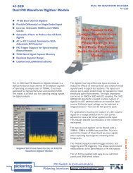
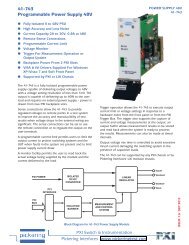
ADLINKPXI Chassis<strong>PXIS</strong>-<strong>3320</strong>15-Slot 6U PXI/CompactPCI Chassis with 500 W Hot-Swappable Power Supply1Software &Utilities2DAQIntroductionThe ADLINK <strong>PXIS</strong>-<strong>3320</strong> is a 19" 6U PXI chassis comes with one system slot and 14 peripheral slots that supports bothPXI and CompactPCI modules. Compliant with the PXI specifications Rev. 2.2, the <strong>PXIS</strong>-<strong>3320</strong> highlights a star trigger,PXI trigger bus, 10 MHz reference clock, and PXI local bus to facilitate synchronization among multiple peripheralmodules. The <strong>PXIS</strong>-<strong>3320</strong> series is equipped with two hot-swappable, industrial-grade 250 W power supply units andLEDs that tell the status of voltage, temperature, and system fans. In addition, two fan decks of <strong>PXIS</strong>-<strong>3320</strong>, which generate total482 CFM air flow, provide the ultimate thermal stability. For applications requiring multiple, multi-standard modules,and robust design, insist on ADLINK <strong>PXIS</strong>-<strong>3320</strong>.3PXI4ModularInstrumentsTHIRD PARTY PXI PRODUCTSFeatures■ Supports 6U PXI and CompactPCI modules■ PXI specifications Rev. 2.2 compliant■ Provides one system slot and 14 PXI/CompactPCIperipheral slots■ Dual hot-swappable 250 W CompactPCI power supplywith universal AC input■ Filtered, forced air-cooling architecture■ Magnetic circuit breaker protection for AC input■ Temperature, voltage, and fan monitoring LEDs■ Optional 1000 W power supplySpecificationsPower Supply■ Form factor: PICMG 2.11 compliant CompactPCIpower module■ AC input: 100 to 240 VAC, 50 Hz to 60 Hz■ DC output for each power module: 250 WVDC+5 V+12 V+3.3 V-12 VMinimum2.0 A0.0 A0.0 A0.0 ATypical25.0 A5.0 A18.0 A0.5 AMaximum33.0 A5.5 A33.0 A1.0 ACooling■ Fans for intake: Five 80 mm x 80 mm x 25 mm, dualball-bearing fans, 48.2 CFM/each■ Fans for ventilation: Five 80 mm x 80 mm x 25 mm,Storage Environment■ Ambient temperature: -20°C to 70°C■ Relative humidity: 5% to 95%, non-condensingShock and Vibration■ Shock: 15 Gpeak-to-peak, 11 ms duration■ Random Vibration• Operating: 5 Hz to 500 Hz, 0.5 G RMS, each axis• Non-operating: 5 Hz to 500 Hz, 1.88 G RMS, each axisEmissions Compliance■ EN 55022■ FCC Class ACE Compliance■ Immunity: EN 55024Recommended System ControllercPCI-6965Ordering Information<strong>PXIS</strong>-<strong>3320</strong>√■ <strong>PXIS</strong>-<strong>3320</strong>15-Slot 6U PXI/CompactPCI Chassis with500 W Hot-swappable Power Supply■ <strong>PXIS</strong>-<strong>3320</strong>/1000W15-Slot 6U PXI/CompactPCI Chassis with1000 W Hot-swappable Power Supply<strong>PXIS</strong>-<strong>3320</strong> Back View5GPIB & BusExpansion6MotionControl7Real-timeDistributedI/O8PAC9Remote I/O10Communications11dual ball-bearing fans, 48.2 CFM/eachVisionPhysical■ Number of PXI slots: 15 (1 system slot + 14 peripheral slots)■ Dimensions: 483 mm x 398 mm x 295 mm(W x H x D, without handles)■ Weight: 23 kg (50.6 lbs)Operating Environment■ Ambient temperature: 0°C to 45°C■ Relative humidity: 10% to 90%, non-condensing<strong>PXIS</strong>-<strong>3320</strong>/1000W12FanlessEmbeddedComputers13cPCI &IndustrialComputerswww.adlinktech.com 3-44
ADLINKPXI-3950/3920/39103U PXI Controllers for Hybrid PXI-based Testing SystemsPXI-3950PXI-3920PXI-3910IntroductionºTHIRD PARTY PXI PRODUCTSFeatures■ PXI specification Rev. 2.2 Compliant■ Scalable computing power• Intel ® Core2 Duo T7500 2.2 GHz processor (PXI-3950)• Intel ® Pentium ® M 760 2.0 GHz processor (PXI-3920)• Intel ® Celeron ® M 373 1.0 GHz processor (PXI-3910)■ On-board DDR2 memory• Up to 4 GB 667 MHz (PXI-3950)• 512 MB 400/533 MHz soldered (PXI- 3920/3910)■ Integrated SATA hard drive• 160 GB 7200 RPM■ CompactFlash ® socket for HDD replacement■ Integrated I/O• Dual Gigabit Ethernet ports• Four USB 2.0 ports• Built-in GPIB (IEEE488) controller• Two RS-232/422/485 ports• DVI-I video connector• High definition audio output and input• Trigger I/O for advanced PXI trigger functions■ Programmable watchdog timerThe ADLINK PXI-3900 series of PXI embedded controllers is based on the Intel® Celeron® M, Intel® Pentium® M, orIntel® Core2 Duo and specifically designed for hybrid PXI-based testing systems by providing a rugged and stable operatingenvironment for a variety test and measurement applications.Hybrid PXI-based testing systems are typically composed of a PXI platform and diversified stand-alone instruments forcomplex testing tasks. The PXI-3900 series provides plenty of interfaces, including GPIB, USB, and COM ports, forconnecting and controlling instruments. The PXI-3900 series also provides dual Gigabit Ethernet ports—one for a LANconnection and the other for controlling next-generation LXI instruments.Combining Intel® Core2 Duo T7500 2.2 GHz processor, the GME965 chipset, and 4 GB of 667 MHz DDR2 memory,the PXI-3950 provides two computing engines on a single processor that can execute two independent tasks at thesame time in a multi-tasking environment. The PXI-3920 and PXI-3910 are meticulously designed to provide maximumrobustness. The CPU and memory chips are soldered on the PCB to increase reliability in shock and vibration proneenvironments. The aluminum-copper composite heat sink helps to disperse heat uniformly to maintain a stable operatingtemperature.Combining a variety of instrument control interfaces and reliable mechanical and electronic design, the ADLINK PXI-3900series is well qualified to meet the needs of your hybrid PXI-based testing systems.■ NoticeThese PXI controllers implement rear I/O PXI controllers with rear I/O are designed to operate with a matchingrear transition module which provides internal or external chassis I/O.■ WarningIf these PXI controllers are used with a chassis that contains a rear transition module that does not match the controller, therear I/O functionality may not operate and may cause damage to the PXI controller or the rear transition module.Two COM ports,supports RS232/422/485Dual GbE ports (one forLAN connectivity andone for LXI instrumentcontrol)Four USB 2.0 ports forperipheral devices andUSB instrument controlTrigger I/O to routetrigger to/from PXItrigger busDVI-I connector for DVI(digital) or CRT (analog)displayMicro-D GPIB connectorfor GPIB instrumentcontrolHigh definition audioline-in and speaker outPXI-3950 Front Panel3-5 www.adlinktech.com6
ADLINK1Software &Utilities2DAQSpecificationsCore FeaturesCPUFSBChipsetMemoryModel Name PXI-3910 PXI-3920 PXI-3950DisplayChipsetDVICRTLVDS (For rear I/O only)InterfaceI/O ConnectivityHard DriveEthernetUSBGPIBSerial PortAudioTrigger I/OCompactFlash SocketMechanical and EnvironmentalDimensionsSlot RequirementsWeightOperating Temp.Storage Temp.Relative HumidityShockVibrationEmissions ComplianceCE ComplianceIntel ® Celeron ® M 373 1.0 GHz Intel ® Pentium ® M 760 2.0 GHz Intel ® Core2 Duo T7500 2.2 GHz400 MHz 533 MHz 800 MHzIntel ® 915 GME Graphic Memory Control HUBIntel ® GME965 Graphic Memory Control HUBIntel ® I/O Controller Hub 6 Mobile (ICH6-M)Intel ® I/O Controller Hub 8 Mobile (ICH8-M)512 MB on-board soldered memory 4 GB SO-DIMM memoryOne DDR2 SO-DIMM socket for memory expansionSupports dual-channel DDR2 SDRAM, 667 MHzSupports dual-channel DDR2 SDRAM, 400/533 MHzIntel ® GMA 900 graphic media acceleratorSingle channel TMDS via SDVO to DVI controller up to 1600 x 1200 resolution @ 60 HzAnalog CRT route to DVI-I connector on the faceplate up to 1280 x 1024 resolutionSingle 18-bit LVDS channel route to rear transition moduleSupports LCD backlight controlDVI-I connector for digital or analog video signal outputs160 GB SATA hard drive, 7200 RPMOn board Marvell 88E8053 Dual Gigabit Ethernet controllersTwo RJ-45 connectors with speed/link/active LED on the faceplate4 x USB 2.0 on the faceplateOn-board IEEE488 GPIB controllerMicro-D 25-pin connector on the faceplate (ACL-IEEE488-MD1 cable required)Two 16C550 UART compatible COM ports on the faceplateSupports RS-232, RS-422, and RS-485, configurable by jumper settingSupports high definition audio input/outputTwo audio jacks on the faceplate for line-in/mic-in and speaker-outSMB connector on the faceplate to route an external trigger signal to/from PXI trigger busType II CF Socket, supporting PIO and DMA modes3U PXI module 60.5 mm x 128.7 mm x 213.2 mm1 system slot plus 2 controller expansion slots0.9 kg0 to 55°C-20 to 80°C5 to 95%, non-condensing30 G, half-sine, 11 ms pulse durationOperating: 5 to 500 Hz, 0.5 GRMS, 3 axesNon-operating: 5 to 500 Hz, 2.46 GRMS, 3 axesEN 61326-1FCC Class AImmunity: EN 61326-1Intel ® GMA X3100 graphic media accelerator3PXI4ModularInstruments5GPIB & BusExpansionTHIRD PARTY PXI PRODUCTS6MotionControl7Real-timeDistributedI/O8PAC9Remote I/O10Ordering InformationCable AccessoryCommunications■ PXI-39503U PXI Core2 Duo T7500 2.2 GHz SystemController with 4 GB Memory & 160 GB HDD■ PXI-39103U PXI Celeron ® M 373 1.0 GHz System Controllerwith 512 MB memory & 160 GB HDD11■ PXI-3950/M2G3U PXI Core2 Duo T7500 2.2 GHz SystemController with 2 GB Memory & 160 GB HDD■ PXI-39203U PXI Pentium ® M 760 2.0 GHz SystemController with 512 MB Memory & 160 GB HDD■ PXI-3920/M1.5G3U PXI Pentium ® M 760 2.0 GHz SystemController with 1.5 GB Memory & 160 GB HDD■ ACL-IEEE488-MD125-pin Micro-D to GPIB Cable, 1 Meter LengthVision12FanlessEmbeddedComputers13cPCI &IndustrialComputerswww.adlinktech.com 3-67
ADLINKTerminal Boards & Cables■ DIN-37D-01Terminal Board with One 37-pin D-sub Connectorand DIN-Rail Mounting (Cables are not included.)■ ACLD-9137-01General-Purpose Terminal Board with One 37-pinD-sub Male Connector■ ACLD-9137F-01General-Purpose Terminal Board with One 37-pinD-sub female Connector.■ ACL-10137-1MM37-pin D-sub male/male cable, 1 M■ ACL-10137-1MF37-pin D-sub male/female cable, 1 M* For more information about mating cables, please refer toP2-59/60.Note: A rear I/O terminal board (cPCI-R6216DB) has beenincluded with the cPCI-6208V/R-GL, cPCI-6216V/R-GL andcPCI- 6208A/R. This cPCI-R6216DB rear I/O board is responsiblefor conducting I/O signals from the CompactPCI J2 connectorto a 37-pin D-sub connector.Ordering Information■ PCI-6208V-GL8-CH 16-Bit Voltage Output Card■ PCI-6216V-GL16-CH 16-Bit Voltage Output Card■ PCI-6208A8-CH 16-Bit Voltage and Current Output Card■ cPCI-6208V-GL8-CH 16-Bit Voltage Output Module■ cPCI-6208V/R-GL8-CH 16-Bit Voltage Output Module with Rear I/O■ cPCI-6208A8-CH 16-Bit Voltage and Current Output ModulePin AssignmentPCI/PCIe/cPCI-6208V-GL andPCI/PCIe/cPCI-6216V-GLDI3DI2DI1DI0GND+5Vout+15VoutAGNDNC/V14V6AGNDNC/V12V4AGNDNC/V10V2AGNDNC/V8V012345678910111213141516171819202122232425262728293031323334353637(PCI/cPCI-6208A)DI3DI2DI1DI0GND+5Vout+15VoutAGNDA6V6AGNDA4V4AGNDA2V2AGNDA0V012345678910111213141516171819202122232425262728293031323334353637DO3DO2DO1DO0GND-15VoutAGNDNC/V15V7AGNDNC/V13V5AGNDNC/V11V3AGNDNC/V9V1DO3DO2DO1DO0GND-15VoutAGNDA7V7AGNDA5V5AGNDA3V3AGNDA1V1THIRD PARTY PXI PRODUCTS■ cPCI-6208AR8-CH 16-Bit Voltage and Current Output Modulewith Rear I/O■ cPCI-6216V-GL16-CH 16-Bit Voltage Output Module■ cPCI-6216V/R-GL16-CH 16-Bit Voltage Output Module with Rear I/O■ PCIe-6208V-GL8-CH 16-Bit Voltage Output PCI Express ® Card■ PCIe-6216V-GL16-CH 16-Bit Voltage Output PCI Express ® CardNote: Rear I/O versions can not be used in PXI chassis due tosignals conflict with PXI bus.9w
AGILENTSpecifications and CharacteristicsHardware M9182A M9183AcontinuedOther measurements n/a Offset compensatedohms, pulse width &duty cycle, totalizer/event counterDC Source n/a ± 10 V, ± 12 mAFloating isolation 300 Vrms 300 Vrms(Cat-II)ConnectorcPCI, PXI-H, PXI-1compatibilitySensitivityFunction Lowest Range SensitivityDCV 200.0000 mV 0.1 µVACV 200.0000 mV 0.1 µVResistance (M9183A) 20.00000 Ω 10 µΩResistance (M9182A) 200.0000 Ω 100 µΩDCI (M9183A) 200.0000 nA 0.1 pADCI (M9182A) 2.000000 mA 10 nAACI 2.000000 mA 1 nACapacitance 1000.0 pF 0.1 pFResolution vs. aperture and reading rate for DCV, DCI, ΩMeasurementapertureSoftwareSoftwaredevelopmentplatformIncluded GUIApplication codeexamplesMaximumreadings persecondResolution10 ms 98 6½ digits (22 bits)625 µs 1,200 5½ digits (18 bits)130 µs 4,500 4½ digits (14 bits)2.5 µs(M9183A only)System requirementsOperating systems15,000 4½ digits (14 bits)Microsoft Windows ® XP,Microsoft Windows ® Vista (32/64 bit),Microsoft Windows ® 7 (32/64 bit)Visual Studio ® (VB.NET, C#, C/C++),LabVIEW, LabWindows/CVI, VEE,MATLABSoft front panelC/C++ ® , Visual Basic ®Soft Front PanelAgilent soft front panel provides easy to use instrumentcontrol. The M9182A and M9183A graphical user interfaceguides developers through module setup so users canquickly configure the DMM.Ordering InformationModelM9182AM9183AAccessories34138ADescriptionPXI Digital Multimeter-6½ DigitPXI Digital Multimeter-6½ Digit,Enhanced PerformanceTest Lead SetDiscover Agilent ....www.agilent.comwww.agilent.com/find/modularlarwww.agilent.com/find/pxi-dmmUSA: (800) 829-4444PXI is a registered trademark of the PXI Systems Alliance.Visual Basic, C++, Windows, and MS Windows are U.S.registered trademarks of Microsoft Corporation.For more information on Agilent Technologies’ products, applications, orservices, please contact your local Agilent office. The complete list isavailable at: www.agilent.com/find/contactusProduct specifications and descriptions in this document subject to changewithout notice.© Agilent Technologies, Inc. 2011 Printed in USA, April 25, 20115990-6550ENTHIRD PARTY PXI PRODUCTS11
APPLICOSPXI Dual channel 24-bit / 192ksps AWGBlock diagramData BusDATA BUFFER100kHzP X I B U S I N T E R F A C EChannel-A memoryPX I S TARPX I T R IG 0PX I T R IG 5Channel-B memoryad dre ss c oun teren d add res ss ta rt a ddr es ss ta rt a ddr es sen d add res sad dre ss c oun terData BusC LO C KLO G ICT R IG G ERLO G ICDATA BUFFERSpecifications (conditions: T A=25ºC)24 bitSigma-DeltaDAC73MHzINTERNALCLOCK45MHzINTERNALCLOCK24 bitSigma-DeltaDACGeneralChannels 2Resolution24-bitUpdate rate, internal clock 3.675ksps - 192kspsUpdate rate, external clock 1ksps - 220kspsMemory depth1M-word per channelOutput range10mV to 10Vpp continuousOutput configurationSingle ended or differentialOutput impedance600-Ω or low impedanceAnalog filters (low pass) 100kHz, 22kHz or 1.2kHzOutput operating area -10V to +10VAccuracyAmplitude accuracy±0.05dB @ 1kHz/10VppFrequency flatness0.2dB from 20Hz to 20kHzATTEN-UATORATTEN-UATOR22kHz1.2kHz100kHz22kHz1.2kHzDACDC-OFFSETDAC-ADACDC-OFFSETDAC-BDifferentialoutput stageDifferentialoutput stage600600600600OUT A +OUT A -EXTERNALCLOCK-INEXTERNALTRIGGER-INOUT B +OUT B -Dynamic characteristics(Vout = 10Vpp, f-upd.=192ksps)SINAD (1kHz)107dB (BW=20kHz)SFDR (1kHz)112dBTHD (1kHz)110dBTHD (1kHz with 1.2kHz filter) 125dB (typical)THD (10kHz)103dBCommon mode voltage sourceVoltage range-5V to +5V.Resolution16-bit (152µV)Clock & Trigger inputsClock Input50-Ω, V IL1.4VTrigger input10kΩ, V IL2.0VTriggeringTrigger sourcesSoftware, External, PXI STAR,PXI TRIG 0..7Trigger capabilitiesedge or level, positive or negativegoing. Independent trigger sourceselection per channelTHIRD PARTY PXI PRODUCTSDocument revision 2.0Applicos || Veldkampseweg 1 || 8181LN Heerde || The Netherlands || Tel: +31 578 696769 || www.applicos.com13
APPLICOSPA72 Series - PXI Generator & Digitizer platformTHIRD PARTY PXI PRODUCTSFeatures Flexible analog signal generation andcapture platform Two daughter board slots On-board high performance clocksource On-board high accuracy voltmeter Hybrid slot compatible 1ppm clock stability / 0.5ps clock jitterThe PA72 is a PXI base board designed to carry one or two highperformance analog daughter boards. The main board containsall common hardware like; clock source, trigger circuitry, businterface, supply regulation and a high precision voltmeter. Thedaughter boards determine the actual analog performance. ThePA72 concept provides a flexible and cost effective solution formedium and high end analog functions.The two daughter board slots can contain one of the availableGenerator or Digitizer boards listed on page 3. Also customdaughter boards can easily be created.User control panel for the PA72 and an AWG daughter boardThe PLL clock source is capable of generating any frequencybetween 2kHz up to 945MHz. This allows a wide range ofdaughter boards to be supported. The frequency stability isbetter than 1ppm and the jitter only 0.5ps. The frequency canbe locked to the PXI backplane 10MHz or an external clock.The on-board high accuracy voltmeter is used for automaticcalibration. Most daughter boards also support measuringexternal DC voltages.The PA72 uses the 32-bit PXI bus and supports burst mode. Thisallows up to 132MByte data throughput. The J2 con-nector is asmall version to make it hybrid slot compatible.14
APPLICOSPA72 Series - PXI Generator & Digitizer platformBlock DiagramDescription:The PA72 base board contains a clock generator, triggercircuitry, a digital voltmeter and the PXI bus interface. In theabove diagram the base board functions are yellow and thedaughter board functions are green.The clock generator is a low jitter PLL clock that has less than0.5ps jitter for low loop filter bandwidths. With higher loop filterbandwidths, frequency settling time can be less than 250ms.The main clock frequency ranges from 2kHz up to 945MHz witha resolution of less than 1 kHz. Each daughter boardslot has its own divider. Therefore the clock for each daughterboard can be different while maintaining propersynchronization. The PLL clock generator features a high stabilitylow noise and low jitter 10MHz on-board reference clock with1ppm frequency stability. In addition the PLL can be locked tothe PXI backplane clock or to an external reference clock. Alsocan the on-board clock source be bypassed by an external clock.The trigger input supports edge and level triggering and positiveand negative going trigger signals. The trigger source can besoftware, PXI-Star, PXI 0-7 or external.THIRD PARTY PXI PRODUCTSSpecifications PA72 main board:PLL clockFrequency range 2kHz to 945MHzSync possibilities 10MHz backplane or 10MHz external clockPLL lock time 250ms - 1s (depending on loop filter BW)Jitter0.5ps typicalExternal clock inputClock rate DC to 500MHzTreshold level 0V or 1V (programmable)Input impedance 50-OhmTrigger inputTreshold level 1VInput impedance 1k OhmMax input level -0.5V to +5.5VCoupling DCTrigger sourcesExternal, PXI STAR, PXI TRIG 0..7, Software triggerEach trigger can be programmed to be edge or level and positiveor negative going. Independent trigger source selection perchannelApplicos || Veldkampseweg 1 || 8181LN Heerde || The Netherlands || Tel: +31 578 696769 || www.applicos.com15
APPLICOSPA72 Series - PXI Generator & Digitizer platformBrief specifications of available daughter boards (see individual daughter board product sheet for more information)THIRD PARTY PXI PRODUCTSPA72G16400, 16-bit / 400Msps AWGChannels 1Resolution16-bitUpdate rate with PA72 clock 2kHz to 400MHzUpdate rate external clock DC to 400MHzPattern depth8M-wordsOutput ranges Single ended 0.32Vp to 2.56Vp in 6 rangesOutput ranges Differential 0.64Vp to 5.12Vp in 6 rangesOutput offset voltage-2.56 to +2.56V (16-bit resolution)Output configuration50-Ohm, Single Ended or DifferentialOutput filtersNone, 60MHz, 30MHzAbsolute accuracy(500V+0.08% of range)Relative accuracy0.003%SNR (200Msps, 2.5Vp diff.) 70dB @ f-out = 1MHz (BW: 0-80MHz)SNR (200Msps, 2.5Vp diff.) 67dB @ f-out = 10MHz, (BW: 0-80MHz)THD (200Msps, 2.5Vp diff.) 87dB @ f-out = 1MHzTHD (200Msps, 2.5Vp diff.) 80dB @ f-out = 10MHzSFDR (200Msps, 2.5Vp diff.) 85dB @ f-out = 1MHzPA72G14150, 14-bit / 150Msps AWG (Preliminary)Channels 1Resolution14-bitUpdate rate with PA72 clock 2kHz to 150MHzUpdate rate with ext. clock DC to 150MHzPattern depth64M-wordsOutput configuration50-Ohm, Single ended or DifferentialOutput ranges0.228Vp to 2.56Vp in 8 rangesOutput filtersNone, 30MHz, 15MHzDC-offset voltage-2.56V to +2.56VAbsolute accuracy(750V+0.1% of range)Relative accuracy (INL) ±0.025% of rangeSNR (150Msps, 2.0Vp diff.) 69dB @ f-out = 1MHz (BW: 0-70MHz)SNR (150Msps, 2.0Vp diff.) 64dB @ f-out = 10MHz, (BW: 0-70MHz)THD (150Msps, 2.0Vp diff.) 74dB @ f-out = 1MHzTHD (150Msps, 2.0Vp diff.) 70dB @ f-out = 10MHzSFDR (150Msps, 2.0Vp diff.) 78dB @ f-out = 1MHzPA72D16180, 16-bit / 180Msps DigitizerChannels 1Resolution16-bitSample rate (PA72 and ext.) 1MHz to 180MHzMemory depth64M-wordsInput ranges0.256Vp to 3.072Vp in 8 rangesInput configurations50-Ohm, AC or DC, Diff.or Single EndedDC-offset voltage the input range (16-bit resolution)Input bandwidth≥80MHzInput filtersNone, 60MHz, 30MHzAbsolute accuracy(800V+0.1% of range)Relative accuracy0.006%SNR (160Msps, 2Vp diff) 70dB @ f-in = 1MHz (BW: 0-80MHz)SNR (160Msps, 2Vp diff) 68dB @ f-in = 10MHz (BW: 0-80MHz)THD (160Msps, 2Vp diff) 87dB @ f-in = 1MHzTHD (160Msps, 2Vp diff) 81dB @ f-in = 10MHzSFDR (160Msps, 2Vp diff) 83dB @ f-in = 1MHzPA72D14130, 14-bit / 130Msps Digitizer (Preliminary)Resolution14-bitSample rate1MHz - 130MHzMemory depth64M-wordInput configurationDifferential or single endedInput ranges (span)0.338Vp to 3.6Vp in 8 rangesDC-offset voltage-2.56V to +2.56VInput operating area-3.6V to +3.6VInput impedance10kOhm, 50-Ohm DC or 50-Ohm ACInput filtersNone, 30MHz, 15MHzAbsolute accuracy(750V+0.1% of range)Relative accuracy (INL) ±0.025% of rangeSNR (120Msps, 2.0Vp diff.) 68dB @ f-out = 1MHz (BW: 0-60MHz)SNR (120Msps, 2.0Vp diff.) 64dB @ f-out = 10MHz, (BW: 0-60MHz)THD (120Msps, 2.0Vp diff.) 75dB @ f-out = 1MHzTHD (120Msps, 2.0Vp diff.) 71dB @ f-out = 10MHzSFDR (120Msps, 2.0Vp diff.) 77dB @ f-out = 1MHzModule numbering:The configuration of a PA72 module is determined as follows:PA72-nmn = daughter board 1 (top position)m = daughter board 2 (bottom position)Daughter board codes:0 = empty1 = PA72G164002 = PA72G141505 = PA72D161806 = PA72D14130For example a PA72-15 is a PA72 base board with a 16-bit / 400Msps AWG in the top position and a 16-bit / 180Msps Digitizer in the bottom positionDocument revision 1.1Applicos || Veldkampseweg 1 || 8181LN Heerde || The Netherlands || Tel: +31 578 696769 || www.applicos.com16
APPLICOSPXI Dual channel 24-bit / 192ksps DigitizerPD24222 Two channels, fully differential inputs Excellent dynamic performance 114dB THD typical at 1kHz / 96ksps Programmable DC-offset level 31.6mVpp to 10Vpp output range 1MΩ or 600-Ω input impedance Internal clock supports all standard audio rates Local bus clock for sync. to PG24192The PD24222 is a PXI, Dual Channel Digitizer. Itfeatures fully differential inputs and a very lowdistortion. For differential measurements the inputsignals may have any common mode level as longas the common mode level plus signal stay within the-10V to +10V range. Alternatively AC coupling can beused. For single ended applications the PD24222has a programmable DC offset source that can beconnected to the negative input. This ensures the fullresolution of the converter can be maintained whencapturing signals with a DC offset.The unit is very suitable for audio type ofmeasurements. The flexible input ranging andcoupling allow easy adaptation to a wide range ofUnit Under Test output voltages.The two channels are ideal for stereo and phase shiftmeasurements. The selectable 22kHz or 100kHz lowpass filters reduce the out of band noise.The internal clock sources can generate all standardaudio sample rates and more. The External clockand trigger capability give the user full control of themeasurement timing. If the PG24192 is used asgenerator, the clocks of the two units can besynchronized via the local bus capability of the PXIbackplane. This allows coherent clocking for bestmeasurement results.THIRD PARTY PXI PRODUCTSDC to 48kHz spectrum, 1kHz carrier, 96ksps.17
APPLICOSPXI Dual channel 24-bit / 192ksps DigitizerBlock diagramTHIRD PARTY PXI PRODUCTSIN A(+)IN A(-)EXTERNAL CLOCK (in)TRIGGERIN B(+)IN B(-)600OhmDAC600OhmDACDifferential tosingle endedrangable amplifier- input +input- input +inputDC-OFFSETDAC CH-A (16 bit)Differential tosingle endedrangable amplifierDC-OFFSETDAC CH-B (16 bit)Specifications (conditions: T A =25ºC)100kHz LPF22kHz LPF100kHz LPF22kHz LPFGeneralChannels 2Resolution24-bitSample rate, internal clock 5ksps - 192kspsSample rate, external clock 1ksps - 220kspsMemory depth1M-word per channelInput range31.6mV to 10Vpp in 10dB stepsInput configurationSingle ended or differentialInput couplingAC or DCInput impedance 1MΩ or 600-ΩInput operating area -10V to +10VAnalog filters (low pass) 100kHz, 22kHzAccuracyAmplitude accuracy±0.05dB@ 1kHz/10VppFrequency flatness0.2dB from 20Hz to 20kHz24 bit ADC24 bit ADCDATA BUFFER73MHzINTERNALCLOCK45MHzINTERNALCLOCKDATA BUFFERData Busa d d r e ss c o u n te rC LO C KLO G ICe n d a d d r e ssT R IG G ERLO G ICe n d a d d r e ssa d d r e ss c o u n te rData BusCH-B capture memory CH-A capture memoryPX I C L K 10PX I S TARPX I T R IG 0PX I T R IG 7Dynamic characteristics(Vin = 9Vpp, f-sample.=192ksps)SINAD (1kHz)103dB (BW=20kHz)SFDR (1kHz)110dBTHD (1kHz)105dBTHD (1kHz@96ksps, typical) 114dBTHD (10kHz)103dBDC-offset voltage sourceVoltage range-5V to +5V.Resolution16-bit (152µV)Clock & Trigger inputsClock Input50-Ω, V IL1.4VTrigger input10kΩ, V IL2.0VTriggeringTrigger sourcesSoftware, External, PXI STAR, PXITRIG 0..7Trigger capabilitiesedge or level, positive or negativegoing. Independent trigger sourceselection per channelP X I B U S I N T E R F A C EDocument revision 2.01Applicos || Veldkampseweg 1 || 8181LN Heerde || The Netherlands || Tel: +31 578 696769 || www.applicos.com18
BALLARDLC429-3ARINC 429 Interfacefor CompactPCI ComputersFeaturesUp to eight ARINC channelsFor rugged, industrial applicationsAutomatic speed detection onreceive channelsError injection and detectionExtensive monitoring capabilityCoPilot 429 and CoPilot 429Plus graphical software availableEasy plug-and-play CompactPCIinterfaceUpgrade later as requirementschangeOptional ARINC 717 Flight DataRecorder interfaceDescriptionThe LC429-3 is a flexible, powerfulARINC 429 avionics databusinterface board for the developmentand maintenance of commercialavionics. Installed in aCompactPCI® computer, userscan transmit and receive messageson up to eight databuses. Severalmixes of transmit and receivechannels are available, and unitscan be upgraded at any time tomeet changing requirements. Theadvanced features, ease-of-use,and upgrade paths make theLC429-3 an ideal solution forARINC 429 hardware and systemdevelopment, testing, and simulation.The LC429-3 can be easily configuredto automatically transmitand receive labels (ARINC 429words) while saving a sequentialrecord of the activity of interest. Atany time, the host computer canwrite or read data, alter transmitlabels, or read receive labels withoutinterfering with the operationof the LC429-3. Transmissions areautomatically maintained at thespecified transmit intervals andmay include concurrent aperiodiclabels for file data transfer protocols.Received data are filtered bylabel/SDI and saved according touser specifications. The sequentialrecord is a time-tagged history ofdatabus activity that can be savedfor later analysis. The user specifieswhich labels go in the sequentialrecord and what otherperformance information is to berecorded.HardwareOnce configured, the LC429-3hardware can transmit, receive,and build the sequential recordwithout requiring any processingby the host computer. The onboard,high-speed DSP, largememory, and custom gate arraysprovide power and flexibility forTHIRD PARTY PXI PRODUCTS11400 Airport Road, Everett, WA 98204-8782 USA Tel: (800) 829-1553 (425) 339-0281 Fax: (425) 339-0915E-mail: sales@ballardtech.com Web: www.ballardtech.com19
BALLARDTHIRD PARTY PXI PRODUCTS20the multitude of LC429-3 featuresand user options. An interface tothe ARINC 717 Flight Data Recorderdatabus is available as an option.SoftwareThe easiest way to use theLC429-3 is with Ballard’s CoPilot429 graphical software (availablewith board or separately). Usingthe ARINC 429 database of equipmentIDs and label definitions, userscan quickly build transmitschedules and display data inmeaningful engineering units. Thepowerful Sequential Monitor capturesdata and saves time-taggedmessages to a host file for subsequentprocessing and analysis. Inaddition, CoPilot 429 Plus providesvirtual instruments, strip charts,and moving map displays, as well asscripting routines and hardwareand software playback.The LC429-3 comes bundledwith an Application Program Interface(API) which enables quick andeasy development of solutions.The LC429-3 can be configured forsimple applications with only a fewAPI calls using default options. Al-11400 Airport RoadEverett, WA 98204-8782 USATel: (800) 829-1553 (425) 339-0281Fax: (425) 339-0915E-mail: sales@ballardtech.comWeb: www.ballardtech.comthough most users will accomplishtheir tasks with a small number ofAPI functions, the comprehensivelibrary includes a broad range oftools for specialized needs. Alsoprovided are many example programswith source code.Driver software is included forWindows® 95/98/NT/Me/2000/XP and LabVIEW®. Linux andVxWorks® drivers are available.Ordering InformationLC429-3/xRyT: ARINC 429Interface Card (where x is the numberof receive channels and y is thenumber of transmit channels). Thenine standard combinations are asfollows:Total ChannelsxRyT Combinations2 1R1T4 4R0T 2R2T 0R4T8 8R0T 6R2T 4R4T2R6T 0R8TIncludes circuit board, API library,and manual.Cz-LC43/xRyT: CoPilot 429System (z is S for CoPilot standardand P for CoPilot Plus). Includesthe LC429-3 (options specified asabove) and CoPilot 429 software.Specializing in avionics databusesMIL-STD-1553ARINC 429/575/629/708/717SPACE SHUTTLECustom ProductsTechnical Specifications:LC429-3Number of Channels2, 4, or 8 in nine standard configurationsTransmit ChannelsSpeedLow (12.5 Kbps)High (100 Kbps)Software-established schedulePeriodic and/or file transferContinuous cycle or single wordInternal or external triggerError generationParity, word gap (0 to 3 bit times)Receive ChannelsSpeedAuto-detect or fixedLow (12.5 Kbps)High (100 Kbps)FiltersWords mapped by filter valueUp to 1024 label/SDIs per channelError detectionMinimum gap, bit count, bitencoding, parityTime-tag, selectable range/resolutionSequential RecordTime-tagged recording of user selectedmessagesInterval and Delta modes for samplingand record compressionDSP Core80 MHz Digital Signal ProcessorMemory1 MB SRAM32 KB true dual-port RAMUser-configurable list buffersInterruptsSoftware-configurable interrupt log listGenerated on user-specified conditionsScheduleErrorsSpecific messagesCompactPCI Interface32 bits at 33 MHz3U x 4HP card (100 x 160 mm)Plug-and-playFor 5 Volt cPCI backplaneConnector25-pin male D-subOther signalsExternal TriggerSync OutputDigital I/O (4)Temperature gradescommercial (std)extended temperature availableSoftwareEasy-to-use APIIncluded drivers: Windows 95/98/NT/Me/2000/XP and LabVIEWAvailable drivers: Linux and VxWorksOptional CoPilot 429 and CoPilot 429Plus softwareWindows® 95/98/NTMe/2000/XP are registeredtrademarks of Microsoft Corp. CompactPCI® is aregistered trademark of the PCI Industrial ComputerManufacturers Group, Inc. LabVIEW® is aregistered trademark of National InstrumentsCorp. VxWorks® is a registered trademark ofWind River Systems, Inc.BR129-20081030
BALLARDLC1553-3 A, B, and CMIL-STD-1553 Interfacefor CompactPCI ComputersFeaturesSingle/multiple terminalsFor use in rugged, industrialapplicationsConcurrent Bus Controller,Remote Terminal, and MonitorExtensive monitoring capabilityError injectionProgrammable 32-bit time-stampAPI and driver software includedCoPilot 1553 and CoPilot 1553Plus graphical software availableEasy plug-and-play CompactPCIinterfaceA Family of ProductsChoose functionality suited toimmediate needsUpgrade later as requirementschangeOngoing release of features andproductsSelect from several standardconfigurations and a variety ofoptionsCan be customized for specialneedsExceptional valueDescriptionThe LC1553-3x is a family ofdual-redundant MIL-STD-1553 interfaceboards for CompactPCI®computers. This family of productsprovides a range of capabilitiesfrom basic, single-terminal emulationto multi-terminal simulation anderror injection. Models can be upgradedin the future to meetchanging requirements. The pow-erful features and upgrade pathsmake the LC1553-3 an ideal solutionfor hardware and systemdevelopment, testing, and simulation.HardwareAll models provide Bus Controller,Remote Terminal, and Monitoroperation and support all 1553message types. Advanced modelscan simultaneously operate as theBus Controller, Monitor, any numberof Remote Terminals, andselectively inject protocol errors.The powerful DSP core of theLC1553-3 offloads 1553 protocolprocessing from the host PC. Thelarge, on-board memory and flexiblemessage buffering schemesensure data integrity. Polling andinterrupt generation are simplifiedthrough a generous set of useroptions.SoftwareThe easiest way to use theLP1553-3 is with Ballard’s CoPilot1553 graphical software (availablewith board or separately). Usingthe automation and detection toolsin CoPilot, users can create andrun BC schedules, simulate RTs,THIRD PARTY PXI PRODUCTS11400 Airport Road, Everett, WA 98204-8782 USA Tel: (800) 829-1553 (425) 339-0281 Fax: (425) 339-0915E-mail: sales@ballardtech.com Web: www.ballardtech.com21
BALLARDTHIRD PARTY PXI PRODUCTS22and monitor the bus with just a fewclicks of the mouse. Users canview and edit data in engineeringunits through specialized displays.In addition, CoPilot 1553 Plus providesvirtual instruments, stripcharts, and moving map displays,as well as scripting routines andsoftware playback.Alternatively, software developerscan use the bundledApplication Program Interface(API) that enables quick and easydevelopment of custom applications.The LC1553-3 can beconfigured for simple terminalemulation using default memorymapping and buffering options withonly a few API calls. Although mostusers will accomplish their tasksLC1553-3 Product HighlightsFeatures11400 Airport RoadEverett, WA 98204-8782 USATel: (800) 829-1553 (425) 339-0281Fax: (425) 339-0915E-mail: sales@ballardtech.comWeb: www.ballardtech.comwith a small number of API functions,the omprehensive libraryincludes a broad range of tools forspecialized needs.Driver software is included forWindows® 95/98/NT/Me/2000/XP and LabVIEW®. Linux andVxWorks® drivers are availableseparately.Ordering InformationLC1553-3x: MIL-STD-1553 InterfaceCard (where x is A, B4, B32or C; see table below). Includesboard, API library, and manual.Cy-LC13x: CoPilot 1553 System(y is S for CoPilot standard and P forCoPilot Plus). Includes the LC1553-3 card as described above andCoPilot 1553 software.ModelsA B4 B32 CNumber of simultaneous terminals 1 4 32 32Monitor Filtering for terminal addresses Filtering for subaddresses Concurrent with terminal simulationError InjectionOn-board RAM 256K 256K 256K 1MBSpecializing in avionics databusesMIL-STD-1553ARINC 429/575/629/708/717SPACE SHUTTLECustom ProductsTechnical Specifications:LC1553-3ModesBus ControllerOn-board message frame timingTransmission retriesException processingRemote TerminalIllegalize subaddress/mode codesInterrupt on message or terminalaccessMonitorSnapshot or sequentialFiltering on terminal and/or SAIndependent or concurrentwith BC/RTHandles all 1553A/B message typesNotice 2–selectable featuresMessage Bufferingsingleping-pongcircular list (transmit only)FIFO listMulti-terminal simulation (B, C models)Error generation (C model only)Types:SyncParityManchesterBit countWord countInject into specific bits/words/messagesDSP coreMemory256K standard1MB optional (standard on C model)High-performance interfaceInterruptsSoftware-configurable interrupt log listGenerated on user-specified conditionsScheduleErrorsSpecific messagesTime-tagAutomatic in all modes32-bit, selectable range/resolutionCompactPCI Interface32 bits at 33 MHz3U x 4HP card (100 x 160 mm)Plug-and-playFor 5 Volt cPCI backplaneConnectorsTwinax BJ77 mates with PL75Other signalsExternal TriggerSync OutputDigital I/OTemperature Gradescommercial (std)extended temperature availableSoftwareEasy-to-learn APIIncluided drivers: Windows 95/98/NT/Me/2000/XP and LabVIEWAvailable drivers: Linux and VxWorksCustomized firmware availableOptional CoPilot 1553 and CoPilot1553 Plus softwareWindows ® 95/98/NT/Me/2000/XP are registered trademarksof Microsoft Corp. LabVIEW ® is a registeredtrademark of National Instruments Corp. VxWorks ® is aregistered trademark of Wind River Systems, Inc.BR130-20081030
EKFProduct InformationCCM-BOOGIE • Core 2 Duo CompactPCI ® CPUHigh Performance Dual Core ProcessorDual Screen Video • Dual Gigabit Ethernet • Dual Channel Memory • 6 x SATA RAIDThe CCM-BOOGIE is a versatile 4HP/3UCompactPCI ® CPU board, equipped with anIntel® Core 2 Duo processor at up to2.26GHz clock, and up to 6GB dual channelcapable DDR3 RAM. Four native 3Gbps RAIDcapable Serial ATA channels are available formass storage I/O, and in addition another twofrom a secondary RAID controller. TheCCM-BOOGIE has been designed especially forsystems which require dual core highperformance at moderate power consumption.Document No. 5198 • 23 August 2011The CCM-BOOGIE is provided with a highperformance mobile chipset (Intel® GS45)which operates at up to 1066MHz FSB and upto 1066MHz DDR3 memory clock for optimumsystem throughput. The chipset is based on PCIExpress® technology and has a powerfulintegrated graphics accelerator. The DVI-I frontpanel connector enables dual screen videooperation. Two Gigabit Ethernet controllers areprovided for high speed connectivity (one ofthem IEEE 802.1as TimeSync compliant).THIRD PARTY PXI PRODUCTSCCM-BOOGIE with SATA SSD23
EKFCCM-BOOGIE • High Performance Dual Core CompactPCI ® CPUThe CCM-BOOGIE is equipped wit a set of localexpansion interface connectors, which can beoptionally used to directly attach a suitable(application specific) mezzanine side board, e.g.for audio- and legacy support, PCI Expressbased I/O circuitry, and a secondary DVI videooutput. Carrier board and side card come as areadily assembled 8HP unit typically. Mostmezzanine cards can accommodate in additiona 2.5-inch drive. Also as an option, a suitablerear I/O transition module is available to theCCM-BOOGIE.As a popular add-on option, the CCM-BOOGIEcan be delivered with a small mezzaninemodule (C42-SATA), which accommodates a1.8-inch SATA solid state drive (SSD).Alternatively, the C40-SCFA mezzanine card isprovided with an industrial grade CompactFlashmemory card, and/or an even more rugged USBSilicon State Drive (SSD). In addition, theC41-CFAST is available, equipped with a CFastcard socket. Any of the C41...C43 mezzaninemodules fits into the 4HP envelope of the entireassembly.THIRD PARTY PXI PRODUCTSBenefits of the CCM-BOOGIE< High Performance CompactPCI® System Slot Controller with or w/o Rear I/O< Hybrid Systems Option 1 (Dual Backplane CompactPCI® & CompactPCI® Serial)< Hybrid Systems Option 2 (Dual Backplane CompactPCI® & CompactPCI® Express)< Intel® Core 2 Duo SV (45nm Penryn) Mobile Processor 2.26GHz 6MB L2 Cache (FSB1066MHz)< Scalable Series of Small Form Factor (SFF) Processors from 1.2GHz to 2.26GHz< Cool Operation by Means of ACPI UEFI BIOS< PCI Express Mobile Intel® 45 Express Chipset GS45 (Cantiga)< Up to 6GB DDR3 Memory (Dual Channel Mode Capable, up to 1066MHz)< One Memory Bank Soldered (Low Memory) for Extreme Ruggedized Systems< Dual-Screen Graphics Controller< Dual Gigabit Ethernet Controllers< Four Native SATA Channels 3Gbps, Intel® Matrix Raid Storage Technology< Two Additional SATA Channels 3Gbps, RAID capable with JMicron Drivers< Eleven USB 2.0 channels< SATA 1.8-Inch Solid State Drive (SSD) with C42-SATA Mezzanine Module Option (4HPMaintained)< CFast Card and/or USB SSD with C41-CFAST Mezzanine Module Option (4HPMaintained)< CompactFlash and/or USB SSD with C40-SCFA Mezzanine Module Option (4HPMaintained)< Variety of Mezzanine Expansion Boards Available with and w/o PCIe< TPM 1.2 Option (on Mezzanine Expansion Board or GS45 Internally)< Rear I/O Transition Module Option< Long Term Availability< Coating, Sealing, Underfilling on Request< RoHS compliant24
EKFCCM-BOOGIE • High Performance Dual Core CompactPCI ® CPUFeature Summary CCM-BOOGIEForm FactorProcessorSingle size CompactPCI style Eurocard (160x100mm 2 ), front panel width 4HP (20.3mm)Designed for Intel® Core 2 Duo SFF (Small Form Factor) processors (codename Penryn),1066/800MHz FSB, maximum junction temperature 105°C, Enhanced Intel® Speedstep®Technology 1 , Dual Core Multiprocessing 1 , Intel® Virtualization Technology (VT) 1 , Intel® 64Architecture< Core 2 SV • SP9300 • 2.26GHz • FSB 1066MHz • 6MB L2 Cache • 25W TDP< Core 2 LV • SL9400 • 1.86GHz • FSB 1066MHz • 6MB L2 Cache • 17W TDP< Core 2 ULV • SU9300 • 1.2GHz • FSB 800MHz • 3MB L2 Cache • 10W TDP< Celeron® M ULV • 722 • 1.2GHz • FSB 800MHz • 1MB L2 Cache • 5.5W TDP1 features not available with Celeron® M ULV 722 processorChipsetMobile Intel® 45 (Codename Cantiga) chipset comprised of:< GS45 Graphics/Memory Controller Hub (GMCH) with Intel® Gen. 5.0 integratedgraphics engine with 10 fully-programmable cores, 1600x1200 dual independentdisplay, HW support for H.264, MPEG2, VC-1, improved 3D capability (DirectX10/OpenGL 2.0 support), estimated 533-MHz core render clock (low-power mode266MHz), option Integrated Trusted Platform Module (ITPM)< ICH9M-E Enhanced I/O Controller Hub, integrated GbE MAC, 12 x USB (2 x EHCI, 6 xUHCI cntrls.), 4 x SATA 3Gbps, Intel® Matrix Storage Technology (RAID 0, 1, 5, 10),High Definition Audio, unified SPI Flash supportMemory (RAM) < Maximum theoretical memory capacity of 8GB DDR3 up to 1067MHz< 512Mb, 1Gb, 2Gb technologies for x8 and x16 devices< Dual channel symmetric – memory addresses interleaved for increased performance(module sizes must match)< Intel® Flex Memory Technology (dual channel interleaved mode with unequal memorypopulation) - memory module sizes maybe unequal in both the channels< Dual channel asymmetric – memory module sizes may differ, including no memory inthe second channel (single-channel)< Channel 0 populated as directly soldered DDR3 devices (Low Memory) up to 2GB< Channel 1 provided as SODIMM socket to accommodate DDR3 module PC3-8500 upto 4GBTHIRD PARTY PXI PRODUCTSNon VolatileMemory (NVM)< Intel® Turbo Memory card (codename Robson) on CCI-RAP mezzanine side boardoptionally available< PCI Express Mini Card 1G Byte Flash< Microsoft® ReadyDrive and ReadyBoost (Windows® Vista)< Intel® Turbo Memory driverVideo < Both (concurrently) analog monitor and digital flat-panel display support by DVI-Iconnector (front panel), up to 2048x1536 pixel 16M colours @75Hz refresh rate(analog), up to 1600 x 1200 pixel 16M colours @60Hz (digital), incorporatesPanelLink Digital technology (Silicon Image)< Dual screen capable 2 x 1600 x 1200 pixel (one display attached to the front panel,the other to the back panel, or both to the front panel by means of a DVI-I to DVI-D/VGA splitter cable, or secondary DVI-D connector on mezzanine side board)< Front panel option: D-Sub (female HD15) VGA connector available, replaces DVI-Iconnector< Rear I/O option: Analog video output configurable (BIOS) across J2/P2 CCT-RIO rear I/Otransition module< Mezzanine option: Secondary DVI-D connector at mezzanine card front panel allowsfor dual digital flat panel operation, suitable mezzanine modules e.g. CCI-RAP,CCJ-RHYTHM, CCO-CONCERT25
EKFCCM-BOOGIE • High Performance Dual Core CompactPCI ® CPUFeature Summary CCM-BOOGIEUSB < All ports over-current protected, data transfer rate of up to 480Mbps, conforming toUSB2.0< 2 x USB type A connector (front panel)< 3 x USB ports J2/P2 Rear I/O option (CCT-RIO rear I/O transition module)< 2 x USB ports via J-EXP expansion interface option (in use by several mezzanine sideboards)< 4 x USB ports via J-HSE (C40-SCFA mezzanine storage module)< Dual EHCI / six UHCI controllers provided by ICH9M-ETHIRD PARTY PXI PRODUCTS26Ethernet < Two 10/100/1000Mbps Gigabit Ethernet controllers, accessible via RJ45 jacks from thefront panel< ETH1 equipped with Intel® 82567LM PHY (MAC provided by ICH9M-E), Jumbo Framesupport up to 9KB< ETH2 equipped with Intel® 82574L GbE controller, connected to local PCIe lane,supports 9018-byte jumbo packets, TimeSync Offload compliant with 802.1asspecification< Option ETH1 Gigabit Ethernet configurable (BIOS setup) across J2/P2 with attachedCCT-RIO rear I/O transition moduleSATA < Total of six 3Gbps SATA channels available< Triple-channel Serial ATA 3Gbps available for J2/P2 rear I/O option (derived from ICH9)< Suitable rear I/O transition module CCT-RIO (2 x system internal SATA, 1 x eSATA forattachment of external devices)< Intel® Matrix Storage Technology MST (Raid 1, 0, Matrix Raid)< Secondary on-board PCIe to SATA controller JMB362, dual channel SATA RAID,available via J-HSE expansion connector (plus 1 SATA channel in addition from ICH9)< C41-CFAST mezzanine module available providing a CFastFlash card header< C42-SATA mezzanine module available providing a Micro SATA header (1.8-inch SSD)< Additional PCIe to SATA controller on mezzanine side boards e.g. CCI-RAP,CCK-MARIMBA, CCL-CAPELLA, CCO–CONCERTPATA (IDE) < Option mezzanine module attached to J-HSE expansion connector< C40-SCFA mezzanine module available with on-board SATA to PATA bridge andCompactFlash socketPCI Express < 4-Lane PCIe high-speed connector J-PCIE for CCJ-RHYTHM, SJ1-JAM and othermezzanine expansion cards (side boards)< Possible configurations 1 Link x 4 Lanes, 4 Links x 1 LaneMezzanineSide BoardI/O< J-EXP Legacy expansion interface connector LPC/USB/Audio (SIO, USB, HD Audio)< J-HSE High-speed expansion interface connector (3 x SATA, 4 x USB)< J-PCIE PCI Express 4-lane high-speed expansion connector< J-SDVO secondary digital graphics port high-speed expansion connector< Suitable mezzanine companion side boards available, e.g.:< CCI-RAP: 2 x PCI Express® Mini Card sockets (WLAN, GSM, Wimax, Intel®Turbo Memory), options secondary DVI-D, IEEE 1394 (FireWire), USB SSD,C20-SATA mezzanine storage module (accommodates up to 2 SATA hard diskdrives 2.5-inch RAID capable)< CCJ-RHYTHM: CompactPCI® Express system slot controller function by onboard 6-port 24-lane PCIe switch, options DVI-D, IEEE 1394 (FireWire)< CCK-MARIMBA: PMC/XMC module carrier, option C20-SATA mezzaninestorage module< CCL-CAPELLA: Up to 4 Gigabit Ethernet ports, options IEEE 1394 (FireWire),USB SSD, C20-SATA mezzanine module< CCO-CONCERT: Audio analog/digital, option secondary DVI-D< SJ1-JAM: CompactPCI® Serial system slot controller function by on board 6-port 24-lane PCIe switch, option DVI-D< C23-SATA: PCIe to 2 x SATA 1 x PATA controller< C40-SCFA: SATA to PATA bridge & CompactFlash header, option USB SSD,4HP envelope maintained< C41-CFAST: CFast Flash card header, 4HP envelope maintained< C42-SATA: 1.8-Inch SATA Solid State Drive, 4HP envelope maintained© EKF -5- ekf.com
EKFCCM-BOOGIE • High Performance Dual Core CompactPCI ® CPUFeature Summary CCM-BOOGIECompactPCI®ExpressCompactPCI®Serial< CCM-BOOGIE can be configured as CompactPCI Express System Board (system slotcontroller) by optionally available mezzanine expansion card (side board) CCJ-RHYTHM< CPCIe 4-Link configuration (4-lanes each), for up to 4 CPCIe peripheral slots type 1and/or type 2 on a passive CPCIe backplane< Suitable for hybrid CompactPCI and CompactPCI Express systems/backplanes< CCM-BOOGIE can be configured as CompactPCI Serial System Board (system slotcontroller) by optionally available mezzanine expansion card (side board) SJ1-JAM< Suitable for hybrid CompactPCI and CompactPCI Serial systems/backplanesPlatformManagement(on Request)J2Rear I/OJ1CompactPCI®SecureComputing< Hardware is ready for AMT 4.0 Intel® Active Management Technology (iAMT)< ARM core based Manageability Engine (ME) in the GMCH< Independent manageability firmware, to be stored in SPI Flash< No iAMT BIOS support available as of current< Suitable rear I/O transition module CCT-RIO available< 3 x Serial ATA (SATA), 2 x system internal SATA connectors, 1 x external eSATAconnector< 1 x Gbit Ethernet (switched by BIOS between front panel I/O and rear I/O)< 3 x USB< VGA Analog Video (switched by BIOS between front panel I/O and rear I/O)< PS/2 Keyboard, Mouse< COM port (TTL Level)< ICH9M-E integrated 32-bit PCI bridge, 33MHz 133MBps CPCI master< Additional PCI arbiter in PLD for fully figured 8-slot CompactPCI backplane< +5V V(I/O) default configuration (PCI pull-up resistors 1k - blue coding key on J1)< +3.3V V(I/O) on request (PCI pull-up resistors 2.7k - yellow coding key on J1)< Option Trusted Platform Module TPM 1.2 according to Trusted Computing Groupspecifications< Choose from either integrated solution (GS45 Intel® Trusted Execution Technology),or available as discrete controller on several mezzanine boards e.g. CCH/CCI/CCJ< Discrete crypto engine silicon brands Infineon or Atmel at users choiceBIOS < Phoenix BIOS with EKF enhancements for embedded systems< SPI Flash memory 2 x 16/32/64 Mb< Updates available from website ekf.comTHIRD PARTY PXI PRODUCTSDrivers(All Major OS)ThermalConditionsEnvironmentalConditions< Intel® graphics driver, Intel® embedded graphics driver< Intel® networking driver< Intel® Matrix Storage Manager software< Intel® Turbo Memory driver< JMicron SATA driver< Operating temperature: 0°C ... +70°C (CPU dependent)< Storage temperature: -40°C ... +85°C, max. gradient 5°C/min< Humidity 5% ... 95% RH non condensing< Altitude -300m ... +3000m< Shock 15g 0.33ms, 6g 6ms< Vibration 1g 5-2000HzEC Regulations < EN55022, EN55024, EN60950-1 (UL60950-1/IEC60950-1)< 2002/95/EC (RoHS)MTBFtbd27
EKFCCM-BOOGIE • High Performance Dual Core CompactPCI ® CPUFeature Summary CCM-BOOGIETypical PowerRequirements+3.3V +0.17V/-0.1V+5V +0.25V/-0.15V1) Intel®SpeedStep®Frequency ModesLFM: LowFrequency Mode,HFM: HighFrequency ModeBoardMaxPowerLFM/HFM 1)WinXP IdleLFM/HFM 1)MaxPowerLFM/HFM 1)WinXP IdleLFM/HFM 1)5.1/5.2A 2) 2.1/2.1A 2) 2.3/4.5A 0.3/0.5ATHIRD PARTY PXI PRODUCTS2) Add per Ethernetport 0.4/1.2A (linkonly/active)@1Gbps or0.1/0.4A @100MbpsPerformanceRatingMeasured withPCMark2005under WindowsXP, 2 x 2GBDDR3 1066CCM-6-BOOGIES3: 200mAS4: 100mAS5: 100mAS3: 50mAS4: 50mAS5: 30mABoard Processor CPU/MEM ScoreCCM-6-BOOGIE SP9300 5650CCM-4-BOOGIECCM-2-BOOGIESL9400SU9300all items are subject to changes28CCM-BOOGIE with C40-SCFA
EKFCCM-BOOGIE • High Performance Dual Core CompactPCI ® CPUBlock Diagram CCM-BOOGIESP9300 Core2 SV2.26GHz/FSB1066/6MB L2SL9400 Core2 LV1.86GHz/FSB1066/6MB L2SU9300 Core2 ULV1.2GHz/FSB800/3MB L2722 Celeron® M ULV1.2GHz/FSB800/1MB L2Core22.26GHz6MB L2MontevinaSimplified Block DiagramCCM-BOOGIEPenrynVGAD-SUBGbE1GbE2Front Panel I/ODVI1VGABoazmanVideoPanelLinkUSB82567LMiAMT GbEthernet82574LGigabitEthernetHartwellJ-SDVOOpt. Mezz.ExpansionBoardPCIex 4 PCIeSDVO1RGBSDVO2GLCIUSBJ-PCIECantigaDVI2/DisplayPortiAMTMEPCIHD AudioOpt. Mezz.Exp. BoardGS45GMCHDMI x 4iTPMICH9M-ERAIDiAMTLPCJ-EXPFSB800/1066SPIDDR3 800/10662GB/4GB/8GBDual ChannelPCIeSATA IIRAID4 x PCIRAIDSATASATASIOUSBtop/bottom8761BIOS & FW2 x 16/32MbSPISPIFlashFlashGlue LogicPCI ArbiterispMACHJ-HSEDDR3 SO-DIMMVGASATAUSBKB/MSCOMGPIOGb ETH7 x PCI32bit/33MHzDDR3 SolderedOpt.MezzanineStorageModuleCompactPCI Rear I/OJ2J1Opt. Rear I/OCCT-RIOTHIRD PARTY PXI PRODUCTS29
ODULEGOEPELSeries 61Intelligent Programmable Communication ControllerTHIRD PARTY PXI PRODUCTSWith new Series 61 GOEPEL electronic offers the powerful communication controllersfor CAN, LIN, K-Line, MOST and FlexRay. This intelligent programmable architecture enablesthe portability to different hardware platforms. Based on the current Series 61 modules for PCI,PXI, USB and Ethernet, and the compact automotive tester magicCAR³ are available.The new concept allows the user to configure the controller individually and flexibly with awide range of options to satisfy their needs or expand the functionality at a later stage. In thebasic configuration, the user has two separate communication interfaces. These can be optionallyextended by up to four additional ports. This results in a variety of configuration options and thuspossibility of applications.All the communication resources of the Series 61 are supported by a powerful PowerPC inconnection with an extensive onboard firmware. With this architecture complex andcomputationally intensive processes can be realized without host PC system.In addition to the parameterisation of the controller via the standard Windows API from GOEPELelectronic, the user can run and debug own program code directly onboard of the Series 61module with support of the onboard API. Later after successful installation the Series 61 modulecan start the user code automatically without PC support.30
GOEPELAutomotive Test SolutionsHardwareSeries 61EthernetFlashCAN / LIN / K-LineApplicationConnectorCAN / LIN / K-LineCAN / LIN / K-LineCAN / LIN / K-LineAnalogue/Digital I/OFPGAPPCHostConnectorFlexRay ControllerFPGABasic assembly with add-on modulesFlexRay ControllerRAMBasic assembly with bus transceiversNet2RunSeries 61 – block diagramFeatures• PowerPC 600 MHz with real-time operating system QNX• 512 megabytes of RAM• 256 megabytes of flash memory• Maximum up to six separate communication ports for CAN, LIN, K-Line and FlexRay• Exchangeable bus transceivers• Up to six analogue inputs and outputs in parallel with the communication ports• Up to eight digital inputs and outputs in parallel with the communication ports• Galvanic isolation of all resourcesSoftware• General API including HardwareExplorer for Windows• Onboard firmware features to support all resources• Onboard API for user programming• LabVIEW ® driver library• Onboard support for transport protocols, diagnostics, network management, etc.• Trace and replay functionsConfiguration OverviewFunction 6153 6161 6173 6181 6191Port 1 CAN MOST LIN / K-Line CAN FlexRayPort 2 CAN Option 1 LIN / K-Line LIN / K-Line FlexRayPort 3 Option 1 Option 1 Option 1 Option 1 Option 1Port 4 Option 1 - Option 1 Option 1 Option 1Port 5 Option 2 - Option 2 Option 2 Option 1Port 6 Option 2 - Option 2 Option 2 Option 1Analogue anddigital-I/OOption 3or Option 4Option 5Option 3or Option 4Option 3or Option 4Option 3or Option 4THIRD PARTY PXI PRODUCTSNet2Run IDEOption 1:Option 2:Option 3:Option 4:Option 5:one additional CAN or LIN / K-Line portone additional FlexRay porteight digital inputs; eight digital outputs; six analogue inputs; six analogue outputseight digital inputs; eight digital outputs; four analogue inputs;four analogue outputs; one SPI interfacefour digital inputs; four digital outputsISO 9001 certifiedGOEPEL electronic GmbHGoeschwitzer Straße 58 / 6007745 Jena / GermanyTel: + 49 (0) - 36 41 - 68 96 - 0Fax: + 49 (0) - 36 41 - 68 96 - 944Email: sales@goepel.comInternet: www.goepel.comAuthorised Distributor:PC / E / 092011sales@goepel.co.uk sales@goepelusa.com sales@goepel.asia sales@goepel.fr31
SMARTTHIRD PARTY PXI PRODUCTS32
SPECTRUMMX.60xx - 14 bit 125 MS/s Arbitrary Waveform Generator• PXI 3U / CompactPCI 3U format• Fast 14 bit arbitrary waveform generator• Models with 20 MS/s, 60 MS/s or 125 MS/s• 1 or 2 channel versions• Simultaneous sampling on all channels• Output up to ± 3 V in 50 Ohm• Amplifier option available for ±10 V• Offset and amplitude programmable• 3 software selectable filters• Up to 64 MSample memory• FIFO mode• Bank switching mode• Synchronization possible• Software SPEasyGenerator includedProduct range overviewModel 1 channel 2 channelsMX.6011 20 MS/s 20 MS/sMX.6021 60 MS/s 60 MS/sMX.6030 125 MS/sMX.6033 125 MS/s 60 MS/sSoftware/DriversA large number of drivers and examples are deliveredwith the board or are available as an option:• Windows 98/ME/NT/2000/XP/Vista/7 drivers• Linux 32bit and 64bit drivers• SBench 5.x for Windows• Microsoft Visual C++ examples• Borland Delphi examples• Microsoft Visual Basic examples• Microsoft Excel examples• LabWindows/CVI examples• FlexPro support with SBench• LabVIEW - drivers (as option)• DASYLab - drivers (as option)• MATLAB - drivers (as option)• Agilent VEE - drivers (as option)General InformationThe MX.60xx series offers 4 different versions of arbitrarywaveform generators for the CompactPCI bus.With these boards it is possible to generate free definablewaveforms on several channels synchronously.There are one or two channels on one board witha maximum sampling rate of 125 MS/s. The internalstandard Sync-bus allows the setup of synchronousmulti channel systems with higher channel numbers. Itis also possible to combine the arbitrary waveform generatorwith other boards of the MX product familylike analogue or digital acquisition boards.With the up to 64 MSample large on-board memorylong waveform can be generated even with high samplingrates. The memory can be used also as a FIFObuffer to make continuous data transfer from PC memoryor hard disk.Hardware block diagramSoftware programmable parameterssampling rate1 kS/s to max sampling rate, external clock, ref clock, PXI clockOutput amplitude ±100 mV up to ±3 V in 1 mV steps (Amp option: ±333 mV up to ±10 V)Output offset±3 V selectable in 1 mV steps (Amp otpion: ±10 V in 3 mV steps)Filtersno filter or one of 3 different filters as defined in technical data sectionModeSingleshot, Continuous, Standard, Bank SwitchingClock modeinternal PLL, internal quartz, external, external divided, external referenceclock, PXI reference clockClock impedance50 Ohm / high impedance (> 4 kOhm)Trigger impedance50 Ohm / high impedance (> 4 kOhm)Trigger modeExternal, Software, PXI Line[5..0], PXI StartriggerMemory depth 32 up to installed memory in steps of 32Posttrigger 32 up to 128 M in steps of 32Output amplitude±100 mV up to ±3 V in 1 mV stepsMultiple Replay segmentsize 32 up to installed memory / 2 in steps of 32THIRD PARTY PXI PRODUCTS33
SPECTRUMTHIRD PARTY PXI PRODUCTSPossibilities and optionsPXI busThe PXI bus (PCI eXtension for instrumentation) offers a variety of additionalnormed possibilities for synchronising different componentsin one system. It is posible to connect several Spectrum cards witheach other as well as to connect a Spectrum card with cards ofother manufacturers.PXI reference clockThe card is able to use the 10 MHz reference clock that is suppliedby the PXI system. Enabled by software the PXI reference clock isfeeded in the on-board PLL. This feature allows the cards to run witha fixed phase relation.PXI triggerThe Spectrum cards support star trigger as well as the PXI triggerbus. using a simple software commend one or more trigger linescan be used as trigger source. This feature allows the easy setup ofOR connected triggers from different cards.FIFO modeThe FIFO mode is designed for continuous data transfer betweenmeasurement board and PC memory (up to 100 MB /s) or harddisk (up to 50 MB/s). The control of the data stream is done automaticallyby the driver on interrupt request.External trigger I/OAll boards can be triggered using an external TTL signal. It’s possibleto use positive or negative edge also in combination with a programmablepulse width. An internally recognised trigger event can- when activated by software - be routed to the trigger connector tostart external instruments.External clock I/OUsing a dedicated connector a sampling clock can be fed in froman external system. It’s also possible to output the internally usedsampling clock to synchronise external equipment to this clock.Reference clockThe option to use a preciseexternal reference clock(normally 10 MHz) is necessaryto synchronize theboard for high-quality measurementswith external equipment (like a signal source). It’s alsopossible to enhance the quality of the sampling clock in this way.The driver automatically generates the requested sampling clockfrom the fed in reference clock.Bank SwitchingIn bank switching mode two different signals of the same length arewritten in the on-board memory. Controlled by an external bank signalthat is individually available for every channel one of the signalsis selected for output. The user can define whether the signalshould switch immediately or whether the complete signal shouldbe generated up to the end.Digital outputsThis option outputs additionalsynchronous digital channelsphase-stable with the analog data.When this option is installedthere are 2 additional digital outputsfor every analog D/A channel.Multiple ReplayThe Multiple Replay option allowsthe fast repetition outputon several trigger events withoutrestarting the hardware.With this option very fast repetitionrates can be achieved.The on-board memory is divided in several segments of samesize. Each of them is generated if a trigger event occurs.Gated ReplayThe Gated Sampling optionallows data replay controlledby an external gate signal.Data is only replayed if thegate signal has a programmedlevel.Singleshot outputWhen singleshot output is activated the data of the on-board memoryis replayed exactly one time. As trigger source one can use theexternal TTL trigger or the software trigger.Continuous outputWhen continuous output is activated the data of the on-board memoryis replayed continuously until a stop command is executed. Astrigger source one can use the external TTL trigger or the softwaretrigger.±10 V AmplifierThe amplifier board allows the output of ±10V on up to four channels without software modification.The standard outputs of the cardare amplified by factor 3.33. The amplifierwhich has 30 MHz bandwidth has an outputimpedance of 50 Ohm. This allows ±10 V with high impedance terminationor ±5 V with 50 ohm termination.34
SPECTRUMMX.60xx - 14 bit 125 MS/s Arbitrary Waveform GeneratorOrder informationOrder No Description Order No DescriptionMX6011 MX.6011 with 8 MSample memory and drivers/SBench 5.x MX6xxx-16M Option: 16 MSample memory instead of 8 MSample standard memMX6021 MX.6021 with 8 MSample memory and drivers/SBench 5.x MX6xxx-32M Option: 32 MSample memory instead of 8 MSample standard memMX6030 MX.6030 with 8 MSample memory and drivers/SBench 5.x MX6xxx-64M Option: 64 MSample memory instead of 8 MSample standard memMX6033 MX.6033 with 8 MSample memory and drivers/SBench 5.x MX6xxx-up Additional handling costs for later memory upgradeMX6xxx-mr Option Multiple Replay: Memory segmentation MX6xxx-1Amp ±10 V Amplifier board with 1 channelMX6xxx-gs Option Gated Sampling: Gate signal controls replay MX6xxx-2Amp ±10 V Amplifier board with 2 channelsMX60xx-dig Additional 2 synchronous digital outputs per channel, incl. cable MX6xxx-4Amp ±10 V Amplifier board with 4 channelsCab-3f-9m-80 Adapter cable: SMB female to BNC male 80 cm MX60xx-dl DASYLab driver for MX.60xx seriesCab-3f-9m-200 Adapter cable: SMB female to BNC male 200 cm MX60xx-hp VEE driver for MX.60xx seriesCab-3f-9f-80 Adapter cable: SMB female to BNC female 80 cm MX60xx-lv LabVIEW driver for MX.60xx seriesCab-3f-9f-200 Adapter cable: SMB female to BNC female 200 cm MATLAB MATLAB driver for all MI.xxxx, MC.xxxx and MX.xxxx series.THIRD PARTY PXI PRODUCTSTechnical changes and printing errors possible36
SPECTRUMTHIRD PARTY PXI PRODUCTSPossibilities and optionsPXI busThe PXI bus (PCI eXtension for instrumentation) offers a variety of additionalnormed possibilities for synchronising different componentsin one system. It is posible to connect several Spectrum cards witheach other as well as to connect a Spectrum card with cards ofother manufacturers.PXI reference clockThe card is able to use the 10 MHz reference clock that is suppliedby the PXI system. Enabled by software the PXI reference clock isfeeded in the on-board PLL. This feature allows the cards to run witha fixed phase relation.PXI triggerThe Spectrum cards support star trigger as well as the PXI triggerbus. using a simple software commend one or more trigger linescan be used as trigger source. This feature allows the easy setup ofOR connected triggers from different cards.Input impedanceAll inputs could individually be switched by software between 50Ohm and 1 MOhm input impedance. If using fast signals and highsampling rates or have 50 Ohm cable impedance the use of the 50Ohm termination is recommended to minimise noise and signal reflections.If using weak signal sources or standard probes the useof the 1 MOhm termination is helpful.Ring buffer modeThe ring buffer mode is thestandard mode of all oscilloscopeboards. Data is writtenin a ring memory of theboard until a trigger event isdetected. After the event the posttrigger values are recorded. Becauseof this continuously recording into a ring buffer there are alsosamples prior to the trigger event visible: Pretrigger = Memsize -Posttrigger.FIFO modeThe FIFO mode is designed for continuous data transfer betweenmeasurement board and PC memory (up to 100 MB /s) or harddisk (up to 50 MB/s). The control of the data stream is done automaticallyby the driver on interrupt request.Channel triggerThe data acquisition boards offer a wide variety of trigger modes.Besides the standard signal checking for level and edge as knownfrom oscilloscopes it’s also possible to define a window trigger. Alltrigger modes can be combined with the pulsewidth trigger. Thismakes it possible to trigger on signal errors like too long or too shortpulses.External trigger I/OAll boards can be triggered using an external TTL signal. It’s possibleto use positive or negative edge also in combination with a programmablepulse width. An internally recognised trigger event can- when activated by software - be routed to the trigger connector tostart external instruments.Pulse widthDefines the minimum or maximum width that a trigger pulse musthave to generate a trigger event. Pulse width can be combined withchannel trigger, pattern trigger and external trigger.Multiple RecordingThe Multiple Recording optionallows the recording of severaltrigger events withoutrestarting the hardware. Withthis option very fast repetitionrates can be achieved. Theon-board memory is divided in several segments of same size. Eachof them is filled with data if a trigger event occurs.Gated SamplingThe Gated Sampling optionallows data recording controlledby an external gate signal.Data is only recorded ifthe gate signal has a programmedlevel.External clock I/OUsing a dedicated connector a sampling clock can be fed in froman external system. It’s also possible to output the internally usedsampling clock to synchronise external equipment to this clock.Reference clockThe option to use a preciseexternal reference clock(normally 10 MHz) is necessaryto synchronize theboard for high-quality measurementswith external equipment (like a signal source). It’s alsopossible to enhance the quality of the sampling clock in this way.The driver automatically generates the requested sampling clockfrom the fed in reference clock.SBench 6A base licence of SBench 6 theeasy-to-use graphical operatingsoftware for the Spectrum cards isincluded in the delivery. Using thebase license ist is possible to testthe card and to show acquired data.There are also some basic measurementfunctions included in thebase license. The card comes witha demo license for the professionalversion giving the user the oportunity to test the features of theprofessional version with the new hardware. Existing customershave the oportunity to request a demo license for the professionalversion at Spectrum. The professional version contains several newmeasurement functions, FFT, import and exporr (including MATLABand ASCII) as well as the streaming modes. The data streaming modesallow to continuously acquire data to hard disk. SBench 6 hasbeen optimized to handle data files of several GByte. More detailson SBench 6 are found in the dedicated SBench 6 data shett. Theversion 6 is running under Windows as well as under Linux (KDEand GNOME). A test version of SBench 6 is freely available in theinternet. This test version will also operate with demo cards and canbe tested as Professional version without any hardware installed.38
SPECTRUMTechnical DataResolution 8 bit Dimension 160 mm x 100 mm (Standard 3U)Differential linearity error (ADC) 0.5 LSB typ. Width (Standard) 1 slotIntegral linearity error (ADC)0.5 LSB typ.Multi: Trigger to 1st sample delay fixed Analogue Connector 3 mm SMB maleMulti: Recovery (re-arm) time < 20 samples Overvoltage protection (range < ±500 mV) ±5 VTrigger accuracy 2/4 channel mode 1 Sample Overvoltage protection (range > ±500 mV) ±50 VTrigger accuracy 1 channel mode 2 Samples Warm up time 10 minutesExt. clock: delay to internal clock 42 ns ± 2 ns Operating temperature 0°C - 50°Cinput signal with 50 ohm termination max 5 V rms Storage temperature -10°C - 70°CTrigger output delay 1 Sample Humidity 10% to 90%Input impedance 50 Ohm / 1 MOhm || 25 pF MTBF 300000 hoursMin internal clock 1 kS/s Power consumption 3.3 V @ full speed max. 1.43 A (4.7 Watt)Min external clock 1 MS/s Power consumption 5 V @ full speed max. 0.88 A (4.4 Watt)Trigger input:Standard TTL levelLow: -0.5 > level < 0.8 VHigh: 2.0 V > level < 5.5 VTrigger pulse must be valid > 2 clock periods.Clock input: Standard TTL levelLow: -0.5 V > level < 0.8 VHigh: 2.0 V > level < 5.5 VRising edge. Duty cycle: 50% ± 5%Trigger outputStandard TTL, capable of driving 50 Ohm.Low < 0.4 V (@ 20 mA, max 64 mA)High > 2.4 V (@ -20 mA, max -48 mA)One positive edge after the first internal triggerClock outputStandard TTL, capable of driving 50 OhmLow < 0.4 V (@ 20 mA, max 64 mA)High > 2.4 V (@ -20 mA, max -48 mA)Input range ±50 mV ±100 mV ±200 mV ±500 mV ±1 V ±2 V ±5 VSoftware programmable offset ±200 mV ±400 mV ±800 mV ±2 V ±4 V ±8 V ±20 VOffset error< 1 LSB, adjustable by userGain error < 2 % < 2 % < 2 % < 2 % < 2 % < 2 % < 2 %MX.2020: Noise (rms): 50 Ohm, 50 MS/s < 1.0 LSB < 1.0 LSB < 1.0 LSB < 1.0 LSB < 1.0 LSB < 1.0 LSB < 1.0 LSBMX.2030: Noise (rms): 50 Ohm, 100/200 MS/s < 2.0 LSB < 1.5 LSB < 1.5 LSB < 1.5 LSB < 1.5 LSB < 1.5 LSB < 1.5 LSBCrosstalk 5 MHz signal, ±50 mV input, 50 Ohm < 62 dB < 62 dB < 62 dB < 62 dB < 62 dB < 62 dB < 62 dBMX.2020MX.2030max internal clock 50 MS/s 200 MS/smax external clock 50 MS/s 100 MS/s-3 dB bandwidth ±50 mV > 25 MHz > 60 MHz-3 dB bandwidth ≥ ±100 mV > 25 MHz > 90 MHzDynamic ParametersMX.2020MX.2030Test - Samplerate 50 MS/s 100 MS/sTestsignal frequency 1 MHz 1 MHzSNR (typ) > 47.5 dB > 45.9 dBTHD (typ) < -52.5 dB < -49.1 dBSFDR (typ), incl harm. > 57.0 dB > 55.5 dBSINAD (typ) > 46.0 dB > 44.2ENOB (based on SINAD) > 7.3 > 7.1Dynamic parameters are measured at ± 1 V input range (if no other range is stated) and 50 Ohm termination with the samplerate specified in the table. Measured parameters are averaged20 times to get typical values. Test signal is a pure sine wave of the specified frequency with > 99% amplitude. SNR and RMS noise parameters may differ depending on the qualityof the used PC. SNR = Signal to Noise Ratio, THD = Total Harmonic Distortion, SFDR = Spurious Free Dynamic Range, SINAD = Signal Noise and Distortion, ENOB = Effective Numberof Bits. For a detailed description please see application note 002.THIRD PARTY PXI PRODUCTSOrder informationOrder No Description Order No DescriptionMX2020 MX.2020 with 16 MSample memory and drivers/SBench 5.x MX2xxx-32M Option:32 MSample memory instead of 16 MSample standard memMX2030 MX.2030 with 16 MSample memory and drivers/SBench 5.x MX2xxx-64M Option:64 MSample memory instead of 16 MSample standard memMX2xxx-128M Option:128 MSample memory instead of 16 MSample standardMX2xxx-mr Option Multiple Recording: Memory segmentation MX2xxx-up Additional handling costs for later memory upgradeMX2xxx-gs Option Gated Sampling: Gate signal controls acquisitionMX20xx-dl DASYLab driver for MX.20xx seriesCab-3f-9m-80 Adapter cable: SMB female to BNC male 80 cm MX20xx-hp VEE driver for MX.20xx seriesCab-3f-9m-200 Adapter cable: SMB female to BNC male 200 cm MX20xx-lv LabVIEW driver for MX.20xx seriesCab-3f-9f-80 Adapter cable: SMB female to BNC female 80 cm MATLAB MATLAB driver for all MX.xxxx, MX.xxxx and MX.xxxx series.Cab-3f-9f-200 Adapter cable: SMB female to BNC female 200 cmTechnical changes and printing errors possible39
SPECTRUMTHIRD PARTY PXI PRODUCTSMX.30xx - 12 bit transient recorder up to 100 MS/s• PXI 3U / CompactPCI 3U format• Fastest 12 bit PXI A/D converter board• Up to 100 MS/s on one channel• Up to 60 MS/s on two channels• Simultaneously sampling on all channels• 6 input ranges: ±200 mV up to ± 10 V• Up to 64 MSample memory• FIFO mode for slower sampling rates• Window and pulsewidth trigger• Input offset up to ±100%• Synchronization possible• Software SBench for Windows included• Software SBench for Linux includedProduct range overviewAll 16 boards of the MX.30xx series may use the onboardmemory completely for the currently active numberof channels.Model 1 channel 2 channelsMX.3010 80 MS/sMX.3011 40 MS/s 40 MS/sMX.3012 80 MS/s 40 MS/sMX.3020 100 MS/sMX.3021 50 MS/s 50 MS/sMX.3022 100 MS/s 50 MS/sMX.3031 60 MS/s 60 MS/sSoftware/DriversA large number of drivers and examples are deliveredwith the board or are available as an option:• Windows 98/ME/NT/2000/XP/Vista/7 drivers• Linux 32bit and 64bit drivers• SBench 5.x for Windows• SBench 6.x Base version for Windows and Linux• Visual C++/Borland C++ Builder examples• Borland Delphi examples• Microsoft Visual Basic examples• Microsoft Excel examples• LabWindows/CVI examples• FlexPro support with SBench• LabVIEW - drivers (as option)• DASYLab - drivers (as option)• MATLAB - drivers (as option)• Agilent VEE - drivers (as option)Hardware block diagramSoftware programmable parameterssampling rate1 kS/s to max sampling rate, external clock, ref clock, PXI clockInput Range±200 mV, ±500 mV, ±1 V, ±2 V, ±5 V, ±10 VInput impedance50 Ohm / 1 MOhmInput Offset ±100% in steps of 1%Clock modeinternal PLL, internal quartz, external, external divided, external referenceclock, PXI reference clockClock impedance50 Ohm / high impedance (> 4 kOhm)Trigger impedance50 Ohm / high impedance (> 4 kOhm)Trigger modeChannel, External, Software, Auto, Windows, Pulse, PXI Line[5..0],PXI StartriggerTrigger level1/256 to 255/256 of input rangeTrigger edgerising edge, falling edge or both edgesTrigger pulsewidth1 to 255 samples in steps of 1 sampleMemory depth 32 up to installed memory in steps of 32Posttrigger 32 up to 128 M in steps of 32Multiple Recording segmentsize 32 up to installed memory / 2 in steps of 32Application examplesLDA/PDA Production test Laboratory equipmentRadar Spectroscopie Test of mobile communicationUltrasoundMedical equipment40
SPECTRUMTHIRD PARTY PXI PRODUCTSTechnical DataResolution 12 bit Input signal with 50 Ohm termination max 5 V rmsDifferential linearity error ≤ 1 LSB (ADC) Input impedance 50 Ohm / 1 MOhm || 25 pFIntegral linearity error ≤ 1 LSB (ADC) Overvoltage protection (range ≤ ±1 V) ±5 VOffset error adjustable by user Overvoltage protection (range > ±1 V) ±50 VGain error < 1% Digital Inputs input impedance 110 Ohm @ 2.5 VCrosstalk 1 MHz signal, 50 Ohm term < -70 dB Digital Inputs delay to analog sample -12 samplesDimension160 mm x 100 mm (3U standard)Multi: Trigger to 1st sample delay -10 to +20 samples (fix) Width (Standard) 1 slotMulti: Recovery time < 20 samples Width (with digital inputs) 2 slotsext. Trigger accuracy 1 Samples Connector 3 mm SMB maleint. Trigger accuracy 1 Sample Warm up time 10 minutesTrigger output delay Operating temperature 0°C - 50°CStorage temperature -10°C - 70°CExt. clock: delay to internal clock 42 ns ± 2 ns Humidity 10% to 90%MTBF100000 hoursMin internal clock 1 kS/s Power consumption 3.3 V @ full speed max. 1.02 A (3.4 Watt)Min external clock 1 MS/s Power consumption 5 V @ full speed max. 0.93 A (4.7 Watt)Trigger input:Standard TTL levelLow: -0.5 > level < 0.8 VHigh: 2.0 V > level < 5.5 VTrigger pulse must be valid > 2 clock periods.Clock input: Standard TTL levelLow: -0.5 V > level < 0.8 VHigh: 2.0 V > level < 5.5 VRising edge. Duty cycle: 50% ± 5%Trigger outputDynamic ParametersStandard TTL, capable of driving 50 Ohm.Low < 0.4 V (@ 20 mA, max 64 mA)High > 2.4 V (@ -20 mA, max -48 mA)One positive edge after the first internal triggerClock outputMX.3011 MX.3021 MX.3031 MX.3010MX.3012MX.3020MX.3022max internal clock 40 MS/s 50 MS/s 62.5 MS/s 80 MS/s 100 MS/smax external clock 40 MS/s 50 MS/s 62.5 MS/s 80 MS/s 100 MS/s-3 dB bandwidth > 20 MHz > 25 MHz > 30 MHz > 40 MHz > 40 MHzZero noise level < 1.5 LSB rms < 1.5 LSB rms < 1.75 LSB rms < 2.0 LSB rms < 2.0 LSB rmsMX.3011 MX.3021 MX.3031 MX.3010MX.3012MX.3020MX.3022Test - Samplerate 40 MS/s 50 MS/s 60 MS/s 80 MS/s 100 MS/sTestsignal frequency 1 MHz 1 MHz 1 MHz 1 MHz 1 MHzSNR (typ) > 64.3 dB > 64.3 dB > 63.0 dB > 64.3 dB > 64.2 dBTHD (typ) < -73.8 dB < -73.8 dB < -73.2 dB < -73.8 dB < -73.8 dBSFDR (typ), incl harm. > 77.5 dB > 77.5 dB > 74.3 dB > 77.1 dB > 76.8 dBSINAD (typ) > 63.8 dB > 63.8 dB > 62.6 dB > 63.8 dB > 63.7 dBENOB (based on SINAD) > 10.3 LSB > 10.3 LSB > 10.1 LSB > 10.3 LSB > 10.3 LSBStandard TTL, capable of driving 50 OhmLow < 0.4 V (@ 20 mA, max 64 mA)High > 2.4 V (@ -20 mA, max -48 mA)Dynamic parameters are measured at ± 1 V input range (if no other range is stated) and 50 Ohm termination with the samplerate specified in the table. Measured parameters are averaged20 times to get typical values. Test signal is a pure sine wave of the specified frequency with > 99% amplitude. SNR and RMS noise parameters may differ depending on the qualityof the used PC. SNR = Signal to Noise Ratio, THD = Total Harmonic Distortion, SFDR = Spurious Free Dynamic Range, SINAD = Signal Noise and Distortion, ENOB = Effective Numberof Bits. For a detailed description please see application note 002.Order informationOrder No Description Order No DescriptionMX3010 MX.3010 with 8 MSample memory and drivers/SBench 5.x MX3xxx-16M Option: 16 MSample memory instead of 8 MSample standard memMX3011 MX.3011 with 8 MSample memory and drivers/SBench 5.x MX3xxx-32M Option: 32 MSample memory instead of 8 MSample standard memMX3012 MX.3012 with 8 MSample memory and drivers/SBench 5.x MX3xxx-64M Option: 64 MSample memory instead of 8 MSample standard memMX3020 MX.3020 with 8 MSample memory and drivers/SBench 5.x MX3xxx-up Additional handling costs for later memory upgradeMX3021 MX.3021 with 8 MSample memory and drivers/SBench 5.xMX3022 MX.3022 with 8 MSample memory and drivers/SBench 5.x MX3xxx-mr Option Multiple Recording: Memory segmentationMX3031 MX.3031 with 8 MSample memory and drivers/SBench 5.x MX3xxx-gs Option Gated Sampling: Gate signal controls acquisitionMX3xxx-dig Additional 4 synchronous digital inputs per channel, incl. cableCab-3f-9m-80 Adapter cable: SMB female to BNC male 80 cmCab-3f-9m-200 Adapter cable: SMB female to BNC male 200 cm MX30xx-dl DASYLab driver for MX.30xx seriesCab-3f-9f-80 Adapter cable: SMB female to BNC female 80 cm MX30xx-hp VEE driver for MX.30xx seriesCab-3f-9f-200 Adapter cable: SMB female to BNC female 200 cm MX30xx-lv LabVIEW driver for MX.30xx seriesMATLAB MATLAB driver for all MI.xxxx, MC.xxxx and MX.xxxx series.Technical changes and printing errors possible42
SPECTRUMMX.40xx - 14 bit PXI transient recorder• PXI 3U / CompactPCI 3U format• Fastest 14 bit A/D converter board• Models with 20 MS/s or 50 MS/s• 1 or 2 channels acquisition• Simultaneous sampling on all channels• 6 input ranges: ±200 mV up to ± 10 V• Up to 64 MSample memory• FIFO mode• Window and pulsewidth trigger• Input offset up to ±200%• Software SBench for Windows included• Software SBench for Linux includedProduct range overviewModel 1 channel 2 channels 4 channelsMX.4020 20 MS/sMX.4021 20 MS/s 20 MS/sMX.4030 50 MS/sMX.4031 50 MS/s 50 MS/sSoftware/DriversA large number of drivers and examples are deliveredwith the board or are available as an option:• Windows 98/ME/NT/2000/XP/Vista/7 drivers• Linux 32bit and 64bit drivers• SBench 5.x for Windows• SBench 6.x Base version for Windows and Linux• Visual C++/Borland C++ Builder examples• Borland Delphi examples• Microsoft Visual Basic examples• Microsoft Excel examples• LabWindows/CVI examples• FlexPro support with SBench• LabVIEW - drivers (as option)• DASYLab - drivers (as option)• MATLAB - drivers (as option)• Agilent VEE - drivers (as option)General InformationThe MX.40xx is best suitable for applications thatneed high sampling rates as well as a maximum signaldynamic. These boards offer a resolution 4 timeshigher than 12 bit boards. On the MX.40xx everychannel has its own amplifier and A/D converter.Each input channel can be adapted to a wide varietyof signal sources. This is done by software selecting amatching input range, an input impedance and an individualinput offset. The user will find easily amatching solution from the six offered models. Theseversions are working with sampling rates of 20 MS/sor 50 MS/s and have one or two channels and canalso be updated to a multi-channel system using the internalsynchronization bus. Data is written in the internal8 MSamples up to 64 MSample large memory.This memory can also be used as a FIFO buffer. InFIFO mode data can be transferred on-line directlyinto the PC RAM or to hard disk.Hardware block diagramSoftware programmable parameterssampling rate1 kS/s to max sampling rate, external clock, ref clock, PXI clockInput Range±200 mV, ±500 mV, ±1 V, ±2 V, ±5 V, ±10 VInput impedance50 Ohm / 1 MOhmInput Offset ±200% in steps of 1%Clock modeinternal PLL, internal quartz, external, external divided, externalreference clock, PXI reference clockClock impedance50 Ohm / high impedance (> 4 kOhm)Trigger impedance50 Ohm / high impedance (> 4 kOhm)Trigger modeChannel, External, Software, Auto, Windows, Pulse, PXI Line[5..0],PXI StartriggerTrigger level1/1024 to 1023/1024 of input range (10 bit)Trigger edgerising edge, falling edge or both edgesTrigger pulsewidth1 to 255 samples in steps of 1 sampleMemory depth 32 up to installed memory in steps of 32Posttrigger 32 up to 128 M in steps of 32Multiple Recording segmentsize 32 up to installed memory / 2 in steps of 32THIRD PARTY PXI PRODUCTS43
SPECTRUMTHIRD PARTY PXI PRODUCTS44Possibilities and optionsPXI busThe PXI bus (PCI eXtension for instrumentation) offers a variety of additionalnormed possibilities for synchronising different componentsin one system. It is posible to connect several Spectrum cards witheach other as well as to connect a Spectrum card with cards ofother manufacturers.PXI reference clockThe card is able to use the 10 MHz reference clock that is suppliedby the PXI system. Enabled by software the PXI reference clock isfeeded in the on-board PLL. This feature allows the cards to run witha fixed phase relation.PXI triggerThe Spectrum cards support star trigger as well as the PXI triggerbus. using a simple software commend one or more trigger linescan be used as trigger source. This feature allows the easy setup ofOR connected triggers from different cards.Input impedanceAll inputs could individually be switched by software between 50Ohm and 1 MOhm input impedance. If using fast signals and highsampling rates or have 50 Ohm cable impedance the use of the 50Ohm termination is recommended to minimise noise and signal reflections.If using weak signal sources or standard probes the useof the 1 MOhm termination is helpful.Ring buffer modeThe ring buffer mode is thestandard mode of all oscilloscopeboards. Data is writtenin a ring memory of theboard until a trigger event isdetected. After the event the posttrigger values are recorded. Becauseof this continuously recording into a ring buffer there are alsosamples prior to the trigger event visible: Pretrigger = Memsize -Posttrigger.FIFO modeThe FIFO mode is designed for continuous data transfer betweenmeasurement board and PC memory (up to 100 MB /s) or harddisk (up to 50 MB/s). The control of the data stream is done automaticallyby the driver on interrupt request.Channel triggerThe data acquisition boards offer a wide variety of trigger modes.Besides the standard signal checking for level and edge as knownfrom oscilloscopes it’s also possible to define a window trigger. Alltrigger modes can be combined with the pulsewidth trigger. Thismakes it possible to trigger on signal errors like too long or too shortpulses.External trigger I/OAll boards can be triggered using an external TTL signal. It’s possibleto use positive or negative edge also in combination with a programmablepulse width. An internally recognised trigger event can- when activated by software - be routed to the trigger connector tostart external instruments.Pulse widthDefines the minimum or maximum width that a trigger pulse musthave to generate a trigger event. Pulse width can be combined withchannel trigger, pattern trigger and external trigger.Multiple RecordingThe Multiple Recording optionallows the recording of severaltrigger events withoutrestarting the hardware. Withthis option very fast repetitionrates can be achieved. Theon-board memory is divided in several segments of same size. Eachof them is filled with data if a trigger event occurs.Gated SamplingThe Gated Sampling optionallows data recording controlledby an external gate signal.Data is only recorded ifthe gate signal has a programmedlevel.External clock I/OUsing a dedicated connector a sampling clock can be fed in froman external system. It’s also possible to output the internally usedsampling clock to synchronise external equipment to this clock.Reference clockThe option to use a preciseexternal reference clock(normally 10 MHz) is necessaryto synchronize theboard for high-quality measurementswith external equipment (like a signal source). It’s alsopossible to enhance the quality of the sampling clock in this way.The driver automatically generates the requested sampling clockfrom the fed in reference clock.Digital inputsThis option acquires additional synchronousdigital channels phasestablewith the analog data. Whenthe option is installed there are 2additional digital inputs for every analog A/D channel.SBench 6A base licence of SBench 6 theeasy-to-use graphical operatingsoftware for the Spectrum cards isincluded in the delivery. Using thebase license ist is possible to testthe card and to show acquired data.There are also some basic measurementfunctions included in thebase license. The card comes witha demo license for the professionalversion giving the user the oportunity to test the features of theprofessional version with the new hardware. Existing customershave the oportunity to request a demo license for the professionalversion at Spectrum. The professional version contains several newmeasurement functions, FFT, import and exporr (including MATLABand ASCII) as well as the streaming modes. The data streaming modesallow to continuously acquire data to hard disk. SBench 6 hasbeen optimized to handle data files of several GByte. More detailson SBench 6 are found in the dedicated SBench 6 data shett. Theversion 6 is running under Windows as well as under Linux (KDEand GNOME). A test version of SBench 6 is freely available in theinternet. This test version will also operate with demo cards and canbe tested as Professional version without any hardware installed.
SPECTRUMTechnical DataResolution 14 bit Dimension 160 mm x 233 mm (Standrad 6U)Differential linearity error ± 0.5 LSB typ. (ADC) Width (Standard) 1 slotIntegral linearity error ± 1 LSB typ (ADC) Width (with digital inputs) 2 slotsMulti: Trigger to 1st sample delay fixed Width (with star hub option) 2 slotsMulti: Recovery time < 20 samples Analogue Connector 3 mm SMB maleext. Trigger accuracy 1 Sample Digital Connector 40 pol half pitch (Hirose FX2 series)int. Trigger accuracy 1 Sample Digital Inputs delay to analog sample -6 samplesExt. clock: delay to internal clock 42 ns ± 2 ns Overvoltage protection (range ≤ ±1 V) ±5 Vinput signal with 50 ohm termination max 5 V rms Overvoltage protection (range > ±1 V) ±50 VTrigger output delay 1 Sample Warm up time 10 minutesInput impedance 50 Ohm / 1 MOhm || 25 pF Operating temperature 0°C - 50°CCrosstalk 1 MHz sine signal 50 Ohm < -80 dB Storage temperature -10°C - 70°CCrosstalk 1 MHz sine signal 1 MOhm < -65 dB Humidity 10% to 90%MTBF200000 hoursMin internal clock 1 kS/s Zero offset error adjustable by userMin external clock 500 kS/s Gain error < 1 % of current valuePower consumption 3.3 V @ full speed max. 1.05 A (3.5 Watt)Power consumption 5 V @ full speed max. 1.06 A (5.3 Watt)Trigger input:Standard TTL levelLow: -0.5 > level < 0.8 VHigh: 2.0 V > level < 5.5 VTrigger pulse must be valid > 2 clock periods.Clock input: Standard TTL levelLow: -0.5 V > level < 0.8 VHigh: 2.0 V > level < 5.5 VRising edge. Duty cycle: 50% ± 5%Trigger outputMX.4020MX.4021Dynamic ParametersStandard TTL, capable of driving 50 Ohm.Low < 0.4 V (@ 20 mA, max 64 mA)High > 2.4 V (@ -20 mA, max -48 mA)One positive edge after the first internal triggerMX.4030MX.4031max internal clock 20 MS/s 50 MS/smax external clock 20 MS/s 50 MS/s-3 dB bandwidth > 10 MHz > 25 MHzZero noise level at 50 Ohm < 2.1 LSB rms < 2.9 LSB rmsMX.4020MX.4021MX.4030MX.4031Test - Samplerate 20 MS/s 50 MS/sTestsignal frequency 1 MHz 1 MHzSNR (typ) > 69.7 dB > 66.9 dBTHD (typ) < -71.5 dB < -70.8 dBSFDR (typ), incl harm. > 79.8 dB dB > 73.8 dBSINAD (typ) > 67.5 dB > 65.4 dBENOB (based on SINAD) > 10.9 > 10.6Clock outputStandard TTL, capable of driving 50 OhmLow < 0.4 V (@ 20 mA, max 64 mA)High > 2.4 V (@ -20 mA, max -48 mA)Dynamic parameters are measured at ± 1 V input range (if no other range is stated) and 50 Ohm termination with the samplerate specified in the table. Measured parameters are averaged20 times to get typical values. Test signal is a pure sine wave of the specified frequency with > 99% amplitude. SNR and RMS noise parameters may differ depending on the qualityof the used PC. SNR = Signal to Noise Ratio, THD = Total Harmonic Distortion, SFDR = Spurious Free Dynamic Range, SINAD = Signal Noise and Distortion, ENOB = Effective Numberof Bits. For a detailed description please see application note 002.THIRD PARTY PXI PRODUCTSOrder informationOrder No Description Order No DescriptionMX4020 MX.4020 with 8 MSample memory and drivers/SBench 5.x MX4xxx-16M Option: 16 MSample memory instead of 8 MSample standard memMX4021 MX.4021 with 8 MSample memory and drivers/SBench 5.x MX4xxx-32M Option: 32 MSample memory instead of 8 MSample standard memMX4030 MX.4030 with 8 MSample memory and drivers/SBench 5.x MX4xxx-64M Option: 64 MSample memory instead of 8 MSample standard memMX4031 MX.4031 with 8 MSample memory and drivers/SBench 5.x MX4xxx-up Additional handling costs for later memory upgradeMX4xxx-mr Option Multiple Recording: Memory segmentation MX40xx-dl DASYLab driver for MX.40xx seriesMX4xxx-gs Option Gated Sampling: Gate signal controls acquisition MX40xx-hp VEE driver for MX.40xx seriesMX40xx-dig Additional 4 synchronous digital inputs per channel, incl. cable MX40xx-lv LabVIEW driver for MX.40xx seriesMATLAB MATLAB driver for all MI.xxxx, MC.xxxx and MX.xxxx series.Cab-3f-9m-80 Adapter cable: SMB female to BNC male 80 cm Cab-3f-9f-80 Adapter cable: SMB female to BNC female 80 cmCab-3f-9m-200 Adapter cable: SMB female to BNC male 200 cm Cab-3f-9f-200 Adapter cable: SMB female to BNC female 200 cmTechnical changes and printing errors possible45
CABLING & CONNECTOR SYSTEMS FROM PICKERING<strong>Pickering</strong> <strong>Interfaces</strong> understands that just providing theswitching and instrumentation modules is not enough,users need to be provided with fast and effective ways ofconnecting their investment to the device under test.CABLING & CONNECTOR SYSTEMS FROM PICKERINGThe modules in the <strong>Pickering</strong> <strong>Interfaces</strong> PXI, PCI and LXIsystem are fully supported by a comprehensive rangeof connector and cable accessories. The accessories aredetailed in the Connection Solutions Catalog availablein paper or downloadable format. The catalog is crossreferenced to all <strong>Pickering</strong> system 40 PXI modules and PCImodules as well as PXI modules supported by the 60-100series LXI chassis, making it easy for the user to find theperfect accessories to compliment their chosen module.●●●●Connectors & Prototyping Cables<strong>Pickering</strong> can supply mating multi-way connectorsfor any PXI module in the range from 4-way powerconnectors up to 200-way high density types. Thisallows the user to construct their own prototype cableassemblies to suit specific applications. Alternatively,cableforms can be supplied with a multi-wayconnector on one end and un-terminated wireson the other. This removes a large amount of thework required by the user when prototype cabling isrequiredCable Assemblies<strong>Pickering</strong> <strong>Interfaces</strong> offers a wide range of standardand custom cable assemblies that support all ourswitching and instrumentation products. Every modulewe manufacture is fully supported by cables andaccessories, allowing users to procure their cablesand modules from one source to ensure connectorcompatibility. Our manufacturing plant in theCzech Republic can manufacture high quality cableassemblies in small or medium volumes on fast turnaround times. We support both simple and complexconnectors (200 way).●●●●Connector Blocks & BreakoutsBreakout Boxes provides an electrical connectionbetween a module’s multi-way connector and a set ofscrew terminals. They are mounted on the front panel ofthe module and allow the user to easily attach discretewires to what would otherwise be a difficult to terminateconnector. Most <strong>Pickering</strong> PXI modules have a goodselection of Connector Blocks and Breakouts available.Fuse Holders and TerminalsWe also offer a range of DIN rail mounted Terminals andaccessories. These provide an easy means of buildingyour test system as they enable discrete wires fromcableforms to be interconnected between PXI modulesand the devices under test. The range also includes DINrail mounted fuse holders to provide overload protectionfor your test system.●●Custom Connectors & CablingIf a particular connector and cable configurationcannot be found in the Connection Solutions Catalog,<strong>Pickering</strong> can make custom cableforms to special order.This service further reduces the work that the userrequires to build a test system that exactly meets theirrequirements. Please contact <strong>Pickering</strong> sales office todiscuss your application.46
OTHER SWITCH & INSTRUMENT PRODUCTS FROM PICKERINGPXI Switch, Instrument & Systems – SYSTEM 40<strong>Pickering</strong> have a full range of competitively priced 3U & 6U PXI (CompactPCI) SwitchModules, including Relay, Digital I/O, Matrix, Multiplexer, RF, Microwave, Opticaland Telecom, our 3U PXI matrix modules offer up to 4400 crosspoints per module.<strong>Pickering</strong> PXI Instruments include Arbs, Amplifiers, Digitizers, Automotive SerialProtocol Communications, 5½, 6½ & 7½ DMMs, Power Supplies, RF Power Meters,RF Attenuators, Programmable Resistor/Potentiometers, Avionics Bus Analyzers,Breadboards & Digital I/O. We are continually adding to our PXI range (over 500models), so if the product you require is not listed please ask.SIM Relay Cards – SYSTEM 1000LXI Instruments (LAN eXtensions for Instrumentation), – SYSTEM 60<strong>Pickering</strong> <strong>Interfaces</strong> are Strategic members of the LXI Consortium, www.lxistandard.org.LXI is the next generation of test instrumentation combining state-of-the-art measurements in asmall package at a cost-effective price using enhanced Ethernet connectivity and built in Triggering.<strong>Pickering</strong> are constantly adding to their range of LXI products, currently the range includes; HighDensity Matrices, High Power Matrices, Microwave Multiplexers, Microwave Matrices, Fiber OpticMultiplexers, Low Thermal EMF Matrices,High Voltage Matrices, RF & Video Matrices, aPower Management Switch, and a 7 or 18 slotModular Switching Chassis that supports PXIswitching modules in an LXI environment.PCI Switch Modules – SYSTEM 50<strong>Pickering</strong> <strong>Interfaces</strong> have a range of competitively pricedPCI switch Modules, including General Purpose ReedRelay, Matrix, Multiplexer, RF & Programmable Resistor.<strong>Pickering</strong> <strong>Interfaces</strong> PCI Modules share the same softwareenvironment as our extensive PXI range.VXI Switching System Modules – SYSTEM 30<strong>Pickering</strong> <strong>Interfaces</strong> have a range of high density VXI switchingmodules, System 30, containing up to 2340 relays per module.These are C sized modules with a SCPI message basedinterface, VXI Plug/Play & IVI Drivers, offering up to 10 timesdensity advantage over competing VXI switching products.<strong>Pickering</strong> <strong>Interfaces</strong> also offer range of uncommitted relays, matrices andmultiplexers based on 72-pin SIM modules. These enable the user build customswitching systems that can be located inside test fixtures and close to the unitunder test. Control is via an RS232 or I 2 C interface.IEEE-488.2 & RS-232 Controlled Switching Systems – SYSTEM 10/20<strong>Pickering</strong> <strong>Interfaces</strong>’ System 10 and System 20 Programmable Relay Switching Systemsnow offer the most comprehensive range of switching modules currently available. Ourswitching systems will switch fromnano Volts to 7.5 kilo Volts, DC to 26.5GHzand pico Amps to 30 Amps. Models areprogrammable using a wide range ofinterfaces: IEEE 488, Ethernet or RS-232.OTHER SWITCH & INSTRUMENT PRODUCTS FROM PICKERINGCustom Switching Solutions<strong>Pickering</strong> <strong>Interfaces</strong> are able to meet your exact custom switching needs. With extensive experience in PXI, PCI, VXI, IEEE-488,and Ethernet architectures, we can develop a switching solution that matches your exact needs. For further information pleasevisit the Custom Design area of the “Sales” section of our web site or call your local <strong>Pickering</strong> Sales office.47
Switch On to <strong>Pickering</strong>DIRECT SALES & SUPPORT OFFICES<strong>Pickering</strong> <strong>Interfaces</strong> Inc.2900 Northwest Vine StreetGrants PassOregon 97526USA<strong>Pickering</strong> <strong>Interfaces</strong> Ltd.Stephenson RoadClacton-on-SeaCO15 4NLUnited Kingdom<strong>Pickering</strong> <strong>Interfaces</strong> ABKarl Nordströmsväg 31432 53VarbergSweden<strong>Pickering</strong> <strong>Interfaces</strong> GmbHJohann-Karg-Straße 30D-85540Haar-SalmdorfGermanyTel: +1 541 471 0700Fax: +1 541 471 8828e-mail: ussales@pickeringtest.comTel: +44 (0)1255-687900Fax: +44 (0)1255-425349e-mail: sales@pickeringtest.comTel: +46 340-69 06 69Fax: +46 340-69 06 68e-mail: ndsales@pickeringtest.comTel: +49 89 125 953 160Fax: +49 89 125 953 189e-mail: desales@pickeringtest.com<strong>Pickering</strong> <strong>Interfaces</strong> Inc(East Coast Regional Office)12 Alfred Street Suite 300Woburn Massachusetts 01801USA<strong>Pickering</strong> <strong>Interfaces</strong> Sarl6 Rue de la Mare Blanche77186 NoisielMarne-la-ValléeFrance<strong>Pickering</strong> <strong>Interfaces</strong> s.r.o.Smetanova 525Trinec ˇ739 61Czech RepublicMTCS Systems Engineering Co. LtdRoom 1905, Block C1, Yi Cheng Plaza # 11Chang Chun Qiao Rd Haidian DistrictBeijing 100089ChinaTel: +1 781 897 1710Fax: +1 781 897 1701e-mail: ussales@pickeringtest.comTel: +33 1 60 53 55 50Fax: +33 1 60 53 55 99e-mail: frsales@pickeringtest.comTel: +42 0558 339 168Fax: +42 0558 340 888e-mail: cesales@pickeringtest.comTelephone: 86-10-5881-6565Fax: 86-10-5881-6566e-mail: sales@mtcs.com.cnWebsite URL: www.mtcs.com.cnLocal Sales Office Contact InformationAustralia Tel: +61 3 9569 1366 Scientific Devices Australia www.scientific-devices.com.auBelgium Tel: +31-(0)13-463 9540 T & M Systems B.V. www.tmsystems.nlBrazil Tel: +55 11 2182 4300 HITECH ELETRONICA Coml. e Indl. Ltda www.hitech.com.brCanada Tel: +1 905 890 2010 ACA-TMetrix www.tmetrix.comIndia Tel: +91-11-41324616 DVS India Pvt. Ltd. www.dvs-india.comIsrael Tel: 972-3-9232277 DCT www.dct.co.ilItaly Tel: +39-02-30302525 Remak Srl www.remak.itJapan Tel: +81-42-548-8011 Tokyo Electronics Trading Co., Ltd www.tet.co.jpNetherlands Tel: +31-(0)13-463 9540 T&M Systems B.V. www.tmsystems.nlNew Zealand Tel: +64 4 570 2480 RF Test Solutions www.rftest.co.nzRussia Tel: +7-4712-54-54-17 Sovtest ATE www.sovtest.ruSingapore Tel: +65-62734573 Precision Technologies Pte Ltd www.pretech.com.sgSouth Korea Tel: +82-31-714-9716 DANA Technology Inc www.www.danatec.co.krSpain Tel: +34 91 672 27 31 TEMAI Ingenieros www.temai-ingenieros.comTaiwan Tel: +886-2-8665-7676 Skywave Systems Corp. www.skywave.com.tw7AL-TP-SF-12-EN-1May 2012© Copyright (2012) <strong>Pickering</strong> <strong>Interfaces</strong> Ltd. All Rights Reserved. <strong>Pickering</strong> <strong>Interfaces</strong>maintains a commitment to continuous product development, consequently we reservethe right to vary from the descriptions given in this booklet.pickeringtest.compickering