Deposition control during GaN MOVPE - CS Mantech
Deposition control during GaN MOVPE - CS Mantech
Deposition control during GaN MOVPE - CS Mantech

You also want an ePaper? Increase the reach of your titles
YUMPU automatically turns print PDFs into web optimized ePapers that Google loves.
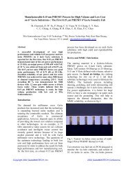
<strong>Deposition</strong> <strong>control</strong> <strong>during</strong> <strong>GaN</strong> <strong>MOVPE</strong>D. Fahle 1 , R. Puesche 2 , M. Mukinovic 2 , M. Dauelsberg 2 , R. Schreiner 2 ,H. Kalisch 1 , M. Heuken 1, 2 , A. Vescan 11 <strong>GaN</strong> Device Technology, RWTH Aachen University, 52074 Aachen, Germany2 AIXTRON SE, Kaiserstr. 98, 52134 Herzogenrath, Germanye-mail: dirk.fahle@gan.rwth-aachen.de, phone: +49-2418909105KEYWORDS: <strong>MOVPE</strong>, GAN-ON-SI, 200 MM, ETCHINGAbstractFirst we report on the growth of <strong>GaN</strong> on 200 mmsilicon (111) substrates using horizontal flow production<strong>MOVPE</strong> equipment. After optimizing and fine-tuningthe system for growth on large silicon wafers, excellentthickness and PL uniformities on 200 mm silicon, asrequested by LED chip manufacturers, aredemonstrated.Secondly, results from separate investigations on theinfluence of HCl-assisted growth impact on parasiticdeposits will be presented. This approach opens the doorfor the application of an in-situ clean after growthprocess. Adding HCl <strong>during</strong> growth of <strong>GaN</strong> significantlyreduced parasitic growth on reactor walls, which can inturn lead to significant uptime of the <strong>MOVPE</strong> reactor.INTRODUCTIONGroup III nitride based devices, such as white light emittingdiodes (LED) and heterostructure field effect transistors(HFET), have recently gained a lot of attraction. Due to theunique features of group III nitrides, these devices areconsidered to play an important role for energy saving, e.g.replacing incandescent light bulbs by LEDs or enablingmore efficient power converters.In comparison to the conventionally used sapphire substrate,Si offers both, lower costs for those wafer sizes of up to150 mm available from both materials as well as existenceof up to 450 mm in diameter. The growth of group IIInitrides on Si enables to reduce costs and to use existing150 mm and 200 mm processing infrastructure and thereforeto outperform existing technologies.Since multi-wafer <strong>MOVPE</strong> deposition tools for 200 mm alsobecome available, a transition from 150 mm to 200 mm istaking place. For the growth of <strong>GaN</strong> on Si, due to differentlattice parameters and thermal expansion coefficients,special care has to be taken for bow and strain management<strong>during</strong> deposition. By scaling up wafer size, these issues arescaled up in importance as well.To master this challenge, a lot of progress has been made tooptimize the epitaxial structure by using Al<strong>GaN</strong> transitionbuffers [1-3].The most critical step for heteroepitaxy is surfacepreparation and the growth of a nucleation layer. Therefore,to avoid a gallium contamination of the surface and the socalled gallium melt back etching [4], cleaning of the reactorbefore every run is essential. Although, an efficient cleaningof reactor parts is necessary to provide a highly reproducibleprocess, not much has been reported in literature about thistopic for group III nitrides.First we will report on the results of a modified metalorganicvapor phase epitaxy (<strong>MOVPE</strong>) reactor for 200 mmof <strong>GaN</strong> on Si deposition.Additionally we will describe a new method to minimize theamount of parasitic deposits <strong>during</strong> growth, by adding HClto the gas phase of a conventional <strong>GaN</strong> <strong>MOVPE</strong> process.GROWTH OF GAN ON 200 MM SI (111)To establish most appropriate process conditions for thegrowth of five times 200 mm wafers using the existinghorizontal flow AIX G5 production tool, the existing<strong>MOVPE</strong> platform was further upgraded by some features.The probably most important one is the transition from atriple-inlet injector towards a penta injector. This injectorfeatures five injection levels instead of three so far. Takingthis approach vey good uniformities all over the 200 mmradius are achieved. A comparison of a triple and pentainjector is shown in Fig.1. As an example the ammoniadistribution is shown for both types of injectors.Further, the heating system, gas mixing and reactor furniturewas redesigned. For distinction purposes, this reactorrevision is being labelled as, AIX G5+.With this new setup, <strong>GaN</strong> was grown on 200 mm Si (111)wafers. A reference HFET structure was deposited on SEMIstandardwafers with a thickness of 725 µm. After furthertweaking process conditions with support from simulationcalculations, as displayed in Fig. 2, a homogeneousthickness distribution is achieved, without cracking of thelayer, exhibiting a unique axis-symmetric profile.<strong>CS</strong> MANTECH Conference, May 13th - 16th, 2013, New Orleans, Louisiana, USA39912
123Figure 1: Calculated ammonia distribution for a triple(left picture) and a penta (right picture) injector.12345To show the capability to grow an LED on 200 mm Si, a5 µm thick <strong>GaN</strong> layer was grown on 1.15 mm thicksubstrates. On top, a five-fold In<strong>GaN</strong>/<strong>GaN</strong> quantum wellstructure was deposited, which gave excellent PLhomogeneity with a standard deviation of σ=1.3 nm (Fig. 4).By this, 95% of the area was in a 5 nm bin or 99.75% in 10nm bin (“bin” demonstrating a common classificationtogether with related values serving as quality criteriabetween LED manufacturers and their customers).Further, the composition of the Al<strong>GaN</strong> transition buffer wasinvestigated by HRXRD. 2Theta /Omega scans of the (0002)peaks for two consecutive runs (Fig. 3) reveal exactly thesame Al<strong>GaN</strong> compositions for different spots on thesubstrate, confirming the composition uniformity.20 nm Al<strong>GaN</strong> barrier1.4 µm <strong>GaN</strong>bufferAl<strong>GaN</strong>transitionbuffer200 mm Si725 µmThickness(µm)Figure 4: Thickness profile of a 5 µm <strong>GaN</strong> layer (withAl<strong>GaN</strong> transition layer 6 µm) on 1.15 mm thicksubstrates (left picture). In the right picture, a MQWstructure on top of this buffer resulted in a homogeneousPL distribution (σ=1.3 nm without edge exclusion).Sat 1 Sat 2 Sat 3 Sat 4 Sat 5Thickness / µm 2.21 2.22 2.21 2.22 2.21Std. dev. / % 0.90 0.90 0.90 0.90 0.81Figure 2: Thickness homogeneity of a reference HFETstructure.<strong>GaN</strong>Al x Ga 1-x Nx = 20.4%x = 43.8%x = 55.6%AlNRun 1, center(x=0mm)Run 1, center-edge(x=45mm)Run 1, edge(x=90mm)Run 2, center(x=0mm)Run 2, center-edge(x=45mm)Run 2, edge(x=90mm)Figure 3: 2Theta /Omega scans of the Al<strong>GaN</strong> transitionbuffer at the center, half radius and the wafer edge fortwo consecutive runs. No variation in composition isobserved on wafer and run-to-run.400 <strong>CS</strong> MANTECH Conference, May 13th - 16th, 2013, New Orleans, Louisiana, USA
IMPACT OF HCL DURING GROWTH ON PARASITIC DEPOSITSAs motivated in the introduction, the growth of <strong>GaN</strong> on Si issensitive to gallium contamination before or <strong>during</strong>nucleation. Sources for this contamination are parasiticdeposits on reactor walls.It is therefore of most importance to minimize the amount ofparasitic deposits formed <strong>during</strong> growth or to evencompletely remove these deposits. Hydrogen chloride (HCl)addition to the <strong>GaN</strong> process has been proven to play apositive role in limiting parasitic gas phase reactions [5].To investigate the suitability of HCl, acting both asadditional parameter for growth <strong>control</strong> and in-situ cleaningagent, we carried out the following experiments in a researchmulti-wafer <strong>MOVPE</strong> system – hotwall system [5, 6] in a 2inch wafer configuration.As described in [5], we injected HCl <strong>during</strong> the growth of<strong>GaN</strong> on sapphire.Growth rateg rCenter of Reaction Chamber (feed-inof MOs and NH 3 , HCl)InjectorCeilingTop NH 3 + H 2Top CentralMO + H 2BottomHCl + H 2Graphite SusceptorReactor radiusdistance dParasitic <strong>GaN</strong>depositsDepletion profilesubstrate2 inchFigure 5: Experimental setup, HCl is separated fromNH 3 by the central level of the injector. By introducingHCl at the bottom level, it is introduced close to the areain which the most parasitic deposits are formed. Atypical depletion profile of the growth rate in ahorizontal reactor is illustrated by the dotted line.By feeding-in HCl <strong>during</strong> growth via the lower level of theinjector, the highest concentration of HCl in the gas phase isobtained in the region between the location of injector andthe substrate edge in which most parasitic deposits occur(see Fig. 5). Before each experiment the system is thermallycleaned by a long high temperature bake (>1200°C) underhydrogen ambient to remove the remained deposits.Depending on the flow rate of HCl relative to that of TMGa,we observe that the etch-clean effect extends over a certaindistance from above mentioned region. A visible sharpchange in contrast between the cleaned and the still coatedsusceptor surface further downstream was observed, asillustrated in Fig. 6.As reference, a run without HCl was performed, <strong>during</strong>which we measured the size of parasitic deposits to be5.5 cm. With increasing HCl flow, the size of the deposits issuccessively reduced and finally diminished to 0.1 cm for anHCl flow of 16 sccm (see Fig.7).coated areauncoated areacoated areauncoated areaLocation ofInjector (if lidis closed)5.5 cmmeasured distance3.4 cmmeasured distanceReference without HClsubstrateHCl = 3 sccmsubstrateFigure 6: Pictures of the susceptor after a referencegrowth run without HCl (upper picture) and after a runwith 3 sccm HCl (lower picture). A visible sharp changein contrast marks the abrupt transition between thecleaned and coated susceptor surface (highlighted by thedashed line). The size of parasitic deposits is reduced byflowing HCl into the reactor <strong>during</strong> growth.The impact of HCl on the deposition profile on the substrateis shown in Fig. 8. Substrates were deliberately blockedfrom rotating in order to study the effect of HCl on thedeposition profile along the reactor radius without averagingthe profile over the wafer by rotation. Up to an HCl flow of3 sccm, the deposition profile is not affected by HCl. Noincrease in growth rate was observed. Contrary, we observeda decrease in growth rate at an HCl flow of 9 sccm HCl,which did not influence the form of the deposition profilesignificantly. For the case of 9 sccm, not all deposits wereremoved upstream the substrate, but the growth rate wasalready reduced to 0.8 times of that of the reference. Furtherincreasing of HCl flow made the deposits upstream thewafer disappear and only some deposits left on the areabetween the satellites. At these conditions, the depositionprofile on the wafer were considerable affected and thegrowth rate was reduced by half. Once all parasitic depositsare consumed by HCl, some of the remaining HCl reachesthe substrate acts as an etchant on the <strong>GaN</strong> film. Therefore, alower growth rate is observed.As we never observed an increase of growth rate, weconclude that gallium chlorides formed from parasiticdeposits do not contribute to deposition on substrate.Experiments on the etch rate of aluminium-containing layersrevealed that the etch rate is much lower and hightemperatures would be needed. E.g., for etching AlN byHCl, a temperature higher than 1300°C is required but<strong>CS</strong> MANTECH Conference, May 13th - 16th, 2013, New Orleans, Louisiana, USA40112
yielding a low etch rate. For these materials, a Cl 2 etchprocess is more suitable which also gives higher etch rateson <strong>GaN</strong>, which we will report on elsewhere.Size of parasitic deposit zone (cm)6420HCl flux (sccm)0 2 4 6 8 10 12 14 160.0 0.2 0.4 0.6 0.8 1.0 1.2Molar ratio (HCl:TMGa)Figure 7: Reduction of the parasitic deposits. The size ofparasitic deposits is measured as distance betweensubstrate and transition between the clean susceptorsurface and still coated surface. With increasing HClflow, the amount of parasitic deposits is significantlyreduced.Growth rate (µm/h)3.02.52.01.51.00.5HCl = 0 sccmHCl = 1 sccmHCl = 3 sccmHCl = 9 sccmHCl = 16 sccmFor the use of HCl <strong>during</strong> growth, we observed asignificantly reduced coating of the reactor entrance area,upstream of the substrate. Although for high flows of HCl,all parasitic deposits were converted to gallium chlorides,these species did not contribute to the growth on thesubstrate. Further, the results show the suitability of HCl foran in-situ clean for <strong>GaN</strong> deposits. For Al<strong>GaN</strong>- or AlNcontainingparasitic deposits, a more reactive gas like Cl 2 isrequired to obtain reasonable etch rates.REFERENCES[1] A. Dadgar et al., Journal of Crystal Growth 248 p.556–562(2003)[2] A. Krost, A. Dadgar, G. Strassburger, R. Clos, physica status solidi (a),vol 200, Issue 1, p. 26–35 (2003)[3] K. Cheng, M. Leys, S. Degroote, B. Van Daele, S. Boeykens, J.Derluyn, M. Germain, G. Van Tendeloo, J. Engelen, G. Borghs, Journalof Electronic Materials 2006, Volume 35, Issue 4, pp 592-598[4] A. Krost, A. Dadgar, Materials Science and Engineering: B 93 (1),p.77-84 (2002)[5] D. Fahle, D. Brien, M. Dauelsberg, G. Strauch, M. Heuken, H. Kalisch,A. Vescan, J. Cryst. Growth, accepted for publication(http://dx.doi.org/10.1016/j.jcrysgro.2012.10.027)[6] D. Fahle, H. Behmenburg, C. Mauder, H. Kalisch, R. Jansen, H.Kitahata, D. Brien, G. Strauch, D. Schmitz, M. Heuken, Phys. StatusSolidi C, p. 2041-2043 (2011)ACRONYMSMO : Metal-Organic<strong>MOVPE</strong>: Metal-Organic Chemical Vapor EpitaxyPL: PhotoluminescenceHRXRD: High Resolution X-RayDiffraction0.0120 130 140 150 160 170Reactor radius (mm)Figure 8: <strong>Deposition</strong> profiles on substrate for differentHCl flows <strong>during</strong> growth. The growth rate is reducedabove an HCl flow of 9 sccm. For an HCl flow of 16sccm, the shape of the profile is affected due to surfaceetching.CONCLUSIONSWe have demonstrated the growth of <strong>GaN</strong> on 200 mm Sisubstrates. By optimizing the design of the reactor, weenabled the deposition on SEMI-standard wafers for HFETapplications. Furthermore, we demonstrated on top of a6 µm thick crack-free <strong>GaN</strong> layer an In<strong>GaN</strong>/<strong>GaN</strong> MQWstructure with excellent PL homogeneity.402 <strong>CS</strong> MANTECH Conference, May 13th - 16th, 2013, New Orleans, Louisiana, USA