NTE3097 Optoisolator Zero Crossing TRIAC Driver
NTE3097 Optoisolator Zero Crossing TRIAC Driver
NTE3097 Optoisolator Zero Crossing TRIAC Driver

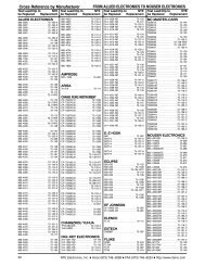
You also want an ePaper? Increase the reach of your titles
YUMPU automatically turns print PDFs into web optimized ePapers that Google loves.
<strong>NTE3097</strong><strong>Optoisolator</strong><strong>Zero</strong> <strong>Crossing</strong> <strong>TRIAC</strong> <strong>Driver</strong>Description:The <strong>NTE3097</strong> is an optoisolator in a 6–Lead DIP type package and contains a gallium arsenide IREDoptically coupled to a monolithic silicon detector performing the function of a <strong>Zero</strong> Voltage <strong>Crossing</strong>bilateral <strong>TRIAC</strong> <strong>Driver</strong>. This device is designed for use with a <strong>TRIAC</strong> in the interface of logic systemsto equipment powered from 240VAC lines such as solid–state relays, industrial controls, motors, solenoids,and consumer appliances, etc.Features: Simplifies Logic Control of 240VAC Power <strong>Zero</strong> Voltage <strong>Crossing</strong> High Breakdown Voltage: V DRM = 400V Min High Isolation Voltage: V ISO = 7500V Guaranteed Small, Economical 6–Lead DIP Package dv/dt of 2000V/µs Typ., 1000V/µs GuaranteedAbsolute Maximum Rating: (T A = +25°C unless otherwise specified)Infrared Emitting DiodeReverse Voltage, V R . . . . . . . . . . . . . . . . . . . . . . . . . . . . . . . . . . . . . . . . . . . . . . . . . . . . . . . . . . . . . . . . . 6VContinuous Forward Current, I F . . . . . . . . . . . . . . . . . . . . . . . . . . . . . . . . . . . . . . . . . . . . . . . . . . . . 60mATotal Power Dissipation (T A = +25°C, Negligible Power in Output <strong>Driver</strong>),P D . . . . . . . . . . . . 120mWDerate Above 25°C . . . . . . . . . . . . . . . . . . . . . . . . . . . . . . . . . . . . . . . . . . . . . . . . . . . . 1.41mW/°COutput <strong>Driver</strong>Off–State Output Terminal Voltage, V DRM . . . . . . . . . . . . . . . . . . . . . . . . . . . . . . . . . . . . . . . . . . . . . 400VPeak Repetitive Surge Current (PW = 100µs, 120pps), I TSM . . . . . . . . . . . . . . . . . . . . . . . . . . . . . . 1ATotal Power Dissipation (T A = +25°C),P D . . . . . . . . . . . . . . . . . . . . . . . . . . . . . . . . . . . . . . . . . . . 150mWDerate Above 25°C . . . . . . . . . . . . . . . . . . . . . . . . . . . . . . . . . . . . . . . . . . . . . . . . . . . . 1.76mW/°CTotal DeviceIsolation Surge Voltage (Peak AC Voltage, 60Hz, 1sec Duration, Note 1), V ISO . . . . . . . . . . . 7500VTotal Power Dissipation (T A = +25°C),P D . . . . . . . . . . . . . . . . . . . . . . . . . . . . . . . . . . . . . . . . . . . 250mWDerate Above 25°C . . . . . . . . . . . . . . . . . . . . . . . . . . . . . . . . . . . . . . . . . . . . . . . . . . . . 2.94mW/°CJunction Temperature Range, T J . . . . . . . . . . . . . . . . . . . . . . . . . . . . . . . . . . . . . . . . . . . –40° to +100°CAmbient Operating Temperature Range, T A . . . . . . . . . . . . . . . . . . . . . . . . . . . . . . . . . . . –40° to +85°CStorage Temperature Range, T stg . . . . . . . . . . . . . . . . . . . . . . . . . . . . . . . . . . . . . . . . . . –40° to +150°CLead Temperature (During Soldering, 10sec), T L . . . . . . . . . . . . . . . . . . . . . . . . . . . . . . . . . . . . +260°CNote 1. Isolation surge voltage is an internal dielectric breakdown rating. For this test, Pin1 and Pin2are common, and Pin4, Pin5, and Pin6 are common.
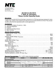
Electrical Characteristics: (T A = +25°C unless otherwise specified)Input LEDParameter Symbol Test Conditions Min Typ Max UnitReverse Leakage Current I R V R = 6V – 0.05 10 µAForward Voltage V F I F = 30mA – 1.3 1.5 VOutput Detector (I F = 0 unless otherwise specified)Leakage With LED OFF I DRM1 Either Direction, V DRM = 400V, Note 2 – 2 100 nAPeak On–State Voltage V TM Either Direction, I TM = 100mA Peak – 1.8 3.0 VCritical Rate of Rise ofOff–State VoltageCoupleddv/dt Note 4 1000 2000 – V/µsLED Trigger Current, I FT Main Terminal Voltage = 3V, Note 3 – – 15 mACurrent Required toLatch OutputHolding Current I H Either Direction – 100 – µAIsolation Voltage V ISO f = 60Hz, t = 1sec 7500 – – VAC(pk)<strong>Zero</strong> <strong>Crossing</strong>Inhibit Voltage V IH I F = 15mA, MT1–MT2 Voltage Above – 5 20 VWhich Device Will Not TriggerLeakage in Inhibit State I DRM2 I F = 15mA, V DRM = 400V, Off–State – – 500 µANote 2. Test voltage must be applied within dv/dt rating.Note 3. This device is guaranteed to trigger at an I F1 value less than or equal to max. I FT . Therefore,recommended operating I F lies between max. I FT (15mA) and absolute max. I F (60mA).Note 4. This is static dv/dt. Commutating dv/dt is a function of the load–driving thyristor only.Pin Connection Diagram65 41 2 3.260(6.6)MaxAnodeCathodeN.C.123ZEROCROSSINGCIRCUIT654Main TerminalSubstrateDo Not ConnectMain Terminal.070 (1.78)Max.350 (8.89)Max.200 (5.08)Max.350(8.89)Max.300 (7.62).085 (2.16)Max.100 (2.54)