Planck Pre-Launch Status Papers - APC - Université Paris Diderot ...
Planck Pre-Launch Status Papers - APC - Université Paris Diderot ...
Planck Pre-Launch Status Papers - APC - Université Paris Diderot ...

You also want an ePaper? Increase the reach of your titles
YUMPU automatically turns print PDFs into web optimized ePapers that Google loves.
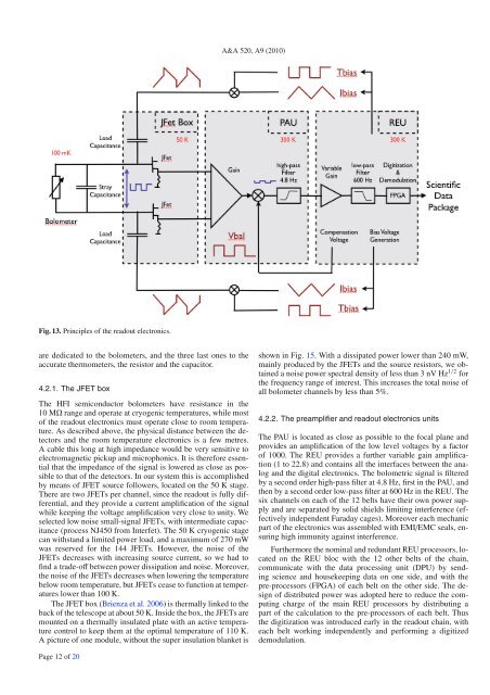
A&A 520, A9 (2010)Fig. 13. Principles of the readout electronics.are dedicated to the bolometers, and the three last ones to theaccurate thermometers, the resistor and the capacitor.4.2.1. The JFET boxThe HFI semiconductor bolometers have resistance in the10 MΩ range and operate at cryogenic temperatures, while mostof the readout electronics must operate close to room temperature.As described above, the physical distance between the detectorsand the room temperature electronicsisafewmetres.Acablethislongathighimpedancewouldbeverysensitivetoelectromagnetic pickup and microphonics. It is therefore essentialthat the impedance of the signal is lowered as close as possibleto that of the detectors. In our system this is accomplishedby means of JFET source followers, located on the 50 K stage.There are two JFETs per channel, since the readout is fully differential,and they provide a current amplification of the signalwhile keeping the voltage amplification very close to unity. Weselected low noise small-signal JFETs, with intermediate capacitance(process NJ450 from Interfet). The 50 K cryogenic stagecan withstand a limited power load, and a maximum of 270 mWwas reserved for the 144 JFETs. However, the noise of theJFETs decreases with increasing sourcecurrent,sowehadtofind a trade-off between power dissipation and noise. Moreover,the noise of the JFETs decreases when lowering the temperaturebelow room temperature, but JFETs cease to function at temperatureslower than 100 K.The JFET box (Brienza et al. 2006)isthermallylinkedtotheback of the telescope at about 50 K. Inside the box, the JFETs aremounted on a thermally insulated plate with an active temperaturecontrol to keep them at the optimal temperature of 110 K.Apictureofonemodule,withoutthesuperinsulationblanketisshown in Fig. 15. Withadissipatedpowerlowerthan240mW,mainly produced by the JFETs and the source resistors, we obtaineda noise power spectral density of less than 3 nV Hz 1/2 forthe frequency range of interest. This increases the total noise ofall bolometer channels by less than 5%.4.2.2. The preamplifier and readout electronics unitsThe PAU is located as close as possible to the focal plane andprovides an amplification of the low level voltages by a factorof 1000. The REU provides a further variable gain amplification(1 to 22.8) and contains all the interfaces between the analogand the digital electronics. The bolometric signal is filteredby a second order high-pass filter at 4.8 Hz, first in the PAU, andthen by a second order low-pass filter at 600 Hz in the REU. Thesix channels on each of the 12 belts have their own power supplyand are separated by solid shields limiting interference (effectivelyindependent Faraday cages). Moreover each mechanicpart of the electronics was assembled with EMI/EMC seals, ensuringhigh immunity against interference.Furthermore the nominal and redundant REU processors, locatedon the REU bloc with the 12 other belts of the chain,communicate with the data processing unit (DPU) by sendingscience and housekeeping data on one side, and with thepre-processors (FPGA) of each belt on the other side. The designof distributed power was adopted here to reduce the computingcharge of the main REU processors by distributing apart of the calculation to the pre-processors of each belt. Thusthe digitization was introduced early in the readout chain, witheach belt working independently and performing a digitizeddemodulation.Page 12 of 20