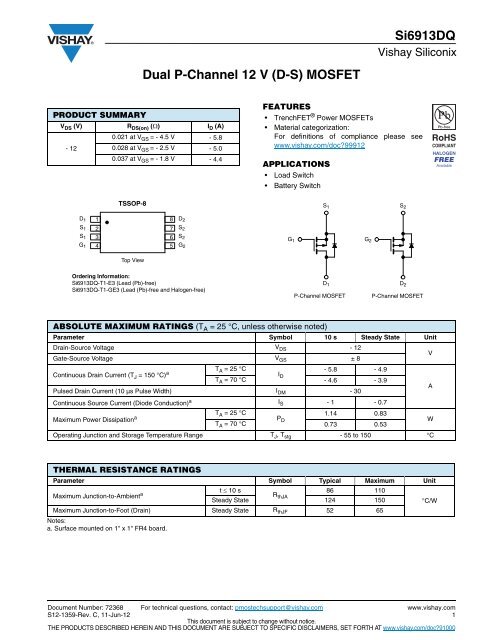
Si6913DQ Dual P-Channel 12 V (D-S) MOSFET - Vishay
Si6913DQ Dual P-Channel 12 V (D-S) MOSFET - Vishay
Si6913DQ Dual P-Channel 12 V (D-S) MOSFET - Vishay

Create successful ePaper yourself
Turn your PDF publications into a flip-book with our unique Google optimized e-Paper software.
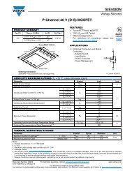
<strong>Si6913DQ</strong><strong>Vishay</strong> Siliconix<strong>Dual</strong> P-<strong>Channel</strong> <strong>12</strong> V (D-S) <strong>MOSFET</strong>PRODUCT SUMMARYV DS (V) R DS(on) () I D (A)0.021 at V GS = - 4.5 V - 5.8- <strong>12</strong>0.028 at V GS = - 2.5 V - 5.00.037 at V GS = - 1.8 V - 4.4FEATURES• TrenchFET ® Power <strong>MOSFET</strong>s• Material categorization:For definitions of compliance please seewww.vishay.com/doc?999<strong>12</strong>APPLICATIONS• Load Switch• Battery SwitchTSSOP-8S 1S 2D 1 1S 1 2S 1 3G 1 48765D 2S 2S 2G 2G 1D 1G 2D 2Top ViewOrdering Information:<strong>Si6913DQ</strong>-T1-E3 (Lead (Pb)-free)<strong>Si6913DQ</strong>-T1-GE3 (Lead (Pb)-free and Halogen-free)P-<strong>Channel</strong> <strong>MOSFET</strong>P-<strong>Channel</strong> <strong>MOSFET</strong>ABSOLUTE MAXIMUM RATINGS (T A = 25 °C, unless otherwise noted)Parameter Symbol 10 s Steady State UnitDrain-Source Voltage V DS - <strong>12</strong>VGate-Source Voltage V GS ± 8Continuous Drain Current (T J = 150 °C) a T A = 25 °C- 5.8 - 4.9I DT A = 70 °C - 4.6 - 3.9APulsed Drain Current (10 µs Pulse Width) I DM - 30Continuous Source Current (Diode Conduction) a I S - 1 - 0.7T A = 25 °CMaximum Power Dissipation a 1.14 0.83P D WT A = 70 °C 0.73 0.53Operating Junction and Storage Temperature Range T J , T stg - 55 to 150 °CTHERMAL RESISTANCE RATINGSParameter Symbol Typical Maximum UnitMaximum Junction-to-Ambient at 10 s86 110R thJASteady State <strong>12</strong>4 150°C/WMaximum Junction-to-Foot (Drain) Steady State R thJF 52 65Notes:a. Surface mounted on 1" x 1" FR4 board.Document Number: 72368S<strong>12</strong>-1359-Rev. C, 11-Jun-<strong>12</strong>For technical questions, contact: pmostechsupport@vishay.comwww.vishay.com1This document is subject to change without notice.THE PRODUCTS DESCRIBED HEREIN AND THIS DOCUMENT ARE SUBJECT TO SPECIFIC DISCLAIMERS, SET FORTH AT www.vishay.com/doc?91000
<strong>Si6913DQ</strong><strong>Vishay</strong> SiliconixDrain-Source On-State Resistance a R DS(on)SPECIFICATIONS (T J = 25 °C, unless otherwise noted)Parameter Symbol Test Conditions Min. Typ. Max. UnitStaticGate Threshold Voltage V GS(th) V DS = V GS , I D = - 400 µA - 0.4 - 0.9 VGate-Body Leakage I GSS V DS = 0 V, V GS = ± 8 V ± 100 nAV DS = - <strong>12</strong> V, V GS = 0 V - 1Zero Gate Voltage Drain Current I DSSV DS = - <strong>12</strong> V, V GS = 0 V, T J = 70 °C - 25µAOn-State Drain Current a I D(on) V DS - 5 V, V GS = - 4.5 V - 20 AV GS = - 2.5 V, I D = - 5 A 0.021 0.028 V GS - 4.5 V, I D = - 5.8 A 0.016 0.021V GS = - 1.8 V, I D = - 4.4 A 0.029 0.037Forward Transconductance a g fs V DS = - 5 V, I D = - 5.8 A 25 SDiode Forward Voltage a V SD I S = - 1 A, V GS = 0 V - 0.61 - 1.1 VDynamic bTotal Gate ChargeQ g18.5 28Gate-Source Charge Q gs V DS = - 6 V, V GS = - 4.5 V, I D = - 5.8 A2.7nCGate-Drain Charge Q gd 5Gate Resistance R g f = 1 MHz 4.6 Turn-On Delay Timet d(on)45 70Rise Time t r V DD = - 6 V, R L = 6 80 <strong>12</strong>0Turn-Off Delay Time t d(off) I D - 1 A, V GEN = - 4.5 V, R G = 6 130 200 nsFall Time t f 80 <strong>12</strong>0Source-Drain Reverse Recovery Time t rr I F = - 1 A, dI/dt = 100 A/µs 65 100Notes:a. Pulse test; pulse width 300 µs, duty cycle 2 %.b. Guaranteed by design, not subject to production testing.Stresses beyond those listed under “Absolute Maximum Ratings” may cause permanent damage to the device. These are stress ratings only, and functional operationof the device at these or any other conditions beyond those indicated in the operational sections of the specifications is not implied. Exposure to absolute maximumrating conditions for extended periods may affect device reliability.TYPICAL CHARACTERISTICS (25 °C, unless otherwise noted)30V GS = 5 thru 2.5 V2 V30T C = - 55 °C242425 °C- Drain Current (A)I D18<strong>12</strong>61.5 V- Drain Current (A)I D18<strong>12</strong>6<strong>12</strong>5 °C00 1 2 3 4 5V DS - Drain-to-Source Voltage (V)Output Characteristics00.0 0.5 1.0 1.5 2.0 2.5V GS - Gate-to-Source Voltage (V)Transfer CharacteristicsDocument Number: 72368S<strong>12</strong>-1359-Rev. C, 11-Jun-<strong>12</strong>For technical questions, contact: pmostechsupport@vishay.comwww.vishay.com2This document is subject to change without notice.THE PRODUCTS DESCRIBED HEREIN AND THIS DOCUMENT ARE SUBJECT TO SPECIFIC DISCLAIMERS, SET FORTH AT www.vishay.com/doc?91000
<strong>Si6913DQ</strong><strong>Vishay</strong> SiliconixTYPICAL CHARACTERISTICS (25 °C, unless otherwise noted)0.103500R DS(on) - On-Resistance ()0.080.060.040.02V GS = 1.8 VV GS = 2.5 VV GS = 4.5 VC - Capacitance (pF)30002500200015001000500C rssC ossC iss0.000 5 10 15 20 25 30I D - Drain Current (A)On-Resistance vs. Drain Current00 2 4 6 8 10 <strong>12</strong>V DS - Drain-to-Source Voltage (V)Capacitance61.6- Gate-to-Source Voltage (V)5432V DS = 6 VI D = 5.8 A- On-Resistance (Normalized)1.41.21.0V GS = 4.5 VI D = 5.8 AV GS1R DS(on)0.800 5 10 15 20 25 30Q g - Total Gate Charge (nC)Gate Charge0.6- 50 - 25 0 25 50 75 100 <strong>12</strong>5 150T J - Junction Temperature (°C)On-Resistance vs. Junction Temperature300.08- Source Current (A)I S101T J = 150 °CT J = 25 °CR DS(on) - On-Resistance ()0.070.060.050.040.030.02I D = 5.8 A0.010.10.0 0.3 0.6 0.9 1.2 1.5V SD - Source-to-Drain Voltage (V)Source-Drain Diode Forward Voltage0.000 1 2 3 4 5 6 7 8V GS - Gate-to-Source Voltage (V)On-Resistance vs. Gate-to-Source VoltageDocument Number: 72368S<strong>12</strong>-1359-Rev. C, 11-Jun-<strong>12</strong>For technical questions, contact: pmostechsupport@vishay.comwww.vishay.com3This document is subject to change without notice.THE PRODUCTS DESCRIBED HEREIN AND THIS DOCUMENT ARE SUBJECT TO SPECIFIC DISCLAIMERS, SET FORTH AT www.vishay.com/doc?91000
<strong>Si6913DQ</strong><strong>Vishay</strong> SiliconixTYPICAL CHARACTERISTICS (25 °C, unless otherwise noted)0.41000.380Variance (V)V GS(th)0.20.10.0I D = 400 µAPower (W)6040- 0.<strong>12</strong>0- 0.2- 50 - 25 0 25 50 75 100 <strong>12</strong>5 150T J - Temperature (°C)Threshold Voltage00.001 0.01 0.1 110Time (s)Single Pulse Power, Junction-to-Ambient100Limited by R * DS(on)- Drain Current (A)I D1010.1T C = 25 °CSingle Pulse1 ms10 ms100 ms1 s10 sDC0.010.1 1 10 100V DS - Drain-to-Source Voltage (V)*V GS > minimum V GS at which R DS(on) is specifiedSafe Operating Area, Junction-to-Case2Normalized Effective TransientThermal Impedance10.1Duty Cycle = 0.50.20.10.050.023. T JM - T A = P DM Z (t) thJASingle Pulse4. Surface Mounted0.0110 -4 10 -3 10 -2 10 -11 10 100600Square Wave Pulse Duration (s)Notes:P DMNormalized Thermal Transient Impedance, Junction-to-Ambientt 1t 2 t 11. Duty Cycle, D =t 22. Per Unit Base = R thJA = <strong>12</strong>4 °C/WDocument Number: 72368S<strong>12</strong>-1359-Rev. C, 11-Jun-<strong>12</strong>For technical questions, contact: pmostechsupport@vishay.comwww.vishay.com4This document is subject to change without notice.THE PRODUCTS DESCRIBED HEREIN AND THIS DOCUMENT ARE SUBJECT TO SPECIFIC DISCLAIMERS, SET FORTH AT www.vishay.com/doc?91000
<strong>Si6913DQ</strong><strong>Vishay</strong> SiliconixTYPICAL CHARACTERISTICS (25 °C, unless otherwise noted)2Normalized Effective TransientThermal Impedance10.1Duty Cycle = 0.50.20.10.050.02Single Pulse0.0110 -410 -3 10 -2 1 10Square Wave Pulse Duration (s)Normalized Thermal Transient Impedance, Junction-to-Foot10 -1<strong>Vishay</strong> Siliconix maintains worldwide manufacturing capability. Products may be manufactured at one of several qualified locations. Reliability data for SiliconTechnology and Package Reliability represent a composite of all qualified locations. For related documents such as package/tape drawings, part marking, andreliability data, see www.vishay.com/ppg?72368.Document Number: 72368S<strong>12</strong>-1359-Rev. C, 11-Jun-<strong>12</strong>For technical questions, contact: pmostechsupport@vishay.comwww.vishay.com5This document is subject to change without notice.THE PRODUCTS DESCRIBED HEREIN AND THIS DOCUMENT ARE SUBJECT TO SPECIFIC DISCLAIMERS, SET FORTH AT www.vishay.com/doc?91000
Package Information<strong>Vishay</strong> SiliconixJEDEC Part Number: MO-153R 0.10Corners)AA2A1BDeE1CR 0.10(4 Corners)ELL10.25 (Gage Plane)K1Dim Min Nom MaxA – – 1.20A 1 0.05 0.10 0.15A 2 0.80 1.00 1.05B 0.19 0.28 0.30C – 0.<strong>12</strong>7 –D 2.90 3.00 3.10E 6.20 6.40 6.60E 1 4.30 4.40 4.50e – 0.65 –L 0.45 0.60 0.75L 1 0.90 1.00 1.10Y – – 0.10K1 0 3 6ECN: S-03946—Rev. G, 09-Jul-01DWG: 5844Document Number: 7<strong>12</strong>0106-Jul-01www.vishay.com1
LITTLE FOOT TSSOP-8The Next Step in Surface-Mount Power <strong>MOSFET</strong>sAN1001<strong>Vishay</strong> SiliconixWharton McDaniel and David OldhamWhen <strong>Vishay</strong> Siliconix introduced its LITTLE FOOT<strong>MOSFET</strong>s, it was the first time that power <strong>MOSFET</strong>s had beenoffered in a true surface-mount package, the SOIC. LITTLEFOOT immediately found a home in new small form factor diskdrives, computers, and cellular phones.The new LITTLE FOOT TSSOP-8 power <strong>MOSFET</strong>s are thenatural evolutionary response to the continuing demands ofmany markets for smaller and smaller packages. LITTLEFOOT TSSOP-8 <strong>MOSFET</strong>s have a smaller footprint and alower profile than LITTLE FOOT SOICs, while maintaining lowr DS(on) and high thermal performance. <strong>Vishay</strong> Siliconix hasaccomplished this by putting one or two high-density <strong>MOSFET</strong>die in a standard 8-pin TSSOP package mounted on a customleadframe.THE TSSOP-8 PACKAGEThis is the low profile demanded by applications such asPCMCIA cards.It reduces the power package to the same height as manyresistors and capacitors in 0805 and 0605 sizes. It also allowsplacement on the “passive” side of the PC board.The standard pinouts of the LITTLE FOOT TSSOP-8packages have been changed from the standard establishedby LITTLE FOOT. This change minimizes the contribution ofinterconnection resistance to r DS(on) and maximizes thetransfer of heat out of the package.Figure 2 shows the pinouts for a single-die TSSOP. Notice thatboth sides of the package have Source and Drainconnections, whereas LITTLE FOOT has the Source and Gateconnections on one side of the package, and the Drainconnections are on the opposite side.LITTLE FOOT TSSOP-8 power <strong>MOSFET</strong>s requireapproximately half the PC board area of an equivalent LITTLEFOOT device (Figure 1). In addition to the reduction in boardarea, the package height has been reduced to 1.1 mm.DrainSourceSourceGateDrainSourceSourceDrainFigure 2.Pinouts for Single Die TSSOPTop ViewFigure 3 shows the standard pinouts for a dual-die TSSOP-8.In this case, the connections for each individual <strong>MOSFET</strong>occupy one side.Side ViewDrain 1Source 1Source 1Gate 1Drain 2Source 2Source 2Gate 2Figure 1.An TSSOP-8 Package Next to a SOIC-8 Packagewith Views from Both Top and SideFigure 3.Pinouts for <strong>Dual</strong>-Die TSSOPDocument Number: 70571<strong>12</strong>-Dec-03www.vishay.com1
AN1001<strong>Vishay</strong> SiliconixBecause the TSSOP has a fine pitch foot print, the pad layoutis somewhat more demanding than the layout of the SOIC.Careful attention must be paid to silkscreen-to-pad andsoldermask-to-pad clearances. Also, fiduciary marks may berequired. The design and spacing of the pads must be dealtwith carefully. The pads must be sized to hold enough solderpaste to form a good joint, but should not be so large or soplaced as to extend under the body, increasing the potential forsolder bridging. The pad pattern should allow for typical pickand place errors of 0.25 mm. See Application Note 826,Recommended Minimum Pad Patterns With OutlineDrawing Access for <strong>Vishay</strong> Siliconix <strong>MOSFET</strong>s,(http://www.vishay.com/doc?72286), for the recommendedpad pattern for PC board layout.THERMAL ISSUESLITTLE FOOT TSSOP <strong>MOSFET</strong>s have been given thermalratings using the same methods used for LITTLE FOOT. Themaximum thermal resistance junction-to-ambient is 83C/Wfor the single die and <strong>12</strong>5C/W for dual-die parts. TSSOP relieson a leadframe similar to LITTLE FOOT to remove heat fromthe package. The single- and dual-die leadframes are shownin Figure 4.Figure 5.The actual test is based on dissipating a known amount ofpower in the device for a known period of time so the junctiontemperature is raised to 150C. The starting and endingjunction temperatures are determined by measuring theforward drop of the body diode. The thermal resistance for thatpulse width is defined by the temperature rise of the junctionabove ambient and the power of the pulse, Tja/P.Figure 6 shows the single pulse power curve of the Si6436DQlaid over the curve of the Si9936DY to give a comparison of thethermal performance. The die in the two devices haveequivalent die areas, making this a comparison of thepackaging. This comparison shows that the TSSOP packageperforms as well as the SOIC out to 150 ms, with long-termperformance being 0.5 W less. Although the thermalperformance is less, LITTLE FOOT TSSOP will operate in alarge percentage of applications that are currently beingserved by LITTLE FOOT.14.0<strong>12</strong>.010.0a) 8-Pin Single-Pad TSSOPPower (W)8.06.04.0Si99362.0Si6436www.vishay.com2b) 8-Pin <strong>Dual</strong>-Pad TSSOPFigure 4.LeadframeThe <strong>MOSFET</strong>s are characterized using a single pulse powertest. For this test the device mounted on a one-square-inchpiece of copper clad FR-4 PC board, such as those shown inFigure 5. The single pulse power test determines themaximum amount of power the part can handle for a givenpulse width and defines the thermal resistancejunction-to-ambient. The test is run for pulse widths rangingfrom approximately 10 ms to 100 seconds. The thermalresistance at 30 seconds is the rated thermal resistance for thepart. This rating was chosen to allow comparison of packagesand leadframes. At longer pulse widths, the PC board thermalcharateristics become dominant, making all parts look thesame.0.00.1 1 10 100Time (Sec.)Figure 6. Comparison of Thermal PerformanceCONCLUSIONTSSOP power <strong>MOSFET</strong>s provide a significant reduction in PCboard footprint and package height, allowing reduction inboard size and application where SOICs will not fit. This isaccomplished using a standard IC package and a customleadframe, combining small size with good power handlingcapability.For the TSSOP-8 package outline visit:http://www.vishay.com/doc?7<strong>12</strong>01For the SOIC-8 package outline visit:http://www.vishay.com/doc?71192Document Number: 70571<strong>12</strong>-Dec-03
AN806<strong>Vishay</strong> SiliconixMounting LITTLE FOOT TSSOP-8 Power <strong>MOSFET</strong>sWharton McDanielSurface-mounted LITTLE FOOT power <strong>MOSFET</strong>s use integratedcircuit and small-signal packages which have been been modifiedto provide the heat transfer capabilities required by power devices.Leadframe materials and design, molding compounds, and dieattach materials have been changed, while the footprint of thepackages remains the same.See Application Note 826, Recommended Minimum PadPatterns With Outline Drawing Access for <strong>Vishay</strong> Siliconix<strong>MOSFET</strong>, (http://www.vishay.com/doc?72286), for the basisof the pad design for a LITTLE FOOT TSSOP-8 power <strong>MOSFET</strong>package footprint. In converting the footprint to the pad set for apower device, designers must make two connections: an electricalconnection and a thermal connection, to draw heat away from thepackage.In the case of the TSSOP-8 package, the thermal connectionsare very simple. Pins 1, 5, and 8 are the drain of the <strong>MOSFET</strong>for a single <strong>MOSFET</strong> package and are connected together. Inthe dual package, pins 1 and 8 are the two drains. For asmall-signal device or integrated circuit, typical connectionswould be made with traces that are 0.020 inches wide. Sincethe drain pins also provide the thermal connection to thepackage, this level of connection is inadequate. The totalcross section of the copper may be adequate to carry thecurrent required for the application, but it presents a largethermal impedance. Also, heat spreads in a circular fashionfrom the heat source. In this case the drain pins are the heatsources when looking at heat spread on the PC board.The pad patterns with copper spreading for the single-<strong>MOSFET</strong>TSSOP-8 (Figure 1) and dual-<strong>MOSFET</strong> TSSOP-8 (Figure 2)show the starting point for utilizing the board area available for theheat-spreading copper. To create this pattern, a plane of copperoverlies the drain pins. The copper plane connects the drain pinselectrically, but more importantly provides planar copper to drawheat from the drain leads and start the process of spreading theheat so it can be dissipated into the ambient air. These patternsuse all the available area underneath the body for this purpose.0.0320.80.0180.450.0731.780.0911.650.2847.60.0260.660.<strong>12</strong>23.1FIGURE 2. <strong>Dual</strong> <strong>MOSFET</strong> TSSOP-8 Pad Pattern withCopper SpreadingSince surface-mounted packages are small, and reflow solderingis the most common way in which these are affixed to the PCboard, “thermal” connections from the planar copper to the padshave not been used. Even if additional planar copper area is used,there should be no problems in the soldering process. The actualsolder connections are defined by the solder mask openings. Bycombining the basic footprint with the copper plane on the drainpins, the solder mask generation occurs automatically.0.0320.80.0180.450.2847.60.0260.660.<strong>12</strong>23.1A final item to keep in mind is the width of the power traces. Theabsolute minimum power trace width must be determined by theamount of current it has to carry. For thermal reasons, thisminimum width should be at least 0.020 inches. The use of widetraces connected to the drain plane provides a low impedancepath for heat to move away from the device.0.0731.780.1183.54FIGURE 1. Single <strong>MOSFET</strong> TSSOP-8 PadPattern with Copper SpreadingDocument Number: 7073817-Dec-03www.vishay.com1
Application Note 826<strong>Vishay</strong> SiliconixRECOMMENDED MINIMUM PADS FOR TSSOP-80.092(2.337)0.026(0.660)0.040(1.016)0.262(6.655)0.182(4.623)0.014(0.356)0.0<strong>12</strong>(0.305)Recommended Minimum PadsDimensions in Inches/(mm)Return to IndexReturn to IndexAPPLICATION NOTEDocument Number: 72611www.vishay.comRevision: 21-Jan-08 27
www.vishay.comLegal Disclaimer Notice<strong>Vishay</strong>DisclaimerALL PRODUCT, PRODUCT SPECIFICATIONS AND DATA ARE SUBJECT TO CHANGE WITHOUT NOTICE TO IMPROVERELIABILITY, FUNCTION OR DESIGN OR OTHERWISE.<strong>Vishay</strong> Intertechnology, Inc., its affiliates, agents, and employees, and all persons acting on its or their behalf (collectively,“<strong>Vishay</strong>”), disclaim any and all liability for any errors, inaccuracies or incompleteness contained in any datasheet or in any otherdisclosure relating to any product.<strong>Vishay</strong> makes no warranty, representation or guarantee regarding the suitability of the products for any particular purpose orthe continuing production of any product. To the maximum extent permitted by applicable law, <strong>Vishay</strong> disclaims (i) any and allliability arising out of the application or use of any product, (ii) any and all liability, including without limitation special,consequential or incidental damages, and (iii) any and all implied warranties, including warranties of fitness for particularpurpose, non-infringement and merchantability.Statements regarding the suitability of products for certain types of applications are based on <strong>Vishay</strong>’s knowledge of typicalrequirements that are often placed on <strong>Vishay</strong> products in generic applications. Such statements are not binding statementsabout the suitability of products for a particular application. It is the customer’s responsibility to validate that a particularproduct with the properties described in the product specification is suitable for use in a particular application. Parametersprovided in datasheets and/or specifications may vary in different applications and performance may vary over time. Alloperating parameters, including typical parameters, must be validated for each customer application by the customer’stechnical experts. Product specifications do not expand or otherwise modify <strong>Vishay</strong>’s terms and conditions of purchase,including but not limited to the warranty expressed therein.Except as expressly indicated in writing, <strong>Vishay</strong> products are not designed for use in medical, life-saving, or life-sustainingapplications or for any other application in which the failure of the <strong>Vishay</strong> product could result in personal injury or death.Customers using or selling <strong>Vishay</strong> products not expressly indicated for use in such applications do so at their own risk. Pleasecontact authorized <strong>Vishay</strong> personnel to obtain written terms and conditions regarding products designed for such applications.No license, express or implied, by estoppel or otherwise, to any intellectual property rights is granted by this document or byany conduct of <strong>Vishay</strong>. Product names and markings noted herein may be trademarks of their respective owners.Material Category Policy<strong>Vishay</strong> Intertechnology, Inc. hereby certifies that all its products that are identified as RoHS-Compliant fulfill thedefinitions and restrictions defined under Directive 2011/65/EU of The European Parliament and of the Councilof June 8, 2011 on the restriction of the use of certain hazardous substances in electrical and electronic equipment(EEE) - recast, unless otherwise specified as non-compliant.Please note that some <strong>Vishay</strong> documentation may still make reference to RoHS Directive 2002/95/EC. We confirm thatall the products identified as being compliant to Directive 2002/95/EC conform to Directive 2011/65/EU.<strong>Vishay</strong> Intertechnology, Inc. hereby certifies that all its products that are identified as Halogen-Free follow Halogen-Freerequirements as per JEDEC JS709A standards. Please note that some <strong>Vishay</strong> documentation may still make referenceto the IEC 6<strong>12</strong>49-2-21 definition. We confirm that all the products identified as being compliant to IEC 6<strong>12</strong>49-2-21conform to JEDEC JS709A standards.Revision: 02-Oct-<strong>12</strong> 1 Document Number: 91000