Installation - Valtek
Installation - Valtek
Installation - Valtek

You also want an ePaper? Increase the reach of your titles
YUMPU automatically turns print PDFs into web optimized ePapers that Google loves.
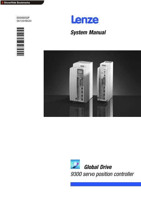
EDSVS9332P!.ðv7Ä!."v7äLSystem ManualGlobal Drive9300 servo position controller
PartProjectplanningA ContentsPreface and general information•Safety informationB Technical data •<strong>Installation</strong>C CommissioningContent of the 9300 System ManualsServoinverterServo positioncontrollerServocam profilerServo registercontroller• • • •• • • •• • • •During operation • •• •User Manual ”Oscilloscope function”D Configuration D1.1 D2.1 D3.1 D4.1Code table D1.2 D2.2 D3.2 D4.2e Troubleshooting and fault elimination • • • •f DC-bus operationOperating Instructions for 9340 regenerative •power supply moduleGHApplication of brake unitsOperating Instructions for 9350 brake unitAutomationAutomation with system bus (CAN)••Operating Instructions for 2102 fieldbusmodule (RS232/RS485)•Operating Instructions for 2111 fieldbusmodule (INTERBUS)•Operating Instructions for 2131 fieldbusmodule (PROFIBUS)•Flyer PC software Global Drive Control•I Accessories and motors •K How to select the correct driveApplication examples • • • •L Signal flow diagrams • • • •M GlossaryTable of keywords• • • • •• part of the corresponding System ManualAll documentation listed here contains a type designation and an identification code at the top left edge.The features and data of the controller specified in your System Manual correspond to the controller version at the time of printing (date of printing: seeinner cover page of the parts).Lenze strives to keep all information to the state of the latest controller version. If you should still find deviations from your System Manual, we kindlyask you to refer to the Operating Instructions included in the scope of supply or to contact your Lenze representative directly.
$%%"!5 D EA @ I D A A J B = E I ? A ? JE ! 7 / 7 / = E I ? A ? JE = @ , + ? A ? JE 2 -4 , ; 1 2 1 = N = N . = E # HF + 6 4 ) + 6, A J= ? D = > A F A H = JE C @ K A= JA H = JEL A O. EA @ > K I A I1 6 - 4 * 7 5: : D E@ @ A ) K J = JE E JA H B= ? A: "/ , 0 15 O I JA > K I + ) : #: $! ' - # - " - ! - - &# ' 5 6 ) ! ) ) $ ! ) "5 6+ JH JA H E = I: %#4 A I L A H E F K J: &#- ? @ A H E F K J: '#, EC EJ= BH A G K A ? O E F K J5 D EA @ ? A ? JE : #, EC EJ= BH A G K A ? O K JF K J7 8 96 62 6 +2 -5 D EA @ I D A A J B? JH ? A ? JE I2 6 + ? A ? JE J H ? A ? JE 5 D EA @ I D A A J B J H ? = > A IK35.0002
EDSVS9332P-ALSystem ManualPart AContentsPreface and general informationGlobal Drive9300 servo position controller
This documentation is valid for 9300 position controllers as of version:33.932X EP 2x 2x (9321 - 9329)33.933X EP 2x 2x (9330 - 9332)33.932X CP 2x 2x - V003 Cold Plate (9321 - 9328)TypeDesign:EP = Built-in unit IP20CP = Cold PlateHardware version and indexSoftware version and indexVariantExplanation© 2004 Lenze Drive Systems GmbH, HamelnNo part of these Instructions must be copied or given to third parties without written approval of Lenze Drive Systems GmbH.All indications given in this documentation have been selected carefully and comply with the hardware and software described.Nevertheless, deviations cannot be ruled out. We do not take any responsibility or liability for damages which might possibly occur. Necessarycorrections will be included in the next edition.3.0 11/2004
ContentsPart A1 Preface and general information ........................................... 1-11.1 How to use this Manual ............................................................1-11.1.1 Terminology used .........................................................1-11.1.2 What is new? ............................................................1-11.2 Legal regulations .................................................................1-21.3 EC directives / Declaration of conformity ................................................1-31.3.1 What is the purpose of EC directives? ...........................................1-31.3.2 What does the CE marking imply? .............................................1-31.3.3 EC Low-Voltage Directive ....................................................1-41.3.3.1 General .......................................................1-41.3.4 EC Directive Electromagnetic Compatibility .......................................1-51.3.4.1 General .......................................................1-51.3.5 EC Machinery Directive .....................................................1-71.3.5.1 General .......................................................1-72 Safety instructions ...................................................... 2-12.1 General safety and application notes for Lenze controllers ...................................2-12.2 Residual hazards .................................................................2-32.3 Layout of the safety instructions ......................................................2-3L EDSVS9332P-A EN 3.0i
ContentsPart B3 Technical data ......................................................... 3-13.1 Features .......................................................................3-13.2 General data/operating conditions ....................................................3-23.3 Rated data ......................................................................3-33.3.1 Types 9321 to 9325 ........................................................3-33.3.2 Types 9321 to 9324 with 200 % overcurrent .....................................3-43.3.3 Types 9326 to 9332 ........................................................3-53.3.4 Fuses and cable cross-sections ...............................................3-63.3.5 Mains filter ..............................................................3-73.4 Dimensions .....................................................................3-74 <strong>Installation</strong> ............................................................ 4-14.1 Mechanical installation .............................................................4-14.1.1 Important notes ...........................................................4-14.1.2 Standard assembly with fixing rails or fixing brackets ...............................4-24.1.3 Assembly with thermally separated power stage (”Push-through technique”) ..............4-34.1.4 Assembly of variants .......................................................4-64.2 Electrical installation ..............................................................4-94.2.1 Protection of persons .......................................................4-94.2.1.1 Residual-current circuit breakers ....................................4-94.2.1.2 Isolation ....................................................... 4-104.2.1.3 Replacement of defective fuses ..................................... 4-104.2.1.4 Mains disconnection .............................................. 4-104.2.2 Protection of the controller ................................................... 4-114.2.3 Motor protection .......................................................... 4-114.2.4 Mains types/mains conditions ................................................ 4-114.2.5 Interaction with compensation equipment ........................................ 4-124.2.6 Specification of the cables used ............................................... 4-124.2.7 Power connections ........................................................ 4-124.2.7.1 Mains connection ................................................ 4-134.2.7.2 Motor connection ................................................ 4-164.2.7.3 Connection of a brake unit ......................................... 4-214.2.7.4 DC bus connection of several drives .................................. 4-224.2.8 Control connections ........................................................ 4-244.2.8.1 Control cables .................................................. 4-244.2.8.2 Assignment of the control terminals .................................. 4-244.2.8.3 Connection of digital signals (X5) .................................... 4-254.2.8.4 Connection of analog signals (X6) .................................... 4-284.2.9 Automation interface (X1) .................................................... 4-344.2.10 Motor temperature monitoring ................................................ 4-354.2.10.1 User-specific characteristic for a PTC thermistor ......................... 4-364.2.11 Feedback systems ......................................................... 4-374.3 <strong>Installation</strong> of a CE-typical drive system ................................................ 4-41iiEDSVS9332P-A EN 3.0L
ContentsPart C5 Commissioning ........................................................ 5-15.1 Before switching on ...............................................................5-15.2 Initial switch-on ..................................................................5-15.3 Commissioning sequence ...........................................................5-45.4 Switchoncontroller ...............................................................5-55.5 SwitchonPC,startGDC ............................................................5-65.6 Generate parameter set ............................................................5-75.6.1 Adapt controller to the mains .................................................5-75.6.2 Adapt controller to the motor .................................................5-85.6.3 Enter machine parameters ...................................................5-95.6.4 Parameters for manual control ................................................ 5-105.6.5 Controller enable .......................................................... 5-115.7 Function test with manual control ..................................................... 5-125.8 Enter travel profile parameters ....................................................... 5-145.8.1 Structure of a positioning program ............................................. 5-145.8.1.1 Tools for editing ................................................. 5-155.8.1.2 Structure of a travel profile ......................................... 5-165.8.1.3 Enter parameter ................................................. 5-205.8.2 Saving a parameter set ..................................................... 5-215.9 Load parameter set ............................................................... 5-225.9.1 Load parameter set from the PC ............................................... 5-225.9.2 Load parameter set from the controller .......................................... 5-235.10 Control drive .................................................................... 5-245.10.1 Description of the dialog box ................................................. 5-245.10.2 Parameters for homing ..................................................... 5-255.10.3 Manual homing ........................................................... 5-265.10.4 Program control ........................................................... 5-275.11 Automatic control parameter identification .............................................. 5-285.11.1 Procedure ............................................................... 5-295.11.2 Troubleshooting ........................................................... 5-305.11.2.1 Password protection .............................................. 5-316 During operation ....................................................... 6-16.1 Status indications ................................................................6-16.1.1 Display on the controller ....................................................6-16.1.2 Display on the keypad ......................................................6-16.1.3 Display in Global Drive Control ................................................6-26.1.4 Actual value display via codes ................................................6-36.2 Information on operation ...........................................................6-36.2.1 Switching on the motor side ..................................................6-36.2.2 Controller protection by current derating .........................................6-4L EDSVS9332P-A EN 3.0iii
ContentsPart D2.17 Configuration .......................................................... 7-17.1 Configuration with Global Drive Control .................................................7-17.1.1 Changing the basic configuration ..............................................7-27.2 Operating modes .................................................................7-37.2.1 Parameter setting .........................................................7-37.2.2 Control .................................................................7-37.2.3 Signal types .............................................................7-47.2.4 Elements of a function block .................................................7-57.2.5 Connection of function blocks ................................................7-77.2.6 Entries into the processing table .............................................. 7-117.2.6.1 Signal configuration with Global Drive Control ........................... 7-137.3 Terminal assignment .............................................................. 7-147.3.1 Freely assignable digital inputs ............................................... 7-157.3.2 Freely assignable digital outputs .............................................. 7-167.3.3 Input and outputof the STATE-BUS ............................................. 7-177.3.4 Freely assignable analog inputs ............................................... 7-187.3.5 Freely assignable analog outputs .............................................. 7-197.4 Description of the function blocks ..................................................... 7-207.5 Positioning control (POS) ........................................................... 7-247.5.1 Dimensions .............................................................. 7-307.5.2 Machine parameters ....................................................... 7-317.5.2.1 Position encoder at material path .................................... 7-337.5.3 Positioning modes (C1210) ................................................... 7-357.5.3.1 Relative positioning .............................................. 7-357.5.3.2 Absolute positioning .............................................. 7-377.5.3.3 Absolute positioning with saving ..................................... 7-387.5.4 Measuring systems ........................................................ 7-397.5.4.1 Measuring systems and zero shifts ................................... 7-407.5.4.2 Measuring systems for absolute value encoders ......................... 7-417.5.5 Absolute value encoder ..................................................... 7-427.5.5.1 Absolute value encoder via encoder connection X8 ....................... 7-427.5.5.2 Absolute value encoder via system bus (CAN) ........................... 7-447.5.6 Control structure .......................................................... 7-467.5.7 Travel range limits ......................................................... 7-477.5.7.1 End of travel range limit switch ...................................... 7-477.5.7.2 Position limit values (C1223, C1224) .................................. 7-487.5.8 Homing ................................................................. 7-497.5.8.1 Homing ....................................................... 7-497.5.8.2 Homing end .................................................... 7-507.5.8.3 Referencing status (POS-REF-OK) .................................... 7-517.5.8.4 Homing mode 0 and 1 ............................................ 7-527.5.8.5 Homing mode 2 and 3 ............................................ 7-537.5.8.6 Homing mode 4 and 5 ............................................ 7-547.5.8.7 Homing mode 6 and 7 ............................................ 7-557.5.8.8 Homing mode 8 and 9 ............................................ 7-567.5.8.9 Homing mode 10 and 11 .......................................... 7-577.5.8.10 Second homing speed ............................................ 7-587.5.8.11 Set homing value ................................................ 7-58ivEDSVS9332P-A EN 3.0L
Contents7.5.9 Travel profile generator and setpoints ........................................... 7-597.5.9.1 Linear ramps (L profile) ........................................... 7-607.5.9.2 S ramps (S profile) ............................................... 7-617.5.9.3 Override ....................................................... 7-637.5.9.4 New travel profile parameters during positioning ......................... 7-637.5.9.5 Influence of precontrol values (POS-NOUT-GAIN, POS-MOUT-GAIN) ............ 7-637.5.9.6 ”Target-reached” message (POS-IN-TARGET) ............................ 7-647.5.9.7 Target window (POS-WAITSTATE) ..................................... 7-657.5.9.8 Virtual master (output POS-PHI-SET) .................................. 7-667.5.9.9 Setting the actual position value (POS-ABS-SET) ......................... 7-677.5.10 Manual operation ......................................................... 7-687.5.10.1 Manual positioning ............................................... 7-697.5.10.2 Manual positioning with intermediate stop .............................. 7-707.5.10.3 Manual homing ................................................. 7-707.5.11 Program operation ......................................................... 7-717.5.11.1 Program control ................................................. 7-717.5.11.2 Status of the program control ....................................... 7-737.5.12 Variable tables (VT) ........................................................ 7-757.5.13 Program sets (PS) ......................................................... 7-767.5.13.1 PS mode ...................................................... 7-777.5.13.2 Point-to-point positioning .......................................... 7-787.5.13.3 Point-to-point positioning with changeover of velocity ..................... 7-797.5.13.4 Touch probe positioning ........................................... 7-807.5.13.5 Stand-by mode ................................................. 7-817.5.13.6 Set position value ................................................ 7-847.5.13.7 Prg. fct. “Wait for input” ........................................... 7-857.5.13.8 Prg. fct. “Switch output before positioning” ............................. 7-857.5.13.9 Prg. fct. “Switch output after positioning” .............................. 7-867.5.13.10 Prg. fct. “Waiting time” ............................................ 7-867.5.13.11 Prg. fct. “Branch 1” .............................................. 7-877.5.13.12 Prg. fct. “Branch 2” .............................................. 7-877.5.13.13 Prg. fct. “Repetition function - No. of pieces” ........................... 7-887.5.13.14 Prg fct. “Jump to next PS” ......................................... 7-897.5.14 POS-TP (Touch-probe saving of the actual position value) ............................ 7-907.5.15 POS-PFI (Program Function Inputs) ............................................. 7-927.5.16 POS-PFO (Program Function Outputs) ........................................... 7-937.5.17 Absolute value generator (ABS) ............................................... 7-947.5.18 Addition block (ADD) ....................................................... 7-957.5.19 Automation interface (AIF-IN) ................................................. 7-967.5.20 Automation interface (AIF-OUT) ............................................... 7-997.5.21 Analog input via terminal 1,2/3,4 (AIN) .......................................... 7-1017.5.22 AND operation (AND) ....................................................... 7-1037.5.23 Inverter (ANEG) ........................................................... 7-1067.5.24 Analog output via terminal 62/63 (AOUT) ........................................ 7-1077.5.25 Arithmetic block (ARIT) ..................................................... 7-1097.5.26 Arithmetic block (ARITPH) ................................................... 7-1107.5.27 Changeover switch for analog signals (ASW) ...................................... 7-1137.5.28 BCD decade switch (BCD) ................................................... 7-1157.5.28.1 Data inputs .................................................... 7-1197.5.28.2 Signal processing ................................................ 7-1207.5.28.3 ”CANCEL” function ............................................... 7-1217.5.28.4 ”RESET” function ................................................ 7-1217.5.28.5 BCD decade switch .............................................. 7-1227.5.28.6 Complete BCD reading ............................................ 7-1237.5.28.7 BCD mode ..................................................... 7-124L EDSVS9332P-A EN 3.0v
Contents7.5.29 Holding brake (BRK) ........................................................ 7-1267.5.29.1 Applying the brake ............................................... 7-1277.5.29.2 Opening the brake (release) ........................................ 7-1287.5.29.3 Setting controller inhibit ........................................... 7-1297.5.30 System bus (CAN-IN) ....................................................... 7-1317.5.31 System bus (CAN-OUT) ..................................................... 7-1387.5.32 Comparator (CMP) ......................................................... 7-1437.5.32.1 Function 1: CMP1-IN1 = CMP1-IN2 ................................... 7-1447.5.32.2 Function 2: CMP1-IN1 > CMP1-IN2 ................................... 7-1457.5.32.3 Function 3: CMP1-IN1 < CMP1-IN2 ................................... 7-1457.5.32.4 Function 4: |CMP1-IN1| = |CMP1-IN2| ................................. 7-1467.5.32.5 Function 5: |CMP1-IN1| > |CMP1-IN2| ................................. 7-1467.5.32.6 Function 6: |CMP1-IN1| < |CMP1-IN2| ................................. 7-1467.5.33 Long comparator (CMPPH) ................................................... 7-1477.5.33.1 Function 1: CMPPH1-IN1 = CMPPH1-IN2 ............................... 7-1497.5.33.2 Function 2: CMPPH1-IN1 > CMPPH1-IN2 ............................... 7-1507.5.33.3 Function 3: CMPPH1-IN1 < CMPPH1-IN2 ............................... 7-1507.5.33.4 Function 4: |CMPPH1-IN1| = |CMPPH1-IN2| ............................. 7-1517.5.33.5 Function 5: |CMPPH1-IN1| > |CMPPH1-IN2| ............................. 7-1517.5.33.6 Function 6: |CMPPH1-IN1| < |CMPPH1-IN2| ............................. 7-1517.5.34 Signal conversion (CONV) .................................................... 7-1527.5.35 Analog-digital converter (CONVAD) ............................................. 7-1557.5.36 Analog-phase converter (CONVAPH) ............................................ 7-1577.5.37 Digital-analog converter (CONVDA) ............................................. 7-1597.5.38 Phase-analog converter (CONVPHA) ............................................ 7-1627.5.39 Phase conversion (CONVPHPH2) ............................................... 7-1647.5.40 Characteristic function (CURVE) ............................................... 7-1657.5.40.1 Characteristic with two co-ordinates .................................. 7-1667.5.40.2 Characteristic with three co-ordinates ................................. 7-1667.5.40.3 Characteristic with four co-ordinates .................................. 7-1677.5.41 Dead band (DB) ........................................................... 7-1687.5.42 Controller control (DCTRL) ................................................... 7-1697.5.42.1 Quick stop (QSP) ................................................ 7-1707.5.42.2 Operation inhibited (DISABLE) ....................................... 7-1707.5.42.3 Controller inhibit (CINH) ........................................... 7-1707.5.42.4 TRIP-SET ...................................................... 7-1717.5.42.5 TRIP-RESET .................................................... 7-1717.5.42.6 Controller status ................................................. 7-1717.5.43 Digital frequency input (DFIN) ................................................. 7-1727.5.44 Digital frequency output (DFOUT) .............................................. 7-1757.5.44.1 Output signals to X10 ............................................. 7-1767.5.44.2 Output of an analog signal ......................................... 7-1777.5.44.3 Output of a speed signal ........................................... 7-1777.5.44.4 Encoder simulation of the resolver ................................... 7-1787.5.44.5 Direct output of X8 (C0540 = 5) ..................................... 7-1787.5.44.6 Direct output of X9 (C0540 = 4) ..................................... 7-1787.5.45 Digital frequency ramp function generator (DFRFG) ................................. 7-1797.5.45.1 Profile generator ................................................ 7-1807.5.45.2 Quick stop ..................................................... 7-1817.5.45.3 Ramp function generator stop ....................................... 7-1817.5.45.4 RESET ........................................................ 7-1827.5.45.5 Detect phase difference ........................................... 7-1827.5.45.6 Start via touch probe initiator (terminal X5/E5) ........................... 7-1837.5.45.7 Correction of the touch probe initiator (terminal X5/E5) .................... 7-1847.5.45.8 Offset setting ................................................... 7-184viEDSVS9332P-A EN 3.0L
Contents7.5.46 Digital frequency processing (DFSET) ........................................... 7-1857.5.46.1 Setpoint conditioning with stretching and gearbox factor ................... 7-1867.5.46.2 Processing of correction values ...................................... 7-1877.5.46.3 Synchronising to zero track or touch probe ............................. 7-1887.5.47 Delay elements (DIGDEL) .................................................... 7-1897.5.47.1 On-delay ...................................................... 7-1907.5.47.2 Dropout delay ................................................... 7-1907.5.47.3 General delay ................................................... 7-1917.5.48 Freely assignable digital inputs (DIGIN) .......................................... 7-1927.5.49 Freely assignable digital outputs (DIGOUT) ....................................... 7-1937.5.50 Free analog display code (DISA) ............................................... 7-1947.5.51 Free phase display code (DISPH) .............................................. 7-1967.5.52 First order derivative-action element (DT1) ....................................... 7-1977.5.53 Free piece counter (FCNT) ................................................... 7-1987.5.54 Free codes (FCODE) ........................................................ 7-2017.5.55 Free digital outputs (FDO) .................................................... 7-2027.5.56 Freely assignable input variables (FEVAN) ........................................ 7-2047.5.57 Fixed setpoints (FIXSET) ..................................................... 7-2117.5.57.1 Enabling of the FIXSET1 setpoints .................................... 7-2127.5.58 Flipflop element (FLIP) ...................................................... 7-2137.5.59 Limiter (LIM) ............................................................. 7-2167.5.60 Internal motor control (MCTRL) ................................................ 7-2177.5.60.1 Current controller ................................................ 7-2197.5.60.2 Additional torque setpoint .......................................... 7-2197.5.60.3 Torque limitation ................................................ 7-2207.5.60.4 Speed controller ................................................. 7-2217.5.60.5 Torque control with speed limitation .................................. 7-2227.5.60.6 Speed setpoint limitation .......................................... 7-2227.5.60.7 Phase controller ................................................. 7-2237.5.60.8 Quick stop QSP ................................................. 7-2247.5.60.9 Field weakening ................................................. 7-2257.5.60.10 Switching frequency changeover ..................................... 7-2257.5.61 Motor phase failure detection (MLP) ............................................ 7-2267.5.62 Monitor outputs of monitoring system (MONIT) .................................... 7-2277.5.63 Motor potentiometer (MPOT) ................................................. 7-2287.5.64 Logic NOT ............................................................... 7-2317.5.65 Speed setpoint conditioning (NSET) ............................................ 7-2337.5.65.1 Main setpoint path ............................................... 7-2347.5.65.2 JOG setpoints ................................................... 7-2357.5.65.3 Setpoint inversion ................................................ 7-2367.5.65.4 S ramp ....................................................... 7-2377.5.65.5 Arithmetic operation .............................................. 7-2377.5.65.6 Additional setpoint ............................................... 7-2387.5.66 OR operation (OR) ......................................................... 7-2397.5.67 Oscilloscope function (OSZ) .................................................. 7-2427.5.68 Process controller (PCTRL1) .................................................. 7-2467.5.68.1 Control characteristic ............................................. 7-2477.5.68.2 Ramp function generator .......................................... 7-2487.5.68.3 Value range of the output signal ..................................... 7-2487.5.68.4 Evaluation of the output signal ...................................... 7-2487.5.68.5 Deactivation of the process controller ................................. 7-2487.5.69 Signal adaptation for phase signals (PHDIV) ...................................... 7-2497.5.70 Phase integrator (PHINT) .................................................... 7-2507.5.70.1 Constant input value .............................................. 7-2517.5.70.2 Scaling of PHINTx-OUT ............................................ 7-252L EDSVS9332P-A EN 3.0vii
Contents7.5.71 First order delay element (PT1) ................................................ 7-2537.5.72 CW/CCW-QSP link (R/L/Q) ................................................... 7-2547.5.73 Ramp function generator (RFG) ............................................... 7-2557.5.73.1 Calculation and setting of the times Tir and Tif .......................... 7-2567.5.73.2 Loading of the ramp function generator ................................ 7-2567.5.74 Sample and hold function (S&H) ............................................... 7-2577.5.75 Phase value selection (SELPH) ................................................ 7-2587.5.76 Switching points (SP) ....................................................... 7-2607.5.76.1 Switching points ................................................. 7-2627.5.76.2 Hysteresis ..................................................... 7-2637.5.76.3 Dead time ..................................................... 7-2647.5.76.4 Filter time constant .............................................. 7-2657.5.77 Output of digital status signals (STAT) ........................................... 7-2667.5.78 Control of a drive network (STATE-BUS) ......................................... 7-2677.5.79 Multi-axis synchronisation (SYNC1) ............................................ 7-2687.5.79.1 Possible axis synchronisations ...................................... 7-2697.5.79.2 Cycle times .................................................... 7-2717.5.79.3 Phase displacement .............................................. 7-2737.5.79.4 Time slot for synchronisation via terminal .............................. 7-2737.5.79.5 Correction value of the phase controller ............................... 7-2747.5.79.6 Fault indications ................................................. 7-2747.5.79.7 Configuration examples ........................................... 7-2757.5.79.8 Scaling ....................................................... 7-2757.5.80 Teach-in in programming (TEACH) ............................................. 7-2767.5.81 Edge evaluation (TRANS) .................................................... 7-2787.5.81.1 Evaluate positive edge ............................................ 7-2797.5.81.2 Evalute negative edge ............................................ 7-2797.5.81.3 Evaluate positive or negative edge ................................... 7-2807.5.82 Variable table - acceleration (VTACC) ........................................... 7-2817.5.83 Variable table Piece number (VTPCS) ........................................... 7-2837.5.84 Variable table - target position/position values (VTPOS) .............................. 7-2857.5.85 Variable table Waiting time (VTTIME) ............................................ 7-2877.5.86 Variable table - speed (VTVEL) ................................................ 7-289viiiEDSVS9332P-A EN 3.0L
Contents7.6 Monitoring ...................................................................... 7-2917.6.1 Reactions ............................................................... 7-2917.6.2 Set reactions ............................................................. 7-2927.6.3 Monitoring functions ....................................................... 7-2937.6.3.1 System fault CCr ................................................ 7-2957.6.3.2 Communication error CE0 .......................................... 7-2967.6.3.3 External error EEr ............................................... 7-2977.6.3.4 Power stage identification H07 ...................................... 7-2987.6.3.5 Monitoring for failure of a motor phase LP1 ............................. 7-2997.6.3.6 Low voltage LU ................................................. 7-3007.6.3.7 System speed monitoring NMax ..................................... 7-3017.6.3.8 Monitoring for short-circuit OC1 ..................................... 7-3027.6.3.9 Monitoring for earth fault OC2 ....................................... 7-3037.6.3.10 Fault message (OC5) ............................................. 7-3047.6.3.11 Heatsink monitoring OH (fixed) ...................................... 7-3057.6.3.12 Motor temperature monitoring OH3 (fixed) ............................. 7-3067.6.3.13 Heatsink monitoring OH4 (adjustable) ................................. 7-3077.6.3.14 Motor temperature monitoring OH7 (adjustable) .......................... 7-3087.6.3.15 Motor temperature monitoring OH8 ................................... 7-3097.6.3.16 Overvoltage OU ................................................. 7-3107.6.3.17 Following error P03 .............................................. 7-3127.6.3.18 Phase controller overflow P13 ....................................... 7-3137.6.3.19 Parameter error PRO .............................................. 7-3147.6.3.20 Parameter set error PR1, PR2, PR3, PR4 ............................... 7-3157.6.3.21 Resolver monitoring for wire breakage Sd2 ............................. 7-3167.6.3.22 Dig-Set monitoring Sd3 ........................................... 7-3177.6.4 Fault indication via digital output .............................................. 7-3187.7 Parameter setting ................................................................. 7-3197.7.1 Possible parameter settings .................................................. 7-3197.7.2 Structure of a parameter set ................................................. 7-320Part D2.27.8 Code table ...................................................................... 7-3237.9 Selection lists ................................................................... 7-3817.9.1 Selection list - signal links ................................................... 7-3817.9.2 Table of attributes ......................................................... 7-3897.9.3 Motor selection list ........................................................ 7-4067.9.3.1 Servo motors ................................................... 7-4067.9.3.2 Three-phase AC asynchronous motor ................................. 7-409L EDSVS9332P-A EN 3.0ix
ContentsPart E8 Troubleshooting and fault elimination ...................................... 8-18.1 Troubleshooting ..................................................................8-18.2 Error analysis with the history buffer ...................................................8-38.2.1 Structure of the history buffer ................................................8-38.2.2 Working with the history buffer ...............................................8-48.3 Fault messages ..................................................................8-58.4 Reset of fault messages ............................................................ 8-10Part F9 Network of several drivesSee folder “Planning”Part G10 Application of brake unitsSee folder “Planning”Part H11 AutomationSee folder “Planning”Part I12 Accessories and motorsSee folder “Planning”Part K13 Selection helpSee folder “Planning”14 Application examples ................................................... 14-114.1 Example 1: Dosing ................................................................ 14-114.2 Example 2: Spray jet control ......................................................... 14-514.3 Example 3: Contouring control ....................................................... 14-814.3.1 Commissioning of the contouring control ........................................ 14-11Part L15 Signal flow diagram .................................................... 15-1Part M16 Glossary .............................................................. 16-117 Table of keywords ...................................................... 17-1xEDSVS9332P-A EN 3.0L
Preface and general informationPart A1 Preface and general information1.1 How to use this Manual• This Manual supplements the Operating Instructions of the servo position controller 93XX.• It contains the Operating Instructions which were valid at the time of printing of the SystemManual and additional information on systems engineering, functionality and accessories.– In case of doubt, the Operating Instructions attached to the 93XX servo position controlleris valid.• The System Manual helps to select and dimension the 93XX servo position controller andaccessories to ensure a safe and trouble-free operation. It contains safety information whichmust be observed.• The System Manual must always be in a complete and perfectly readable state.1.1.1 Terminology usedTermIn the following text used for93XX Any type of servo position controller (types 9321 ... 9332)Controller93XX servo position controllerDrive systemDrive systems with servo position controllers 93XX and otherLenze drive components1.1.2 What is new?Version Id. No. Modifications1.0 05/97 00397653 First edition2.0 02/99 00406175 Types 9321 to 9324 with 200% overcurrent, new function “Automatic control parameteridentification”3.0 03/2003 TD23 00463261 Fault correction and editorial revisionl EDSVS9332P-A EN 3.01-1
Preface and general information1.2 Legal regulationsLabelling Nameplate CE-identification ManufacturerLenze controllers are unambiguouslydesignated by the contents of the nameplate.Conforms to the EC Low-Voltage DirectiveLenze Drive Systems GmbHPostfach 101352D-31763 HamelnApplication as 93XX servo position controllerdirected • must only be operated under the conditions prescribed in these Instructions.• are components– for open and closed loop control of variable speed drives with PM synchronous motors, asynchronous servo motors or asynchronousstandard motors.– for installation in a machine– for assembly with other components to form a machine.• are electric units for the installation into control cabinets or similar enclosed operating housing.• comply with the requirements of the Low-Voltage Directive.• are not machines for the purpose of the Machinery Directive.• are not to be used as domestic appliances, but for industrial purposes only.Drive systems with 93XX servo position controllers• comply with the EMC Directive if they are installed according to the guidelines of CE-typical drive systems.• can be used– for operation on public and non-public mains– for operation in industrial premises and residential areas.• The user is responsible for the compliance of his application with the EC directives.Any other use shall be deemed inappropriate!Liability • The information, data, and notes in these Instructions met the state of the art at the time of printing. Claims on modifications referring tocontrollers which have already been supplied cannot be derived from the information, illustrations, and descriptions.• The specifications, processes, and circuitry described in these Instructions are for guidance only and must be adapted to your own specificapplication. Lenze does not take responsibility for the suitability of the process and circuit proposals.• The specifications in these Instructions describe the product features without guaranteeing them.• Lenze does not accept any liability for damage and operating interference caused by:– disregarding the Operating Instructions– unauthorised modifications to the controller– operating errors– improper working on and with the controllerWarranty • Terms of warranty: see terms of sales and delivery of Lenze Drive Systems GmbH.• Warranty claims must be made to Lenze immediately after detecting the deficiency or fault.• The warranty is void in all cases where liability claims cannot be made.Disposal Material recycle disposeMetal D -Plastic D -Assembled PCBs - D1-2 EDSVS9332P-A EN 3.0l
Preface and general information1.3 EC directives / Declaration of conformity1.3.1 What is the purpose of EC directives?The EC directives are issued by the European Council and are intended for the determination ofcommon technical requirements (harmonisation) and certification procedures with the EuropeanCommunity. At the moment, there are 21 EC directives for product ranges. The directives are or willbe converted into national laws of the member states. A certification issued by one member stateis valid automatically without any further approval in all other member states.The texts of the directives are restricted to the essential requirements. Technical details are or willbe determined by European harmonised standards.1.3.2 What does the CE marking imply?After a verification, the conformity according to the EC directives is certified by affixing a CEmarking.WithintheECtherearenocommercialbarriersforaproductprovidedwithaCEmarking.Attaching a declaration of conformity is not necessary for most of the directives. Users or customersare therefore not aware which of the 21 EC Directives comply with a certain product and whichharmonised standards were considered in the evaluation procedure of conformity.Controllers with the CE marking exclusively correspond to the Low Voltage Directive. So far, onlyrecommendations were given for the compliance with the EMC regulation. In this case, the userhimself has to prove the compliance with the CE directives for the installation of a machine. Lenzehas already provided evidence of installing CE-typical drive systems and confirmed this by thedeclaration of conformity to the EMC EC directive.l EDSVS9332P-A EN 3.01-3
Preface and general information1.3.3 EC Low-Voltage Directive(73/23/EEC)amended by:CE-mark Directive (93/68/EWG)1.3.3.1 General• The Low-Voltage Directive applies to all electrical equipment for use with a rated voltagebetween 50 V and 1000 V AC and between 75 and 1500 V DC under normal ambientconditions, except for e.g. the use of electrical equipment in explosive atmospheres andelectrical parts in passenger and goods lifts.• The objective of the Low-Voltage Directive is to ensure that only such electrical equipment isplaced on the market which does neither endanger the safety of persons and animals nor theconservation of material assets.9300std0011-4 EDSVS9332P-A EN 3.0l
Preface and general information1.3.4 EC Directive Electromagnetic Compatibility(89/336/EWG)amended by:1st Amendment Directive (92/31/EWG)CE-marking Directive (93/68/EWG)1.3.4.1 General• The EC Directive ”Electromagnetic Compatibility” applies to ”devices” which may causeelectromagnetic interferences or the operation of which may be impaired by suchinterferences.• The aim is to limit the generation of electromagnetic interferences such that radio andtelecommunication systems and other equipment can be operated without interferences.Furthermore the devices must show an appropriate resistance against electromagneticinterference to ensure the application as directed.• Controllers cannot be operated on their own. Controllers cannot be evaluated on their own interms of EMC. Only when being integrated into a drive system the compliance with theobjectives of the EC Directive ”EMC” and the observance of the ”Law on electromagneticcompatibility of devices” canbechecked.• Lenze has evaluated the conformity of the controllers in defined drive systems. In thefollowing, these evaluated drive systems are called ”CE-typical drive system”.Therefore the user of the controllers can– either determine the system components and their integration into a drive system anddeclare the conformity on his own responsibility,– or install the drive system according to the CE-typical drive system evaluated by theinverter manufacturer who already proved the conformity.Components of the CE-typical drive systemSystem componentControllerMains filter A/BMotor cableMains cable between mains filterand controllerControl cablesMotorSpecificationController types 93XX seriesFor type designation see first cover pageFor data and filter assignment see chapter ”Ratings”Shielded power cable with tinned E-CU braid with a minimum of 85% optical coverage.From a minimum cable length of 300 mm:Shielded power cable with tinned E-CU braid with a minimum of 85% optical coverage.Shielded signal cable type LIYCYStandard three-phase asynchronous motor, servo synchronous motor, servo asynchronous motorLenze types DXRA, MDXKX or similar• Controller, FFI filter and mains choke are located on a common mounting plate.• The system components have been wired according to chapter 4 ”Electrical installation”.l EDSVS9332P-A EN 3.01-5
Preface and general information9300std0021-6 EDSVS9332P-A EN 3.0l
Preface and general information1.3.5 EC Machinery Directive(98/37/EC)1.3.5.1 GeneralFor the purpose of the Machinery Directive, ”machinery” means an assembly of linked parts orcomponents, at least one of which moves, with the appropriate actuators, control and powercircuits, etc., joined together for a specific application, in particular for processing, treatment,moving or packaging of a material.9300std003l EDSVS9332P-A EN 3.01-7
Preface and general information1-8 EDSVS9332P-A EN 3.0l
Safety instructions2 Safety instructions2.1 General safety and application notes for Lenze controllers(to: Low-Voltage Directive 73/23/EEC)GeneralLenze controllers (frequency inverters, servo inverters, DC controllers) can include live and rotatingparts - depending on their type of protection - during operation. Surfaces can be hot.Non-authorized removal of the required cover, inappropriate use, incorrect installation or operation,creates the risk of severe injury to persons or damage to material assets.For more detailed information please see the documentation.All operations concerning transport, installation, and commissioning as well as maintenance mustbe carried out by qualified, skilled personnel (IEC 364 or CENELEC HD 384 or DIN VDE 0100 andIEC report 664 or DIN VDE 0110 and national regulations for the prevention of accidents must beobserved).According to this basic safety information qualified skilled personnel are persons who are familiarwith the installation, assembly, commissioning, and operation of the product and who have thequalifications necessary for their occupation.Application as directedDrive controllers are components which are designed for installation in electrical systems ormachinery. They are not to be used as household appliances. They are intended exclusively forprofessional and commercial purposes according to EN 61000-3-2. This documentation includesinformation about the compliance with the limit values to EN 61000-3-2.When installing the drive controllers in machines, commissioning (i.e. starting of operation asdirected) is prohibited until it is proven that the machine complies with the regulations of the ECDirective 98/37/EC (Machinery Directive); EN 60204 must be observed.Commissioning (i.e. starting of operation as directed)is only allowed when there is compliance withtheEMCDirective(89/336/EEC).The drive controllers meet the requirements of the Low-Voltage Directive 73/23/EEC. Theharmonised standards of the series EN 50178/DIN VDE 0160 apply to the controllers.The technical data and information on the connection conditions must be obtained from thenameplate and the documentation. They must be observed in any case.Warning: The availability of controllers is restricted according to EN 61800-3. These products cancause radio interferences in residential areas. In this case, special measures are required.Transport, storagePlease observe the notes on transport, storage and appropriate handling.Observe the climatic conditions according to EN 50178.<strong>Installation</strong>The controllers must be installed and cooled according to the regulations given in thedocumentation.Ensure proper handling and avoid mechanical stress. Do not bend any components and do notchange any insulation distances during transport or handling. Do not touch any electroniccomponents and contacts.Controllers contain electrostatically sensitive components which can easily be damaged byinappropriate handling. Do not damage or destroy any electrical components since this mightendanger your health!L EDSVS9332P-A EN 3.02-1
Safety instructionsElectrical connectionWhen working on live drive controllers, the applicable national regulations for the prevention ofaccidents (e.g. VBG 4) must be observed.The electrical installation must be carried out according to the appropriate regulations (e.g. cablecross-sections, fuses, PE connection). Additional information can be obtained from thedocumentation.The documentation contains information about installation in compliance with EMC (shielding,earthing, filters and cables). These notes must also be observed for CE-marked controllers. Themanufacturer of the system or machine is responsible for the compliance with the required limitvalues demanded by the EMC legislation.OperationIf necessary, systems including controllers must be equipped with additional monitoring andprotection devices according to the corresponding standards (e.g. law on technical equipment,regulations for the prevention of accidents, etc.). If necessary, adapt the controllers to yourapplication. Please observe the corresponding information given in the Instructions.After the controller has been disconnected from the supply voltage, live components and powerconnection must not be touched immediately since capacitors could be charged. Please observethe corresponding notes on the controller.All covers and doors must be closed during operation.Note for UL-approved systems with integrated controllers: UL warnings are notes which applyto UL systems. The documentation contains special information about UL.Safe standstill -1-Variant V004 of the controller series 9300 and 9300 vector, variant x4x of the controller series 8200vector and axis module ECSxAxxx support the function ”Safe standstill”, protection againstunintentional restart, according to the requirements of Appendix I, No. 1.2.7 of the EC Directive”Machinery” 98/37/EC, DIN EN 954-1 category 3 and DIN EN 1037. It is absolutely necessary toobserve the information about the function ”Safe standstill” in the corresponding documentationand instructions.Maintenance and serviceThe controllers do not require any maintenance, if the application conditions prescribed areobserved.In operating areas with polluted ambient air, the cooling surfaces of the controller can get dirty orthe cooling openings can block. Under these conditons a regular cleaning of the cooling surfacesand cooling openings is essential. Do not use sharp or pointed objects for this purpose!DisposalRecycle metals and plastics. Dispose of printed circuit board assemblies according to the state ofthe art.The product-specific safety and application notes in these Instructions must also beobserved!2-2 EDSVS9332P-A EN 3.0L
Safety instructions2.2 Residual hazardsProtection ofpersonsProtection ofdevicesOverspeedsParameter settransferAfter mains switch-off, the power terminals U, V, W and +U DC ,-U DC remain live for at least three minutes.• Before working on the controller, check that no voltage is applied to the power terminals.The discharge current to PE is > 3.5 mA. EN 50178• requires a fixed installation.• requires double PE connection or a minimum cable cross-section of 10 mm 2 .Cyclic connection and disconnection of the controller supply voltage at L1, L2, L3 or +U DC ,+U DC can overload thecurrent input limitation:• Allow at least 3 minutes between disconnection and reconnection.Drive systems can reach dangerous overspeeds (e.g. setting high field frequencies for motors and machines which arenot suitable):• The controllers do not offer any protection against these operating conditions. Use additional components for this.During parameter set transfer, the control terminals of the 9300 controller can have undefined states!Therefore the plugs X5 and X6 must be removed before transfer. Thus it is ensured that the controller is inhibited and allcontrol terminals have the defined state ”LOW”.2.3 Layout of the safety instructionsAll safety information given in these Instructions have got the same structure:Signal word (indicates the severity of danger)Note (describes the danger and informs the reader how to avoid danger)Warning of dangerto personsIcons usedWarning of hazardouselectrical voltageSignal wordsDanger!Warns of impending danger.Consequences if disregarded:Death or severe injuries.Warning of damageto materialsWarning of a generaldangerWarning!Caution!Stop!Warns of potential, very hazardous situations.Consequences if disregarded:Death or severe injuries.Warns of potential, hazardous situations.Consequences if disregarded:Light or minor injuries.Warns of possible damage to material.Consequences if disregarded:Damage of the controller/drive system or its environment.Other notes Tip! It designates general, useful notes.If you follow the tip, handling of the controller/drive systemwill be easier.L EDSVS9332P-A EN 3.02-3
Safety instructions2-4 EDSVS9332P-A EN 3.0L
EDSVS9332P-BLSystem ManualPart BTechnical data<strong>Installation</strong>Global Drive9300 servo position controller
This documentation is valid for 9300 position controllers as of version:33.932X EP 2x 2x (9321 - 9329)33.933X EP 2x 2x (9330 - 9332)33.932X CP 2x 2x - V003 Cold Plate (9321 - 9328)TypeDesign:EP = Built-in unit IP20CP = Cold PlateHardware version and indexSoftware version and indexVariantExplanation© 2004 Lenze Drive Systems GmbH, HamelnNo part of these Instructions must be copied or given to third parties without written approval of Lenze Drive Systems GmbH.All indications given in this documentation have been selected carefully and comply with the hardware and software described.Nevertheless, deviations cannot be ruled out. We do not take any responsibility or liability for damages which might possibly occur. Necessarycorrections will be included in the next edition.3.0 11/2004
ContentsPart B3 Technical data ......................................................... 3-13.1 Features ....................................................................... 3-13.2 General data/operating conditions .................................................... 3-23.3 Rated data ...................................................................... 3-33.3.1 Types 9321 to 9325 ........................................................ 3-33.3.2 Types 9321 to 9324 with 200 % overcurrent ..................................... 3-43.3.3 Types 9326 to 9332 ........................................................ 3-53.3.4 Fuses and cable cross-sections ............................................... 3-63.3.5 Mains filter .............................................................. 3-73.4 Dimensions ..................................................................... 3-74 <strong>Installation</strong> ............................................................ 4-14.1 Mechanical installation ............................................................. 4-14.1.1 Important notes ........................................................... 4-14.1.2 Standard assembly with fixing rails or fixing brackets ............................... 4-24.1.3 Assembly with thermally separated power stage (”Push-through technique”) .............. 4-34.1.4 Assembly of variants ....................................................... 4-64.2 Electrical installation .............................................................. 4-94.2.1 Protection of persons ....................................................... 4-94.2.1.1 Residual-current circuit breakers .................................... 4-94.2.1.2 Isolation ....................................................... 4-104.2.1.3 Replacement of defective fuses ..................................... 4-104.2.1.4 Mains disconnection .............................................. 4-104.2.2 Protection of the controller ................................................... 4-114.2.3 Motor protection .......................................................... 4-114.2.4 Mains types/mains conditions ................................................ 4-114.2.5 Interaction with compensation equipment ........................................ 4-124.2.6 Specification of the cables used ............................................... 4-124.2.7 Power connections ........................................................ 4-124.2.7.1 Mains connection ................................................ 4-134.2.7.2 Motor connection ................................................ 4-164.2.7.3 Connection of a brake unit ......................................... 4-214.2.7.4 DC bus connection of several drives .................................. 4-224.2.8 Control connections ........................................................ 4-244.2.8.1 Control cables .................................................. 4-244.2.8.2 Assignment of the control terminals .................................. 4-244.2.8.3 Connection of digital signals (X5) .................................... 4-254.2.8.4 Connection of analog signals (X6) .................................... 4-284.2.9 Automation interface (X1) .................................................... 4-344.2.10 Motor temperature monitoring ................................................ 4-354.2.10.1 User-specific characteristic for a PTC thermistor ......................... 4-364.2.11 Feedback systems ......................................................... 4-374.3 <strong>Installation</strong> of a CE-typical drive system ................................................ 4-41L EDSVS9332P-B EN 3.0i
Technical dataPart B3 Technical data3.1 Features• Single axis in narrow design– thus space-saving installation• Power range: 370 W to 75 kW– uniform control module and thus uniform connection for the control cables over thecomplete power range• Heatsink can be separated– the cooling can be achieved outside the control cabinet(Push-through or ”Cold Plate” technique).• Power connections from the top (supply) or from the bottom (motor)– simple connection for multi-axis applications• Direct connection of resolver or encoder feedback– simple connection via prefabricated system cables (accessories)– connecting cables can be plugged• Point-to-point positioning– with or without velocity changeover• Touch probe positioning• Absolute or relative positioning• S-ramps.• Homingaccordingtodifferentmodes• Manual homing.• Manual positioning.• Manual positioning with intermediate stop• Simple programming via PC• Application configuration for control functions and input/output signals– comprehensive function block library– high flexibility in the adaptation of the internal control structure to the application• Integrated automation interface– simple extensions of the controller functions• System bus for the connection of servo inverters and for the extension of input and outputterminals• Approval of standard devices UL 508, File No. 132659 (listed).• Approval 9371 BB (BAE) UL 508, File No. 132659 (listed).L EDSVS9332P-B EN 3.03-1
Technical data3.2 General data/operating conditionsFieldVibration resistanceValuesGermanischer Lloyd, general conditionsClimatic conditions Class 3K3 to EN50179 (without condensation, average relative humidity 85 %)Permissible temperature ranges during transport: -25 °C ... +70 °Cduring storage of the controller: -25 °C ... +55 °Cduring operation of the controller: 0 °C ... +40 °Cwithout derating+40 °C ... +55 °Cwith power derating (controllers 9321-9326)+40 °C ... +50 °Cwith power derating (controllers 9327-9332)Permissible installation height h h ≤1000 m a.m.s.l.without derating1000 m a.m.s.l. < h ≤ 4000 m a.m.s.l.with deratingDegree of pollution VDE 0110 part 2 pollution degree 2Noise emission Requirements to EN 50081-2, EN 50082-1, EN 61800-3Limit value class A to EN 55011 (industrial area) with mains filter ALimit value class B acc. to EN 55022 (residential area) with mains filter B and installation in control cabinetNoise immunityLimit values maintained using mains filter.Requirements to EN 50082-2, EN 61800-3Requirements Standard SeverityRunning time EN61000-4-2 3, i.e. 8 kV at air discharge and 6 kV at contact dischargeRF interference(enclosure) EN61000-4-3 3, i.e. 10 V/m; 27 to 1000 MHzBurst EN61000-4-4 3/4, i.e. 2 kV/5 kHzSurge IEC 1000-4-5 3, i.e. 1.2/50 µs, 1 kV phase-phase, 2 kV phase-PEInsulation strength Overvoltage category III to VDE 0110Packing to DIN 41809321 to 9332: Delivery packingType of protectionIP20IP41 on the heatsink side for thermal separation (push-trough technique)NEMA 1: Protection against contactApprovals CE: Low-Voltage DirectiveUL508: Industrial Control EquipmentUL508C: Power Conversion Equipment3-2 EDSVS9332P-B EN 3.0L
Technical data3.3 Rated data3.3.1 Types 9321 to 9325Type EVS9321-EP EVS9322-EP EVS9323-EP EVS9324-EP EVS9325-EPOrder No. EVS9321-EP EVS9322-EP EVS9323-EP EVS9324-EP EVS9325-EPType EVS9321-CP EVS9322-CP EVS9323-CP EVS9324-CP EVS9325-CPOrder No. EVS9321-CP EVS9322-CP EVS9323-CP EVS9324-CP EVS9325-CPMains voltage V r [V] 320 V - 0 % ≤ V r ≤ 528V+0%; 45Hz-0%... 65Hz+0%Alternative DC supply V DC [V] 460 V - 0 % ≤ V DC ≤ 740 V + 0 %Mains current with mains filterMains current without mains filterI r [A] 1.52.1Rated data for operation at a mains: 3 AC / 400V / 50Hz/60HzMotor power (4-pole ASM) P r [kW] 0.37 0.75 1.5 3.0 5.5P r [hp] 0.5 1.0 2.0 4.0 7.5Output power U, V, W (8kHz*) S r8 [kVA] 1.0 1.7 2.7 4.8 9.0Output power +U DC ,-U 2) DC P DC [kW] 2.0 0.75 2.2 0.75 0Output current (8 kHz*) I r8 [A] 1.5 2.5 3.9 7.0 13.0Output current (16 kHz*) I r16 [A] 1.1 1.8 2.9 5.2 9.7Max. output current (8 kHz*) 1) I max8 [A] 2.3 3.8 5.9 10.5 19.5Max. output current (16 kHz*) 1) I max16 [A] 1.7 2.7 4.4 7.8 14.6Max. standstill current (8 kHz*) I 08 [A] 2.3 3.8 5.9 10.5 19.5Max. standstill current (16 kHz*) I 016 [A] 1.7 2.7 4.4 7.8 14.6Rated data for operation at a mains: 3 AC / 480V / 50Hz/60HzMotor power (4-pole ASM) P r [kW] 0.37 0.75 1.5 3.0 5.5P r [hp] 0.5 1.0 2.0 4.0 7.5Output power U, V, W (8kHz*) S r8 [kVA] 1.2 2.1 3.2 5.8 10.8Output power +U DC ,-U DC2) P DC [kW] 2.0 0.75 2.2 0.75 0Output current (8 kHz*) I r8 [A] 1.5 2.5 3.9 7.0 13.0Output current (16 kHz*) I r16 [A] 1.1 1.8 2.9 5.2 9.7Max. output current (8 kHz*) 1) I max8 [A] 2.3 3.8 5.9 10.5 19.5Max. output current (16 kHz*) 1) I max16 [A] 1.7 2.7 4.4 7.8 14.6Max. standstill current (8 kHz*) I 08 [A] 2.3 3.8 5.9 10.5 19.5Max. standstill current (16 kHz*) I 016 [A] 1.7 2.7 4.4 7.8 14.6Motor voltage V M [V] 0-3× V MainsPower loss (operation with I ratedx ) P loss [W] 100 110 140 200 260Power derating[%/K][%/m]2.53.53.95.540 °C < T amb < 55 °C: 2%/K (not UL approved)1000 m amsl < h ≤ 4000 m amsl: 5%/1000mWeight m[kg] 3.5 3.5 5.0 5.0 7.57.0-12.016.81) The currents apply to a periodical load cycle with 1 minute overcurrent with the current mentionedhere and 2 minutes base load with 75% I ratedx2) When operated under rated load, the controller can supply this power additionally.* Switching frequency of the inverter (C0018)L EDSVS9332P-B EN 3.03-3
Technical data3.3.2 Types 9321 to 9324 with 200 % overcurrentType EVS9321-EP EVS9322-EP EVS9323-EP EVS9324-EPRated data for operation at a mains: 3 AC / 400V / 50Hz/60HzMotor power (4-pole ASM) P r [kW] 0.37 0.75 1.5 3.0P r [hp] 0.5 1.0 2.0 4.0Output power U, V, W (8 kHz) S r8 [kVA] 1.0 1.7 2.7 4.8Output current (8 kHz) 2) I r8 [A] 1.5 2.5 3.9 7.0Output current (16 kHz) 2) I r16 [A] 1.1 1.8 2.9 5.2Max output current (8 kHz) 1) I max8 [A] 3.0 5.0 7.8 14.0Max output current (16 kHz) 1) I max16 [A] 2.2 3.6 5.8 10.4Max. standstill current (8 kHz) I 08 [A] 3.0 5.0 7.8 14.0Max. standstill current (16 kHz) I 016 [A] 2.2 3.6 5.8 10.4Rated data for operation at a mains: 3 AC / 480V / 50Hz/60HzMotor power (4-pole ASM) P r [kW] 0.37 0.75 1.5 3.0P r [hp] 0.5 1.0 2.0 4.0Output power U, V, W (8 kHz) S r8 [kVA] 1.2 2.1 3.2 5.8Output current (8 kHz) 2) I r8 [A] 1.5 2.5 3.9 7.0Output current (16 kHz) 2) I r16 [A] 1.1 1.8 2.9 5.2Max output current (8 kHz) 1) I max8 [A] 3.0 5.0 7.8 14.0Max output current (16 kHz) 1) I max16 [A] 2.2 3.6 5.8 10.4Max. standstill current (8 kHz) I 08 [A] 3.0 5.0 7.8 14.0Max. standstill current (16 kHz) I 016 [A] 2.2 3.6 5.8 10.41) The currents apply to a periodical load cycle with 10 seconds overcurrent with the currentmentioned here and 50 seconds base load with 44 % I rxMajority in indiv.casesSetting incode C0022Thermalcontinuous currentMaximum currentphaseRecovery phaseContinuous power I max ≤150 % I rX 100 % I rX 150 % I rX for 60 s 75 % I rX for 120 sPeak power I max >150 % I rX 70 % I rX 200 % I rX for 10 s 44 % I rX for 50 s2) This output current Irx applies for a maximum current to be set under C022 which has notexceeded 150% of the rated controller current (nameplate).If the maximum current is higher than this value, the continuous current reduces automatically to70% of the original value.Overcurrent diagram: 7-293All other data: 3-3Tip!Switching to I max > 150 % I rX only if the controller is inhibited.3-4 EDSVS9332P-B EN 3.0L
Technical data3.3.3 Types 9326 to 9332Type EVS9326-EP EVS9327-EP EVS9328-EP EVS9329-EP EVS9330-EP EVS9331-EP EVS9332-EPOrder No. EVS9326-EP EVS9327-EP EVS9328-EP EVS9329-EP EVS9330-EP EVS9331-EP EVS9332-EPType EVS9326-CP EVS9327-CP EVS9328-CPOrder No. EVS9326-CP EVS9327-CP EVS9328-CPMains voltage V r [V] 320 V - 0 % ≤ V r ≤ 528V+0%;45Hz-0%...65Hz+0%Alternative DC supply V DC [V] 460 V - 0 % ≤ V DC ≤ 740 V + 0 %Mains current with mains filterMains current without mains filterI r [A] 20.5-27.043.5Rated data for operation at a mains: 3 AC / 400V / 50Hz/60HzMotor power (4-pole ASM) P r [kW] 11.0 15.0 22.0 30.0 45.0 55.0 75.0P r [hp] 15.0 20.5 30.0 40.0 60.0 73.5 100.0Output power UVW (8 kHz*) S r8 [kVA] 16.3 22.2 32.6 40.9 61.6 76.2 100.5Output power +U DC ,-U 2) DC P DC [kW] 0 10 4 0 5 0 0Output current (8 kHz*) 1) I r8 [A] 23.5 32.0 47.0 59.0 89.0 110.0 145.0Output current (16 kHz*) 1) I r16 [A] 15.3 20.8 30.6 38.0 58.0 70.0 90.0Max. output current (8 kHz*) I max8 [A] 35.3 48.0 70.5 88.5 133.5 165.0 217.5Max. output current (16 kHz*) I max16 [A] 23.0 31.2 45.9 57.0 87.0 105.0 135.0Max. standstill current (8 kHz*) I 08 [A] 23.5 32.0 47.0 52.0 80.0 110.0 126.0Max. standstill current (16 kHz*) I 016 [A] 15.3 20.8 30.6 33.0 45.0 70.0 72.0Rated data for operation at a mains: 3 AC / 480V / 50Hz/60HzMotor power (4-pole ASM) P r [kW] 11.0 18.5 30.0 37.0 45.0 55.0 90.0P r [hp] 15.0 25.0 40.0 49.5 60.0 73.5 120.0Output power UVW (8 kHz*) S r8 [kVA] 18.5 25.0 37.0 46.6 69.8 87.3 104.0Output power +U DC ,-U DC2) P DC [kW] 0 12 4.8 0 6 0 6Output current (8 kHz*) I r8 [A] 22.3 30.4 44.7 56.0 84.0 105.0 125.0Output current (16 kHz*) I r16 [A] 14.5 19.2 28.2 35.0 55.0 65.0 80.0Max. output current (8 kHz*) 1) I max8 [A] 33.5 45.6 67.1 84.0 126.0 157.5 187.5Max. output current (16 kHz*) 1) I max16 [A] 21.8 28.8 42.3 52.5 82.5 97.5 120.0Max. standstill current (8 kHz*) I 08 [A] 22.3 30.4 44.7 49.0 72.0 105.0 111.0Max. standstill current (16 kHz*) I 016 [A] 14.5 19.2 28.2 25.0 36.0 58.0 58.0Motor voltage a M [V] 0-3× V MainsPower loss P loss [W] 360 430 640 810 1100 1470 1960Power derating[%/K][%/K][%/m]44.0-53.0-78.0-9326: at 40 °C < T amb < 55 °C: 2%/K (not UL approved)9327 - 9332: at 40 °C < T amb < 50 °C: 2.5%/K (not UL approved)1000 m amsl < h ≤ 4000 m amsl: 5%/1000mWeight m[kg] 7.5 12.5 12.5 12.5 36.5 59 59100-135-1) The currents apply to a periodical load cycle with 1 minute overcurrent with the current mentionedhere and 2 minutes base load with 75% I ratedx2) When operated under rated load, the controller can supply this power additionally.* Switching frequency of the inverter (C0018)L EDSVS9332P-B EN 3.03-5
Technical data3.3.4 Fuses and cable cross-sectionsType Mains input L1, L2, L3, PE/Motor connection U, V, W Input +UG, -UGOperation without mains filterFuse E.l.c.b. Cable cross-section2)Operation with mains filterFuse E.l.c.b. Cablecross-section 2) Fuse Cablecross-section 2)VDE UL VDE mm 2 AWG VDE UL VDE mm 2 AWG mm 2 AWG9321 M6A 5A B6A 1 17 M6A 5A B6A 1 17 6A 1 189322 M6A 5A B6A 1 17 M6A 5A B6A 1 17 6A 1 189323 M 10A 10A B 10A 1.5 15 M 10A 10A B 10A 1.5 15 12A 1.5 149324 - - - - - M 10A 10A B 10A 1.5 15 12A 1.5 149325 M 32A 25A B 32A j6 9 M 20A 20A B 20A 4 11 20A 4 129326 - - - - - M 32A 25A B 32A j6 9 40A 10 89327 M 63A 63A - 16 j6 35A 35A - 10 7 80A 25 39328 - - - - - 50A 50A - 16 5 80A 25 39329 - - - - - 80A 80A - 25 3 100A 50 19330 - - - - - 100A 100A - 50 0 2 * 80A 1) 2*25 2*39331 - - - - - 125A 125 A - 70 2/0 2 * 100A 1) 2*50 2*19332 - - - - - 160A 175 A - 95 3/0 3 * 80A 1) 3*25 3*31) The DC bus fuses are connected in parallel2) The valid local regulations must be observedFor operation of the controllers in a UL-approved plant:• Use only UL-approved fuses and fuse holders:– 500 V to 600 V in the mains input (AC)– 700VintheDCbus(DC).– Tripping characteristic ”H” or ”K5”.• Use only UL-approved cables.Tip!UL-approved fuses and fuse holders can be obtained from e.g. Bussmann or Ferraz.Connection of the motor cables• The protection of the motor cables is not necessary for functional reasons.• Thedatainthetable”Operation with mains filters” are applicable.3-6 EDSVS9332P-B EN 3.0L
Technical data3.3.5 Mains filterType Rated data (uk ≈ 6%) Lenze order numberRated current Inductance for RFI degree A for RFI degree B9321 1.5 A 24 mH EZN3A2400H002 EZN3B2400H0029322 2.5 A 15 mH EZN3A1500H003 EZN3B1500H0039323 4A 9mH EZN3A0900H004 EZN3B0900H0049324 7A 5mH EZN3A0500H007 EZN3B0500H0079325 13 A 3mH EZN3A0300H013 EZN3B0300H0139326 24 A 1.5 mH EZN3A0150H024 EZN3B0150H0249327 30 A 1.1 mH EZN3A0110H030 EZN3B0110H0309328 42 A 0.8 mH EZN3A0080H042 EZN3B0080H0429329 60 A 0.54 mH EZN3A0055H060 EZN3B0055H0609330 90 A 0.37 mH EZN3A0037H090 EZN3B0037H0909331 150 A 0.22 mH EZN3A0022H150 EZN3B0022H1509332 150 A 0.22 mH EZN3A0022H150 EZN3B0022H150The mains filters for RFI degree B contain additional RFI suppression components.3.4 DimensionsThe dimensions of the controllers depend on the mechanical installation. ( 4-1)L EDSVS9332P-B EN 3.03-7
Technical data3-8 EDSVS9332P-B EN 3.0L
<strong>Installation</strong>4 <strong>Installation</strong>4.1 Mechanical installation4.1.1 Important notes• Use the controllers only as built-in devices!• If the cooling air contains pollutants (dust, fluff, grease, aggressive gases):– Take suitable preventive measures , e.g. separate air duct, installation of filters, regularcleaning, etc.• Observefreespace!– You can install several controllers next to each other without free space in a control cabinet.– Ensure unimpeded ventilation of cooling air and outlet of exhaust air!– Allow a free space of 100 mm at the top and at the bottom.• Do not exceed the ambient temperature permissible during operation. ( 3-2)• With continuous oscillations or vibrations:– Check whether shock absorbers are necessary.Possible mounting positionsVertically on the control cabinet back panel with mains connections at the top:• With enclosed fixing rails or fixing brackets. ( 4-2)• Thermally separated with external heatsink–”Push-through technique” ( 4-3)–”Cold Plate technology” ( 4-6)L EDSVS9332P-B EN 3.04-1
<strong>Installation</strong>4.1.2 Standard assembly with fixing rails or fixing brackets:) * +K35.0001cFig. 4-1Dimensions for assembly with fixing rails/fixing bracketsType Fig. a b b1 c c1 d d1 e* e1 g k m9321, 9322 A 78 384 350 39 - 365 - 250 230 6.5 30 -9323, 9324 A 97 384 350 48.5 - 365 - 250 230 6.5 30 -9325, 9326 B 135 384 350 21.5 92 365 - 250 230 6.5 30 -9327, 9328, 9329 C 250 402 350 22 206 370 24 250 230 6.5 24 119330 C 340 672 591 28.5 283 624 38 285 265 11 28 189331, 9332 C 450 748.5 680 28.5 393 702 38 285 265 11 28 18* When using an attachable fieldbus module:Observe the free space required for the connection cablesAll dimensions in mmControllers 9321 to 9326• Assembly preparation:– Take out fixing rail(s) (accessory kit in the box) and mount them on the controller housingControllers 9327 to 9332• Remove cover:– Loosen screws (X)– Swing cover upwards, and detach.– Take accessory kit out of the interior of the controller• Assembly preparation:– Take out fixing bracket and screws (accessory kit) and mount them on the controllerhousing4-2 EDSVS9332P-B EN 3.0L
<strong>Installation</strong>4.1.3 Assembly with thermally separated power stage (”Push-throughtechnique”)The heatsink of the controllers 9321 ... 9329 can be mounted outside the control cabinet to reducethe heat generated in the control cabinet. For this, you need an assembly frame with seal (can beordered from Lenze).• Distribution of the power loss:– approx. 65% via the separated heatsink (heatsink + blower)– approx. 35 % inside the controller• The enclosure of the separated heatsink (heatsink + blower) is IP41.• The rated data of the controller is still valid.Preparation for assembly:1. Lay the halves of the assembly frame into the slot provided on the controller.2. Push the frame halves together until the ends catch.3. Slip the seal over the heatsink and lay into the slot provided.L EDSVS9332P-B EN 3.04-3
<strong>Installation</strong>Dimensions of the types 9321 to 9326 Fig. 4-2Dimensions for assembly with thermally separated power stageType a b b1 c c1 d d1 e* f g9321, 9322 112.5 385.5 350 60 95.5 365.5 105.5 250 92 6.59323, 9324 131.5 385.5 350 79 114.5 365.5 105.5 250 92 6.59325, 9226 169.5 385.5 350 117 152.5 365.5 105.5 250 92 6.5Assembly cutoutType Height Width9321, 9322 82 ±39323, 9324 350 ±3101 ±39325, 9326139 ±3* When using an attachable fieldbus module:Observe the free space required for the connection cablesAll dimensions in mm4-4 EDSVS9332P-B EN 3.0L
<strong>Installation</strong>Dimensions of the types 9327 to 9329K35.0017Fig. 4-3Dimensions for assembly with thermally separated power stageType a b c1 c2 c3 d1 d2 d3 d4 * ) f g h9327, 9328, 9329 280 379 28 140 252 41 141 238 338 250 90 6 9Cutout ZType Height Width k l m r9327, 9328, 9329 338 ±1 238 ±1 20 ±2 259 ±2 20 ±2 359 ±2* When using an attachable fieldbus module:Observe the free space required for the connection cablesAll dimensions in mmL EDSVS9332P-B EN 3.04-5
<strong>Installation</strong>4.1.4 Assembly of variantsVariant EVS932X-Cx (”Cold plate”)For installation in a control cabinet with other heatsinks in ”cold plate technique”(x = order designation; more information on the inner cover page).Dimensions for types 9321-Cx to 9326-CxK35.0059Fig. 4-4Dimensions for ”Cold plate” assemblyType a b b1 c c2 d e* g9321-Cx9322-Cx9323-Cx9324-Cx9325-Cx9326-Cx78 381 350 48 - 367 168 6.597 381 350 67 - 367 168 6.5135 381 350 105 38 367 168 6.5* When using an attachable fieldbus module:Observe the free space required for the connection cablesAll dimensions in mm4-6 EDSVS9332P-B EN 3.0L
<strong>Installation</strong>Dimensions for types 9327-Cx and 9328-Cx> @>C??A? == K35.0056Fig. 4-5Dimensions for ”Cold plate” assemblyType a a1 b b1 c c1 c2 d e* g9327-Cx9328-Cx234 250 381 350 110 220 117 367 171 6.5* When using an attachable fieldbus module:Observe the free space required for the connection cablesAll dimensions in mmL EDSVS9332P-B EN 3.04-7
<strong>Installation</strong>• Observe the following points to comply with the technical data:– Ensure sufficient ventilation of the heatsink.– The free space behind the control cabinet back panel must be at least 500 mm.• If you install several controllers in the control cabinet:– Do not install the controllers on top of each other.• The cooling path must not exceed the thermal resistances in the table:ControllersCooling pathType Power to be dissipated P loss [W] CW thmax heatsink [K/W]9321-Cx 80 0.509322-Cx 80 0.509323-Cx 100 0.409324-Cx 155 0.259325-Cx 210 0.199326-Cx 360 0.109327-Cx 410 0.099328-Cx 610 0.06• The cold plate temperature must not exceed +85 °C.• For the bore pattern and surface quality of the heatsink please consult the factory.• Apply the heat conducting paste (accessory kit) onto the cold plate of the controller.4-8 EDSVS9332P-B EN 3.0L
<strong>Installation</strong>4.2 Electrical installationInformation on installation acc. to EMC requirements are included in chapter 4.3.4.2.1 Protection of personsDanger!All power terminals carry voltage up to 3 minutes after mains disconnection.4.2.1.1 Residual-current circuit breakersLabelling of RCCBsMeaningAC-sensitive residual-current circuit breaker (RCCB, type AC)Pulse-current sensitive residual-current circuit breaker (RCCB, type A)All-current sensitive residual-current circuit breaker (RCCB, type B)DefinitionProtection of persons and animalsIn the following text “RCCB” is used for “residual-current circuit breaker”.DIN VDE 0100 with residual-current operated protective devices (RCCB):• The controllers are equipped with a mains rectifier. If a short-circuit to frame occurs, a smooth DC residual currentcan block the activation of the DC sensitive or pulse-current sensitive RCCBs and thus destroy the protectivefunction for all units connected. We therefore recommend:– ”pulse-current sensitive RCCB” or ”all-current RCCB” in systems equipped with controllers with single-phasemains connection (L1/N).– ”all-current sensitive RCCB” in systems equipped with controllers with three-phase mains connection (L1/L2/L3).Rated residual currentPlease observe the rated residual current for the selection of the RCCB:• Controller with single-phase mains connection: 30 mA rated residual current• Controller with three-phase mains connection: 300 mA rated residual currentThe RCCB can be activated unintentionally under the following conditions:• In the event of capacitive leakage currents between the cable shields (especially with wall mounting).• Simultaneous connection of several inverters to the mains• If RFI filters are used.<strong>Installation</strong>Standards(All-current sentitive RCCB)The RCCB must only be installed between the supplying mains and the controller.All-current sensitive RCCBs are described in the European Standard EN EN 50178 and in the IEC 755.The EN 50178 has been harmonized and has been effective since October 1997. It replaces the national standardVDE 0160.L EDSVS9332P-B EN 3.04-9
<strong>Installation</strong>4.2.1.2 IsolationThe controllers have an electrical isolation (isolating distance)between the power terminals and thecontrol terminals as well as to the housing:• Terminals X1 and X5 have a double basic insulation (double isolating distance, safe electricalisolation to VDE0160, EN50178). The protection against contact is ensured without anyfurther measures.• The control inputs and outputs of all controllers are electrically isolated.Danger!• Terminals X3, X4, X6, X7, X8, X9, X10 have a single basic insulation (single isolatingdistance).• Protection against contact in the event of fault is ensured only by additional measures.• If an external voltage supply (24V DC) is used, the insulation level of the controller dependson the insulation level of the voltage source.reinforced insulationsingle basic insulationFig. 4-6Basic insulation in the controller4.2.1.3 Replacement of defective fusesReplace defective fuses with the prescribed type only when no voltage is applied. ( 3-6)• For single drives, the controller carries a hazardous voltage up to three minutes after mainsdisconnection.• In a DC-bus connection, all controllers must be inhibited and separated from the mains.4.2.1.4 Mains disconnectionMake a safety disconnection between the controller and the mains only via a contactor at the inputside.• Please observe that all drives connected to the DC bus must be inhibited.4-10 EDSVS9332P-B EN 3.0L
<strong>Installation</strong>4.2.2 Protection of the controllerStop!Controllers contain electrostatically sensitive components.• Prior to assembly and service operations, the personnel must be free of electrostatic charge:– Discharge by touching the PE fixing screw or another grounded metal part in the controlcabinet.• Length of the screws for the connection to the shield cable/shield sheet for the types 9327 to9332: < 12 mm• Controller protection by means of external fuses. ( 3-6)• Protect unused control inputs and outputs with plugs or covers (included in the contents ofdelivery) for the Sub-D inputs.• Frequent mains switching can overload the internal switch-on current limitation. For cyclicmains switching, the controller can be switched on every three minutes as a maximum.• The controllers 9324, 9326, 9328 and 9329 must only be operated with the appropriate mainsfilters. ( 3-7)• In case of condensation, connect the controller to the mains voltage only after the visiblehumidity has evaporated.4.2.3 Motor protection• Extensive protection against overload:– By means of overcurrent relay or temperature monitoring.– We recommend to use a PTC thermistor or thermal contact (NC contact) for motortemperature monitoring. (Lenze three-phase AC motors are provided with thermal contactsas standard).– PTC thermistors or thermal contacts (NC contact) can be connected to the controller.• Onlyusemotorswithaninsulationsuitableforinverteroperation.– Insulation resistance: max. û =1.5kV,max.du/dt=5kV/µs– Lenze three-phase AC motors are designed for inverter operation.– When using motors not suitable for inverter operation, please contact your motor supplier.4.2.4 Mains types/mains conditionsPlease observe the restrictions of each mains type!Mains Operation of the controllers NotesWith earthed neutralNo restrictionsComply with controller ratings(TT/TN systems)• Effective mains current: 3-3With insulated neutral(IT systems)Possible if the controller is protected in the event of anearth fault in the mains supply• by means of suitable equipment for detecting anearth fault and• the controller is disconnected directly from themainsIn the event of an earth fault at the inverter output, safeoperation cannot be guaranteed.With earthed phase Operation is only possible with one variant Contact LenzeDC supply via +UG/-UG The DC voltage must be symmetrical to PE Controller will be destroyed when earthing +UGconductor or -UG conductorL EDSVS9332P-B EN 3.04-11
<strong>Installation</strong>4.2.5 Interaction with compensation equipment• The controllers take up a very low fundamental reactive power from the supplying AC mains.Therefore compensation is not necessary.• If the controllers are operated on mains with compensation, this equipment must be usedwith chokes.– For this, contact the supplier of the compensation equipment.4.2.6 Specification of the cables used• The cables used must comply with the approvals required for the application.• Use low-capacitance cables. Capacitance per unit length:– Core/core ≤ 75 pF/m– Core/shield ≤ 150 pF/m• Maximum permissible motor cable length without external measures:– Shielded: 100 m– Unshielded: 200 m• The efficiency of a shielded cable is determined by– a good shield connection.– a low shield resistance.Only use shields with tin-plated or nickel-plated copper braids!Shields with steel braid are not suitable.– the overlap rate of the braid:Min. 70 % to 80 % with an overlap angle of 90°.4.2.7 Power connectionsControllerPreparations for the power connection9321 ... 9326 • Remove the covers of the power connections:– Unlatch to the front by gentle pressure.– Pull upwards (mains connection) or downwards (motor connection).9327 ... 9332 • Remove cover:– Loosen screws (X) (see Fig. 4-1).– Swing cover upwards and detach.– Take accessory kit out of the interior of the controller.4-12 EDSVS9332P-B EN 3.0L
<strong>Installation</strong>4.2.7.1 Mains connectionTypes 9321 ... 9326Stop!• Always mount the PE connection and the shield sheet in the described order. Thecorresponding parts can be found in the assembly kit.• Do not use the clips for strain relief.L1 L2 L3 +UG -UG PEM6M59300STD033Fig. 4-7Recommendation for a mains connection PE threaded bolt Screw on M5 nut and tighten hand-tight Fit fixing bracket for shield sheet Fit serrated lock washer Fit PE cable with ring cable lug Fit washer Fit log washer Screw on M5 nut and tighten with 3.4 Nm (30 lb-in) Use two M4 screws to screw shield sheet onto fixing bracket and clamp shield with clip The cable shielding is only required to comply with existing standards (e. g. VDE 0160, EN50178, EN61800-3). Connect mains cable to screw terminals L1, L2, L3.Connect supply cable for devices at the DC bus to screw terminals +UG, -UG.Tip!For an improved shield connection, additionally connect the shield to the PE threaded bolt.L EDSVS9332P-B EN 3.04-13
<strong>Installation</strong>Types 9327 ... 9332PE +UG L1 L2 L3 -UG9300STD034Fig. 4-8Recommendation for a mains connectionPE threaded boltMetallically conductive surface Connect mains cable shield with a large surface to mounting plate of control cabinet and fasten with shield clamp (shield clamp is notincluded in the scope of supply).The cable shielding is only required to comply with existing standards (e. g. VDE 0160, EN50178, EN61800-3). Connect mains cable to threaded bolts L1, L2, L3.Connect supply cable for devices of the DC bus to threaded bolts +UG, -UG.Tip!For an improved shield connection, additionally connect the shield to the PE threaded bolt.4-14 EDSVS9332P-B EN 3.0L
<strong>Installation</strong>Max. permissible cable cross-sections and screw tightening torques:Type Max. permissible Screw-tightening torquescable cross-sectionsL1, L2, L3, +UG, -UG PE connection9321 ... 9326 4mm 2 0.5 ... 0.6 Nm (4.4 ... 5.3 lb-in) 3.4 Nm (30 lb-in)9327 ... 9329 25 mm 2 5 Nm (44 lb-in)9330 ... 9331 95 mm 2 15 Nm (132 lb-in)9332 120 mm 2 30 Nm (264 lb-in)Cable cross-sections Connection with NoteUp to 4 mm 2Wire end ferrulesUp to 6 mm 2Pin-end connectors>25 mm 2 Ring cable lugs The cable cross-section is only limited by the cable bushing in the housing.FusesFuses and cable cross-sectionsThe specifications in chapter 3.3.4 are recommendations and refer to• the use in control cabinets and machines• installation in cable ducts,• max. ambient temperature of +40 °C.Selection of the cable cross-section Please consider the voltage drop under load (according to DIN 18015, part 1: ≤ 3%).Cable and controller protection on the AC side • By means of standard commercial fuses.(L1, L2, L3)• By means of fuses in UL-conform plants must have UL approval.• The rated voltages of the fuses must be dimensioned according to the mainsvoltage at the site. The activation characteristic is defined with ”H” or ”K5”.Cable and controller protection on the DC side(+UG, -UG)For DC group drives or supply using a DC source:Connection of a brake unitFurther informationOther standards• By means of recommended DC fuses.• The fuses/fuse holders recommended by Lenze are UL approved.Please observe the notes in part F of the systems manual.When connecting the brake unit to terminals +UG / -UG, please note that the fusesand cross sections indicated in chapter 3.3.4 do not apply to the brake unit. Theseunit-specific data can be obtained from the technical documentation for the brakeunit.For the protection of cables and the controller please see the chapter ”Accessories” inthe “Planning” folder.The compliance with other standards (e.g.: VDE 0113, VDE 0289, etc.) remains theresponsibility of the user.L EDSVS9332P-B EN 3.04-15
<strong>Installation</strong>4.2.7.2 Motor connectionTypes 9321 ... 9326Stop!• Always mount the PE connection and the shield sheet in the described order. Thecorresponding parts can be found in the assembly kit.• Do not use the clips for strain relief.T1T2PEUV W M6M5 9300STD011Fig. 4-9Proposal for motor connectionPE threaded boltScrew on M5 nut and tighten hand-tightFit fixing bracket for shield sheetFit serrated lock washerFit PE cable with ring cable lugFit washerFit toothed lock washerScrew on M5 nut and tighten with 3.4 Nm (30 lb-in)Use two M4 screws to screw shield sheet onto fixing bracket. Clamp motor cable shield and cable shield for motor temperature monitoring with clip.The shielding of the motor cable is only required to comply with existing standards (e. g. VDE 0160, EN50178, EN61800-3). Connect motor cable to screw terminals U, V, W.Observe correct pole connection and maximum motor cable length. Connect cable for motor temperature monitoring to screw terminals T1 and T2.Tip!For an improved shield connection, additionally connect the shield to the PE threaded bolt.4-16 EDSVS9332P-B EN 3.0L
<strong>Installation</strong>Types 9327 ... 9329Stop!Do not use clips for strain relief.T1PEU V WT29300STD030Fig. 4-10Proposal for motor connectionPE threaded boltFasten shield sheet with two M4 screws. Clamp motor cable shield and cable shield for motor temperature monitoring with clip.The shielding of the motor cable is only required to comply with existing standards (e. g. VDE 0160, EN50178, EN61800-3). Connect motor cable to threaded bolts U, V, W.Observe correct pole connection and maximum motor cable length. Connect cable for motor temperature monitoring to screw terminals T1 and T2.Tip!For an improved shield connection, additionally connect the shield to the PE threaded bolt.L EDSVS9332P-B EN 3.04-17
<strong>Installation</strong>Types 9330, 9331T1PE U V WT29300STD031Fig. 4-11Proposal for motor connectionPE threaded bolt Connect motor cable to threaded bolts U, V, W.Observe correct pole connection and maximum motor cable length. Connect motor cable shield with a large surface to shield sheet and fasten with shield clamps and M5 x 12 mm screws.The shielding of the motor cable is only required to comply with existing standards (e. g. VDE 0160, EN50178, EN61800-3). Use cable ties for strain relief of the motor cables. Connect cable for motor temperature monitoring to screw terminals T1 and T2.Connect cable shield for motor temperature monitoring with a large surface to PE threaded bolt.4-18 EDSVS9332P-B EN 3.0L
<strong>Installation</strong>Type 9332PE U V WT1T29300STD032Fig. 4-12Proposal for motor connection PE threaded bolt Connect motor cable to threaded bolts U, V, W.Observe correct pole connection and maximum motor cable length. Use cable clamps for strain relief of the motor cables. Fasten cable clamps with M4 12 mm screws. Connect motor cable shield with a large surface to shield sheet and tighten with shield clamps and M5 x 12 mm screws.The shielding of the motor cable is only required to comply with existing standards (e. g. VDE 0160, EN50178, EN61800-3). If necessary, use cable tie for additional strain relief of the motor cables. Connect cable for motor temperature monitoring to screw terminals T1 and T2.Connect cable shield for motor temperature monitoring with a large surface to PE threaded bolt.L EDSVS9332P-B EN 3.04-19
<strong>Installation</strong>Max. permissible cable cross-sections and screw tightening torques:Max. permissible cablecross-sectionsScrew-tightening torquesShield/U, V, W, PE T1, T2 U, V, W PE connectionT1, T2TypeStrain relief9321 ... 9326 4mm 2 0.5 ... 0.6 Nm 3.4 Nm(4.4 ... 5.3 lb-in) (30 lb-in)9327 ... 9329 25 mm 2 2 5 Nm (44 lb-in) M4: 1.7 Nm (15 lb-in) 0.5 ... 0.6 Nm1.5 mm4 9330 ... 9331 95 mm 2 M5: 3.4 Nm (30 lb-in) (4.4...5.3 lb-in)15 Nm (132 lb-in)9332 120 mm 2 30 Nm (264 lb-in)Cable cross-sections Connection with NoteUp to 4 mm 2Wire end ferrulesUp to 6 mm 2Pin-end connectors>25 mm 2 Ring cable lugs The cable cross-section is only limited by the cable bushing in the housing.Max. permissible motor cable length:a r = 400 V (+10%) a r = 480 V (+10%)Type f chop =8kHz f chop =16kHz f chop =8kHz f chop =16kHzmax. permissible motor cable lengthmax. permissible motor cable length9321, 9322 up to 50 m up to 45 m up to 50 m up to 25 m9323 ... 9332 up to 50 m up to 50 m up to 50 m up to 50 mTip!• Switching on the motor side of the controller is only permitted for safety switch-off(emergency switch-off).• The max. permissible motor cable length of types 9323 - 9332 will be reduced if the motorcablehasmorethanasinglecore.– Two parallel single cores: l max =17m– Three parallel single cores: l max =9m4-20 EDSVS9332P-B EN 3.0L
<strong>Installation</strong>4.2.7.3 Connection of a brake unit• When connecting a brake unit (brake module with internal brake resistor or brake chopperwith external brake resistor) observe the corresponding Operating Instructions in all cases.Stop!• Design the circuit so that, if the temperature monitoring of the brake unit is activated,– the controllers are inhibited (X5/28 = LOW).– the mains is disconnected.• Examples:– Chapter 4.3, “<strong>Installation</strong> of a CE-typical drive system”. ( 4-41)– Fig. 4-13, “Decentralized supply for DC-bus connection of several drives”. ( 4-22)L EDSVS9332P-B EN 3.04-21
<strong>Installation</strong>4.2.7.4 DC bus connection of several drivesDecentralized supply with brake module !2 - . .. . . ! . " . # . $ "4 *4 * . % . & . ' . 4 * 4 *2 - 7 / 7 / !2 - 7 / 7 / !2 - 7 / 7 /' ! # !' ! : ' ! ! :7 8 9 2 -2 - & ) "2 -' ! : ' ! ! :7 8 92 - & ) ": : 4 . 44 . 42 -! 2 -! K35.0113Fig. 4-13Decentralized supply for DC-bus connection of several drivesZ1, Z2 Mains filterZ3Brake chopperZ4Brake resistorF1...F6 Protection, see “Cable protection” ( 3-6)/ “Mains connection” ( 4-13)F7...F10DC bus fuse; fuse holder with / without alarm contact, see “Cable protection” ( 3-6)/ “Mainsconnection” ( 4-13)K1Main contactorStop!• Set the DC-bus voltage thresholds of controller and brake unit to the same values.– Controller using C0173– Brake unit using switches S1 and S2• A bimetal relais is required for the monitoring of the mains supply.Tip!Please observe the specifications in part F of the Manual and the application report “DC busconnection” for the dimensioning and rating of the components.4-22 EDSVS9332P-B EN 3.0L
<strong>Installation</strong>Central supply with supply module• When connecting the supply module, the corresponding Operating Instructions must beobserved. !2 - . . . ! . . . ! . " . # . $ . % . & . ' !2 - 7 / 7 / !2 - 7 / 7 / !2 - 7 / 7 /' ! " ' ! " !' ! : ' ! ! :' ! : ' ! ! :2 -7 8 92 -7 8 92 -! 2 -! K35.0114Fig. 4-14Central supply for DC-bus connection of several drivesZ1Mains supply filterZ2Supply moduleF1...F6 Protection, see “Cable protection” ( 3-6)/ “Mains connection” ( 4-13)F4...F9DC bus fuse; fuse holder with / without alarm contact, see “Cable protection” ( 3-6)/ “Mainsconnection” ( 4-13)K1Main contactorTip!If the power supply of the supply module is not sufficient, a parallel supply can be installed via themains supply input of a controller (see Manual, Part F). In this case, the controllers can only beoperated with the assigned mains filters.L EDSVS9332P-B EN 3.04-23
<strong>Installation</strong>4.2.8 Control connections4.2.8.1 Control cables• Connect control cables to the screw terminals:Max. permissible cable cross-sectionScrew-tightening torques1.5 mm 2 0.5 ... 0.6 Nm (4.4 ... 5.3 lbin)• We recommend a single-ended shielding of all cables for analog signals to avoid signaldistortion.• Connect the shields of the control cables– with the collective shield sheet to the front metal surface (max. screw length 12 mm).4.2.8.2 Assignment of the control terminalsProtection against inverse polarity• This protection prevents the wrong connection of the internal control inputs. It is howeverpossible to overcome the protection against polarity reversal by applying great force. Thecontroller cannot be enabled in this case.Overview/ , 0 1: "! ' - # - " - ! - - &%$# ' 5 6 5 6 ) " ) ! ) ) $ ! %!": #: $K35.0115Fig. 4-15Layout of the control connections on the front of the controller4-24 EDSVS9332P-B EN 3.0L
<strong>Installation</strong>4.2.8.3 Connection of digital signals (X5)Stop!• The maximum permitted voltage difference between X5/39 and the PE of the controller is 50 V.• Limit the voltage difference by means of overvoltage-limiting components or by connectingX5/39 directly to PE.Supply via internal voltage sourceGND2 +24V50mA50mA50mA50mA3k3k3k3k3k3k47kX5 28 E1 E2 E3 E4 E5 39 A1 A2 A3 A4 ST ST 59DIGOUT1DIGOUT2DIGOUT3DIGOUT4FIXED19300STD336Fig. 4-16Connection of the digital input signals for internal voltage supplyMinimum wiring required for operation• For supplying the digital inputs (X5/E1 ... X5/E5, X5/ST) a freely assignable digital output(DIGOUTx), e. g. X5/A1 must be set to HIGH level.• Assign C0117/1 with FIXED1 and set C0118/1 = 0 (HIGH active). Apply 24 V DC to X5/A1.Tip!Use a predefined configuration in C0005. X5/A1 is automatically assigned with FIXED1 (24 V) whenC0005 = xx1x (e. g. 1010: Speed control with control via terminals).L EDSVS9332P-B EN 3.04-25
<strong>Installation</strong>Supply via external voltage sourceGND2 +24V3k3k3k3k3k50mA50mA50mA50mA3k3k3k3k3k3k47kX528 E1 E2 E3 E4 E5 39 A1 A2 A3 A4 ST ST 59DIGOUT1DIGOUT2DIGOUT3DIGOUT4– +24 V ext.(+18 VDC -0% … +30 VDC +0%)9300STD337Fig. 4-17Connection of the digital input signals for external voltage supplyMinimum wiring required for operationTip!The supply of the digital input signals via an external voltage source allows a backup operation inthe event of mains failure. After switching off the mains voltage all actual values are still detectedand processed.• Connect the positive pole of the external voltage source with X5/59 to create the backupoperation in the event of mains failure.• The external voltage must be able to supply a current ≥ 1A.• The starting current of the external voltage source is not limited by the controller. Thus, Lenzerecommends using voltage sources with current limitation or with an internal impedance ofZ>1Ω.4-26 EDSVS9332P-B EN 3.0L
<strong>Installation</strong>Terminal assignmentSignal type FunctionLevelTechnical dataBold print = Lenze setting (C0005 = 20000)X5/28 Digital inputs Controller inhibit (CINH) HIGH = start LOW: 0 … +3 VX5/E1Freely assignableLOW HIGH: +12 … +30 VLimit switch – traversing in negative directionX5/E2Input current at +24 V:Freely assignableLOW8 mA per inputLimit switch – traversing in positive directionX5/E3Freely assignableLOW-HIGH edgeReading and writing of the inputs:Start positioning program (condition: X5/E5 = LOW)Once per ms (average value)X5/E4Freely assignableReference switch and touch probe inputHIGHX5/E5Freely assignableProgram activeLOWReset error message TRIPLOW-HIGH edgeReset positioning operationHIGHActivate manual operationHIGHX5/A1 Digital outputs Freely assignableHIGH LOW: 0 … +3 VReference knownHIGH: +12 … +30 VX5/A2X5/A3X5/A4Freely assignableTarget position reachedFreely assignableReady for operationFreely assignablePFO1HIGHHIGHHIGHLoad capacity:Max. 50 mA per output(external resistance at least 480 Ωat +24 V)Updating of the outputs:Once per msX5/39 – GND2, reference potential for digital signals – Electrically isolated to GND1X5/59 – DC supply for backup operation of the controller in the event of +24 V external Current demand: At least 1 Amains failureL EDSVS9332P-B EN 3.04-27
<strong>Installation</strong>4.2.8.4 Connection of analog signals (X6)Stop!• The maximum permitted voltage difference between X5/39 and the PE of the controller is 50 V.• Limit the voltage difference by means of overvoltage-limiting components or by connectingX5/39 directly to PE.Supply via internal voltage sourceX3123456X6100k242R3.3nF1100k100k100k2 3 4GND1GND17 62 63 7AIN1 AIN2 AOUT1 AOUT21 2 AOUTx 3 4AOUTx10k10k9300VEC025Fig. 4-18Connection of the analog input signals for internal voltage supplyConfiguration of the internal voltage supply:• Set a freely assignable analog output (AOUTx) to HIGH level.– E. g. terminal X6/63: Assign C0436 with FIXED100%. Thus, 10 V are applied to terminalX6/63.Tip!For this application, one of the predefined configurations in C0005 can be used. With C0005 = XX1X(e. g. 1010 for speed control via terminals) the output signal at terminal X6/63 is automaticallyassigned with FIXED100% (corresponds to 10 V).4-28 EDSVS9332P-B EN 3.0L
<strong>Installation</strong>Supply via external voltage sourceX3123456X6100k242R3.3nF1100k100k100kGND1GND12 3 4 7 62 63 7AIN1 AIN2 AOUT1 AOUT21 2 3 4– –+ – –+– –9300VEC027Fig. 4-19Connection of the analog input signals for external voltage supplyX6/1X6/2X6/3X6/4Signal typeAnalog input 1Analog input 2Terminal assignmentFunctionBold print = Lenze setting (C0005 = 20000)Differential input of master voltagenot assignedDifferential input of master currentDifference input of master voltagenot assignedX6/62 Analog output 1 Monitor 1Actual speed valueX6/63 Analog output 2 Monitor 2Torque setpoint642Jumper X3 *642531531Level-10Vto+10VTechnical dataResolution:5 mV (11 bits + sign)-20 mA to +20 mA Resolution:20 µA (10 bits + sign)Jumper X3 *Jumper X3 has no effect -10Vto+10V Resolution:5 mV (11 bits + sign)-10Vto+10V;max. 2 mA-10Vto+10V;max. 2 mAX6/7 – GND1, reference potential for analog signals – –Resolution:20 mV (9 bits + sign)Resolution:20 mV (9 bits + sign)* If necessary, remove the AIF module from X1 to reach the jumpers of X3.L EDSVS9332P-B EN 3.04-29
<strong>Installation</strong>Digital frequency input (X9) / Digital frequency output (X10)Tip!For the connection to the digital frequency input (X9) or digital frequency output (X10), useprefabricated Lenze cables. Otherwise, only use cables with twisted pairs and shielded cores (A,A /B,B/Z,Z) (see connection diagram).Features of digital frequency output X10Features of digital frequency input X9• 9-pole sub-D socket• 9-pole sub-D plug• Output frequency: 0 - 500 kHz• Input frequency: 0 - 500 kHz• Current consumption per channel: Max 20mA.• Current consumption per channel: Max 6mA.• Two-track with inverse 5 V signals (RS422) and zero track• Two-track with inverse 5 V signals and zero track• X10 has a different basic setting depending on the selected configuration • Possible input signals:(C0005)– Incremental encoder with two 5 V complementary signals shifted by 90 °– Factory setting: Encoder simulation of the resolver signal(TTL encoder)• Load capacity of the parallel connection: Up to three slave drives– Encoder simulation of the master• Load capacity of the series connection• X9/8 is used to monitor the cable or the connected controller. For this,– 250 kHz digital master frequency: Up to 22 slave drivesmonitoring SD3 must be activated.– 500 kHz digital master frequency: Up to 10 slave drives– LOW-level at X9/8 activates TRIP or warning (SD3)• LOW-level at X10/8 (enable) indicates the initialisation of the master drive – If the monitoring is not required, this input can be connected to +5V.(e. g. if the mains was disconnected). The slave can thus monitor the master.l = max. 50 mX10X9BAAGNDZZEnableB123456789123456789BAAGNDZZLampcontrolBmm 2AWG0.14 260.50.140.52026200.14 26AABBZZ9300VEC019Fig. 4-20Connection of digital frequency input (X9) / digital frequency output (X10)X10 Master X9 Slave Signal sequence for cw rotationAssignment of 9-pole sub-D socket (X10)Assignment of 9-pole sub-D plug (X9)Pin 1 2 3 4 5 6 7 8 9 1 2 3 4 5 6 7 8 9Signal B A A +5 V GND1 Z Z EN B B A A +5 V GND1 Z Z LC BPossible combinations for digital frequency channels X8, X9 and X10Combination X8 Encoder input X9 Digital frequency input X10 Digital frequency output Assignment activated Assignment deactivatedAssignment deactivated meansX8: C0025 = 10 (feedback with resolver)X9: Remove function block DFIN from processing table and delete linkX10: C0540 = 4 (X10 = X9) or C0540 = 5 (X10 = X8).4-30 EDSVS9332P-B EN 3.0L
<strong>Installation</strong>STATE-BUS (X5/ST)The STATE-BUS is a controller-specific bus system for simple monitoring in a network of drives:• Controls all drives connected to the network according to the preselected state.• Up to 20 controllers can be connected (total cable length STATE-BUS < 5m).• Connection of STATE-BUS cables to terminals X5/ST.Stop!Do not apply an external voltage across terminals X5/ST. !2 - . .. . . ! . . . ! . . . ! . " . # . " . #. " . # !2 - 7 / 7 / !2 - 7 / 7 / !2 - 7 / 7 /' ! : ' ! ! :' ! : ' ! ! :' ! : ' ! ! :2 -7 8 92 -& ) "7 8 92 -2 -5 65 6 ! ' 5 6 & ) "2 - 7 8 9 5 6 ! '5 6 ! ' 5 62 -& ) " 4 . 44 . 44 . 4K35.0122Fig. 4-21Monitoring of a network of drives with the STATE-BUSZ1Mains filterF1...F5 Protection, see “Cable protection” ( 3-6 )/ “Mains connection” ( 4-13 )K1Main contactorL EDSVS9332P-B EN 3.04-31
<strong>Installation</strong>System bus connection (X4)L1L2L3NPEK1OFFF1F2 F3 F1 F2 F3 F1 F2 F3K1ONZ1Z1Z1K1L1 L2 L3PE +UG -UGL1 L2 L3PE +UG -UGL1 L2 L3PE +UG -UG932X - 933X932X - 933X932X - 933XPEU V WHILO GNDPE 28 A4PEU V WPE 28 A4PEHI LO GNDU V W HI LO GND PE 28 A4RA1RA2K1K1K1RFRRFRRFRK35.0123Fig. 4-22Wiring system busRA1, RA2Bus terminating resistors 120 Ω (included in the accessory kit)• Connection via pluggable screw terminals (double terminals can be used).• Only connect terminals of the same designation.• Features of the system cable:Total cable length up to 300 m 300 m to 1000 mCable type LIYCY2x2x0.5mm 2twisted-pair with shieldingPair 1: CAN-LOW (LO) and CAN-HIGH (HI)Pair 2: 2*GNDCable resistance χ≤ 40 Ω/km ≤40 Ω/kmCapacitance per unit ≤ 130 nF/km≤60 nF/kmlengthCYPIMF2x2x0.5mm 2twisted-pair with shieldingPair 1: CAN-LOW (LO) and CAN-HIGH (HI)Pair 2: 2*GND• Connection of the bus terminating resistors:– One resistor 120 Ω each on the first and last bus device.– On the 93XX controller the resistor can be screwed directly under the terminals X4/HI andX4/LO.4-32 EDSVS9332P-B EN 3.0L
<strong>Installation</strong>Features:• CAN-based with bus protocol according to CANopen (CAL-based Communication ProfileDS301)• Bus extension:– 25 m for max. 1 Mbit/s baud rate– up to 1 km with reduced baud rate• Very reliable data transmission (Hamming distance = 6)• Signal level according to ISO 11898• Up to 63 bus stations are possible• Access to all Lenze parameters• Master functions are integrated into the controller– Data exchange possible between controllers without participation of a master system(current ratio control, speed synchronization, etc.)The following connections of the system bus connection are possible:• Connection to a decentral terminal extension for digital and analog inputs and outputs• Connection to a superimposed control (PLC, position control, operating terminal)• Connection between several controllersL EDSVS9332P-B EN 3.04-33
<strong>Installation</strong>4.2.9 Automation interface (X1)Various modules can be plugged onto the automation interface (X1):• Keypad 9371BB• Fieldbus modules– 210X: Serial interfaces (LECOM)– 211X: INTERBUS modules– 213X: PROFIBUS-DP modules– 217X: System bus (CAN) modules, DeviceNet/CANopen modulesTip!A documentation is enclosed with each module, describing how to apply and handle the module.4-34 EDSVS9332P-B EN 3.0L
<strong>Installation</strong>4.2.10 Motor temperature monitoringSelection of the sensortypeOther monitoringAlternative monitoring• Continuous temperature sensor KTY– “Linear” temperature sensor in the motor winding (standard for Lenze motors MDXKX, MDXQA and MDXMA)• PTC thermistor– PTC thermistor with defined tripping temperature (acc. to DIN 44081 and DIN 44082)• Thermal contact TKO– Thermostat/normally-closed contactKTY, PTC and TKO do not offer complete protection. To improve the monitoring, Lenze recommends the use of a bimetal relay.Comparators (CMP1 ... CMP3) monitor and a time element (TRANS1 ... TRANS4) limits the motor current for small speeds or motorstandstill.This function can be implemented by interconnecting the corresponding function blocks.Reactions different, depending on the temperature monitoring. 7-291Stop!Do not connect an external voltage to the inputs.Lenze motorsMDXKX, MDXQA and MDXMA with thermostat with sensor for continuoustemperature detectionConnection • Resolver input X7:–PinX7/8=+,Pin X7/9 = -• Encoder input X8:–PinX8/8=+,Pin X8/5 = -Terminals T1/T2 next to theterminalsU,V,W• Resolver input X7:–PinX7/8=+,Pin X7/9 = -• Encoder input X8:–PinX8/8=+,Pin X8/5 = -Motors of other manufacturerswith thermal contact orPTC acc. to DIN44081/44082Terminals T1/T2 next to theterminalsU,V,WFault message (MONIT-)OH3 (MONIT-)OH7 (MONIT-)OH8 (MONIT-)OH3 (MONIT-)OH7 (MONIT-)OH8Possible reactions The corresponding monitoring and thus the following codes are preset under C0086TrippingtemperatureNotes• Trip(C0583 = 0)• OFF(C0583 = 3)fixed at 150 ° C• Warning (C0584=2)• OFF(C0584 = 3)adjustable45°C ... 150°C(C0121)• Monitoring is active in the defaultsetting.• If resolver (X7) and encoder (X8) areoperated together:– Connect KTY only at one connector(X7 or X8)– Do not connect KTY connection ofthe other female connector• For further information on theconnection of the thermal sensor,please consult the description of thefeedback system• Trip (C0585 = 0)• Warning(C0585 = 2)• OFF (C0585 = 3)fixed, (depending on thePTC/thermostat):PTC: at R ϑ > 1600 Ω• Deactivate monitoringvia X7 or X8 underC0583=3 and C0584=3• Connection to DIN44081(see also Fig. 4-23).• Trip(C0583 = 0)• OFF(C0583 = 3)• Warning (C0584=2)• OFF(C0584 = 3)fixed at 150 °C adjustable45°C ... 150°C(C0121)• Input characteristic. ( 4-36)• Deactivate monitoring via X7 or X8under C0583=3 and C0584=3• Trip (C0585 = 0)• Warning(C0585 = 2)• OFF (C0585 = 3)fixed, (depending on thePTC/thermostat):PTC: at R ϑ > 1600Ω• Deactivate monitoringvia X7 or X8 underC0583=3 and C0584=3• Connection to DIN44081(see also Fig. 4-23).• We recommend a ZiehlPTC (up to 150 °C)K15301075 or athermostat.L EDSVS9332P-B EN 3.04-35
<strong>Installation</strong>Types 9321 to 9326 Types 9327 and 9329 Internal connection15X10T1 T2PE U V W15 V7.4 kT23.3 kMONIT-OH8Types 9330 and 9331 Type 9332T12.7 kPEPET1T1T2U V WT2U V W93xx9300VEC017Fig. 4-23Connection of a thermistor or PTC thermistor to terminals T1 and T2 and internal connectionTip!• In the prefabricated Lenze system cables for Lenze servo motors the cable for thetemperature feedback is already included. The cables are designed for wiring according toEMC.• If you make up your own cables:– Always lay cables separately from motor cables.4.2.10.1 User-specific characteristic for a PTC thermistor4+ ' 4 + ' 4 D =6 6+ ' + ' 6 + Example of a sensor characteristic for continuous temperaturedetectionCode Subcode DescriptionC1190 0Evaluation of the Lenze standard motor temperature sensor(operating mode 1)1Evaluation of a user-specific thermal sensor. The operating(operating mode 2) point is in the almost linear area (a) of the sensorcharacteristic. The operating point is provided by twointerpolation points. Interpolation takes place between thesetwo points.C1191 1 (100 °C) Definition of the temperature vertices assigned to the2 (150 °C) resistances of the sensor.C1192 1 (1670 Ω)2 (2225 Ω)Definition of the sensor resistances4-36 EDSVS9332P-B EN 3.0L
<strong>Installation</strong>4.2.11 Feedback systemsDifferent feedback systems can be connected to the controller:• Resolver feedback (factory setting)• Encoder feedback– Incremental encoder TTL– Sin/cos encoder– Sin/cos encoder with serial communication (single-turn)– Sin/cos encoder with serial communication (multi-turn)Note!• If homing is not possible, use a sin/cos encoder with serial communication (multi-turn). Pleaseindicate the motor/encoder combination for your order.• For monitoring of feedback systems please see– chapter “Troubleshooting and error elimination” of the Operating Instructions/Manual– chapter ”Configuration/Monitoring” of the ManualResolver signal or encoder signal can be output for slaves at the digital frequency output X10.• Connection as shown in the figures:– Use twisted pair cables and shielded pair cables.– Connect the shield at both ends.– Use the indicated cable cross-sections.• The feedback system is activated under C0025.L EDSVS9332P-B EN 3.04-37
<strong>Installation</strong>Resolver connection (X7)• In all configurations predefined under C0005, a resolver can be used as feedback system. Anadjustment is not necessary.Note!Use prefabricated Lenze system cables for the resolver connection.Please contact Lenze before you use other resolvers.Features:• 2-pole resolver (V = 10 V, f = 4 kHz)• Resolver and resolver cable are monitored for open circuit (fault indication Sd2)+ = > A A C JD = N # : %4 A I L A H 4 - .4 - . ) 9 / # 2 6 + + 5+ 5 5 15 1 2 6 +2 6 +!"#$%&' " $' F A 5 K > , BA = A ? A ? J HFig. 4-24Resolver connectionAssignment of the female connector (X7)Pin 1 2 3 4 5 6 7 8 9Signal +Ref -Ref GND +COS -COS +SIN -SIN +PTC( 4-35)-PTC( 4-35)4-38 EDSVS9332P-B EN 3.0L
<strong>Installation</strong>Encoder connection (X8)An incremental encoder or a sin/cos encoder can be connected to this input.Note!Use the prefabricated Lenze system cable for the encoder connection.• The encoder supply voltage V CC5_E can be adjusted in the range from 5 V to 8 V under C0421– to set the encoder supply– to compensate the voltage drop on the encoder cable, if necessary∆U ≈ 2*cablelength*resistance/m*I encoderStop!Observe the connection voltage of the encoder system used. An excessive setting under C0421 candestroy the encoder.- ? @ A H 6 ;+ = > A A C JD = N # 4 A B5 15 14 A B+ 5+ 58 ? ?/ , " & # " & # 6 ; 6 ;**))8 + + # -/ , 6 ; 6 ;: &!"#$%&'' F A 5 K > , = A ? A ? J H5 1 4 A B5 1 # 8 # 8 ) 9 / " $ % " $4 A B+ 5))**+ 5. H+ 9 H J= JE # 8 # 8Fig. 4-25Encoder connectionL EDSVS9332P-B EN 3.04-39
<strong>Installation</strong>Incremental encoderFeatures:• Incremental encoders with two 5 V complementary signals shifted by 90 ° can be connected(TTL encoder).– The zero track can be connected (as option).• 9-pole Sub-D female connector• Input frequency: 0 - 500 kHz• Current consumption per channel: 6 mAAssignment of the male connector (X8)Pin 1 2 3 4 5 6 7 8 9Signal B A A V CC5_E GND (-PTC) Z Z +PTC( 4-35)BSin/cos encoderFeatures:• The following encoders can be connected– sin/cos encoders with a rated voltage from 5 V to 8 V.– Sin/cos encoders with a communication interface of type Stegmann SCS/M70xxx(The initialization time of the controller is increased to approx. 2 seconds).• 9-pole Sub-D female connector• Internal resistance Ri = 221 Ω• Voltage of sine and cosine track: 1 Vss ±0,2 V• Voltage RefSIN and RefCOS: +2.5 VNote!For encoder with tracks: sine, sine and cosine, cosine:RefSIN with sine and RefCOS with cosineAssignment of the male connector (X8)Pin 1 2 3 4 5 6 7 8 9Signal SIN RefCOS COS V CC5_E GND (-PTC) Z or -RS485 Z or +RS485 +PTC( 4-35)RefSIN4-40 EDSVS9332P-B EN 3.0L
<strong>Installation</strong>4.3 <strong>Installation</strong> of a CE-typical drive systemGeneral notesAssemblyFiltersShieldingEarthing• The electromagnetic compatibility of a machine depends on the type of installation and care taken. Please observe:– Assembly– Filters– Shielding–Earthing• For diverging installations, the conformity to the CE EMC Directive requires a check of the machine or system regarding the EMC limitvalues. This is for instance valid for– Use of unshielded cables– Use of group RFI filters instead of assigned RFI filters– Operation without mains filter• The compliance of the machine application with the EMC Directive is in the responsibility of the user.– If you observe the following measures, you can assume that the machine will operate without any EMC problems caused by the drivesystem, and that compliance with the EMC Directive and the EMC law is achieved.– If devices which do not comply with the CE requirement concerning noise immunity EN 50082-2 are operated close to the controller,these devices may be disturbed electromagnetically by the controllers.• Connect controller, mains choke, and mains filter to the earthed mounting plate with a wire of large a cross-section as possible:– Mounting plates with conductive surfaces (zinc-coated, stainless steel) allow permanent contact.– Painted plates are not suitable for installation in accordance with the EMC.• If you use several mounting plates:– Connect as much surface as possible of the mounting plates (e.g. with copper bands).• Ensure the separation of motor cable and signal or mains cable.• Do not use the same terminal strip for mains input and motor output.• Cable guides as close as possible to the reference potential. Unguided cables have the same effect as aerials.• Use mains filters or RFI filters and mains chokes which are assigned to the controller:– RFI filters reduce impermissible high-frequency interference to a permissible value.– Mains chokes reduce low-frequency interferences which depend on the motor cable and its length.– Mains filters combine the functions of mains choke and RFI filter.• Connect the shield of the motor cable to the controller– to the shield connection of the controller.– additionally to the mounting plate with a surface as large as possible.– Recommendation: For the connection, use earthing clamps on bare metal mounting surfaces.• If contactors, motor-protecting switches or terminals are located in the motor cable:– Connect the shields of the connected cables also to the mounting plate, with a surface as large as possible.• Connect the shield in the motor terminal box or on the motor housing to PE:– Metal glands at the motor terminal box ensure a connection of the shield and the motor housing.• If the mains cable between mains filter and controller is longer than 300mm:– Shield mains cables.– Connect the shield of the mains cable directly to the inverter and to the mains filter and connect it to the mounting plate with as large asurface as possible.• Use of a brake chopper:– Connect the shield of the brake resistor cable directly to the mounting plate, at the brake chopper and the brake resistor with as large asurface as possible.– Connect the shield of the cable between controller and brake chopper directly to the mounting plate, at the inverter and the brakechopper with a surface as large as possible.• Shield the control cables:– Connect both shield ends of the digital control cables.– Connect one shield end of the analog control cables.– Always connect the shields to the shield connection at the controller over the shortest possible distance.• Application of controllers in residential areas:– To limit the radio interference, use an additional shield damping ≥ 10 dB. This is usually achieved by installation in enclosed and earthedcontrol cabinets made of metal.• Earth all metallically conductive components (controller, mains filter, motor filter, mains choke) using suitable cables connected to a centralpoint (PE bar).• Maintain the minimum cross-sections prescribed in the safety regulations:– For the EMC, not the cable cross-section is important, but the surface and the contact with a cross-section as large as possible, i.e. largesurface.L EDSVS9332P-B EN 3.04-41
<strong>Installation</strong>L1L2L3NPEF1 ... F3K1OFFZ1PESPESPESK1ONL1 L2 L3PESPEF4F5+UG -UG -UG +UGPET1T2K1PESU V WPE X7PES932X - 933X1 2 3 4 7 7 62 63PES28 E1E2 E3E4E5 39 A1 A2 A3 A4 59PESRB9351Z2-X1K1PESPES++RFRPEM3~PERK35.0124Fig. 4-26Example for wiring in accordance with EMC regulationsF1...F5 Protection, see “Cable protection” ( 3-6)/ “Mains connection” ( 4-13)K1Mains contactorZ1For mains filter “A” or “B” see Accessories.Z2Brake module, see Accessories.-X1 Terminal strip in control cabinetPES HF screening by connection to PE with a surface as large as possible (see ”Shielding”) 4-41)4-42 EDSVS9332P-B EN 3.0L
EDSVS9332P-CLSystem ManualPart CCommissioningDuring operationGlobal Drive9300 servo position controller
This documentation is valid for 9300 position controllers as of version:33.932X EP 2x 2x (9321 - 9329)33.933X EP 2x 2x (9330 - 9332)33.932X CP 2x 2x - V003 Cold Plate (9321 - 9328)TypeDesign:EP = Built-in unit IP20CP = Cold PlateHardware version and indexSoftware version and indexVariantExplanation© 2004 Lenze Drive Systems GmbH, HamelnNo part of these Instructions must be copied or given to third parties without written approval of Lenze Drive Systems GmbH.All indications given in this documentation have been selected carefully and comply with the hardware and software described.Nevertheless, deviations cannot be ruled out. We do not take any responsibility or liability for damages which might possibly occur. Necessarycorrections will be included in the next edition.3.0 11/2004
ContentsPart C5 Commissioning ........................................................ 5-15.1 Before switching on ............................................................... 5-15.2 Initial switch-on .................................................................. 5-15.3 Commissioning sequence ........................................................... 5-45.4 Switchoncontroller ............................................................... 5-55.5 SwitchonPC,startGDC ............................................................ 5-65.6 Generate parameter set ............................................................ 5-75.6.1 Adapt controller to the mains ................................................. 5-75.6.2 Adapt controller to the motor ................................................. 5-85.6.3 Enter machine parameters ................................................... 5-95.6.4 Parameters for manual control ................................................ 5-105.6.5 Controller enable .......................................................... 5-115.7 Function test with manual control ..................................................... 5-125.8 Enter travel profile parameters ....................................................... 5-145.8.1 Structure of a positioning program ............................................. 5-145.8.1.1 Tools for editing ................................................. 5-155.8.1.2 Structure of a travel profile ......................................... 5-165.8.1.3 Enter parameter ................................................. 5-205.8.2 Saving a parameter set ..................................................... 5-215.9 Load parameter set ............................................................... 5-225.9.1 Load parameter set from the PC ............................................... 5-225.9.2 Load parameter set from the controller .......................................... 5-235.10 Control drive .................................................................... 5-245.10.1 Description of the dialog box ................................................. 5-245.10.2 Parameters for homing ..................................................... 5-255.10.3 Manual homing ........................................................... 5-265.10.4 Program control ........................................................... 5-275.11 Automatic control parameter identification .............................................. 5-285.11.1 Procedure ............................................................... 5-295.11.2 Troubleshooting ........................................................... 5-305.11.2.1 Password protection .............................................. 5-316 During operation ....................................................... 6-16.1 Status indications ................................................................ 6-16.1.1 Display on the controller .................................................... 6-16.1.2 Display on the keypad ...................................................... 6-16.1.3 Display in Global Drive Control ................................................ 6-26.1.4 Actual value display via codes ................................................ 6-36.2 Information on operation ........................................................... 6-36.2.1 Switching on the motor side .................................................. 6-36.2.2 Controller protection by current derating ......................................... 6-4L EDSVS9332P-C EN 3.0i
CommissioningPart C5 Commissioning5.1 Before switching onPrior to initial switch-on of the controller, check the wiring for completeness, short-circuit, and earthfault:• Power connection:– Supply via terminals L1, L2 and L3 (direct mains connection) or alternatively via terminals+UG, -UG (DC bus connection, network of drives).• Motor connection:– In-phase connection to the motor (direction of rotation).• Feedback system (resolver, incremental encoder, …).• Control terminals:– Controller enable: terminal X5/28 (reference potential: X5/39).• Cover of the power terminals:– Put on cover(s) and fix.• Keep to the switch-on sequence!• All commissioning steps described in this chapter refer to the default setting.5.2 Initial switch-onTip!• UseaPCwiththeLenzeprogram”Global Drive Control” (GDC) under Windows forcommissioning. The convenient menu includes the codes for the most important settings.• A fieldbus module type 2102 ”RS232, RS485, fibre optics” (Lecom A/B) is required to run theGDC.• GDC and fieldbus module are not included in the scope of supply of the controller.L EDSVS9332P-C EN 3.05-1
CommissioningCommissioning using an example93XX S3S5S1S4S2Fig. 5-1Example of a drive control with default settingSwitchS1S2S3S4S5FunctionLimit switch for negative direction of positioning (system protection)Limit switch for positive direction of positioning (system protection)Start positioning programReference label for homingTip: Set E4 to HIGH if there is no homing mark.Changeover from positioning to manual operationPositioning profile Name Functionvv1a1a2v2a2t1ta3a4v3K35.0126a1Acceleration - forwardsv1Traversing speed - forwardsa2Deceleration - forwardsv2Creeping for target approacht1Waiting time (e.g. processing of a workpiece)a3Acceleration - backwardsv3Traversing speed - backwardsa4Deceleration - backwards5-2 EDSVS9332P-C EN 3.0L
CommissioningThe following table briefly shows how to commission a position control according to the exampledepicted in Fig. 5-1. A more detailed description of how to commission position controls can beobtained from the following chapters.Section Action DetaileddescriptionSwitch oncontrollerSwitch on PC1. Assign terminal X5/28 (controller enable) to LOW signal.2. Assign terminals X5/E1 and X5/E2 to HIGH signal (+13...+30V).3. Assign terminals X5/E3 to X5/E5 to LOW signal.4. Switch on mains:– The controller is ready for operation after approx. 1s(2 s for drives with sine-cosine encoder with serial interface).Start GDC on the PC– Set the communication parameters for the online mode in the dialog box ”Momentary drive”.Confirm with ”OK”.– Select a controller in the dialog box ”Assign controller description”. Confirm with ”OK”. 5-5 5-6Generate 1. Adapt controller to the mains 5-7parameter set 2. Adapt controller to the motor 5-83. Enter machine parameters 5-9Manual control 1. Enter parameters for manual positioning or use default setting 5-102. Enable controller 5-113. Function test with manual control 5-12Enter parametersfor traversingprofileControl drive1. Enter positioning data in the ”Programming” dialog box.2. Connect the X5 terminals in the ”Terminal monitor 93XX (digital)” menu– When the digital terminals X5 are supplied with internal voltage;Assign output X5/A1 with ”FIXED1”. Approx. 24V are output to the terminal X5/A1.TIP!For this application case one of the predefined configurations in C0005 can be used.C0005 = XXX1X (e. g. 20010 = absolute positioning with control via terminals) automatically assigns theoutput X5/A1 with FIXED11. Check whether the controller is ready for operation:– When the green LED is flashing: Controller is ready for operation, go on with step 2.– When the green LED is off and the red LED is flashing: A fault has occurred. Remove the faultbefore proceeding with the commissioning.2. Enable controller– Green LED is illuminated when a HIGH signal (+13...+30V) is assigned and no other source of thecontroller inhibit is active.3. For operation with a fieldbus module, additional settings are necessary (see Operating Instructions ofthe fieldbus module).The motor now rotates with the provided setpoint and the selected direction of rotation. 5-14 5-24 8-1L EDSVS9332P-C EN 3.05-3
Commissioning5.3 Commissioning sequenceSwitch oncontrollerChapter 5.4Switch on PC,start GDCChapter5.5yesParameter setalready generated?noLoadparameter setChapter 5.9A positioning already usedis to be set up againGenerateparameter setChapter 5.6A new positioningis to be enteredManual controlChapter 5.7Adapt controller to themainsChapter 5.6.1Adapt controller to themotorChapter 5.6.2Enter machineparametersChapter 5.6.3Manual controlChapter 5.7Enter parameters fortraversing profileChapter 5.8.1.3Manual homingChapter 5.10.3Program controlChapter 5.10.4Fig. 5-2Commissioning sequence5-4 EDSVS9332P-C EN 3.0L
Commissioning5.4 SwitchoncontrollerStep1. Assign X5/28 to LOW level (CINH).2. Connect the travel range limit switch to terminals X5/E1 and X5/E2 See: 4-24Assign X5/E1 and X5/E2 with HIGH level if you do not use any travelrange limit switches.3. Assign digital input signals to (X5/E3 ... X5/E5).4. Switch on mains voltage. The controller is ready for operation after approx. 2 s.5. Adapt DC-bus voltage threshold with C0173 to the mains voltage.6. Check whether the drive is ready for operation. • When the green LED is flashing:– Controller is ready for operation• When green LED is off and red LED is flashing:– A fault has occurred. Eliminate the fault before proceeding withcommissioning. See chapter 8 ”Troubleshooting and faultelimination”.7. For operation with a fieldbus module, additional settings are See Operating Instructions for the corresponding fieldbus module.necessary.Tip!For applications with active loads (e. g. hoists) the code C0172* must be set to C0172 = 0 [Volt] togenerate an overvoltage message (OU).As long as the overvoltage message is applied• pulse inhibit is set and• the drive has no torque.The controller inhibit is evaluated, among other things, by the ”holding brake (BRK)” (see chapter inthe corresponding 9300 System Manual).*) C0172 = ”OV reduce - Threshold for activating the brake torque reduction before OU message”L EDSVS9332P-C EN 3.05-5
Commissioning5.5 SwitchonPC,startGDC• Switch on PC.• Start the GDC program under Windows.When GDC is in ”online operation”• The ”Find LECOM A/B drives” dialog box is opened.• Click ”Find”. GDC will now search for a controller.• GDC selects the first controller found.• GDC tests all baud rates which can be set.• GDC loads the parameter set description for the connected controller.– If GDC does not find a parameter set description, you are asked which description youwant to load alternatively.• GDC automatically reads the parameter set from the controller.When GDC is in ”offline operation”• You have to select the controller manually.– You can change to ”online operation”. GDC automatically selects a controller.• Open the ”Controller” menu in the menu bar and click ”Select”. Makeyourchoicefor:– the desired parameter set description.– Baud rate.– Controller address.5-6 EDSVS9332P-C EN 3.0L
Commissioning5.6 Generate parameter setWarning!Do not change any settings of the controller that are not mentioned in this chapter. For more complexpositioning tasks use the System Manual.The instructions for the generation of a parameter set in this chapter arebased on the default setting.Proceed systematically when generating a parameter set:1. Adapt controller to mains conditions.2. Adapt controller to motor.3. Enter machine parameters.4. Enter parameters for manual control. (Afterwards, carry out a function test)5. Enter parameters for traversing profile.Tip!Make a travel profile of your positioning task and determine as many positioning data as possible,using this drawing. ( 5-14)5.6.1 Adapt controller to the mains1234Fig. 5-3”Basic settings” dialog boxField Command Function1 Click on field Select values for the actual mains and operating conditions.L EDSVS9332P-C EN 3.05-7
Commissioning5.6.2 Adapt controller to the motorTo achieve an optimum speed-torque characteristic for the drive, it is necessary to enter thenameplate data of the connected motor.When you use a Lenze motor:Field Command Function2 Click on field ”motor type (A)”. Select connected motor.3 Click on field ”encoder (B)”. Selected feedback system used.4 Click on field ”position polarity”. Select direction of rotation.For motors with a resolver, use the eight-digit designation of the motor nameplate ”encoder” (as anoption).• For this, change to the parameter menu (see button Fig. 5-4) and select the menu”Motor/feedback system”.Parameter menuMotor/Feedback systemsMotor adjustmentFeedback systemsFig. 5-4How to find the menus ”Motor setting” and ”Feedback systems”In the menu ”Feedback systems”:Field Command FunctionSelect C0416Resolver error. Enter the value of the motor nameplate.Select C0003 Save data (C0003 = 1).If you use a motor other than the Lenze motor:Change to the menu ”Motor setting” (see Fig. 5-4).In the menu ”Motor setting”:Field Command FunctionSelect C0086Select C0006Select C0022Select C0081Select a motor the data of which largely correspond to the data of the motor used.List of the available motors: 7-406.Operating mode of the motor controlAdapt I max to the maximum motor current.Rated motor powerSelect C0084Stator resistance of the motor(only for very high demands on the control characteristics).Select C0085Leakage inductance of the motor(only for very high demands on the control characteristics).Select C0087Rated motor speed.Select C0088Rated motor current.Select C0089Rated motor frequencySelect C0090Rated motor voltage.Select C0091 Motor cos ϕ.Select C0003 Save data (C0003 = 1).5-8 EDSVS9332P-C EN 3.0L
Commissioning5.6.3 Enter machine parameters1234567Fig. 5-5”Basic settings” dialog boxField Command Function1 Click on field ”Gearbox numerator” Enter denominator for the gearbox ratio.2 Click on field ”Gearbox denominator” Enter numerator for the gearbox ratio. i = n Motorn Gearbox output3 Click on field ”Feed constant” Enter feed of the spindle. The value results from the number ofunits (e. g. mm) being moved forwardduring one rotation at the gearbox outputside.4 Click on field ”Speed (n-max)” Enter upper speed limit of the motor5 Click on field ”Velocity (v-max)” Enter fastest traversing velocity of the machine6 Click on field ”Acceleration (a-max)” Maximum permissible acceleration (with interference or during approach to travelrange limit switches a-max cannot be activated.7 Click on field ”QSP ramp” Time from release of fault or approach to a travel range limit switch to machinestandstill.L EDSVS9332P-C EN 3.05-9
Commissioning5.6.4 Parameters for manual controlStop!Check the parameters for manual control. In order to check a configuration select small values foracceleration and deceleration (e. g. default setting).The default setting of the parameters is sufficient for most of the application cases. Enter the settingas follows:Fig. 5-6Menu ”Manual control” in the parameter menuStep Command Function1 Select ”Basic settings” dialog box.2 Click on ”Parameter menu” button. Open parameter menu3 Click on ”Positioning functions” menu. Open ”Positioning functions” menu.4 Click on ”Manual control” menu. Open ”Manual control” menu.5 Click on C1243. Enter a new value. Manual control speed. Default setting:5 % of vmax6 Click on C1252. Enter a new value. Manual control acceleration. Default setting:10 % of amax7 Click on C0003. Save settings8 Click on ”Dialog control” menu. Open ”Control” dialog box.5-10 EDSVS9332P-C EN 3.0L
Commissioning5.6.5 Controller enable• The controller is only enabled if all sources of controller inhibit are reset.– When the controller is enabled, the green LED on the controller is illuminated.• For displaying active sources of a controller inhibit see chapter ”Troubleshooting” ( 8-1).The following table shows the conditions for controller enable:Source controller inhibit Controller inhibited Controller enabled NoteTerminal X5/28 0 V ... +4 V +13 V ... +30 V -FaultIn case of TRIPIn case of messageTRIP resetFor check see 8-1System bus (CAN)Transmission of controlinformation INHIBIT via C0135Transmission of controlinformation ENABLE via C0135Fieldbus module See Operating Instructions for the corresponding fieldbus module - ManualTip!All sources of controller inhibit act like a series connection of switches that are independent of eachother.Stop!When the internal control structure is changed, another terminal assignment may result.L EDSVS9332P-C EN 3.05-11
Commissioning5.7 Function test with manual controlTest the function with manual control after every new or modified configuration.Warning!Provide suitable emergency stops for manual operation so that you will be able to stop the drive inthe event of unpredictable movements.9300pos041Fig. 5-7Dialog box ”Control”Field Command Function3 Select ”Manual operation” Manual operation active5 With drive status ”OK”, ”Start” is possible 6-2.4 Controller ”Start” Starts the controller if there is no interference.2 Select ”Positive manual” The drive moves in the positive direction towards the limit switch.• Test positioning limits• Override travel range limit switch to test its function.Reset ”Positive manual”The drive stops.5-12 EDSVS9332P-C EN 3.0L
Commissioning9300pos041Fig. 5-8Dialog box ”Control”Field Command Function1 Select ”Negative manual” The drive positions in the negative direction towards the limit switch.• Test positioning limits• Override travel range limit switch to test its function.Reset ”Negative manual”The drive stops.1, 2 ”Positive manual” and ”Negative manual”selectedThe drive brakes with a-max down to standstill.Tip!• To assign the reverse direction to the function ”Positive manual” and ”Negative manual”,change to the dialog box ”Base settings” and set the field ”Position polarity” to ”inverted”.• You can quit overridden limit switches only by changing the traversing direction (”Positivemanual” or ”Negative manual”).L EDSVS9332P-C EN 3.05-13
Commissioning5.8 Enter travel profile parameters5.8.1 Structure of a positioning program• The positioning program consists of max. 32 program sets (PS).• The sequence of processing the PS within the positioning program can be freely selected.• The positioning sequence is determined by the PS. The functions are processed in a definedsequence (see Fig. 5-14). These functions include:– Type of positioning (relative or absolute positioning with or without touch probe)– Speed profile of the positioning– Access to data in the variable tables (VT).– Reaction on external events via digital inputs (PFI)– Processing of waiting times– Repetition of number of pieces– Output of control signals via digital outputs (PFO)Fig. 5-9PS input dialog• The positioning is done with the travel profile parameters. These parameters are included inthe variable table (VT). The following VTs are available:– VTPOS for the target position– VTVEL for the positioning speed and final speed– VTACC for the acceleration and deceleration– VTPCS for the number of pieces or repeat function– VTTIME for the waiting time5-14 EDSVS9332P-C EN 3.0L
Commissioning5.8.1.1 Tools for editingFor a quick and easy entry of the parameter data the GDC makes tools for editing available to the user.These are explained with the help of the PS templates that are displayed in the operating program.1 2 3 245678913 12 1110Fig. 5-10Editing tools for the program setsField Function Description1, 3 Selection of a PS Click on ”Go to ...” (3). The dialog box (1) opens. Select a PS that you want to process. At thesame time you can write notes about the PS. For this, click on ”Documentation” (13) (seealso 7).2 Browsing the PS SelectthepreviousornextPSorjumptothefirstorlastPS.4 Insert PS Inserts a new PS at this position and shifts all following PS one position to the back. The last PSis deleted.5 Delete PS Deletes the current PS and displaces all following PS by one position.6 Reset PS Resets all parameters of the current PS to factory setting.7, 10, 11,12Write comments on the PS Documentation of the current PS. In the dialog box (10) you can enter a name for the PS (12)and add an explanatory text as comment (11).8 Print PS Output of the current or all PS to a printer.9 Select dialog box ”Control”. Direct change to the dialog box ”Control”, e.g. to test modifications in manual operation. 5-12L EDSVS9332P-C EN 3.05-15
Commissioning5.8.1.2 Structure of a travel profile• Make a travel profile of your drive task (e. g. B. Fig. 5-11, Fig. 5-12)• For more complex positioning profiles, generate the positioning program with several PS (e.g.for different positioning speeds).t K35.0127Fig. 5-11Structure of a positioning profile (example of a point-to-point positioning)In the example a total of three program sets are required for the complete input of all parameters.Each PS uses the same input template. The input template is described in the next chapter.Program setsThe parameter data for the travel profile are saved in program sets.• Due to the template of the program sets– the sequence of the input is determined. ( 5-20)– complex positionings are divided into individual sections (sets).• Every program set can be called up again and again without further programming.• A total of 32 program sets are available.5-16 EDSVS9332P-C EN 3.0L
Commissioning8 6 ) + + 8 6 8 - 8 6 ) + +8 6 8 - 8 6 ) + +8 6 ) + +8 6 8 - 8 6 ) + +5 J= HJE CF I EJE = - @ F I EJE LL = =L= !J JJ ! J " J #J M = HJAJ $J %J &J 'J8 6 2 5 !8 6 2 5 8 6 2 5 8 6 2 5 != " = #L !K35.0128Fig. 5-12Structure of a travel profile (example of a point-to-point positioning)Name Program set (PS) Functiona1 PS01 Acceleration - forwardst1 PS01 Time until v1 is reachedv1 PS01 Traversing speed - forwardst2 PS01 Calculated time of braking to reach v2 in t3a2 PS01 Deceleration 1 - forwardst3 PS01 Start creeping with v2v2 PS01, PS02 Final speed (PS01), positioning speed (PS02)t4 PS02 Drive approaches positiona3 PS02 Deceleration 2 - forwardst5 PS02 Position reached, then waiting time (e.g. processing of a workpiece)t6 PS03 Start backward motiona4 PS03 Acceleration - backwardst7 PS03 Time until v3 is reachedv3 PS03 Traversing speed - backwardst8 PS03 Time until a5 starts (calculated)a5 PS03 Deceleration - backwardst9 PS03 Time until the start is reached againL EDSVS9332P-C EN 3.05-17
CommissioningDescription of the input templateClick on the ”Programming” buttoninthe”Basic settings” dialog box.1 2 3 4 5678Fig. 5-13Dialog box for entering the positioning dataField Function Description1 Dialog box for a program set(PS)All necessary positioning profile parameters for a PS are entered as well as possible branches tofurther PS.2, 3 Parameter field Click on the field. A dialog box (3) for selecting a parameter is opened.4, 5, 6 Selection field Here, the parameter is selected. Click on the desired parameter. For variable tables (VT) you candescribe the table positions. For this, click on ”Input” (5). A dialog box (6) opens for entering aparameter.6 Dialog box Dialog box for entering a parameter in the variable table.7 Input field Input of the desired parameter.8 Comment on the parameter You can write a comment on the parameter, e.g. for which function it is required.5-18 EDSVS9332P-C EN 3.0L
CommissioningProcessing a program setThe following chart shows the processing of a program set (PS).1noWaitingactive?yesInput signal (PFI)released?yesnoSwitchingactive?noyes”Switching before pos.”Will output PFO xx be set?yesnoPS modeactive?yesSelectmodePositioning completed?yesno”if PS-CANCEL or no TP” select PS(jump to)Switchingactive?noyes”Switching before pos.”Will output PFO xx be set?yesWaiting timeactive?noyesVTTIME no xxelapsed?yes1Branch 1active?noyesInput signal (PFI)released?noyesIn the field ”Jump to”select PSBranch 2active?noyesInput signal (PFI)released?noyesIn the field ”Jump to”select PSPce. numberactive?noyesVTPCS no xxreached?yesnoIn the field ”Jump to”select PSJumpto PS?yesIn the field ”Jump to”select PSnoProgram endFig. 5-14Processing a program setL EDSVS9332P-C EN 3.05-19
Commissioning5.8.1.3 Enter parameter1234567891011121314151620191817Fig. 5-15Dialog box for entering the positioning dataField Function Description1 Inactive or no. of a PFI0 level or 1 level2 Inactive or no. of a PFO (0 or1 level)Program function input (PFI). A digital input signal via an FB or terminal starts the PSprocessing.Program function output (PFO). A digital output signal indicates the state.3 Type of positioning e.g. absolute positioning, relative positioning or special function (set reference).4 Target position of VTPOS Input of a target position from the variable table VTPOS.5 Positioning speed from Input of a speed from the variable table VTVEL.VTVEL6 Acceleration from VTACC Input of an acceleration from the variable table VTACC.7 Deceleration from VTACC Input of a deceleration from the variable table VTACC.8 Final speed from VTVEL Input of a speed from the variable table VIVEL or standstill.9 TP window from VTPOS Input of a position value from the variable table VTPOS.10→20 TP residual distance fromVTPOSInput of a position value from the variable table VTPOS. If there is no touch probeduring a touch probe positioning, the program branches/jumps to a PS or program end(”if PS CANCEL or no TP”).11 Inactive or no. of a PFO (0 or1 level)Program function output (PFO). A digital output signal indicates the state.12 Inactive or time fromVTTIME13→1914→18Inactive or no. of a PFI0 level or 1 levelInactive or no. of a PFI0 level or 1 level15→17 Inactive or number fromVTPCS16 Jump to the next PS orprogram endInput of a waiting time from the variable table VTTIME until the next program functionis processed.Program function input (PFI).If a digital input signal is applied during a request (via aFB or a terminal), the program branches (”Jump to”) to a PS or to the program end.Program function input (PFI).If a digital input signal is applied during a request (via aFB or a terminal), the program branches (”Jump to”) to a PS or to the program end.Input of a set quantity from the variable table VTPCS. As long as the this quantity hasnot been reached, the program branches (”jump to”) to a PS or to the program end.Input of a PS or program end to which the program branches after the current PS hasbeen processed.5-20 EDSVS9332P-C EN 3.0L
Commissioning5.8.2 Saving a parameter setThe operating menu GDC (see Fig. 5-16) allows you to save a new or modified parameter set:• Saving on the hard disk of the PC or a diskette by ”Write all parameter sets to file”• Saving in the controller with ”Write current parameter set to the controller (F5)”– You can save the data as non-volatile with C0003=1 in the ”Parameter set management”menu.Tip!You can enter comments for the parameter set when saving on the hard disk or diskette.1. Click on ”Drive parameters” in the menu bar of GDC.Fig. 5-16Dialog box ”Write parameter set to file”2. Select ”Write all parameter sets to file”.3. Enter the file names and select the disk drive on which you want to save the parameter set.4. Write a comment on the parameter set in the ”Commentary” field and confirm with ”OK”.L EDSVS9332P-C EN 3.05-21
Commissioning5.9 Load parameter set5.9.1 Load parameter set from the PCThe operating menu (Fig. 5-17) enables the parameter set to be loaded• from the hard disk of the PC or a diskette in GDC by ”Read all parameter sets from file”,• from the PC to the controller with ”Write current parameter set to the controller (F5)”.Warning!• The controller is reinitialised by the parameter set transfer from the PC to the controller:– System configurations and terminal assignments can be changed. Make sure that yourwiring and drive configuration comply with the settings of the parameter set.• Use terminal X5/28 as source for the controller inhibit or the STOP function from GDC.A parameter set can only be transferred with an inhibited controller.1. Insert the floppy with the parameter set into the drive of the PC. Click on ”Drive parameters” inthe menu bar of the GDC.Fig. 5-17Dialog box ”Read all parameter sets from file”2. Select ”Read all parameter sets from file”.3. Select the drive and the parameter set which is to be loaded. Confirm with ”OK”.4. Make sure that your wiring and drive configuration comply with the settings of the newparameter set.5-22 EDSVS9332P-C EN 3.0L
Commissioning5.9.2 Load parameter set from the controllerThe operating menu (Fig. 5-17) enables the parameter set to be loaded• from the controller to the PC by ”Read current parameter set from the controller (F7)”– C0002 offers the following options in the menu ”Parameter set management”:1. Loading of the default setting (C0002=0)2. Loading of customer-specific parameter set (C0002=1)Tip!The RDY message is not displayed while the parameter set is loaded since the controller cannot beoperated then.L EDSVS9332P-C EN 3.05-23
Commissioning5.10 Control drive5.10.1 Description of the dialog box• Click on the ”Control” buttoninthe”Basic settings” dialog box.9300pos043Fig. 5-18Dialog box ”Control”Field Function Description1 Manual control 5-122 Manual homing 5-263 Menu ”Diagnostics” 6-24 ”Start”, ”Stop” controller and drive status 5-11, “Controller enable” 5-12, “Function test with manual control” 5-26, “Manual homing” 5-27, “Program control”5 Status display Important values for program control 5-276 Program control 5-275-24 EDSVS9332P-C EN 3.0L
Commissioning5.10.2 Parameters for homingFig. 5-19Menu ”Homing” in the parameter menuThe default setting of the parameters is sufficient for most of the application cases. Enter the settingas follows:Step Command Function1 Select ”Basic settings” dialog box.2 Click on ”Parameter menu” button. Open parameter menu3 Click on ”Positioning functions” menu. Open ”Positioning functions” menu.4 Click on ”Homing” menu. Open ”Homing” menu.5 Click on C1242. Enter a new value. Homing speed. Default setting:5 % of vmax6 Click on C1251. Enter a new value. Homing acceleration. Default setting:10 % of amax7 Click on C1213. Select a traversingdirection.Homing mode• The drive moves in the positive direction towards the limit switch.Default setting: +home• The drive positions in the negative direction towards the limit switch.Setting: -home8 Click on C0003. Save settings9 Click on ”Dialog control” menu. Open ”Control” dialog box.L EDSVS9332P-C EN 3.05-25
Commissioning5.10.3 Manual homingThe controller can perform all positioning tasks only with a defined reference point (zero point).• Click on the ”Control” buttoninthe”Basic settings” dialog box.9300pos044Fig. 5-20Dialog box ”Control”Field Command Function1 Select ”Manual operation” Manual operation active5 With drive status ”OK”, ”Start” is possible. 6-24 Controller ”Start” Starts the controller if there is no interference.2 Select ”Manual homing”. The drive uses the reference parameters for positioning. 5-25Reset ”Manual homing”.The drive stops.Override the reference switch. The drive traverses to the next zero position of the rotor and brakes to a standstill.This position is now considered to be the reference point for all positioning data.3 Status display ”Reference OK” is displayed after successful reference homing.Terminal X5/A4 = HIGH5-26 EDSVS9332P-C EN 3.0L
Commissioning5.10.4 Program control9300pos045Fig. 5-21Dialog box ”Control”Field Command FunctionActivate program operationFor default setting• Switch terminal X5/E5 = HIGH.1 Reset ”Manual operation”. Manual operation switched off.4 With drive status ”OK”, ”Start” is possible. 6-22 Controller ”Start” Starts the controller if there is no interference.3 Controller ”Stop” Stops the controller.8 Select ”Program start”. The drive moves according to the loaded positioning profile.Reset ”Program start” and select The program restarts, or is continued after an interrupt (”Program stop”).again.5 Display of the current position and the current program state.7 Select ”Program stop”. The program is interrupted, the drive stops.Reset ”Program stop”. The program can be continued with ”Program start”.6 Select ”Program reset”. The program interrupts, the drive stops.Resets the piece counter and all PFO. 5-146 Reset ”Program reset”. Loads the first PS with which the program is to start.The program can be restarted with ”Program start”.L EDSVS9332P-C EN 3.05-27
Commissioning5.11 Automatic control parameter identificationThe function “Automatic control parameter identification” serves to• identify mechanical distance parameters by a short motion run and• automatically set the speed and position encoder based on the parameters identified orselected.Stop!• An identification can only be carried out if the drive is not exposed to external torques. In theevent of overhauling loads (or similar) a motion must not be activated through the function!• Release the brake (if mounted) before executing this function.• Ensure the following to keep the number of revolutions:– Brake resistor or regenerative power supply unit– Constant moment of inertia.• If the values differ too much from default setting of codes C1182 - C1185, deviations in theidentification of distance parameters and thus controller setting may occur.• The motion to be carried out by the function must be set in a way that even the slowestrotating element of the controller train is still moving significantly.5-28 EDSVS9332P-C EN 3.0L
Commissioning5.11.1 Procedure) ? JEL = JE C @ A ! @ A 2 HA F = HA L A A J 4 5 2 O A I5 JE K = JA L A A J) ? ? A F J A = I K HA @L = K A I 4 5 2 O A I+ = ? K = JAI O I JA F = H= A JA HI @ A + = ? K = JA? JH F = H= A JA HIO A I+ F A JA @kl93po001gbThe function is activated via ”Mode” (C1180). For the activation the controller must be inhibited(CINH)and the drive must be at standstill. Otherwise the function will not be carried out and the status(C1181)with the corresponding error code is set. A reactivation of the function would lead to an errorreset and a restart of the initialisation and the corresponding function. If zero is entered for ”Mode”,the function is reset to the initial state.L EDSVS9332P-C EN 3.05-29
CommissioningCalculation of control parameters (Mode = 1)This function only calculates control parameters.Identification/Identification and calculation of control parameters (mode = 2 / 3)By activating the function “Identification” or ”Identification and Calculation of control parameters”a motion of the drive is released. Reset the controller inhibit (CINH) to release the motion after thefunction has been activated. After the motion has been completed, the controller must be inhibitedagain to complete the function.Fig. 5-22Dialog box “Control parameter identification”5.11.2 TroubleshootingIf an error occurs during parameter identification, the status (C1181) helps to detect the error.Status CauseRemedy(C1181)2 Control parameter calculation not Check whether distance parameters are set reasonably (C1187/C1188).possible3 Too few scanning points. Change motion conditions (C1182-C1185), i. e. increase torque, increase number ofrevolutions, increase speed, reduce torque rise time.4 Reference torque too low • Increase Imax (C0022)• Check maximum torque (C0057)5 Speed at start ≠ 0 Stop drive and reactivate function6 Controller inhibit during motion Repeat identification7 Minimum brake torque not reachedTorque ramp too flat or maximum torquetoo lowChange motion conditions (C1182-C1185), i. e. increase torque, increase number ofrevolutions, increase speed, reduce torque rise time.8 Time overflow Select higher torque or shorter torque rise time9 Blocking Release brake, check motor cable, eliminate blocking5-30 EDSVS9332P-C EN 3.0L
Commissioning5.11.2.1 Password protectionCode LCD Possible settings IMPORTANTLenzeSelectionC0094 Password 0 0 {1} 9999 Password• Parameter access protection for the operatingmodule. When the password is activated, onlythe codes of the user menus can be accessed.For further possible selections see C0096[C0096]12AIF protect.CAN protect.000 No password protection1 Read protection2 Write protection3 Read/Write protectionExtended password protection for bus systemswith activated password (C0094).• All codes in the user menu can be accessed.You can restrict the code access via the operating module using the password protection in C0094.• Reading C0094 using the operating module:– C0094 = 0: password protection is not activated.– C0094 = 9999: password protection is activated.• Activate password protection:– Enter four-digit number in C0094.– Confirm using SH + PRG.• Deactivate password protection:– Enter four-digit number again.– All other inputs are refused.Effect• Working with the operating module:– The codes listed in the USER menu can still be read and changed.– All other codes are no longer displayed.• Working with the fieldbus:– It is possible to extend the protection for codes via the fieldbus under C0096/1 (AIF) andC0096/2 (CAN).L EDSVS9332P-C EN 3.05-31
Commissioning5-32 EDSVS9332P-C EN 3.0L
During operation6 During operation6.1 Status indications6.1.1 Display on the controllerTwo LEDs at the front of the controller indicate the controller status.LED green LED red Cause Check• Controller enabled; no fault Controller inhibit, switch-on inhibit C0183; or C0168/1 Fail C0168/1• Warning, fail-QSP C0168/1• :on :off : blinking6.1.2 Display on the keypadStatus indications in the display indicate the controller status.Display Controller status CheckRDY Controller ready for operation, controller can be inhibited C0183, C0168/1IMP Pulses at the power stage inhibited C0183, C0168/1I maxMax. current reachedM maxMax. torque reachedFail Fault through TRIP, message, fail-QSP or warning C0183, C0168/1L EDSVS9332P-C EN 3.06-1
During operation6.1.3 Display in Global Drive Control1. Click on the ”Control” buttoninthe”Basic settings” dialog box.2. Click on the ”Diagnostics” buttoninthe”Control” dialog box.123456789101112131415Fig. 6-1”Diagnostic 9300” dialog box1 Typeof fault2 Actual speed3 Actual motor voltage4 Actual motor current5 Motor torque6 DCbus voltage7 Heatsink temperature8 Motor temperature9 Driveload10 Reset fault11 Time when the supply voltage was applied12 Time when the controller was enabled13 Actual fault with time and frequency of the fault. 8-314 Fault history with time and frequency of the fault. 8-315 Reset history buffer. 8-46-2 EDSVS9332P-C EN 3.0L
During operation6.1.4 Actual value display via codesYou can read different actual values using the following codes:CodeC0051C0052C0053C0054C0060C0061MeaningAbsolute actual speed [rpm]Absolute motor voltage [V]Absolute DC bus voltage [V]Absolute motor current [A]Rotor position [Inc/rev]Heatsink temperature [°C]C0063 Absolute motor temperature [°C]Display only if the KTY (PTC) is connected via X7 or X8.C0064 Controller load [%]Identification• You can read the software version of the controller under C0099.• C0093 indicates the controller type.6.2 Information on operationWhen operating the controller, please observe the following notes:Stop!• Cyclic connection and disconnection of the controller supply voltage at L1, L2, L3 or +U G ,-U G may overload the internal input current limitation:– Allow at least 3 minutes between disconnection and reconnection.• During mains switching (L1,L2,L3) it is not important whether further controllers are suppliedvia the DC bus.6.2.1 Switching on the motor side• Switching on the motor side of the inverter is permissible for emergency switch-off.• Please note:– Switching while a controller is enabled may cause the fault message ”OCx”(short-circuit/earth fault in operating mode x).– For long motor cables and operation of controllers with smaller output power, leakagecurrents through interfering cable capacitances may cause the fault message ”OCx”.– Switching equipment on the motor side must be dimensioned for DC voltages(U DC max = 800 V).L EDSVS9332P-C EN 3.06-3
During operation6.2.2 Controller protection by current deratingValid for the types 9326 to 9332.For rotating-field frequencies < 5 Hz the controller automatically derates the maximum permissibleoutput current.• For operation with switching frequency = 8 kHz (C0018=1, power-optimised):– The current is derating depends on the heatsink temperature (see Fig. 6-2).• For operation with switching frequency = 16 kHz (C0018=2, noise-optimised):– The current is always derated to I r16 =I 016 .• For operation with automatic changeover of the switching frequency (C0018=0):– Below the threshold, the controller operates with 16 kHz (noise-optimised). The function ofthe current derating follows the characteristic ”Imax 16 kHz” (see Fig. 6-2).– If a higher torque is required from the machine for example for acceleration, the controllerautomatically switches to 8 kHz (power-optimised). The function of the current deratingfollows the characteristic ”Imax 8 kHz” (see Fig. 6-2).1 J H1 N # 1 H & 1 = N= J& 0 # 1 & " + # 1 & $ + & + # 1 H & 1 = N= J $ 0 1 &1 $1 H $ ? D = C A L A H J & 0 = J+ & #B @0 K35.0129Fig. 6-2 Current derating function of the controllers 9326 to 9332.ϑ K Heatsink temperatureI rx Rated current at U, V, W depending on the switching frequencyf d Rotating-field frequency at output U, V, WI 0x Max. standstill current for rotating-field frequency = 0 HzSee chapter “Rated data” ( 3-3).6-4 EDSVS9332P-C EN 3.0L
EDSVS9332P-D21LSystem ManualPart D2.1ConfigurationGlobal Drive9300 servo position controller
This documentation is valid for 9300 position controllers as of version:33.932X EP 2x 2x (9321 - 9329)33.933X EP 2x 2x (9330 - 9332)33.932X CP 2x 2x - V003 Cold Plate (9321 - 9328)TypeDesign:EP = Built-in unit IP20CP = Cold PlateHardware version and indexSoftware version and indexVariantExplanation© 2004 Lenze Drive Systems GmbH, HamelnNo part of these Instructions must be copied or given to third parties without written approval of Lenze Drive Systems GmbH.All indications given in this documentation have been selected carefully and comply with the hardware and software described.Nevertheless, deviations cannot be ruled out. We do not take any responsibility or liability for damages which might possibly occur. Necessarycorrections will be included in the next edition.3.0 11/2004
ContentsPart D2.17 Configuration .......................................................... 7-17.1 Configuration with Global Drive Control ................................................. 7-17.1.1 Changing the basic configuration .............................................. 7-27.2 Operating modes ................................................................. 7-37.2.1 Parameter setting ......................................................... 7-37.2.2 Control ................................................................. 7-37.2.3 Signal types ............................................................. 7-47.2.4 Elements of a function block ................................................. 7-57.2.5 Connection of function blocks ................................................ 7-77.2.6 Entries into the processing table .............................................. 7-117.2.6.1 Signal configuration with Global Drive Control ........................... 7-137.3 Terminal assignment .............................................................. 7-147.3.1 Freely assignable digital inputs ............................................... 7-157.3.2 Freely assignable digital outputs .............................................. 7-167.3.3 Input and outputof the STATE-BUS ............................................. 7-177.3.4 Freely assignable analog inputs ............................................... 7-187.3.5 Freely assignable analog outputs .............................................. 7-197.4 Description of the function blocks ..................................................... 7-207.5 Positioning control (POS) ........................................................... 7-247.5.1 Dimensions .............................................................. 7-307.5.2 Machine parameters ....................................................... 7-317.5.2.1 Position encoder at material path .................................... 7-337.5.3 Positioning modes (C1210) ................................................... 7-357.5.3.1 Relative positioning .............................................. 7-357.5.3.2 Absolute positioning .............................................. 7-377.5.3.3 Absolute positioning with saving ..................................... 7-387.5.4 Measuring systems ........................................................ 7-397.5.4.1 Measuring systems and zero shifts ................................... 7-407.5.4.2 Measuring systems for absolute value encoders ......................... 7-417.5.5 Absolute value encoder ..................................................... 7-427.5.5.1 Absolute value encoder via encoder connection X8 ....................... 7-427.5.5.2 Absolute value encoder via system bus (CAN) ........................... 7-447.5.6 Control structure .......................................................... 7-467.5.7 Travel range limits ......................................................... 7-477.5.7.1 End of travel range limit switch ...................................... 7-477.5.7.2 Position limit values (C1223, C1224) .................................. 7-487.5.8 Homing ................................................................. 7-497.5.8.1 Homing ....................................................... 7-497.5.8.2 Homing end .................................................... 7-507.5.8.3 Referencing status (POS-REF-OK) .................................... 7-517.5.8.4 Homing mode 0 and 1 ............................................ 7-527.5.8.5 Homing mode 2 and 3 ............................................ 7-537.5.8.6 Homing mode 4 and 5 ............................................ 7-547.5.8.7 Homing mode 6 and 7 ............................................ 7-557.5.8.8 Homing mode 8 and 9 ............................................ 7-567.5.8.9 Homing mode 10 and 11 .......................................... 7-577.5.8.10 Second homing speed ............................................ 7-587.5.8.11 Set homing value ................................................ 7-58L EDSVS9332P-D21 EN 3.0i
Contents7.5.9 Travel profile generator and setpoints ........................................... 7-597.5.9.1 Linear ramps (L profile) ........................................... 7-607.5.9.2 S ramps (S profile) ............................................... 7-617.5.9.3 Override ....................................................... 7-637.5.9.4 New travel profile parameters during positioning ......................... 7-637.5.9.5 Influence of precontrol values (POS-NOUT-GAIN, POS-MOUT-GAIN) ............ 7-637.5.9.6 ”Target-reached” message (POS-IN-TARGET) ............................ 7-647.5.9.7 Target window (POS-WAITSTATE) ..................................... 7-657.5.9.8 Virtual master (output POS-PHI-SET) .................................. 7-667.5.9.9 Setting the actual position value (POS-ABS-SET) ......................... 7-677.5.10 Manual operation ......................................................... 7-687.5.10.1 Manual positioning ............................................... 7-697.5.10.2 Manual positioning with intermediate stop .............................. 7-707.5.10.3 Manual homing ................................................. 7-707.5.11 Program operation ......................................................... 7-717.5.11.1 Program control ................................................. 7-717.5.11.2 Status of the program control ....................................... 7-737.5.12 Variable tables (VT) ........................................................ 7-757.5.13 Program sets (PS) ......................................................... 7-767.5.13.1 PS mode ...................................................... 7-777.5.13.2 Point-to-point positioning .......................................... 7-787.5.13.3 Point-to-point positioning with changeover of velocity ..................... 7-797.5.13.4 Touch probe positioning ........................................... 7-807.5.13.5 Stand-by mode ................................................. 7-817.5.13.6 Set position value ................................................ 7-847.5.13.7 Prg. fct. “Wait for input” ........................................... 7-857.5.13.8 Prg. fct. “Switch output before positioning” ............................. 7-857.5.13.9 Prg. fct. “Switch output after positioning” .............................. 7-867.5.13.10 Prg. fct. “Waiting time” ............................................ 7-867.5.13.11 Prg. fct. “Branch 1” .............................................. 7-877.5.13.12 Prg. fct. “Branch 2” .............................................. 7-877.5.13.13 Prg. fct. “Repetition function - No. of pieces” ........................... 7-887.5.13.14 Prg fct. “Jump to next PS” ......................................... 7-897.5.14 POS-TP (Touch-probe saving of the actual position value) ............................ 7-907.5.15 POS-PFI (Program Function Inputs) ............................................. 7-927.5.16 POS-PFO (Program Function Outputs) ........................................... 7-937.5.17 Absolute value generator (ABS) ............................................... 7-947.5.18 Addition block (ADD) ....................................................... 7-957.5.19 Automation interface (AIF-IN) ................................................. 7-967.5.20 Automation interface (AIF-OUT) ............................................... 7-997.5.21 Analog input via terminal 1,2/3,4 (AIN) .......................................... 7-1017.5.22 AND operation (AND) ....................................................... 7-1037.5.23 Inverter (ANEG) ........................................................... 7-1067.5.24 Analog output via terminal 62/63 (AOUT) ........................................ 7-1077.5.25 Arithmetic block (ARIT) ..................................................... 7-1097.5.26 Arithmetic block (ARITPH) ................................................... 7-1107.5.27 Changeover switch for analog signals (ASW) ...................................... 7-1137.5.28 BCD decade switch (BCD) ................................................... 7-1157.5.28.1 Data inputs .................................................... 7-1197.5.28.2 Signal processing ................................................ 7-1207.5.28.3 ”CANCEL” function ............................................... 7-1217.5.28.4 ”RESET” function ................................................ 7-1217.5.28.5 BCD decade switch .............................................. 7-1227.5.28.6 Complete BCD reading ............................................ 7-1237.5.28.7 BCD mode ..................................................... 7-124iiEDSVS9332P-D21 EN 3.0L
Contents7.5.29 Holding brake (BRK) ........................................................ 7-1267.5.29.1 Applying the brake ............................................... 7-1277.5.29.2 Opening the brake (release) ........................................ 7-1287.5.29.3 Setting controller inhibit ........................................... 7-1297.5.30 System bus (CAN-IN) ....................................................... 7-1317.5.31 System bus (CAN-OUT) ..................................................... 7-1387.5.32 Comparator (CMP) ......................................................... 7-1437.5.32.1 Function 1: CMP1-IN1 = CMP1-IN2 ................................... 7-1447.5.32.2 Function 2: CMP1-IN1 > CMP1-IN2 ................................... 7-1457.5.32.3 Function 3: CMP1-IN1 < CMP1-IN2 ................................... 7-1457.5.32.4 Function 4: |CMP1-IN1| = |CMP1-IN2| ................................. 7-1467.5.32.5 Function 5: |CMP1-IN1| > |CMP1-IN2| ................................. 7-1467.5.32.6 Function 6: |CMP1-IN1| < |CMP1-IN2| ................................. 7-1467.5.33 Long comparator (CMPPH) ................................................... 7-1477.5.33.1 Function 1: CMPPH1-IN1 = CMPPH1-IN2 ............................... 7-1497.5.33.2 Function 2: CMPPH1-IN1 > CMPPH1-IN2 ............................... 7-1507.5.33.3 Function 3: CMPPH1-IN1 < CMPPH1-IN2 ............................... 7-1507.5.33.4 Function 4: |CMPPH1-IN1| = |CMPPH1-IN2| ............................. 7-1517.5.33.5 Function 5: |CMPPH1-IN1| > |CMPPH1-IN2| ............................. 7-1517.5.33.6 Function 6: |CMPPH1-IN1| < |CMPPH1-IN2| ............................. 7-1517.5.34 Signal conversion (CONV) .................................................... 7-1527.5.35 Analog-digital converter (CONVAD) ............................................. 7-1557.5.36 Analog-phase converter (CONVAPH) ............................................ 7-1577.5.37 Digital-analog converter (CONVDA) ............................................. 7-1597.5.38 Phase-analog converter (CONVPHA) ............................................ 7-1627.5.39 Phase conversion (CONVPHPH2) ............................................... 7-1647.5.40 Characteristic function (CURVE) ............................................... 7-1657.5.40.1 Characteristic with two co-ordinates .................................. 7-1667.5.40.2 Characteristic with three co-ordinates ................................. 7-1667.5.40.3 Characteristic with four co-ordinates .................................. 7-1677.5.41 Dead band (DB) ........................................................... 7-1687.5.42 Controller control (DCTRL) ................................................... 7-1697.5.42.1 Quick stop (QSP) ................................................ 7-1707.5.42.2 Operation inhibited (DISABLE) ....................................... 7-1707.5.42.3 Controller inhibit (CINH) ........................................... 7-1707.5.42.4 TRIP-SET ...................................................... 7-1717.5.42.5 TRIP-RESET .................................................... 7-1717.5.42.6 Controller status ................................................. 7-1717.5.43 Digital frequency input (DFIN) ................................................. 7-1727.5.44 Digital frequency output (DFOUT) .............................................. 7-1757.5.44.1 Output signals to X10 ............................................. 7-1767.5.44.2 Output of an analog signal ......................................... 7-1777.5.44.3 Output of a speed signal ........................................... 7-1777.5.44.4 Encoder simulation of the resolver ................................... 7-1787.5.44.5 Direct output of X8 (C0540 = 5) ..................................... 7-1787.5.44.6 Direct output of X9 (C0540 = 4) ..................................... 7-1787.5.45 Digital frequency ramp function generator (DFRFG) ................................. 7-1797.5.45.1 Profile generator ................................................ 7-1807.5.45.2 Quick stop ..................................................... 7-1817.5.45.3 Ramp function generator stop ....................................... 7-1817.5.45.4 RESET ........................................................ 7-1827.5.45.5 Detect phase difference ........................................... 7-1827.5.45.6 Start via touch probe initiator (terminal X5/E5) ........................... 7-1837.5.45.7 Correction of the touch probe initiator (terminal X5/E5) .................... 7-1847.5.45.8 Offset setting ................................................... 7-184L EDSVS9332P-D21 EN 3.0iii
Contents7.5.46 Digital frequency processing (DFSET) ........................................... 7-1857.5.46.1 Setpoint conditioning with stretching and gearbox factor ................... 7-1867.5.46.2 Processing of correction values ...................................... 7-1877.5.46.3 Synchronising to zero track or touch probe ............................. 7-1887.5.47 Delay elements (DIGDEL) .................................................... 7-1897.5.47.1 On-delay ...................................................... 7-1907.5.47.2 Dropout delay ................................................... 7-1907.5.47.3 General delay ................................................... 7-1917.5.48 Freely assignable digital inputs (DIGIN) .......................................... 7-1927.5.49 Freely assignable digital outputs (DIGOUT) ....................................... 7-1937.5.50 Free analog display code (DISA) ............................................... 7-1947.5.51 Free phase display code (DISPH) .............................................. 7-1967.5.52 First order derivative-action element (DT1) ....................................... 7-1977.5.53 Free piece counter (FCNT) ................................................... 7-1987.5.54 Free codes (FCODE) ........................................................ 7-2017.5.55 Free digital outputs (FDO) .................................................... 7-2027.5.56 Freely assignable input variables (FEVAN) ........................................ 7-2047.5.57 Fixed setpoints (FIXSET) ..................................................... 7-2117.5.57.1 Enabling of the FIXSET1 setpoints .................................... 7-2127.5.58 Flipflop element (FLIP) ...................................................... 7-2137.5.59 Limiter (LIM) ............................................................. 7-2167.5.60 Internal motor control (MCTRL) ................................................ 7-2177.5.60.1 Current controller ................................................ 7-2197.5.60.2 Additional torque setpoint .......................................... 7-2197.5.60.3 Torque limitation ................................................ 7-2207.5.60.4 Speed controller ................................................. 7-2217.5.60.5 Torque control with speed limitation .................................. 7-2227.5.60.6 Speed setpoint limitation .......................................... 7-2227.5.60.7 Phase controller ................................................. 7-2237.5.60.8 Quick stop QSP ................................................. 7-2247.5.60.9 Field weakening ................................................. 7-2257.5.60.10 Switching frequency changeover ..................................... 7-2257.5.61 Motor phase failure detection (MLP) ............................................ 7-2267.5.62 Monitor outputs of monitoring system (MONIT) .................................... 7-2277.5.63 Motor potentiometer (MPOT) ................................................. 7-2287.5.64 Logic NOT ............................................................... 7-2317.5.65 Speed setpoint conditioning (NSET) ............................................ 7-2337.5.65.1 Main setpoint path ............................................... 7-2347.5.65.2 JOG setpoints ................................................... 7-2357.5.65.3 Setpoint inversion ................................................ 7-2367.5.65.4 S ramp ....................................................... 7-2377.5.65.5 Arithmetic operation .............................................. 7-2377.5.65.6 Additional setpoint ............................................... 7-2387.5.66 OR operation (OR) ......................................................... 7-2397.5.67 Oscilloscope function (OSZ) .................................................. 7-2427.5.68 Process controller (PCTRL1) .................................................. 7-2467.5.68.1 Control characteristic ............................................. 7-2477.5.68.2 Ramp function generator .......................................... 7-2487.5.68.3 Value range of the output signal ..................................... 7-2487.5.68.4 Evaluation of the output signal ...................................... 7-2487.5.68.5 Deactivation of the process controller ................................. 7-2487.5.69 Signal adaptation for phase signals (PHDIV) ...................................... 7-249ivEDSVS9332P-D21 EN 3.0L
Contents7.5.70 Phase integrator (PHINT) .................................................... 7-2507.5.70.1 Constant input value .............................................. 7-2517.5.70.2 Scaling of PHINTx-OUT ............................................ 7-2527.5.71 First order delay element (PT1) ................................................ 7-2537.5.72 CW/CCW-QSP link (R/L/Q) ................................................... 7-2547.5.73 Ramp function generator (RFG) ............................................... 7-2557.5.73.1 Calculation and setting of the times Tir and Tif .......................... 7-2567.5.73.2 Loading of the ramp function generator ................................ 7-2567.5.74 Sample and hold function (S&H) ............................................... 7-2577.5.75 Phase value selection (SELPH) ................................................ 7-2587.5.76 Switching points (SP) ....................................................... 7-2607.5.76.1 Switching points ................................................. 7-2627.5.76.2 Hysteresis ..................................................... 7-2637.5.76.3 Dead time ..................................................... 7-2647.5.76.4 Filter time constant .............................................. 7-2657.5.77 Output of digital status signals (STAT) ........................................... 7-2667.5.78 Control of a drive network (STATE-BUS) ......................................... 7-2677.5.79 Multi-axis synchronisation (SYNC1) ............................................ 7-2687.5.79.1 Possible axis synchronisations ...................................... 7-2697.5.79.2 Cycle times .................................................... 7-2717.5.79.3 Phase displacement .............................................. 7-2737.5.79.4 Time slot for synchronisation via terminal .............................. 7-2737.5.79.5 Correction value of the phase controller ............................... 7-2747.5.79.6 Fault indications ................................................. 7-2747.5.79.7 Configuration examples ........................................... 7-2757.5.79.8 Scaling ....................................................... 7-2757.5.80 Teach-in in programming (TEACH) ............................................. 7-2767.5.81 Edge evaluation (TRANS) .................................................... 7-2787.5.81.1 Evaluate positive edge ............................................ 7-2797.5.81.2 Evalute negative edge ............................................ 7-2797.5.81.3 Evaluate positive or negative edge ................................... 7-2807.5.82 Variable table - acceleration (VTACC) ........................................... 7-2817.5.83 Variable table Piece number (VTPCS) ........................................... 7-2837.5.84 Variable table - target position/position values (VTPOS) .............................. 7-2857.5.85 Variable table Waiting time (VTTIME) ............................................ 7-2877.5.86 Variable table - speed (VTVEL) ................................................ 7-2897.6 Monitoring ...................................................................... 7-2917.6.1 Reactions ............................................................... 7-2917.6.2 Set reactions ............................................................. 7-292L EDSVS9332P-D21 EN 3.0v
Contents7.6.3 Monitoring functions ....................................................... 7-2937.6.3.1 System fault CCr ................................................ 7-2957.6.3.2 Communication error CE0 .......................................... 7-2967.6.3.3 External error EEr ............................................... 7-2977.6.3.4 Power stage identification H07 ...................................... 7-2987.6.3.5 Monitoring for failure of a motor phase LP1 ............................. 7-2997.6.3.6 Low voltage LU ................................................. 7-3007.6.3.7 System speed monitoring NMax ..................................... 7-3017.6.3.8 Monitoring for short-circuit OC1 ..................................... 7-3027.6.3.9 Monitoring for earth fault OC2 ....................................... 7-3037.6.3.10 Fault message (OC5) ............................................. 7-3047.6.3.11 Heatsink monitoring OH (fixed) ...................................... 7-3057.6.3.12 Motor temperature monitoring OH3 (fixed) ............................. 7-3067.6.3.13 Heatsink monitoring OH4 (adjustable) ................................. 7-3077.6.3.14 Motor temperature monitoring OH7 (adjustable) .......................... 7-3087.6.3.15 Motor temperature monitoring OH8 ................................... 7-3097.6.3.16 Overvoltage OU ................................................. 7-3107.6.3.17 Following error P03 .............................................. 7-3127.6.3.18 Phase controller overflow P13 ....................................... 7-3137.6.3.19 Parameter error PRO .............................................. 7-3147.6.3.20 Parameter set error PR1, PR2, PR3, PR4 ............................... 7-3157.6.3.21 Resolver monitoring for wire breakage Sd2 ............................. 7-3167.6.3.22 Dig-Set monitoring Sd3 ........................................... 7-3177.6.4 Fault indication via digital output .............................................. 7-3187.7 Parameter setting ................................................................. 7-3197.7.1 Possible parameter settings .................................................. 7-3197.7.2 Structure of a parameter set ................................................. 7-320viEDSVS9332P-D21 EN 3.0L
ConfigurationPart D2.17 ConfigurationIn practice every application requires an adjusted controller-internal configuration. For this, a greatnumber of different function blocks are available, which must be linked in a suitable way. ( 7-7)7.1 Configuration with Global Drive ControlWith Global Drive Control (GDC), LENZE offers an easy-to-understand, clearly-laid-out andconvenient tool for the configuration of your specific drive task.Function block libraryGDC provides an easy-to-read library of available function blocks (FB). GDC also displays thecomplete assignment of an FB.Signal configurationThe signal configuration is done with only one dialog box. It is a convenient way• to display every FB as a block diagram.• to see the assignment of all signal inputs at a glance.• to enter the FB in the processing table.• to print your signal configuration.Terminal assignmentFreely assignable terminals can be configured using two dialog boxes:• Dialog box - to link digital inputs and outputs.• Dialog box - to link analog inputs and outputs.Tip!Further information can be obtained from the Manual for your controller.L EDSVS9332P-D21 EN 3.07-1
Configuration7.1.1 Changing the basic configurationIf the basic configuration must be changed for a special application, proceed as follows:1. Select a basic configuration via C0005 which largely meets the requirements.2. Add functions by:– Reconfigure inputs and/or outputs.– Set parameters for function blocks. ( 7-5)– Integrate or remove function blocks. ( 7-11)Tip!If you change the signal flow of the basic configuration, e. g. by adding function blocks, C0005 is setto 0. The display indicates ”COMMON”.7-2 EDSVS9332P-D21 EN 3.0L
Configuration7.2 Operating modesDetermine the operating mode, the interface you want to use for parameter setting or control of thecontroller, by choosing an operating module.7.2.1 Parameter settingParameters can be set with one of the following modules:• Communication module– 2102 (LECOM A/B/LI)– 2111 (INTERBUS)– 2131 (PROFIBUS)– 2133 (PROFIBUS)• PC system bus module– 21737.2.2 ControlControl via terminals (X5 and X6), via the fieldbus module at X1 or via the system bus (X4). Mixedmodes are also possible.Note!C0005 contains predefined configurations which allow a very easy change of the operating mode.L EDSVS9332P-D21 EN 3.07-3
Configuration7.2.3 Signal typesEach function block is provided with a certain number of inputs and outputs which can be interlinked.Corresponding to its respective function only particular signal types occur at the inputs and outputs:• Quasi analog signals– Symbol: – Unit: %– Designation: a– Value range: ±16384 = ±100 %– Resolution: 16 bits, rating ±16384 ≙ ±100 %• Digital signals– Symbol: – Unit: binary, with HIGH or LOW level– Designation: d– Resolution: 1 bit• Speed signals– Symbol: – Unit: rpm (for display, internal representation in [inc/ms])– Designation: phd– Value range: ±2 15 -1– Resolution: 16 bit• Phase signals– Symbol: – Unit: inc– Designation: ph– Value range: ±2 31 -1– Resolution: 32 bits, rating 1 revolution ≙ 65536 incOnly the same signal types can be connected with each other. Thus, an analog output signal of onefunction block can only be connected to the analog output of the other function block. If two differentsignal types are connected, the connection will be rejected.7-4 EDSVS9332P-D21 EN 3.0L
Configuration7.2.4 Elements of a function blockParameterisation codeInput nameFB nameC1100FCNT1Input symbolC1102/1C1102/2C1101/1FCNT1-CLKUPC1104/1FCNT1-CLKDWNC1104/2FCNT1-LD-VALC1103/1CTRLFCNT1-OUTFCNT1-EQUALOutput symbolC1102/3FCNT1-LOADC1104/3C1101/2FCNT1-CMP-VALC1103/2Configuration codeFunctionDisplay codeOutput nameFig. 7-1Function block structure - considering as example FCNT1FB nameClearly identifies the FB. The FB name is followed by a number distinguishing the function of the FB.Each FB is defined via its selection number. For calculating the FB the input of the selection numberinto the processing table is always required. ( 7-11)The selection numbers are listed in selection list 5. (7-381 ff)Example:(FCNT1, see Fig. 7-1)• FCNT1 ≙ selection number 6400 (selection list 5).Input symbolDesignates the signal type which is allowed as signal source for this input. ( 7-4)Tip!Only linked inputs can be configured.Input nameConsists of the FB name and a designation. Inputs with the same function are distinguished by thenumber that is added to the designation.L EDSVS9332P-D21 EN 3.07-5
ConfigurationConfiguration codeConfigures the input with a signal source (e. g. terminal signal, control code, output of an FB, ...).Inputs with identical codes are distinguished by the attached subcode (Cxxxx/1). These codes areconfigured via the subcode.It is not possible to connect an input with several signal sources.Display codeDisplays the current input value. Inputs with identical codes are distinguished by the attachedsubcode (Cxxxx/1). These codes are displayed via the subcode.Display codes cannot be processed.FunctionRepresents the mathematical function as a block diagram (see Fig. 7-1).Parameter setting codeAdaptation of the function or behaviour to the drive task. Possible settings are described in the texteditor and / or the line diagrams. ( 7-20)Output symbolDesignates the signal type. Connections with inputs of the same signal type are possible. ( 7-4)Each output is defined by a selection number. The selection numbers are divided into selection lists(1 ... 4) according to the different signal types. (7-381 ff)An output is linked to an input by the selection numbers.Example:(FCNT1, see Fig. 7-1)• FCNT1-OUT ≙ selection number 6400 (analog signal, selection list 1).• FCNT1-EQUAL ≙ selection number 6400 (digital signal, selection list 2).Tip!Only linked outputs can be configured.Output nameConsists of the FB name and a designation. Outputs with the same function are distinguished by thenumber that is added to the designation.7-6 EDSVS9332P-D21 EN 3.0L
Configuration7.2.5 Connection of function blocksGeneral rules• Assign a signal source to an input.• One input can have only one signal source.• Inputs of different function blocks can have the same signal source.• Only the same types of signals can be connected. Thus, the analog output signal of onefunction block can only be connected to the analog input of the other function block.Stop!Existing connections which are not required must be removed by reconfiguration. Otherwise thedrive cannot perform the desired function.AND1--IN1C0820/1C0821/1AND1--IN2C0820/2C0821/2AND1--IN3C0820/3C0821/3OR1--IN1C0830/1C0831/1OR1--IN2C0830/2C0831/2OR1--IN3C0830/3C0831/3&|1AND1AND1--OUTOR1OR1--OUTXC0840C0842C0723NOT1--INC0841NOT2--INC084311DIGDEL1--INC0724NOT1NOT1--OUTNOT2NOT2--OUT0C0720C0721tDIGDEL1DIGDEL1--OUTConnection is possibleConnection is not possibleFig. 7-2Correct connection of function blocksL EDSVS9332P-D21 EN 3.07-7
ConfigurationBasic procedure1. Select the configuration code of the function block input which is to be changed.2. Determine the source of the input signal for the selected input(e.g. from the output of another function block).3. The function block input is assigned via a menu which contains only those signal sourceswhich are of the same type as the function block input to be assigned.4. Select and confirm the signal source.5. Remove undesired connections, if any.– For this, select the corresponding signal assignment of the input via the configuration code(e.g. FIXED 0, FIXED 1, FIXED 0%, ...).6. Repeat 1. to 5. until the desired configuration is set.7. Save modified configuration in the desired parameter set.Example• Condition:– Default setting• Task:– Square the analog signal of X6/3, X6/4 and output to X6/62.• Solution:– You need the function blocks AIN2, ARIT2 and AOUT2.34C0026/2C0027/2C0407C0408++AIN2 -OFFSETC0409/1AIN2 -GAINC0409/2AIN2AIN2 -OUTC0601/1C0601/2ARIT2 -IN1C0602/1ARIT2 -IN2C0602/2xyC0600+ -- */ x/(1 -y)200%ARIT2ARIT2 -OUTC0108/1C0109/1C0431C0433C0432C434/1AOUT1 -INAOUT1 -GAINC0434/3AOUT1 -OFFSETAOUT1++62C0434/2Fig. 7-3Example of a simple configuration7-8 EDSVS9332P-D21 EN 3.0L
ConfigurationEstablish connections1. Determine the signal source for ARIT2-IN1:– Change to the code level using the arrow keys– Select C0601/1 using or .– Change to the parameter level using PRG.– Select output AIN2-OUT (selection number 55) using or .– Confirm using SH + PRG– Change to the code level again using PRG.2. Determine signal source for ARIT2-IN2:– Select C0601/2 using .– Change to the parameter level using PRG.– Select output AIN2-OUT (selection number 55) using or .– Confirm using SH + PRG– Change to the code level again using PRG.3. Parameterise ARIT2:– Select C0600 using .– Change to the parameter level using PRG.– Select multiplication (selection number 3).– Confirm using SH + PRG– Change to the code level again using PRG.4. Determine signal source for AOUT1:– Select C0431 using .– Change to the parameter level using PRG.– Select output ARIT2-OUT (selection number 5505).– Confirm using SH + PRG– Change to the code level again using PRG.5. Enter function block ARIT2 in the processing table:– Select C0465 and subcode 8 using .– Change to the parameter level using PRG.– Enter function block ARIT2 (selection number 5505).– Confirm using SH + PRG– Change to the code level again using PRG.– The sequence of the FB processing is thus determined.L EDSVS9332P-D21 EN 3.07-9
ConfigurationRemove connections• Since a source can have several targets, there may be further signal connections, which maynot be wanted.• Example:– In the default setting of the basic configuration C0005 = 1000 (speed control), ASW1-IN1and AIN2-OUT are connected.– This connection is not automatically removed by the settings described above! If you do notwant this connection, remove it.C0812/1ASW1FIXED0%C0810/1C0810/2ASW1 -IN1ASW1 -IN201ASW1 -OUTNSET -NADDC0812/2FIXED0C0811ASW1 -SETC081334C0026/2C0027/2C0407C0408++AIN2 -OFFSETC0409/1AIN2 -GAINC0409/2AIN2AIN2 -OUTC0601/1C0601/2ARIT2 -IN1C0602/1ARIT2 -IN2C0602/2xyC0600+ -- */ x/(1 -y)200%ARIT2ARIT2 -OUTC0108/1C0109/1C0431C0433C0432C434/1AOUT1 -INAOUT1 -GAINC0434/3AOUT1 -OFFSETAOUT1++62C0434/2Fig. 7-4Remove connections in a configuration6. Remove connection between ASW1-IN1 and AIN2-OUT:– Select C0810/1 using or .– Change to the parameter level using PRG.– Select the constant FIXED0% (selection number 1000) using or .– Confirm using SH + PRG– Change to the code level again using PRG.Now, the connection is removed.7. Save new configuration, if desired:– If you do not want to lose the modifications after mains disconnection, save the new signalconfiguration under C0003 in one of the parameter sets.7-10 EDSVS9332P-D21 EN 3.0L
Configuration7.2.6 Entries into the processing tableThe 93XX controller provides a certain time for calculating the processing time of FBs. Since the typeand number of FBs to be used depends on the application and can vary strongly, not all available FBsare permanently calculated. A processing table is therefore provided under code C0465, where onlythe FBs used are listed. This means that the drive system is perfectly matched to the task. If furtherfunction blocks are integrated into an existing configuration, these must be listed in the processingtable.Several aspects must be observed:The number of FBs to be processed is limitedA maximum of 50 FBs can be integrated into a configuration. Every FB requires a certain processingtime. Code C0466 displays the residual time for the processing of FBs. If this time has elapsed nofurther FBs can be integrated.Entry sequence into the FBsNormally, the entry sequence under C0465 is arbitrary, but it may be important for applications withhigh response. In general, the most favourable sequence is adapted to the signal flow.Example:&≥1&Fig. 7-5Example of a configurationStructure of the processing table for the configuration example Fig. 7-5:1. DIGIN does not have to be entered into the processing table2. The first FB is AND1, since it receives its input signals from DIGIN and only has successors.3. The second FB is OR1, since its signal source is the output of AND1 (predecessor). Thismeans that the output signal in AND1 must be generated first, before it can be processed inOR1. At the same time, OR1 has a successor. This means that OR1 must be entered in theprocessing table before the successor.4. The third FB is AND2, since it has a predecessor (see 3.)L EDSVS9332P-D21 EN 3.07-11
Configuration5. The entries in C0465 are:– Position 10: AND1 10500– Position 11: OR1 10550– Position 12: AND2 10505This example was started with position 10, because these positions are not assigned in the defaultsetting.FBs need not to be entered into the processing table one after the other. Empty positions in theprocessing table are permissible.Tip!It is also possible that other FBs are entered between the FBs listed in the example.FBs which do not have to be entered into the processing tableThe following signal sources are always executed and do not have to be entered into the processingtable:• AIF-IN• CANx-IN• DIGIN• DIGOUT• FCODE (all free codes)• MCTRL• fixed signal sources (FIXED0, FIXED0% , etc.)Frequent faults in the configurationMalfunction Cause RemedyFB does not supply an output signal FB was not entered into the processing table Enter FBC0465FB only supplies constant signalsThe output signal does not arrive at thefollowing FB.FB cannot be entered in the table C0465The controller outputs internally calculatedsignals with a delayFB was deleted from or overwritten in theprocesing table C0465.No connection between the FBsResidual process time is too short (seeC0466)FBs are processed in an incorrect sequenceEnter FB again, possibly under a differentsubcode (position)Make connection (from the view of the nextFBs) by the configuration code (CFG)Remove FBs not used (e.g. inputs and outputsnot used)In networked drives, functions may berelocated to other controllersAdapt processing table under C0465 to thesignal flow7-12 EDSVS9332P-D21 EN 3.0L
Configuration7.2.6.1 Signal configuration with Global Drive Control1253476Fig. 7-6 Dialog field “Signal configuration of servo positioning controller 9300”Field Command FunctionInitiate parameter menuOpen menu “Dialog signal configuration”.1 Click “Configuration”. All signal configurations available are displayed in a window.• Select the signal configuration required and confirm with “OK”.2 Highlight the option for “Signal type” Fields 4 and 5 only list the signal types available for the corresponding option.required.3 Click an entry in “Signal link”. All signal sources available for the FB input selected are displayed in a window.• Select the signal source required and confirm with “OK”.4 Click the entry under “Network list”. The corresponding FB and its links are displayed in a window.5 Click “Edit FB”. All FBs available are displayed in a window.• Select the FB required and confirm with “Accept”.6 Click “Function blocks”. All FBs available are displayed in a window.7 Click “Print signal config.”. Output of the current signal configuration to the printer.Entry sequence for FBsThe FBs must not be entered directly one after another into the processing table. The best order,however, corresponds to the signal flow. Non-assigned positions are permissible.L EDSVS9332P-D21 EN 3.07-13
Configuration7.3 Terminal assignmentIf you change the signal configuration via C0005, the assignment of all inputs and outputs will beoverwritten with the corresponding basic assignment. If necessary, adapt the function assignmentto your wiring.• The digital inputs are linked via the FB DIGIN. ( 7-192)• The digital outputs are linked by the FB DIGOUT. ( 7-193)• The analog inputs are linked by the FB AIN. ( 7-101)• The analog outputs are linked by the FB AOUT. ( 7-107)Stop!If you link an FB input with a signal source, already existing links are preserved. Remove undesiredlinks. ( 7-10)7-14 EDSVS9332P-D21 EN 3.0L
Configuration7.3.1 Freely assignable digital inputsFive freely assignable inputs are available (X5/E1 ... X5/E5). The signals are conditioned and linkedwith other FBs via FB DIGIN. ( 7-192)Display links:1 2 3 4Fig. 7-7Dialog box “Terminal I/O (digital)”Field Command FunctionInitiate parameter menuClick on “Dialog terminal I/O (digital)”menu.1 Click on field. Select signal level on which the input X5/E1 has to react.2 Displays whether the input is triggered with a HIGH (1) or LOW (0) edge.3 Click on field. A window displays the existing links for the input X5/E1.4 Input X5/28 is assigned with controller enable. Cannot be changed.The display of the links of the terminals X5/E2 ... X5/E5 is done in the same way.Tip!In the “Dialog signal configuration” menu you can carry out all links to the FB DIGIN. ( 7-13)Field 3 (in Fig. 7-7 for terminal X5/E1) shows these links.L EDSVS9332P-D21 EN 3.07-15
Configuration7.3.2 Freely assignable digital outputsFour freely assignable outputs are available (X5/A1 ... X5/A5). The signals are conditioned and linkedwith other FBs via FB DIGOUT. ( 7-193)Change assignment:1 2 3Fig. 7-8Dialog box “Terminal I/O (digital)”Field Command FunctionInitiate parameter menuClick on “Dialog terminal I/O (digital)”menu.1 Click on field. Select signal level on which the output X5/A1 has to switch when it is triggered.2 Displays whether the output is triggered with a HIGH (1) or LOW (0) edge.3 Click on field. A window displays all available links of the output X5/A1.• Select link.The assignment of the terminals X5/A2 ... X5/A4 is changed in the same way.7-16 EDSVS9332P-D21 EN 3.0L
Configuration7.3.3 Input and outputof the STATE-BUSConfigure input and output of the FB STATE-BUS. ( 7-267)Change assignment:1 2 3 4Fig. 7-9Dialog box “Terminal I/O (digital)”Field Command FunctionInitiate parameter menuClick on “Dialog terminal I/O (digital)”menu.1 Displays whether the output X5/ST is triggered with HIGH (1) or LOW (0) edge.2 Displays whether the input X5/ST is triggered with a HIGH (1) or LOW (0) edge.3 Click on field. A window displays the available links by means of which the outgoing bus signal is to beoutput at terminal X5/ST.• Select link.4 Click on field. A window displays the existing links by means of which the incoming bus signal is to beprocessed.• Select link.Tip!In the “Dialog signal configuration” menu you can carry out all links to the FB STATE-BUS. ( 7-13)Field 4 displays these links.L EDSVS9332P-D21 EN 3.07-17
Configuration7.3.4 Freely assignable analog inputsTwo freely assignable analog inputs are available (X6/1,2 and X6/3,4). The signals are conditionedand linked with other FBs via FB AIN. ( 7-101)Display links:1 2 3 4Fig. 7-10Dialog box “Terminal I/O 93xx (analog)”Field Command FunctionInitiate parameter menuClick on “Dialog terminal I/O 93xx (analog)”menu.1 Displays the input value at terminal X6/1,2.2 Displays the input value at terminal X6/3,4.3 Click on field. A window displays the existing links for the input X6/1,2.4 Click on field. A window displays the existing links for the input X6/3,4.Tip!In the “Dialog signal configuration” menu you can carry out all links to the FB AIN. ( 7-13)Field 1 or field 2 diplays these links.7-18 EDSVS9332P-D21 EN 3.0L
Configuration7.3.5 Freely assignable analog outputsTwo freely assignable analog outputs are available (X6/62 and X6/63). The signals are conditionedand linked with other FBs via FB AOUT. ( 7-107)Change assignment:1234 5 6Fig. 7-11Dialog box “Terminal I/O 93xx (analog)”Field Command FunctionInitiate parameter menuClick on “Dialog terminal I/O 93xx (analog)”menu.1 Displays the value of the gain signal.2 Displays the value of the offset signal.3 Displays the output value at terminal X6/62.4 Click on field. A window displays the available links for the evaluation of the signal with a gain.• Select link.5 Click on field. A window displays the available links for the evaluation of the signal with an offset.• Select link.6 Click on field. A window displays all available links of the output X6/62.• Select link.The assignment of terminal X6/63 is changed in the same way.L EDSVS9332P-D21 EN 3.07-19
Function library7.4 Description of the function blocksFunction blocksFunction block Description CPU time used in base configuration C0005[µs]1000 20000 22000 26000ABS1 Absolute value generator 7-94 4ADD1 Adding block 7-95 8AIF-IN Fieldbus 7-96 60AIF-OUT Fieldbus 7-99 56 •AIN1 Analog input X6/1, X6/2 7-101 10 •AIN2 Analog input X6/3, X6/4 28 •AND1 Logic AND, block1 7-103 6AND2 Logic AND, block2AND3 Logic AND, block3AND4 Logic AND, block4AND5 Logic AND, block5ANEG1 Analog inverter 1 7-106 3 • • • •ANEG2 Analog inverter 2AOUT1 Analog output X6/62 7-107 12 • • • •AOUT2 Analog output X6/63 • • • •ARIT1 Arithmetic block 1 7-109 11ARIT2 Arithmetic block 2ARITPH1 32-bit arithmetic block 7-110 15ARITPH2 32-bit arithmetic block 2ARITPH3 32-bit arithmetic block3ARITPH4 32-bit arithmetic block4ARITPH5 32-bit arithmetic block5ARITPH6 32-bit arithmetic block6ASW1 Analog changeover 1 7-113 4 •ASW2 Analog changeover 2ASW3 Analog changeover 3ASW4 Analog changeover 4BCD1 BCD decade switch 1 7-115 30BCD2 BCD decade switch 2BCD3 BCD decade switch 3BRK Trigger holding brake 7-126 15CAN-IN1 System bus 7-131 -CAN-IN2 System busCAN-IN3 System busCAN-OUT1 System bus 7-138 56 • • •CAN-OUT2 System bus • • •CAN-OUT3 System bus • • •CMP1 Comparator 1 7-143 15 •CMP2 Comparator 2CMP3 Comparator 3 15CMPPH1 Comparator 1 7-147 20CMPPH2 Comparator 2CMPPH3 Comparator 3CONV1 Conversion analog signals 7-152 8CONV2 Conversion analog signalsCONV3 Conversion speed signals to analog signalsCONV4 Conversion speed signals to analog signalsCONV5 Conversion analog signals to speed signalsCONVAD1 Analog digital converter 1 7-155 4CONVAD2 Analog digital converter 27-20 EDSVS9332P-D21 EN 3.0L
Function libraryFunction blockDescriptionCPU time[µs]used in base configuration C00051000 20000 22000 26000CONVAPH1 Analog phase converter 1 7-157 31CONVAPH2 Analog phase converter 2CONVAPH3 Analog phase converter 3CONVDA1 Digital analog converter 1 7-159 38CONVDA2 Digital analog converter 2CONVDA3 Digital analog converter 3CONVPHA1 Phase analog converter 1 7-162 6CONVPHA2 Phase analog converter 2CONVPHA3 Phase analog converter 3CONVPHPH2 Phase converter 2 7-164 80 •CURVE1 Characteristic function 7-165 15 •DB1 Dead band 7-168 7DCTRL Device control 7-169 -DFIN Digital frequency input 7-172 5 •DFOUT Digital frequency output 7-175 35 • • • •DFRFG1 Digital frequency ramp function generator 7-179 40DFSET Digital frequency processing 7-185 85DIGDEL1 Binary delay element 1 7-189 9DIGDEL2 Binary delay element 2DIGIN Input terminals X5/E1…X5/E5 7-192 -DIGOUT Output terminals X5/A1…X5/A4 7-193 -DISA Free analog display code 7-194 1DISPH Free phase display code 7-196 1DT1 Differential element 7-197 12FCNT1 Free piece counter, block 1 7-198 11FCNT2 Free piece counter, block 2FCNT3 Free piece counter, block 3FDO Free digital outputs 7-202 -FEVAN1 Free analog input variable 7-204 4FEVAN2 Free analog input variableFEVAN3 Free analog input variableFEVAN4 Free analog input variableFEVAN5 Free analog input variableFEVAN6 Free analog input variableFIXSET1 Fixed setpoints 7-211 9FLIP1 D-flipflop 1 7-213 6FLIP2 D-flipflop 2LIM1 Limiter 7-216 5MCTRL Servo control 7-217 -MPOT1 Motor potentiometer 7-228 20NOT1 Logic NOT, block1 7-231 4 • • •NOT2 Logic NOT, block2 •NOT3 Logic NOT, block3 •NOT4Logic NOT, block4NOT5Logic NOT, block5NSET Speed setpoint conditioning 7-233 70 •OR1 Logic OR, block1 7-239 6 •OR2 Logic OR, block2 •OR3Logic OR, block3OR4Logic OR, block4OR5Logic OR, block5OSZ Oscilloscope function 7-242 70PCTRL1 Process controller 7-246 58L EDSVS9332P-D21 EN 3.07-21
Function libraryFunction blockDescriptionCPU time[µs]PHDIV1 Conversion 7-249 8PHINT1 Phase integrator 7-250 7used in base configuration C00051000 20000 22000 26000POS Position control 7-24 330 • • •PT1-1 1st order delay element 7-253 8R/L/Q QSP / setpoint inversion 7-254 8 •RFG1 Ramp function generator 7-255 16S&H1 Sample and Hold 7-257 4SELPH1 Phase value selection, block 1 7-258 6SELPH2 Phase value selection, block 2SP1 Switching points, block 1 7-260 80 •SP2 Position switch points, block 2 130STAT Output of digital status signals 7-266 -STATE-BUS Control of a drive network 7-267 -SYNC1 Multi-axis positioning 7-268 37 •TEACH1 Teachinprogramming 7-276 10 •TRANS1 Binary flank evaluation 7-278 7 •TRANS2 Binary flank evaluationVTACC Variable table Acceleration 7-281 20VTPCS Variable table - piece number 7-283 12VTPOS Variable table - target position (position value) 7-285 45VTTIME Variable table - waiting time 7-287 12VTVEL Variable table - speed 7-289 18Table of free codesCode Description CPU time[µs]FCODE 17 Free control codes -FCODE 26/1FCODE 26/2FCODE 27/1FCODE 27/2FCODE 32FCODE 37FCODE 108/1FCODE 108/2FCODE 109/1FCODE 109/2FCODE 141FCODE 250FCODE 470/1FCODE 470/2FCODE 470/3FCODE 470/4FCODE 471FCODE 472/1FCODE 472/2FCODE 472/3FCODE 472/4FCODE 472/5FCODE 472/6FCODE 472/77-22 EDSVS9332P-D21 EN 3.0L
Function libraryCodeFCODE 472/8FCODE 472/9FCODE 472/10FCODE 472/11FCODE 472/12FCODE 472/13FCODE 472/14FCODE 472/15FCODE 472/16FCODE 472/17FCODE 472/18FCODE 472/19FCODE 472/20FCODE 473/1FCODE 473/2FCODE 473/3FCODE 473/4FCODE 473/5FCODE 473/6FCODE 473/7FCODE 473/8FCODE 473/9FCODE 473/10FCODE 474/1FCODE 474/2FCODE 475/1FCODE 475/2FCODE 1211DescriptionCPU time[µs]L EDSVS9332P-D21 EN 3.07-23
Function library7.5 Positioning control (POS)PurposeThe function block ”positioning control (POS)” is the core of the 9300 servo position controller. Itcontrols positioning in the controller.2 5 5 6 ) 4 6 2 5+ ! $ + ! $ ! + ! $ 2 5 2 4 / 5 6 ) 4 6+ ! $ + & * + ! $ 2 5 2 4 / 5 6 2+ ! $ + & * + ! $ !2 5 2 4 / 4 - 5 - 6+ ! $ !+ & *2 5 2 5 + ) + - + ! $ #+ ! $ #+ & * !2 5 5 6 , * ; 5 6 2+ ! $ $+ ! $ $+ ! $ $2 5 ) 7 ) + ! $ $+ & * " + ! $ %2 5 ) 7 - /+ ! $ %+ & * # + ! $ &2 5 ) 7 2 5+ ! $ &+ & * $ + ! $ '2 5 ) 7 4 - .+ ! $ '+ & * % 2 5 4 - . ) 4 + ! $ + ! $ + ! $ + ! $ "+ ! $ #2 5 9 ) 16 5 6 ) 6 -+ ! $ 2 5 1 - /+ ! $ "2 5 1 2 5+ ! $ #2 5 2 . 12 5 2 ) 4 ) 4 ,+ ! $ &+ ! $ &2 5 5 4 ) 2 5+ ! $ %+ ! $ %2 5 - 4 4 - ,+ ! $ &+ ! $ ! &2 5 8 8 - 4 4 1,+ ! $ + ! $ ! 2 5 ) 8 - 4 4 1,+ ! $ !+ ! $ ! !2 5 2 1 0+ ! $ '+ ! $ '2 5 2 5 - 6 - : 6+ ! $ " + ! $ # BH F = JD ? JH K EJ2 5 2 5 - 6 5 9 6+ ! $ + ! $ + ! $ %2 5 7 6 / ) 1+ ! $ ! %1 BK A ? A BBA A @ B HM = H@ L = K A I + ! $ #2 5 7 6 / ) 1+ ! $ ! #D A F I EJE + %2 5 ) * 5 5 - 6+ &+ ! $ + ! $ D A BBI A J+ ! $ " 2 5 ) * 5 1 + #+ %+ ! $ # 2 5 2 0 1) , ,+ ! $ $ + ! $ % 5 A J + 6 4 2 0 1) + 6BA A @ > = ? I A A ? JA @ K @ A H+ " ' + ! $ "/ A A H= JE B= ? JK = F I EJE 2 5 1+ ! $ ! "+ ! $ " !2 5 2 1+ ! $ # !- N JA H = I A JL = K A I B HI J= @ > O F A H= JE + ! $ $2 5 1+ ! $ ! $ 2 4 / + 6 4 ) 7 ) 0 1 /+ 6 4 1 + 6 4 , + 6 4 + 1 0 + 6 4 3 5 2 7 68 5 - 6 5 - 6 2 5 ) + 6 2 5) 5 - 6 8 5 - 6 - : 65 - 6 2 5 - : 6) 5 - 6 - : 65 - 6 2 56 ) 4 / - 6+ 8 6 2 5+ ! 2 H C H= I A JI 2 5 2 5 2 5 !+ ! + ! !+ ! + ! ! + ! " ' + ! " ' !8 6 8 - + ! 2 5 6 28 6 ) + ++ ! ! + + " # + " # !+ # # + # # !+ # # + " # + 2 5 5 6 ) 4 6 - ,2 5 5 6 2 2 - ,2 5 - , - ,2 5 4 - 5 - 6 - ,2 5 ) + 6 2 5 2 5 2 . 8 6 2 + 5+ ! " 2 5 4 - . 2 5 1 6 ) 4 / - 62 5 8 6 4 ) 8 4 - )2 5 8 . 1 4 - ) +2 5 ) + + 4 ) 22 5 , + + 4 ) 22 5 ) 7 ) + 62 5 6 ) 4 / - 62 5 8 6 4 ) 82 5 8 . 1 ) 2 5 ) + +2 5 , + +2 5 ) 5 - 62 5 8 5 - 62 58 6 6 1 -+ ! # + ! " + ! ! " + ! ! ! " + ! " ! " + ! # ! "5 F A A @ F H BEA H6 HG K A 8 = HE= > A J= > A I 8 6 + + 6 K ? D 2 H > A 5 F A A @ . M E C A HH H = J? D A @ F H BEA L = K A I 8 = K A I B M E C JD A F H BEA 8 EHJK = = I JA HBK ? JE 2 " J A H= ? A + & 2 5 4 7 1 /2 5 5 - 6 2 52 5 5 - 62 5 2 0 15 - 62 5 5 6 , * ; ) + 62 5 2 7 6 4 2 5 ) * 5 8 ) + $ + $2 5 ) + 6 2 5+ ! + !2 5 7 62 5 2 7 6+ " + "2 5 7 69300POS001Fig. 7-12Function block POS7-24 EDSVS9332P-D21 EN 3.0L
Function librarySignal Source NoteDesignation Type DIS DIS format CFG ListPOS-A-OVERRID a C1363/3 dec [%] C1362/3 1 Reduces the acceleration and deceleration as well as the manual traversingacceleration and homing acceleration.Note: Only positive override values are effective, negative values will be evaluatedas zero. (See ”Override” 7-63)POS-ABS-IN ph C1365/2 dec [inc] C1364/2 3 Input for external actual position value, e. g. when using an absolute valueencoder with a CAN interface.(see “Absolute encoder via system bus” 7-44)POS-ABS-SET d C1361/21 bin C1360/21 2 HIGH = Phase value at POS-ABS-IN is read for generating the actual position value(POS-ACTPOS). The following values are considered for the POS-ACTPOS: positionsetpoint polarity (C1206), actual position polarity (C1208), actual home position(display C1220/8), actual dimension offset (display C1220/7).POS-ABS-VAL ph C1220/16C1221/16dec [units]dec [inc]Display as actual position POS-ACTPOS, but without considering setpoint positionpolarity (C1206), actual position (C1206), actual home position (display C1220/8)and actual reference dimension offset (display C1220/7).POS-ACC ph C1255/2 dec [inc] - - Deceleration, absolute value for current PS; for scaling see formula 3.POS-ACC-RAMP d - - - - HIGH = Drive acceleratesPOS-ACT-PS-NO a C1212 dec [inc] - - Current program blockPOS-ACTPOS ph C1220/3 dec [units] - - Actual position; for scaling see formula 1C1221/3 dec [inc]POS-ASET ph C1255/1 dec [inc] - - Current acceleration/deceleration setpoint, for scaling see formula 3.POS-DCC ph C1255/3 dec [inc] - - Deceleration in current program block (positive display); for scaling see formula 3POS-DCC-RAMP d - - - - HIGH = drive brakesPOS-ENDED d - - - - Position status displayHIGH = program end reached. Current program block no.=0 (POS-ACT-PS-NO).(see “program control” 7-71)POS-IN-TARGET d - bin - - HIGH = Position setpoint has reached target position, positioning is completed, thefollowing function of the PS will be processed.LOW = Positioning is running or was cancelled by POS-PS-CANCEL.POS-IN-TARGET remains LOW, as long as POS-WAITESTATE = HIGH. 7-65POS-JERK-RED a 1363/8 dec [%] C1362/8 1 ReducesthejerkofanSprofile,orprolongsthejerktime(Tr)(see ”S ramps” 7-61).Note: will be evaluated as value.POS-LIM-NEG d C1361/4 bin C1360/4 2 HIGH = negative end of travel range limit switch approached.(see “Travel limits” 7-47)POS-LIM-POS d C1361/5 bin C1360/5 2 HIGH = positive travel range limit switch approached.(see “Travel range limits” 7-47)POS-LOOP-INH d C1361/19 bin C1360/19 2 HIGH = position control loop is switched off. (POS-SETPOS = POS-ACTPOS,POS-VSET = 0, POS-ASET = 0).POS-M-IN a C1363/6 dec [%] C1362/6 1 External torque precontrol, effective in stand-by operation ( 7-81)POS-MANU-ACT d - - - - HIGH = manual operation active, no program operationNote: Signal will not be updated when the controller is inhibited (DCTRL-CINH =HIGH) or quick stop (MCTRL-QSP-OUT = HIGH) is setPOS-MANU-NEG d C1361/7 bin C1360/7 2 HIGH = drive travels with v_manual (C1243) in negative direction. Accelerationwith a-manual (C1252). The override inputs POS-V-OVERRID and POS-A-OVERRIDhave influence.LOW = drive is stopped with a-manual (C1252). The override inputsPOS-V-OVERRID and POS-A-OVERRID have influence.Note: POS-MANU-REF has priority. When -NEG and -POS are controlledsimultaneously the drive stops. (see ”Manual operation” 7-68)POS-MANU-POS d C1361/8 bin C1360/8 2 like POS-MANU-NEG, but in positive direction. (see ”Manual operation” 7-68)POS-MANU-REF d C1361/9 bin C1360/9 2 LOW-HIGH signal = Start manual homingHIGH level required for the time of homing(see “manual homing” 7-70)POS-MANUAL d C1361/6 bin C1360/6 2 Changeover Manual/program operationHIGH = manual operation; if necessary, running program is interrupted. Ifnecessary, drive is decelerated to standstill with a-manual (C1252) and theinfluence of POS-A-OVERRID.LOW = Program mode (see “manual mode” 7-68)L EDSVS9332P-D21 EN 3.07-25
Function libraryDesignationTypeSignalDISDIS formatCFGSourceListPOS-MOUT a - - - - Current torque precontrol value after influence of POS-MOUT-GAIN. Scaling: 100%acc. to a-max (C1250).POS-MOUT-GAIN a C1363/7 dec [%] C1362/7 1 Reduces torque precontrol. The polarity of the input signal is considered.POS-N-IN a C1363/4 dec [%] C1362/4 1 External speed setpoint, effective in stand-by operation ( 7-81)POS-NOUT a - - - - Current speed setpoint for n controller after influence of POS-NOUT-GAIN. Scaling:100% acc. to. nmax (C0011).POS-NOUT-GAIN a C1363/5 dec [%] C1362/5 1 Reduces speed precontrol. The polarity of the input signal is considered.POS-NSET a - - - - Current speed setpoint (profile generator output), scaling: 100% acc. to nmax(C0011).POS-P-IN ph C1365/3 dec [inc] C1364/3 3 Externally calculated following error, effective in stand-by operation ( 7-81)POS-PARAM-RD d C1361/18 bin C1360/18 2 LOW-HIGH signal = new profile parameters will be accepted immediately, evenduring positioningHIGH level accepts new parameters every 10 msProfile parameters: target position, traversing speed, acceleration, deceleration,final speed, V-OVERRID, A-OVERRID, POS-S-RAMPS.Note: Not effective in stand-by operation (”Stand-By operation” see 7-81)POS-PHI-ADD phd C1367/1 C1366/1 Phase difference signal is added to POS-ABS-IN.Function: With POS-ABS-SET= HIGH the actual position is set to the valuePOS-ABS-IN. Encoder increments that have arrived in the setting cycle are notconsidered in the default. If required, the encoder change can be connected in thesetting cycle; the signal MCTRL-PHI-ACT must be linked with the inputPOS-PHI-ADD.POS-PHI-SET phd - - - - “Virtual Master” application: 7-66)POS-POUT ph - - - - Following error for phase controllerPOS-POUT-NORM d - dec [%] Scaled analog following error output. The current following error POS-POUT isadditionally output as follows:100% equals first following error tolerance (C1218/1).Tip: for monitoring the dynamic drive response.POS-PRG-RESET d C1361/3 bin C1360/3 2 HIGH= interrupts the program processing and sets ”program end”. Parts countersand PFOs are reset. The Touch Probe inputs used by the program are disabledand, if required, the stand-by operation is interrupted. The drive is stopped witha-max (C1250) (no influence of POS-A-OVERRID).(see “program control” 7-71)POS-PRG-START d C1361/1 bin C1360/1 2 Startoftheprogram.LOW-HIGH edge = Start, from the beginning (POS-START-PS) or continued at thesame position after program interruption. The program is executed to the”program end”, even if POS-PRG-START is reset again.If POS-PRG-START = HIGH at the program end, the program will be processedagain from its beginning.(see “program control” 7-71)POS-PRG-STOP d C1361/2 bin C1360/2 2 HIGH = program processing and the running positioning are interrupted. The driveis stopped with the current delay of the program block (no influence ofPOS-A-OVERRID).LOW = Program processing is continued. Positioning is continued with the currentprofile parameters of the program block, if required.(see “program control” 7-71)POS-PS-CANCEL d C1361/15 bin C1360/15 2 Cancel PS and continue program from another point.LOW-HIGH edge = aborts current program block. Drive is braked to standstill withthe separately adjustable delay “a-cancel” (C1253). Afterwards the program iscontinued in the selected program block (C1333; JMP-TP-PS).(see “program control” 7-71)POS-PSET-EXT ph C1365/1 dec [inc] C1364/1 3 External position setpoint.POS-PSET-SWT d C1361/20 bin C1360/20 2 HIGH = Phase value at POS-PSET-EXT will be accepted as position setpoint(POS-SETPOS)LOW = Position setpoint will be generated by the profile generator.POS-REF-MARK d C1361/10 bin C1360/10 2 Home position switchPOS-REF-OK d C1284/1 - - - HIGH = Homing completed/reference knownNote7-26 EDSVS9332P-D21 EN 3.0L
Function libraryDesignationTypeSignalDISDIS formatCFGSourcePOS-RESETED d - - - - Position status displayHIGH = Position program in status “Prg-Reset”(see “program control” 7-71)ListPOS-RUNNING d - - - - Position status displayPOS-RUNNING = HIGH: Program run is started and is not interrupted by controllerinhibit, faults or manual control.POS-RUNNING = LOW and POS-STARTED = HIGH: Program run interrupted; forcontinuing the program run a new edge to POS-PRG-START is required.POS-S-RAMPS d C1361/17 bin C1361/17 2 HIGH level = S profile is active (see S-shaped ramps” 7-61)POS-SETPOS ph C1220/2C1221/2dec [units]dec [inc]Note- - Current position setpoint; for scaling see formula 1POS-START-PS a C1363/1 dec [inc] C1362/1 1 Start program setNumber of the program set with which the program run is to be started. In thestandard configurations (see C0005) it is connected with C1211,POS-STARTED d - - - - Position status displayHIGH = Program startedIf the program has been interrupted by controller inhibit, fault or manual homing,POS-STARTED remains HIGH. The program can only continue if a new signal isapplied to POS-PRG-START.(see “program control” 7-71)POS-STDBY-ACT d - - - - HIGH = stand-by operation is active (see “Stand-by operation” 7-81)POS-STDBY-STP d C1361/16 bin C1360/16 2 HIGH = terminates the stand-by operation, if ”STDBY” is selected in the POS mode(C1311 = 30). No other function. (see “Stand-by operation” 7-81)POS-STOPPED d - - - - Position status displayHIGH = Program and drive have been stopped or drive is being stopped(see “program control” 7-71)POS-TARGET ph C1220/1C1221/1dec [units]dec [inc]- - current target position in real measuring system; for scaling see formula 1POS-V-OVERRID a C1363/2 dec [%] C1362/2 1 Reduces the traversing and final speed as well as the manual traversing speedand the homing speed.Note: Only positive override values are effective, negative values will be evaluatedas zero. (See ”Override” 7-63)POS-VFIN-REAC d - - - - HIGH = current final speed reachedPOS-VFINAL ph C1245/3 dec [inc] - - Acceleration, absolute value for current PS, for scaling see formula 3.POS-VSET ph C1245/1 dec [inc] - - Current speed setpoint; for scaling see formula 2POS-VTRAV ph C1245/2 dec [inc] - - Final speed, absolute value for current PS, for scaling see formula 2.POS-VTRAV-REA d - - - HIGH = current traversing speed reachedPOS-WAITSTATE d C1360/22 bin C1361/22 2002 Completion of positioning in the actual program block is delayed to wait until thepossibly occurring following error has been eliminated when reaching the target.HIGH = POS-IN-TARGET is not set, the actual positioning is not completed.(see chapter “Target window” 7-65)L EDSVS9332P-D21 EN 3.07-27
Function libraryFormulae for scaling the signals (see preceding table, column ”Note”):Formula 1: Position65536 [inc∕Umdr] ⋅ gear nominatorPosition [inc] = Position [units] ⋅Feed const. [units∕Umdr] ⋅ gear denominatorFormula 2: Speed (VEL)VEL [inc v ∕ ms] = VEL [units∕s] ⋅65536 [inc∕Umdr] ⋅ gear nominator ⋅ 16384 [inc v∕inc]Feed const. [units∕Umdr] ⋅ gear denominator ⋅ 1000 [1∕s]Formula 3: Acceleration/deceleration (ACC/DCC)= Position ⋅65536 ⋅ C1202C1204 ⋅ C1203ACC[inc v ∕ms 2 ] = ACC[units∕s 2 65536[inc∕Umdr] ⋅ gear nominator ⋅ 16384 [inc v ∕inc]] ⋅Feed const.[units∕Umdr] ⋅ gear denominator ⋅ 1000000[1∕s 2 ]= VEL ⋅65536 ⋅ C1202 ⋅ 16384C1204 ⋅ C1203 ⋅ 1000= ACC ⋅65536 ⋅ C1202 ⋅ 16384C1204 ⋅ C1203 ⋅ 10000001inc v = 1inc2 147-28 EDSVS9332P-D21 EN 3.0L
Function libraryFunction• Dimensions ( 7-30)• Machine parameters ( 7-31)• Positioning mode “Relative Positioning” ( 7-35)• Positioning mode “Absolute Positioning” ( 7-37)• Measuring systems ( 7-39)• Absolute positioning with saving ( 7-38)• Absolute positioning through encoder connection X8 ( 7-42)• Absolute positioning through system bus (CAN) ( 7-44)• Travel range limits ( 7-47)• Traversing profile generator and setpoints ( 7-59)• Manual operation ( 7-68)• Program operation ( 7-71)• Variable tables ( 7-75)• Program sets (PS) ( 7-76)• POS-TP (touch probe saving of the actual position value) ( 7-90)• POS-PFI (Program Function Inputs) ( 7-92)• POS-PFO (Program Function Outputs) ( 7-93)L EDSVS9332P-D21 EN 3.07-29
Function library7.5.1 DimensionsAbsolute dimensionsAn absolute target position is a defined position on the traversing path with reference to a zero point.The target position is approached irrespective of the current position.2 : 2 : 2 ! : ! N) > I K JA @ E A I E I : : : !9300POS020Fig. 7-13Absolute dimensionsRelative dimensionsRelative dimensioning corresponds to incremental dimensioning. Each new target refers to thepreceding target.N4 A = JEL A @ E A I E IE ? HA A J= @ E A I E I : : : !9300POS021Fig. 7-14Relative dimensionsMixed dimensionsN EN A @ @ E A I E I : : : !9300POS022Fig. 7-15Mixed dimensions7-30 EDSVS9332P-D21 EN 3.0L
Function library7.5.2 Machine parametersExamplePurpose• The physical unit (e.g.: mm, m, degree) is defined by entering the machine parameters (seePart C, chapter 5.6.1).Function• Input of the gear ratio under C1202 and C1203, according to the nameplate data of thegearbox.C1202C1203 ≡ Motor speedGearbox output speed• Entry of the feed constant under C1204. Enter the number of units (e.g.: mm), to be fed duringone revolution at the gearbox output side.• Entry of the maximum motor speed (n max ) under C0011. The limitation mainly applies to themotor.• Entry of the maximum speed (v max ) under C1240. Limitation mainly applies to the entiremachine. It should be set lower than the maximum motor speed. The maximum speed v max isconsidered as reference for all speed data in the variable table VTVEL.v max ≤ n max ⋅ v k60 ⋅ iC1240 ≤ C0011 ⋅C1204 ⋅ C120360 ⋅ C1202• Entry of the maximum acceleration (a max ) under C1250.The maximum acceleration is considered as reference for all acceleration data given in percent in the variable table VTACC.L EDSVS9332P-D21 EN 3.07-31
Function libraryApplication exampleFor positioning a spindle feeding unit is driven via a gearbox. An incremental encoder is used insteadof the standard resolver as feedback system. The incremental encoder is mounted to the motor andhas a number of increments of 4096 pulses / rev. The gearbox has a ratio of i = 32 (n motor /n spindle ).The spindle has a lead of h = 10 mm. The entries are to be made in mm (1 mm = 1 unit).C0011 = 4000 min −1C0025 ∕113 = Enc TTL, 4096 inc,5VC1204 = 5.023mmrevolutioni =( z2 ⋅ z4 )( z1 ⋅ z3 ) = 58, 667 z1 = 12z2 = 88C1202 = z2 ⋅ z4 = 6336C1203 = z1 ⋅ z3 = 108z3 = 9z4 = 72EXTERTAL/GermanyGFL05--2 M HCR 080--32 004 B295 Nm24 /min (50 Hz)i=58.667 CLP460 1196GT/4000002700500038Settings:Code Name Input NotesC0025 Encoder system selection -113- Incremental encoder, IT-4096-5VC0420 Encoder constant X8 4096 incr (automatically through C0025)C0490 Position feedback system -1- (Encoder TTL) (automatically through C0025)C0495 Speed feedback system -1- (Encoder TTL) (automatically through C0025)C1202 Gearbox numerator 6336 Numerator according to motor speedC1203 Gearbox denominator 108 Denominator corresponds to gearbox output speedC1204 Feed constant 5.023 units/rev mm per rev. at gearbox outputC1207/1 Position encoder gearbox factor, numerator 1 (1/1 = no gearbox between encoder and motor)Numerator corresponds to motor speedC1207/2 Position encoder gearbox factor,denominator1 (1/1 = no gearbox between encoder and motor)Denominator corresponds to encoder speed7-32 EDSVS9332P-D21 EN 3.0L
Function library7.5.2.1 Position encoder at material pathPurposeThe gearbox backlash and the slip between drive, machine, and material should be eliminated toincrease the accuracy of the calculation of an act. position value.Function• The feedback is ensured by a separate position encoder (C0490) at the material web.• The speed is fed back through an encoder mounted to the motor shaft (C0495).Tip!For defining the dimension of a unit (e.g. mm, cm), machine parameters are entered as if the positionencoder was mounted to the motor shaft.• There is a ratio between the position encoder and the motor. This ratio is adjusted via the”encoder/gearbox factor” (C1207/1, C1207/2). Counter and denominator are enteredaccording to the speed ratio between motor and position encoder.C1207∕1C1207∕2 = n Motorn Encoder• The counting direction of the actual position value (GDC monitor, C1220/3) must increase withCC rotation of the motor.If this is not the case, the counting direction of the position encoder can be inverted as follows:1. Changing the encoder track2. Changing the polarity of the actual position value (C1208)Stop!An opposing setting of the counting directions of the position setpoint and the actual position valueleads to a positive feedback in the control loop with the consequence that the drive may race.• For software version ≤ V2.1:– Inverting the counting direction via the actual value polarity (C1208) is not considered whileexecuting the QSP function.This could lead to a positive feedback in the position controlloop when the QSP or FAIL-QSP function is activated. The drive could accelerate to itsspeed limit n max in an uncontrolled way (”race”)!– Therefore the positioning controller must be switched off during the update of the QSPfunction (MCTRL-QSP-OUT = HIGH). In the case of QSP it is not enough to only switch theinput MCTRL-PHI-ON = LOW. The analog input MCTRL-P-ADAPT = 0% must be switchede.g. by means of the function block ASW via MCTRL-QSP-OUT.• For software version > V2.1:With QSP only the motor encoder is automatically evaluated to stop the motor.Stop!Increasing the ratio between the position encoder and the motor shaft reduces the resolution of theposition information. This can have a negative effect on the stability of the control loop!L EDSVS9332P-D21 EN 3.07-33
Function libraryExample (refers to the preceding safety information):With a quadruple evaluation of a position encoder with 1024 increments 4096 increments areavailable. The angle of rotation of the motor shaft per encoder increment:360°4096 incr= 0.0879 ° = 0° 5.3′ (5.3 angular minutes)Ratio of the position encoder e.g. i = 128:0.0879° × 128 = 11.25° = 11° 15′ (11 ° and 15 angular minutes)The motor should rotate by 11° to compensate an offset of one increment. A further increase of theratio would raise the ”compensating path” of the motor.Permanent slipping of a friction wheel running on the material web (= drive of the position encoder)results in a faulty actual position value. A web break could accelerate the drive to high speeds dueto the missing actual position value.Example:The spindle drive mentioned in the previous example is driven with a separate position encoderconnected to the spindle (gearbox output side).Settings as described under machine parameter but:C1206 Polarity of position setpoint -0-: Not inverse Reversal of traversing direction-1-: InverseC1207/1 Position encoder gearbox factor, numerator 32 Numerator according to motor speedC1207/2 Position encoder gearbox factor, 1 Denominator according to encoder speeddenominatorC1208 Polarity actual position -0-: Not inverse-1-: InverseIf “inverse” is selected, observe the QSP function notes.7-34 EDSVS9332P-D21 EN 3.0L
Function library7.5.3 Positioning modes (C1210)You can select the following positioning modes under C1210:• Relative positioning ( 7-35)• Absolute positioning ( 7-37)• Absolute positioning with saving ( 7-38)7.5.3.1 Relative positioningPurpose• Use with infinite applications, e.g. a cutter.Function• Set positioning mode (C1210) = 1.• Absolute target positions cannot be approached. A fault is indicated (P07).• The setpoint positions and actual positions are reset prior to a new positioning.– The current following error is maintained (POS-SETPOS = 0, POS-ACTPOS = currentfollowing error).• The position limit values (C1223, C1224) determine the maximum feed length in thecorresponding direction.Tip!If you do not need the travel range limit switch remove the connection to the digital input terminals(DIGIN) or switch to +24 V.• Homing is not necessary, but can be used to set the machine to a defined position.Rounding errorWithout special measures for the mechanical design the path covered of a defined target positionmay amount to a fractional number of increments (e. g. 1554.4 inc.). The internal calculation merelyconsiders the integer part of this value (= 1554 inc.).For a relativepositioning, themomentary target position of which always refers to the previous targetposition, rounding errors are propagated with each distance traversed.This effect can lead to a drifting of the holding position of a conveyor. Therefore it must be observedthat all required target positions can be displayed without decimal position of an increment (seeposition resolution).L EDSVS9332P-D21 EN 3.07-35
Function libraryPosition resolution• Display via code C1205.Display of the number of increments with which the units defined by the user are resolved(incr/unit).• The position resolution can be used to check for rounding errors.Calculation example:C1301/1 = 100.2550 units (position value in VTPOS)C1205 = 80.0000 inc/unit (position resolution)Formula:Feed = C1301[units] ⋅ C1205[inc∕unit]8020, 4 inc = 100, 2550 units * 80, 0000 inc∕unitA difference of 0.4 inc results from every feed.Tip!If it is not possible to have increments without decimal positions, drifting of the holding position canbe avoided by touch-probe positioning.7-36 EDSVS9332P-D21 EN 3.0L
Function library7.5.3.2 Absolute positioning2 5 1 - / 2 5 4 - . ) 4 2 5 1 2 55 5 !5 + " + ! E EJF I EJE A C = JEL A0 A F I EJE E EJF I EJE F I EJEL A- @ BJH= L A I M EJ? D A C = JEL A @ EHA ? JE - @ BJH= L A I M EJ? DF I EJEL A @ EHA ? JE 9300POS025Fig. 7-16Example of a machine with finite traversing rangePurpose• Use in applications with finite traversing range, e. g. in warehousing or handling machines.Function• Set positioning mode (C1210) = 0 (default setting)• Before starting a positioning drive homing must be carried out (output POS-REF-OK = 1,homing status C1284 = “REF-OK”). By homing the reference point of the measuring system tothe machine is determined ( 7-49)• In the absolute positioning mode absolute and relative target positions can be approached.There are two measuring systems ( 7-39):– the machine measuring system and– the real measuring system• The travel range limit switches are located in front of the mechanical stops. They prevent thedrive from touching the stops.• Adjustable position limiting values (C1223, C1224) prevent the travel range limit switches frombeing approached under normal operating conditions. A target position located outside theposition limiting value is not approached. In this case a fault is indicated (P04, P05).L EDSVS9332P-D21 EN 3.07-37
Function library7.5.3.3 Absolute positioning with savingPurposeHoming is not necessary after mains switching.Function• Resolver or absolute value encoder (single-turn) to X8 is required as position feedbacksystem.• Set positioning mode (C1210) = 2 (absolute positioning with saving).• The actual position value (POS-ACTPOS) is automatically stored when the mains is switchedoff and reinitialised when the mains is switched on. In the OFF state the motor may rotate witha deviation of max. ±0,5 revolutions so that the actual position value is correctly initialised afterswitching on the mains.All other function are identical with absolute positioning in chapter 7.5.3.2.Homing status ”Homing known”For absolute positioning the correct machine reference is required (”Homing known”)! OutputPOS-REF-OK = 1 and homing status C1284 = “REF-OK” .During commissioning or after homing loss (( 7-49) the drive must be referenced once. Accordingto the requirements of the application homing can be carried out by “homing function”, “homesetting” or the function “POS-ABS-SET”.• With firmware version ≥V2.5:– The current homing status is stored at mains switch-off and is initialised correspondinglywhen the mains is switched on again.At the first commissioning the homing status is not set.• With firmware version < V2.5:– Homing status “Homing known” is automatically set when the mains is switched on.Tip!Although POS-REF-OK = 1 is displayed the drive must be set once during commissioning or aftera homing loss. This serves to re-establish the correct reference to the machine.7-38 EDSVS9332P-D21 EN 3.0L
Function library7.5.4 Measuring systemsPurpose• Limitation of the traversing and determination of reference points for positioning.4 A = A = I K H E CI O I JA = ? D E A A = I K H E CI O I JA E EJF I EJE A C = JEL A+ + " + != ? JJ= H C A JF I EJE E EJF I EJE F I EJEL A- @ BJH= L A I M EJ? D2 5 1 - / 0 A F I EJE 6 H= L A HI E C H= C A- @ BJH= L A I M EJ? D2 5 1 2 5 9300POS006Fig. 7-17Measuring systems for absolute positioning in default setting (C1225=0, C1227=0)In default setting the reference point = machine zero = real zero ( 7-39).Reference point• The reference point is the reference for the “connection” of the measuring systems with themachine.• Is detected through “referencing”.Machine measuring system• The permissible travelling range for the machine measuring system is determined through theposition limit values (C1223 and C1224).• The machine measuring system has a fixed reference to the machine because of the referencepoint.• The reference point is detected by a “reference run” or “setting reference” and, usually, notshifted later. ( 7-49).Real measuring system• All indications (e.g.: target positions, position setpoint, and actual position) refer to the realzero of the real measuring system.• The real measuring system can be shifted by entering a reference measuring offset.L EDSVS9332P-D21 EN 3.07-39
Function library7.5.4.1 Measuring systems and zero shifts4 A = A = I K H E C I O I JA + = ? JJ= H C A JF I EJE + # + % = ? JD A BBI A J = ? D E A A = I K H E CI O I JA E EJF I EJE A C = JEL A+ " + ! E EJF I EJE F I EJEL A+ % + & = ? JD A F I EJE 0 A F I EJE 9300POS007Fig. 7-18Measuring systems for absolute positioning and zero point shiftingShifting of machine zeroPurpose• The reference run is to be carried out on one side of the traversing range when it is too timeconsuming to approach the machine zero.Function• Via the home position (C1227) the machine zero point is shifted with regard to the referencepoint. The home position is set at the reference point so that with a positive home position themachine zero point is situated in negative direction.• The home position (C1227) will only be accepted as “actual home position” when being in“reference run” or “set reference point” mode.• The effective “actual home position” is indicated under C1220/8 and C1221/8.Shifting of real zeroPurpose• The target positions must always refer e.g. to the front edge of the workpiece. This means thereal measuring system must be shifted accordingly.Function• By means of the reference offset (C1225) the real zero point can be shifted with regard to themachine zero point. The input of a positive value results in a shift of the real zero point inpositive direction.• The reference measure offset takes directly effect with the input. The position setpoint(POS-SETPOS) and the actual position value (POS-ACTPOS) change in accordance with thechange of the reference offset because of the change of its reference point (real zero point).• The effective “actual reference offset” is indicated under C1220/7 and C1221/7.Tip!The input value C1225 and the actual reference offset can only be different when using the programfunction ”set position value”.7-40 EDSVS9332P-D21 EN 3.0L
Function library7.5.4.2 Measuring systems for absolute value encoders4 A = A = I K H E C I O I JA + = ? JJ= H C A JF I EJE = ? D E A A = I K H E CI O I JA E EJF I EJE A C = JEL A+ # + % = ? JD A BBI A J+ " + ! E EJF I EJE F I EJEL A+ % + & = ? JD A F I EJE 1 F K J A C L = K A , EI F = O H= C A = > I K JA L = K A A ? @ A H+ # 0 A F I EJE = N L A HB M 9300POS008Fig. 7-19Measuring systems with absolute value encodersFor absolute value encoders the same conditions than for positioning apply (see above)concerningthe measuring systems and their references.The only difference is the definition of the referencepoint.Encoder zero is defined as reference point.• Actual home position– Use “actual home position” to move the machine zero further into the traversing range(negative value moves the machine zero in positive direction).– The “actual home position” is indicated under C1220/8 in “units” and C1221/8 in “incr”.• Initialisation– After switch-on the ”actual home position” is initialised with the ”home position”.–“Actual home offset” (C1220/7, C1221/7) is set equal to the input value “home offset”(C1225).• During operation– After changing, C1227 is not directly transferred to the ”actual home position”. Duringprogram operation, the transfer can be initialised via the function ”Acceptance homeposition (C1227)” (setting under PS mode (C1311) = 16).• Set homing value– The program function ”set reference” enables the machine zero point to be set at the currentposition. Therefore the ”actual home position” is set to the negative value of the actualposition value (POS-ACTPOS).– Transfer the value manually under C1220/8 to C1227 and save it under C0003 to ensure thatthe setting is available after mains switching.– The “actual reference offset” (C1220/7) is set equal to the input value “reference offset”(C1225) when setting the home position.L EDSVS9332P-D21 EN 3.07-41
Function library7.5.5 Absolute value encoderPurposeThe absolute actual position value should be known immediately after mains switching so thathoming is not necessary (for instance if homing is not possible because of machining or processingcircumstances).• The following functions cannot be executed for positioning with absolute value encoder:– Homing in program operation,– manual homing– Program function “set position value” (PS mode C1311 = 5).Tip!Homing (to determine the machine zero) can be simulated when using touch probe positioning andthe home position setting function.7.5.5.1 Absolute value encoder via encoder connection X8Function• Connection of sine/cosine absolute value encoders with hyperface communication interfacesto encoder input X8. Absolute value encoders with a number of increments of 512 periods/revand the corresponding data format of the initialisation value of 2 14 inc/rev can be used (e. g.Stegmann SCS70, SCS60).• The following absolute value encoders can be used as of the device version 33.93xx.EP.2x.62:Number ofincrements[Periods/rev]Data format[inc/rev]TendererType designation2048 2 16 – –1024 2 15 Stegmann SRM50, SRS50company512 2 14 Stegmann SCM70, SCM60company256 2 13 – –128 2 12 Stegmann SKS36company64 2 11 – –7-42 EDSVS9332P-D21 EN 3.0L
Function library<strong>Installation</strong>The absolute value encoder must be mechanically mounted so that the encoder zero point is outsidethe travel range. Otherwise a value overflow would occur in the encoder within the travel range. Thiswould result in a wrong actual position value after mains switching.CommissioningObserve the commissioning sequence to avoid a reset of C0420 to default setting.1. Select the connected absolute value encoder under C0025 or C0495.– After the selection the fault SD7 is indicated since the encoder has not yet been initialised.The initialisation only takes place by mains switching. (see step 5.).2. Enter the number of increments of the absolute value encoder under C0420.– By entering the number of increments the data format is automatically considered duringinitialisation. The data format determines the resolution to be reached of the initialisedabsolute value.3. Carry out a fine adjustment under C1227 (home position).– By entering a negative value (see Fig. 7-19) the machine zero point is shifted into thetraversing range by means of the home position to enable the input of reasonable positionlimit values and monitoring of the traversing range. ( 7-41)4. Save the settings under C0003.5. Switch of the mains voltage off and on again.– The absolute value encoder is initialised. The fault indication SD7 is reset.Tip!• Absolute value encoders have a finite area, e. g. 4096 revolutions. Within this area they canalso be moved in a switch-off state; nevertheless they are able to deliver the correct absoluteactual position value after switching on the mains.• The overflow point of the encoder amounts to 65536 inc/rev × 4096 rev = 268.435.456 inc.(display: C1221/5)– When the area to be described is exceeded the fault P12 is indicated.L EDSVS9332P-D21 EN 3.07-43
Function library7.5.5.2 Absolute value encoder via system bus (CAN)Purpose• Using absolute value encoders with CAN interface (e. g. laser measuring system).+ ) 1 !JH= I EJJA @ = > I K JAA ? @ A HL = K A+ ) 1 ! , . + , - + " % ! "= @ K I JA @ L = K A + 8 2 0 2 0 7 + 8 2 0 2 0 1+ 8 2 0 2 0NO+ 8 2 0 2 0 7 6 . 1: - , + 8 2 0 2 0 ) + 6. + , - + " % ! #= @ K I JA @ L = K A + 8 2 0 2 0 , - &2 5. 1: - , . 1: - , + ! $ %+ ! $ ! %1 BK A ? A BBA A @ B HM = H@ L = K A I + ! $ #2 5 7 6 / ) 1+ ! $ ! #D A F I EJE + %2 5 ) * 5 5 - 6+ ! $ + ! $ + &D A BBI A J+ ! $ " 2 5 ) * 5 1 + #+ %+ ! $ # 2 5 2 0 1) , ,+ ! $ $ + ! $ % 5 A J + 6 4 2 0 1) + 6BA A @ > = ? I A A ? JA @ K @ A H+ " ' / A A H= JE B= ? JK = F I EJE 2 5 6 26 K ? D 2 H > A 2 5 ) * 5 8 ) + $ + $2 5 ) + 6 2 5+ ! + !⋅Fig. 7-20N N) > = H> A EJK C I J= > A AF H ? A I I E C EI JAbsolute value encoder via system bus (CAN)9300POS009Function• All absolute value encoders with a CAN interface to specification “CAL DS-301” (CAN open)can be used.• The CAN parameters, especially CAN baud rate, CAN identifier, and cycle time are to be setaccordingly. The set CAN parameters must be storable in the encoder!• The absolute value read via, for instance, CAN-IN3.D1 is sent to the input “POS-ABS-IN”.• Input “POS-ABS-SET” is assigned to 1 signal (e.g.: FIXED1) and thus the acceptance of theabsolute value at input POS-ABS-IN is activated.• POS-ABS-SET = HIGH sets the homing status “REF-OK” automatically, homing is thereforenot necessary.• The encoder resolution is adapted to the internal position resolution of 65536 inc/rev via thefunction block CONVPHPH2. The adaptation factor is entered via the free codes C473/4 andC473/5.Tip!TheinputPOS-PHI-ADDandtheoutputPOS-ABS-VALareavailableasoffirmwareversion≥ 2.57-44 EDSVS9332P-D21 EN 3.0L
Function libraryExample for the adaptation of the encoder resolution:Gearbox between encoder and drive i=30Effective wheel diameterd=50mmPosition resolution of the measuring system A meas =8inc/mmInternal position resolution (fix)A internal = 65536 inc/revPosition resolution of the measuring system (with regard to motor side):Ax mess = (A mess ⋅ d ⋅ π )= 8 inc∕mm ⋅ 50 mm ⋅ 3, 14i30Ax mess = 41, 87 inc∕revAdaptation factor for CONVPHPH2:C0473∕4C0473∕5 = A intern= 65536inc∕revAx mess 41, 87inc∕revC0473∕4C0473∕5 = 15651• Read the absolute value at POS-ABS-IN under consideration of the setpoint polarity (C1206)and the actual value polarity (C1208).• The “actual home position” (C1220/8) is then added and the “actual home offset” (C1220/7) issubtracted.• The “actual home position” is set equal to C1227 if POS-ABS-SET = HIGH during initialisation(switch on).Tip!The display values under C1220/5 and C1221/5 only correspond to the absolute value of the encoderread when using the absolute value encoder through X8!L EDSVS9332P-D21 EN 3.07-45
Function library7.5.6 Control structureThe following graph provides an overview of the control structure realised in the 9300 servo positioncontroller. It shows the parameters and codes that are decisive for the adjustment of the controlloops.9300POS039Adjustment points of the control loops• Speed controller (PID controller)– C0070: Gain Vp n– C0071: Integral-action time Tn n– C0072: Rate time Td n (default setting Td n = 0 is usually not changed)– POS-NOUT-GAIN: Master speed control (default setting: 100%)• Position controller (P controller)– C0254: Gain Vp position controller– MCTRL-P-ADAPT for adapting the gain depending on e.g. the speed• Current controller (PI controller)– C0075: Vp (default setting is usually not changed)– C0076: Tn (default setting is usually not changed)Important signals for adjusting the control loopsThe following signals are especially suitable for evaluating the positioning behaviour and controlfeatures:• POS-NOUT: Speed setpoint, 100 % ≡ n max (C0011)• MCTRL-NACT: Actual speed value, 100 % ≡ n max (C0011)• MCTRL-MSET2: Actual torque, 100 % ≡ M max (C0057)• POS-POUT-NORM: Actual following error, 100 % ≡ Following error tolerance (C1218/1)Tip!The codes can be found in the following function library and additionally in table form in part D2.2of this Manual.7-46 EDSVS9332P-D21 EN 3.0L
Function library7.5.7 Travel range limitsYou can prevent the mechanical stops of the limited travel range from being touched by• the travel range limit switches (hardware),• the position limiting values (software).2 5 1 - / 2 5 4 - . ) 4 2 5 1 2 55 5 !5 + " + ! E EJF I EJE A C = JEL A0 A F I EJE E EJF I EJE F I EJEL A- @ BJH= L A I M EJ? D A C = JEL A @ EHA ? JE - @ BJH= L A I M EJ? DF I EJEL A @ EHA ? JE 9300POS025Fig. 7-21Example of travel range limits7.5.7.1 End of travel range limit switch• The travel range limit switches are connected via the digital input terminals X5/E1 and X5/E2.• In the default setting, X5/E1 and X5/E2 are configured for the function block inputsPOS-LIM-POS and POS-LIM-NEG and are LOW active (protected against open circuit).• A travel range limit switch indicates the fault P01 or P02 under the following circumstances:– In program operation if the speed setpoint (POS-NOUT) is unequal 0.– In manual operation if the drive moves outside the traversing range.– During homing, if the drive does not reverse when reaching the limit switch.• In the event of a failure the drive brakes to standstill using the function “FAIL-QSP” (defaultsetting); the ramp time “QSP-Tif” can be adjusted under C0105.Tip!The travel range limit switches should be mounted in positions that provide enough braking distancefor the drive in the event of a failure.L EDSVS9332P-D21 EN 3.07-47
Function library7.5.7.2 Position limit values (C1223, C1224)• Position limit values (C1223, C1224) define the permissible traversing range of the drive.• The reference point for the position limiting values always is the machine zero point. Shiftingthe real zero point does not result in a shift of the position limiting value with the regard to themechanical travel range limits. ( 7-39).• Exceeding the limit positions causes a fault (P04, P05).• In the event of a failure the drive brakes to standstill using the function “FAIL-QSP” (defaultsetting); the ramp time “QSP-Tif” can be adjusted under C0105.Code Name Limits NoteC1223 Pos.limit+ 0.0000 ... 214000.0000 [units] Positive position limiting valueC1224 Pos.limit- -214000.0000 ... 0.0000 [units] Negative positive limiting valueTip!• The settings should not allow that the end of travel limit switches are reached duringoperation.• The max. traversing range amounts to ±16000 revolutions of position encoder.• If the position limiting values exceed the internal area, the warning P18 (internal limitation) istriggered. The limiting values are internally automatically limited to the possible area.Positioning can only take place within these limits.• The input values under C1223 and C1224 remain the same and need to be modified by theuser (if necessary).• Display of internally limited position limiting values under C1220/10 and C1220/11 [units] andunder C1221/10 and C1221/11 [incr.].7-48 EDSVS9332P-D21 EN 3.0L
Function library7.5.8 HomingDetermination of the mechanical reference point for measuring systems.After homing, the drive is in a defined position.Functions• Homing ( 7-49)• Homing end ( 7-50)• Homing status ( 7-51)• Homing modes ( 7-52)ff.• Second homing speed ( 7-58)• Set homing value ( 7-58)7.5.8.1 HomingPurposeDefining the reference point in the absolute or relative positioning mode.Function• Selection of a sequence suitable for homing ( 7-52).• Setting of the homing speed under C1242– Setting of a second homing speed under C1241 (if necessary) ( 7-58)• Setting of the homing acceleration under C1251• Defining the homing end point under C1209.• Execution of homing in– Manual operation via ”manual homing” ( 7-68).– Program operation (GDC dialog ”Programming” under “PS mode” or selection underC1311/x = 3, program set mode)Homing procedure• The homing status POS-REF-OK is reset (see ( 7-51)) and the current reference offsetinitialised using the value entered under C1225.• Homing is started and carried out according to the mode selected under C1213.• If the reference point is found, the home position (C1227) is started and the reference offset(C1225) is added. The position data now refer to the real zero point (see Fig. 7-18).• The homing status POS-REF-OK is set.L EDSVS9332P-D21 EN 3.07-49
Function library7.5.8.2 Homing endPurpose• Determination of the point where the drive is going to stop after homing.• Avoid reversing while homingSelection of the homing limit (C1209)• C1209 = 0 (default setting):Drive stops at reference point (index pulse / zero position / touch probe) or returns to thatpoint.• C1209 = 1:Drive does not stop until it has reached the real zero point. The distance covered additionallyis determined by the reference offset, and the home position.• C1209 = 61:Drive does not stop until it has reached the target position VTPOS-NO-60 (parameterC1301/60). The distance covered additionally is determined by the reference offset, the homeposition, and the target position.• C1209 = 71:Drive stops at target position VTPOS-NO-70 (function block input). The distance coveredadditionally is determined by the reference offset, the home position and the target position.• C1209 = 101:Drive stops at target position VTPOS-NO-100 (teach-in value). The distance coveredadditionally is determined by the reference offset, the home position, and the target position.Tip!When the drive must not reverse during homing:• Select real zero as homing limit (C1209) and• enter reference offset.Thus, the braking distance after homing is always long enough.7-50 EDSVS9332P-D21 EN 3.0L
Function library7.5.8.3 Referencing status (POS-REF-OK)The referencing status is indicated via the function block output “POS-REF-OK” and displayed underC1284.The referencing status is displayed as ”Reference known” when the measuring systems have adefined reference to the machine. Absolute positioning ( 7-37) or ( 7-38) is only possible after adefined reference has been created.The output POS-REF-OK is set by• homing is completed,• the program function “Set reference” is set,• the absolute value encoder is selected as position feedback (C0490 = 4).• Set Fb input POS-ABS-SET = 1.• C1210 = 2 (absolute positioning with saving)The output POS-REF-OK is reset by• Start of homing• Description of the following codes:– C0011 (Nmax)– C0490 (feedback system for the position controller)– C1202 (Gearbox factor, numerator)– C1203 (Gearbox factor, denominator)– C1204 (Feed constant)– C1207/1(Position encoder gearbox factor, numerator)– C1207/2 (Position encoder gearbox factor, denominator)– C1210 (Positioning mode)• The following errors occur:– NMAX (limit speed of C0596)– P12 (encoder limit exceeded)– SD2 (resolver error) if resolver has been selected as position feedback system (C0490=0),SD7 (absolute value encoder).• In relative positioning mode (C1210=1) if Prg-reset is carried out during a running positioningprocess.L EDSVS9332P-D21 EN 3.07-51
Function library7.5.8.4 Homing mode 0 and 1Purpose• Simple homing in all positioning modes (C1210 = 0, 1, 2).• The homing switch (POS-REF-MARK) must be in direction of the movement.Move to reference point via homing switchMode 0: Traversing direction to positive end of travel range limit switchSet C1213 = 0.0 E C I M EJ? D 2 5 4 - . ) 4 , EH A ? JE A H F K I A A H F I EJE 0 A F I EJE 9300pos052Fig. 7-22Move to reference point via homing switchFunction procedure• Move to the reference point with homing speed (C1242) towards positive end of travel rangelimit switch overriding the homing switch.• The reference point is at the first zero pulse / zero position of the position encoder after leavingthe homing switch.The drive can be on the homing switch before homing.Mode 1: Traversing direction to negative end of travel range limit switchSet C1213 = 1.Function procedure• Like mode 0, but the drive traverses in negative direction to travel range limit switch.7-52 EDSVS9332P-D21 EN 3.0L
Function library7.5.8.5 Homing mode 2 and 3Purpose• Homing in absolute positioning mode (C1210 = 0, 2), with finite traversing range and existingtravel range limit switches (POS-LIM-xxx).• The homing switch (POS-REF-MARK) is always found. In worst case the entire traversingrange will be searched.Approach end of travel range limit switch, reverse and move to reference point via homingswitchMode 2: Traversing direction to positive end of travel range limit switchSet C1213 = 2.0 E C I M EJ? D 2 5 4 - . ) 4 - @ BJH = L A I M EJ? D2 5 1 - / A H F K I A A H F I EJE - @ BJH = L A I M EJ? D2 5 1 2 5 0 A F I EJE 9300pos053Fig. 7-23Move to POS-LIM-POS, reverse, move to reference point via POS-REF-MARKFunction procedure• Move to positive travel range limit switch with homing speed C1242.• Reverse there and move beyond the reference switch to the reference point with homingspeed C1242. In this case, no fault (PO2) is indicated!• The reference point is at the first zero pulse / zero position of the position encoder after leavingthe homing switch.• If the drive is already on the positive end of travel range limit switch before homing, it isreversed immediately.• If the drive is positioned at the reference switch when homing is started, the switch will beoverridden. The drive then goes on to the limit switch and reverses there.Modus 3: Traversing direction to negative end of travel range limit switchSet C1213 = 3.Function procedure• As ”Traversing direction to positive end of travel range limit switch”, but the drive movestowards the negative end of travel range limit switch.• No fault indication (PO2)Tip!The limit switch (POS-LIM-xxx) can be used as homing switch (POS-REF-MARK) at the same timeto save initiators.L EDSVS9332P-D21 EN 3.07-53
Function library7.5.8.6 Homing mode 4 and 5Purpose• Simple homing in all positioning modes (C1210 = 0, 1, 2).• The homing switch (POS-REF-MARK) will not be overridden. Positions to the right of thehoming switch cannot occur due to the mechanical design.• The homing switch must be in direction of the movement.Move to homing switch, reverse and move to reference pointMode 4: Traversing direction to the positive end of the travel range limit switchSet C1213 = 4.4 A BA H A ? A I M EJ? D 2 5 4 - . ) 4 A H E F K I A A H F I EJE 0 A F I EJE 9300POS034Fig. 7-24Move to POS-REF-MARK, reverse and move to reference pointFunction procedure• Move towards travel range limit switch with homing speed C1242 up to homing switch (case).• Reverse there and move to the reference point. The homing switch must be assigned duringtheentirehomingprocess!• The reference point is at the first zero pulse / zero position of the position encoder after leavingthe homing switch.• If the drive is already positioned on the homing switch before homing it is reversedimmediately(case ).Mode 5: Traversing direction to negative end of travel range limit switchSet C1213 = 5.Function procedure• Like mode 4, but the drive traverses in negative direction of travel range limit switch.7-54 EDSVS9332P-D21 EN 3.0L
Function library7.5.8.7 Homing mode 6 and 7Purpose• Homing in all positioning modes (C1210 = 0, 1, 2).• Use of touch probe if the index pulse does not appear at the same place in a reproducibleform due to the mechanical constellation. The index signal can also be mechanically shiftedafter a motor exchange.• The homing switch (POS-REF-MARK) must be in direction of the movement.Travel to TP signal via homing switchMode 6: Traversing direction to positive end of travel range limit switchSet C1213 = 6.0 E C I M EJ? D 2 5 4 - . ) 4 6 2 I EC = 0 A F I EJE 9300pos054Fig. 7-25Move to TP signal via POS-REF-MARKThe following settings are necessary:• Select terminal for TP initiator via C1214.– C1214 = 1 ≙ Terminal X5/ E1.– C1214 = 2 ≙ Terminal X5/ E2.– C1214 = 3 ≙ Terminal X5/ E3.– C1214 = 4 ≙ Terminal X5/E4 (this setting is recommended by LENZE).• Select edge of the TP input via C1215.– C1215 = 0 ≙ LOW-HIGH edge.– C1215 = 1 ≙ HIGH-LOW edge.Function procedure• Move to the home position with homing speed (C1242) towards positive end of travel rangelimit switch overriding the homing switch.• After leaving the homing switch the reference point is determined by the TP signal. TP signalsthat occurred before are ignored.• The drive may be positioned on the homing switch before homing.Modus 7: Traversing direction to negative end of travel range limit switchSet C1213 = 7.Function procedure• As ”Traversing direction to positive end of travel range limit switch”, but the drive movestowards the negative end of travel range limit switch.L EDSVS9332P-D21 EN 3.07-55
Function library7.5.8.8 Homing mode 8 and 9Purpose• Homing in all positioning modes (C1210 = 0, 1, 2).• Use of touch probe if the index pulse does not appear at the same place in a reproducibleform due to the mechanical constellation. The index signal can also be mechanically shiftedafter a motor exchange.• The touch probe must be situated in direction of movement. The TP must not be assignedbefore starting homing.Directly travel to TP signalMode 8: Traversing direction to the positive end of the travel range limit switchSet C1213 = 8.6 2 I EC = 0 A F I EJE 9300pos055Fig. 7-26Move to TP signalThe following settings are necessary:• Select terminal for TP initiator via C1214.– C1214 = 1 ≙ Terminal X5/ E1.– C1214 = 2 ≙ Terminal X5/ E2.– C1214 = 3 ≙ Terminal X5/ E3.– C1214 = 4 ≙ Terminal X5/E4 (this setting is recommended by LENZE).• Select signal of the TP input via C1215/x.– C1215/x = 0 ≙ LOW-HIGH edge.– C1215/x = 1 ≙ HIGH-LOW edgeFunction procedure• Move to the TP signal with homing speed (C1242) towards positive end of travel range limitswitch.• The first TP signal determines the reference point.Modus 9: Traversing direction to negative end of travel range limit switchSet C1213 = 9.Function procedure• As ”Traversing direction to positive end of travel range limit switch”, but the drive movestowards the negative end of travel range limit switch.7-56 EDSVS9332P-D21 EN 3.0L
Function library7.5.8.9 Homing mode 10 and 11Purpose• Homing in absolute positioning mode (C1210 = 0, 2).• Use of touch probe if the index pulse does not appear at the same place in a reproducibleform due to the mechanical constellation. The index signal can also be mechanically shiftedafter a motor exchange.- @ BJH = L A I M EJ? D 2 5 1 2 5 6 K ? D 2 H > A0 A F I EJE 9300POS030Mode 10: Traversing direction to positive POS-LIM-POSTraverse in positive direction up to POS-LIM-POS, reverse there and reference to TP (case ). Duringreversing the limit switch must always be assigned!• Move to positive end of travel range limit switch in positive direction with homing speedC1242.• Reverse and move in negative direction to the reference point via touch probe with homingspeed C1242 or C1241 (depending on the setting in C1216, see second homing speed).• If the drive is positioned on the positive end of the travel range limit switch before homing, ittravels in negative direction (case ).• The reference point is at touch probe + home position C1227.The fault P02 is not displayed!Mode 11: Traversing direction to negative POS-LIM-NEGTravel in negative direction up to POS-LIM-NEG, reverse there and reference to TP. TP can also bethenegativeedgeofPOS-LIM-NEG.Otherwise identical with mode 10Tip!In order to save initiators the limit switch (POS-LIM-xxx)can be simultaneously used as touch probe.The TP input is selected under C1214.Since the limit switches are factory-set to LOW active, select the rising edge for TP (C1215/x = 0).After homing, the drive must not directly stop on the reference point, since this may result in aresponse of the travel range limit switches. The reference limit point must be set accordingly.L EDSVS9332P-D21 EN 3.07-57
Function library7.5.8.10 Second homing speedSecond homing speedA second homing speed (C1241) can be activated by C1216.Homing procedure with activated second homing speed:Mode 0, 1:To POS-REF-MARK at first speed, then at second speed.Mode 2, 3:At first speed to limit switch POS-LIM-POS (mode 2)or POS-LIM-NEG (mode 3), second speed afterreversing.Mode 4, 5:To limit switch POS-REF-MARK at first speed, second speed after reversing.Mode 6, 7:To POS-REF-MARK at first speed, then at second speed.Mode 8, 9:Only at first speed to reference point via TP.Mode 10, 11:To limit switch POS-LIM-POS or POS-LIM-NEG at first speed, second speed after reversing.7.5.8.11 Set homing value9300POS042PurposeIf the reference point is known (e.g. by a higher-level master system), homing is not necessary.Function• Select ”Set homing value” under ”PS mode” in the PS (C1311 = 4).• In this case, the current position is the reference point.• The zero points of the measuring systems are set accordingly ( 7-39).7-58 EDSVS9332P-D21 EN 3.0L
Function library7.5.9 Travel profile generator and setpoints+ ! $ + ! $ "+ ! $ #2 5 9 ) 16 5 6 ) 6 -+ ! $ 2 5 1 - /+ ! $ "2 5 1 2 5+ ! $ #2 5 2 ) 4 ) 4 ,+ ! $ &+ ! $ &2 5 5 4 ) 2 5+ ! $ %+ ! $ %2 5 - 4 4 - ,+ ! $ &+ ! $ ! &2 5 8 8 - 4 4 1,+ ! $ + ! $ ! 2 5 ) 8 - 4 4 1,+ ! $ !+ ! $ ! ! 1 + 6 4 , + 6 4 + 1 0 + 6 4 3 5 2 7 62 5 2 1 0+ ! $ '+ ! $ '2 5 2 5 - 6 - : 6+ ! $ " + ! $ # BH F = JD ? JH K EJ2 5 2 5 - 6 5 9 6+ ! $ + ! $ 8 5 - 6 5 - 6 2 5 ) + 6 2 5) 5 - 6 8 5 - 6 - : 65 - 6 2 5 - : 6) 5 - 6 - : 62 5 7 6 / ) 1+ ! $ %+ ! $ ! %1 BK A ? A BBA A @ B HM = H@ L = K A I 2 5 7 6 / ) 1+ ! $ #+ ! $ ! #D A F I EJE + %2 5 ) * 5 5 - 6+ &+ ! $ + ! $ D A BBI A J+ ! $ " 2 5 ) * 5 1 + #+ %+ ! $ # 2 5 2 0 1) , ,+ ! $ $ + ! $ % 5 A J + 6 4 2 0 1) + 6BA A @ > = ? I A A ? JA @ K @ A H+ " ' + ! $ "/ A A H= JE B= ? JK = F I EJE 2 5 1+ ! $ ! "+ ! $ " !2 5 2 1+ ! $ # !- N JA H = I A JL = K A I B HI J= @ > O F A H= JE + ! $ $2 5 1+ ! $ ! $5 - 6 2 56 ) 4 / - 65 F A A @ F H BEA H6 HG K A + + 2 5 6 26 K ? D 2 H > A 5 F A A @ . M E C A HH H = J? D A @ F H BEA L = K A I + + " # + " # !+ # # + # # !8 = K A I B M E C JD A F H BEA + # # + " # + 8 EHJK = = I JA HBK ? JE 2 " J A H= ? A + & 2 5 4 - . 2 5 1 6 ) 4 / - 62 5 8 6 4 ) 8 4 - )2 5 8 . 1 4 - ) +2 5 ) + + 4 ) 22 5 , + + 4 ) 22 5 ) 7 ) + 62 5 6 ) 4 / - 62 5 8 6 4 ) 82 5 8 . 1 ) 2 5 ) + +2 5 , + +2 5 ) 5 - 62 5 8 5 - 62 5 5 - 6 2 52 5 5 - 62 5 2 0 15 - 62 5 5 6 , * ; ) + 62 5 2 7 6 4 2 5 ) * 5 8 ) + $ + $2 5 ) + 6 2 5+ ! + !2 5 7 62 5 2 7 6+ " + "2 5 7 69300POS024Fig. 7-27Part of the function block POSPurpose• The travel profile generator of the POS function block generates a speed travel profile with thecorresponding setpoints for:- position setpoint (POS-SETPOS),- speed precontrol value and (POS-NOUT) and- torque precontrol value (POS-MOUT).• The travel profile is generated with regard to the defined travel profile parameters:- target position (VTPOS),- traversing speed (VTVEL)- acceleration (VTACC)- deceleration (VTACC)- final speed (VTVEL).• The travel profile parameters are always read by the profile generator at the beginning of apositioning process and remain unchanged for entire positioning time. The override inputs(POS-V-OVERRID, POS-A-OVERRID) are considered during this process.The values given in the variable tables VTxxx can already be changed for the next positioningwhile the current positioning is still running.• Traversing profile parameters can be changed via input POS-PARAM-RD even during apositioning process.L EDSVS9332P-D21 EN 3.07-59
Function libraryFunction• Linear ramps (L profile) ( 7-60)• S ramps (S profile) ( 7-61)• Override (POS-V-OVERRID, POS-A-OVERRID) ( 7-63)• New traversing profile parameters during positioning (POS-PARAM-RD) ( 7-59)• Influence of precontrol values (POS-NOUT-GAIN, POS-MOUT-GAIN) ( 7-63)• Target window (POS-WAITSTATE) ( 7-65)• Virtual master (POS-PHI-SET) ( 7-66)7.5.9.1 Linear ramps (L profile)L8 6 8 - VTVEL =+VTACC=-VTACC=Traversing speedAccelerationSelect deceleration 8 6 ) + + 8 6 ) + +J9300POS026Fig. 7-28Linear ramps (L profile)• The profile generator works on an optimum time base using the L profile, i.e. the targetposition can be reached as quick as possible with the acceleration and speed selected.• The acceleration selected is immediately effective when changing the velocity.• Default setting: L profile.7-60 EDSVS9332P-D21 EN 3.0L
Function library7.5.9.2 S ramps (S profile)PurposeProtection from damage of the drive components by reducing the jerk during acceleration anddeceleration.VTVEL =+VTACC=-VTACC=Traversing speedAccelerationSelect deceleration 9300pos002Fig. 7-29S ramps (S profile)1. Standstill 6. Deceleration with adjusted jerk2. Deceleration with adjusted jerk 7. Deceleration with VTACC3. Acceleration with VTACC 8. Reduce deceleration with adjusted jerk4. Reduce acceleration with adjusted jerk 9. Drive in targetposition5. Traversing with VTVEL• With the S profile acceleration and deceleration processes are started smoothly. The definedacceleration is only reached at the end of the jerk time.– A slower acceleration always leads to a longer positioning time - compared to thetime-optimised L profile.– Set jerk time (T r ) via C1256.t r = T r ×a aVTACC [% ]→ t r = C1256 × max 100 %– Reducing the jerk or increasing the jerk time (t r(RED) ) can be set via the input“POS-JERK-RED” (default setting 100%).t r(RED)= t r ×100%POS-JERK-REDL EDSVS9332P-D21 EN 3.07-61
Function library• The S profile must be activated before starting positioning.• S profile is activated as follows:Connect input “POS-S-RAMPS” with 1-Signal, e. g. assign FIXED1 directly or setFCODE-471.B1 = 1 (default setting).• With “POS-PARAM-RD” you can switch between both profiles even during the positioningprocess.When changing from the L profile to the S profile during acceleration/deceleration, the Sprofile starts with acceleration 0 all the same. The process is prolonged accordingly.Tip!• The jerk remains unchanged when the acceleration is changed.– If a target position cannot be reached with these parameters (e. g. with TP positioning orvelocity changeover) the target position is overtravelled. Afterwards the drives changes itsdirection of rotation and travels to the target position.– If a positioning process with or without final speed (changeover of velocity) is followed by apositioning process in opposite direction, the acceleration will be reduced to 0 before it isbuilt up in opposite direction.• The deceleration is automatically equated with the acceleration in the PS. Inputs for theacceleration are not considered.• Special feature when stopping in manual operation, homing, PS-CANCEL, program stop: Stops are always realised with linear ramps! Firmware version ≥ 2.5:Under C1259/1.../3 it is possible to change to S ramps for stopping.Stopping with S rampThe corresponding setting parameters for the S ramp can be found in the GDC under the followingmenu: “POSfunctions/Sramps”. This function can be set with code C1258.With the S ramp function activated the drive is stopped in case of the following functions with linearramp due to the default setting:– manual control,– Prg-stop,– PS-CANCEL and– HomingWith firmware version ≥ V2.5 the controller can be switched to stopping with S ramp for the followingfunctions when the S ramp function is activated:– Manual control (C1258/1),– Prg-Stop (C1258/2),– PS-CANCEL (C1258/3)7-62 EDSVS9332P-D21 EN 3.0L
Function library7.5.9.3 OverridePurpose• Dynamic change of the profile parameters (speed and acceleration).Example: Setting the traversing speed depending on the master speed.Function• Dynamic adaptation of traversing and final speed (POS-V-OVERRID).• Dynamic adaptation of acceleration and deceleration (POS-A-OVERRID).• The override inputs are considered before each positioning process. With the inputPOS-PARAM-RD this is also possible during the process (see chapter 7.5.9.4)– The parameter values are reduced according to the % values at the override inputs.• In manual operation the override inputs are always effective.– Note: Only positive override values are effective, negative values will be evaluated as zero.7.5.9.4 New travel profile parameters during positioningPurpose• Change of the target position, speed or acceleration during positioning.Function• LOW-HIGH edge at POS-PARAM-RD immediately accepts - also while positioning is running -new profile parameters from the variable tables VT.Profile : Target position, traversing speed, acceleration, deceleration, final speed, V override,A override, POS-S-RAMPS (limited).– With constant HIGH level: new profile parameters are accepted every 10 ms.Tip!Firmware version < 2.5: Not effective in stand-by operation.Firmware version ≥ 2.5: Also effective in stand-by operation.7.5.9.5 Influence of precontrol values (POS-NOUT-GAIN, POS-MOUT-GAIN)Purpose• Reduction of the influence of precontrol on speed and torque controller.Function• Adaptation of the speed precontrol (POS-NOUT) to the speed controller (MCTRL-N-SET)(POS-NOUT-GAIN, default setting: 100 %)• Adaptation of the torque precontrol (POS-MOUT) to the torque controller(POS-MOUT-GAIN, default setting: switched off)• The precontrol values are reduced according to the % values at the inputs.Tip!With dynamic positioning processes, a reduction of the speed precontrol (e.g. to 95%) can beadvantageous for the travelling performance towards the target position.L EDSVS9332P-D21 EN 3.07-63
Function library7.5.9.6 ”Target-reached” message (POS-IN-TARGET)PurposeMessaging the termination of positioning.Function• A positioning process is terminated when the position setpoint POS-SETPOS of the profilegenerator has reached the target position POS-TARGET (”setpoint-based”).• POS-IN-TARGET = HIGH messages that the position setpoint POS-SETPOS has reached thetarget position POS-TARGET.• The other program functions are only processed further when POS-IN-TARGET = HIGH.Tip!Because of mains failure, the drive may not be in the indicated position, although the messagePOS-IN-TARGET was indicated.7-64 EDSVS9332P-D21 EN 3.0L
Function library7.5.9.7 Target window (POS-WAITSTATE)PurposeParticularly high demands on the accuracy of TARGET-REACHED MESSAGE.FunctionWith the input POS-WAITSTATE the target-reached message can be ( 7-64) decelerated until thedrive has exactly reached the target.The program will not be processed until• the position setpoint POS-SETPOS has reached the target and• the input POS-WAITSTATE = LOW.POSC1218/2MONITCTRLPOS-IN-TARGETPOS-POUTC1220/4C1221/4MONIT-P15POS-WAITSTATEC1360/22 C1361/22Fig. 7-30Connect output MONIT-P15 with input POS-WAITSTATEOutput Level DescriptionPOS-WAITSTATEHIGH POS-IN-TARGET is not set yet since the current positioning is still running. The functions of the next PS are not carriedout yet.LOW Continuation of the program:The program is continued only once the difference between actual value and setpoint is compensated such that thedifference is within the permissible following error tolerance.Under code C1218/2 you can enter a following error with less tolerance.MONIT-P15 HIGH Display when the momentary following error is higher than the target window.The output MONIT-P15 will be switched even if the second following error monitoring is switchedoff.Tip!Due to highly dynamic acceleration processes the system may deviate to such an extent that thesetpoint reaches the target position before the actual value. Continuing the program processingimmediately would be faulty and have a negative effect on the following processes.These drive tasks can be solved by decelerating the program continuation within a small targetwindow (POS-WAITSTATE = HIGH) until the actual position value is really situated in the targetwindow. The target window is defined as very narrow by the code C1218/2 (second following errortolerance). In order to continue the program processing later on, the system deviation calledfollowing error must be lower than the target window defined before.L EDSVS9332P-D21 EN 3.07-65
Function library7.5.9.8 Virtual master (output POS-PHI-SET)POSSpeed profiler (Values following the profile) POS-ASETC1255/1 POS-VSETC1245/1 POS-SETPOSC1220/2 C1221/2 POS-NSETPOS-PHI-SET(Virtual master function)9300POS038Purpose• Phase and speed synchronous traversing of two or several drives.Function• Definition of “virtual master”:Viatherequiredphasedifferenceoutput(POS-PHI-SET)ofthemasterdrivethemasterdriveitself and the ”slave” drives are positioned in parallel.This does not lead to any reactions between the drives and no offset in positioning occurs incontrast to connecting the slave drives via the actual phase difference output(MCTRL-PHI-ACT).• POS-PHI-SET is transmitted to the slave drives through digital frequency connection (DFOUT,DFIN, DFSET).• A connection via system bus (CAN) is possible.– Advantage of clocked drives:For improving the dynamic features a speed precontrol can be transmitted in addition.Tip!With system bus coupling (CAN) the controllers must be synchronised, otherwise positioninformation may get lost. The synchronisation is realised in the slave drives via the SYNC functionblock. In the master drive the ”CAN-Sync telegram” must be generated.7-66 EDSVS9332P-D21 EN 3.0L
Function library7.5.9.9 Setting the actual position value (POS-ABS-SET)2 5+ ! $ %+ ! $ ! %1 BK A ? A BBA A @ B HM = H@ L = K A I 2 5 7 6 / ) 1+ ! $ #+ ! $ ! #D A F I EJE + %2 5 ) * 5 5 - 6+ ! $ + ! $ + &D A BBI A J+ ! $ " 2 5 ) * 5 1 + #+ %+ ! $ # 2 5 2 0 1) , ,+ ! $ $ + ! $ % 5 A J + 6 4 2 0 1) + 6BA A @ > = ? I A A ? JA @ K @ A H+ " ' / A A H= JE B= ? JK = F I EJE 2 5 6 26 K ? D 2 H > A 2 5 ) * 5 8 ) + $ + $2 5 ) + 6 2 5+ ! + !9300POS035POS-ABS-IN C1365/2 C1364/2 Input for external actual position value, e. g. when using an absolute value encoder with a CANinterface.(see “Absolute encoder via system bus” 7-44)POS-ABS-SETPOS-ABS-VAL C1220/16C1221/16POS-ACTPOS C1220/3C1221/3Changeover (position encoder C490) / (ABS-IN)Display as actual position POS-ACTPOS, but without considering setpoint position polarity (C1206),actual position (C1206), actual home position (display C1220/8) and actual reference dimension offset(display C1220/7).- Actual position; position referring to real zeroFor rating see formula 1POS-PHI-ADD C1367/1 C1366/1 Phase difference signal is added to POS-ABS-IN.Function: With POS-ABS-SET= HIGH the actual position is set to the value POS-ABS-IN. Encoderincrements that have arrived in the setting cycle are not considered in the default. If required, theencoder change can be connected in the setting cycle; the signal MCTRL-PHI-ACT must be linked withthe input POS-PHI-ADD.Home positionHIGH = Phase value at POS-ABS-IN is read in for actual position value generation (POS-ACTPOS).The following values are considered when POS-ACTPOS is generated:– Position setpoint polarity (C1206)– Actual position value polarity (C1208)– Actual home position (display C1220/8)– Actual reference dimension offset (display C1220/7).L EDSVS9332P-D21 EN 3.07-67
Function library7.5.10 Manual operation+ ! $ $2 5 ) 7 ) + ! $ $+ & * " + ! $ %2 5 ) 7 - /+ ! $ %+ & * $ + ! $ &2 5 ) 7 2 5+ ! $ &+ & * # 2 5 ) 7 4 - .+ ! $ '+ ! $ ' + & * %2 5 4 - . ) 4 + ! $ + ! $ ) 7 ) 0 1 /+ 6 4 2 5 ) 7 ) + 69300POS029Fig. 7-31Manual control (part of the function block POS)Signal Source NoteName Type DIS DIS format CFG ListPOS-MANUAL d C1361/6 bin C1360/6 2 Changeover Manual/program operationHIGH = manual operation; if necessary, running programis interrupted. If necessary, drive is decelerated tostandstill with a-manual (C1252) and the influence ofPOS-A-OVERRID.LOW = Program operationPOS-MANU-NEG d C1361/7 bin C1360/7 2 HIGH = drive travels with v_manual (C1243) in negativedirection. Acceleration with a-manual (C1252). Theoverride inputs POS-V-OVERRID and POS-A-OVERRID haveinfluence.LOW = drive is stopped with a-manual (C1252). Theoverride inputs POS-V-OVERRID and POS-A-OVERRID haveinfluence.Note: POS-MANU-REF has priority. When -NEG and -POSare controlled simultaneously the drive stops.POS-MANU-POS d C1361/8 bin C1360/8 2 Like POS-MANU-NEG, but in positive directionPOS-MANU-REF d C1361/9 bin C1360/9 2 LOW-HIGH signal = Start manual homingHIGH level required for the time of homing(see 7.5.10.3 ”Manual homing”)POS-REF-MARK d C1361/10 bin C1360/10 2 Home position switchPOS-MANU-ACT d - - - - HIGH = manual operation active, no program operationNote: Signal will not be updated when the controller isinhibited (DCTRL-CINH = HIGH) or quick stop(MCTRL-QSP-OUT = HIGH) is setFunction• Manual positioning without intermediate stop ( 7-69)• Manual positioning with intermediate stop ( 7-70)• Manual homing ( 7-70)7-68 EDSVS9332P-D21 EN 3.0L
Function library7.5.10.1 Manual positioning• Set manual positioning mode to “Manual positioning without intermediate stop” (C1260 = 0)• Activating manual operation: Activating manual operation:POS-MANUAL = HIGH and/orC1280/B4 = 1 (“manual control” in the GDC dialog ”Control”)• Manual control in positive direction:POS-MANU-POS = HIGH and/orC1280/B5 = 1 (“manual positive” in the GDC dialog “Control”).• Manual control in negative direction:POS-MANU-NEG = HIGH and/orC1280/B6 = 1 (“manual negative” in the GDC dialog ”Control”).• The drive brakes to standstill if none of the manual functions is activated or both of them.• Manual positioning speed adjustable under C1243.• Manual acceleration/deceleration adjustable under C1252.• The override inputs POS-V-OVERRIDE and POS-A-OVERRIDE are always effective• The drive stops when a travel range limit switch is reached. The fault indications P01 or P02are activated.Tip!• Assigned travel range limit switches can be left again in manual operation in travel rangedirection. The fault must be reset before.• In manual operation the drive stops with linear ramps (L-profile). As of software version 2.5 theramps can be set with C1256. ( 7-61)The following conditions must be met to ensure that the drive can be traversed manually:1. The drive must be enabled (DCTRL-INH =0),2. The QSP function must not be activated (MCTRL-QSP-OUT=0),3. Manual homing must be inactive:POS-MANU-REF = LOW andC1280/B7 = 0 (“Manual homing” in the GDC dialog “Control”),4. Only one direction is to be selected.If the positive and negative direction are activated at the same time, the drive is braked tostandstill.L EDSVS9332P-D21 EN 3.07-69
Function library7.5.10.2 Manual positioning with intermediate stopPurpose• During manual positioning, the drive is to stop at defined target positions (intermediate stops).Activating this function• Set manual positioning mode to “Manual positioning with intermediate stop” (C1260 = 1)• The mode is activated as explained under ”Manual positioning” (see above),• The breakpoint positions are defined by selecting the target positions from the variable tableVTPOS. Up to 16 target positions can be selected via C2161/1 to C1261/16.(GDC menu: “Positioning functions/manual control”)• The drive travels to the next target position and stops there. In order to continue, the controlsignal for manual positive or manual negative must be reset and then set again.The drive immediately brakes to standstill, if the control signal is reset before reaching the nexttarget position.7.5.10.3 Manual homingPurposeExample: Homing during commissioning (Part C, ( 5-1))Activating this function• The homing parameters set apply to manual homing ( 7-49)• Activate manual operation– POS-MANUAL = HIGHand/orC1280/B4 = 1 (“Manual control” in the GDC dialog ”Control”), if none of the manualfunctions is activated, the drive will brake to standstill.• Start manual homing– POS-MANU-REF = LOW / HIGH edgeorC1280/B7 = 0 / 1 edge (“manual homing” in the GDC dialog ”Control”).The signal for manual homing is required to the end of the homing process, otherwise theprocess will be interrupted.A new start of manual homing requires an edge again.Tip!The following conditions must be fulfilled for manual homing:1. The drive must be enabled (DCTRL-INH =0).2. The QSP function must not be activated (MCTRL-QSP-OUT=0).Manual homing has priority over manual positioning, that means the signals for manual positioninghave no effect when manual homing is signalled by one of the control signals.7-70 EDSVS9332P-D21 EN 3.0L
Function library7.5.11 Program operationPurposePositioning programs for automatic operation of the application can run during program operation.Function• Program control ( 7-71)• Variable tables (VT) ( 7-75)• Program sets (PS) ( 7-76)7.5.11.1 Program controlPurposeProgram control offers the possibility to influence program processing by a higher-level control (e.g.PLC) or directly from the operator’s panel.FCODE-C1211(1)E3E5POS-START-PSPOS-PRG-STARTC1280.B0POS-PRG-STOPC1280.B1POS-PRG-RESETC1280.B2POS-PS-CANCELC1280.B3POS-STDBY-STPPOS-PFI 1 1Programcontrol 1 1POSPOS-RUNNINGPOS-STARTEDPOS-STOPPEDPOS-ENDEDPOS-RESETEDPOS-ACT-PS-NOC1212POS-PFOVariable tables (VT)VTPOS VTVEL VTACC VTPCS VTTIMEC1301/1 C1302/1 C1303/1 C1304/1 C1305/1... ... ... ... ...C1301/104 C1302/34 C1303/34 C1304/34 C1305/34Program sets (PS)PS1 ... PS32C1311/1 ... C1311/32C1312/1 ... C1312/32... ... ...C1349/1 ... C1349/32Fig. 7-32Section from the function block POS: Functionality of PS, VT, PFI and PFO9300POS031Starting the program (PRG-START)• The beginning of the program to be started is determined by the FB input “POS-START-PS”.In the standard configurations this input is connected with FCODE C1211. In the defaultsetting the program starts with PS01.• Starting the positioning program with- LOW-HIGH edge at POS-PRG-START or- C1280.B0 = 0 / 1 edge (“Program start” in the GDC dialog ”Control”).Tip!• The program processing is also continued to the ”Program end” when the start signal isimmediately reset.• If the start signal is still applied at ”program end” the program will be restarted automaticallyevery time.• A new edge at POS-PRG-START is required after interrupting the program processing (e.g. bycontroller inhibit) or by a fault indication.Afterwards the program is continued at the same place (status display: C1283=15).L EDSVS9332P-D21 EN 3.07-71
Function libraryThe start signal will only be accepted in program operation and when the controller is enabled.The controller is enabled when1. the power stage is supplied (DCTRL-RDY=1),2. no fault applies (DCTRL-TRIP=0, DCTRL-FAIL-QSP=0),3. the control enable signal is applied (DCTRL-CINH=0)4. quick stop (QSP) is not activated (MCTRL-QSP-OUT=0)5. manual operation is not activated (POS-MANUAL=0, C1280.B4=0)6. program reset is not activated (POS-PRG-RESET=0, C1280.B2=0)Stopping the program (PRG_STOP)• POS-PRG-STOP = HIGH or C1280.B1 = 1 (“Program stop” in the GDC dialog ”Control”).– The signal ”program stop” interrupts the program processing and the running positioning.The drive is stopped with the current delay of the program set (no influence ofPOS-A-OVERRID).• POS-PRG-STOP = LOW and C1280.B1 = 0 (“Program stop” in the GDC dialog ”Control”).– The program is continued at the same position when “Program stop” =LOW.Thepositioning process is finished with the current profile parameters of the PS.Resetting the program (PRG-RESET)• POS-PRG-RESET = HIGH or C1280.B2 = 0 (“Program reset” in the GDC dialog ”Control”).• When a program is reset– the drive will be stopped with a-max (C1250) (no influence of POS-A-OVERRID)– the program will be interrupted–“Program end” will be set– the piece counter will be set to zero– the program function outputs (PFO) will be reset– the touch probe inputs used by the program will be “disabled”– and if necessary, stand-by operation will be cancelled.Tip!The signal for resetting the program is also accepted and saved in the inhibited state. The programreset will only be executed in the released state (see notes under ”starting the program”).Cancel actual PS (PS-CANCEL)• LOW-HIGH signal at POS-PS-CANCEL or C1280.B3 = 0 / 1 signal.– The drive will be decelerated to standstill with the separately adjustable delay “a-cancel”(C1253).– The program will be continued in the PS selected (C1333; JMP-TP-PS).7-72 EDSVS9332P-D21 EN 3.0L
Function library7.5.11.2 Status of the program controlThe actual state of the program control is displayed via the status outputs of the function block POSand the positioning status (C1283).Status outputsUpdate conditions of the status outputs ”RUNNING”, “POS-STARTED”, “POS-STOPPED”,“POS-ENDED”, “POS-RESETED” and the positioning status in code C1283:– The power stage is supplied (DCTRL-RDY=1)– The drive is enabled (DCTRL-CINH=0)– No fault applies (DCTRL-TRIP=0, DCTRL-FAIL-QSP=0)– Quick stop (QSP) is not activated (MCTRL-QSP-OUT=0)– Manual operation is not activated (POS-MANUAL=0, C1280.B4=0)4 A I A J 2 5 8 5 - 6 4 A I A J 04 7 1 / 5 6 ) 4 6 - , 5 6 2 2 - , - , - , 4 - 5 - 6 - , 4 A I A J 5 J F 04 A I A J 5 J F 5 J= HJ5 J= HJ5 J= HJ + & ! 2 HC 4 A I A J2 H C H= A @+ & ! 5 J= HJA @ 4 A I A J 5 J F 0 + & ! 5 J F F A @ 4 7 1 / 5 6 ) 4 6 - , 5 6 2 2 - , - , - , 4 - 5 - 6 - , 4 A I A J 0+ & ! 4 A = @ O B HI J= HJ+ & ! 2 H C H= A @ 4 7 1 / 5 6 ) 4 6 - , 5 6 2 2 - , - , - , 4 - 5 - 6 - , 4 A I A J 5 J F E JA HHK F JE 4 7 1 / 5 6 ) 4 6 - , 5 6 2 2 - , - , - , 4 - 5 - 6 - , 4 A I A J 5 J F 5 J= HJ1 JA HHK F JE 4 A I A J 0+ & ! 5 J= HJA @ > HA = 4 7 1 / 5 6 ) 4 6 - , 5 6 2 2 - , - , - , 4 - 5 - 6 - , 4 A I A J 5 J F 05 J F 1 JA HHK F JE 9300POS027Fig. 7-33Status machine of program controlStatus ”Ready to start”• Program control is ready to start but not started yet.• Status output POS-ENDED = HIGH,• Positioning status (C1283) = “Ready to start”,• Current PS No. (POS-ACT-PS-NO) = 0 (program end)Status “Started”• Program has been started, the positioning program is running.• Status output POS-STARTED = HIGH and• Status output POS-RUNNING = HIGH (for firmware version ≥ 2.5)• Positioning status (C1283) = “Started”,or “Started-rem”, if C1280.B0 = 1 (GDC control),or “Started-dig”, if input POS-PRG-START = HIGH.L EDSVS9332P-D21 EN 3.07-73
Function libraryStatus “Started-break”• Program processing is started but is interrupted by controller inhibit, QSP, TRIP, mains failure,Fail-QSP or manual control (interruption). In order to continue the program processing a newstart edge is required.• Status output POS-STARTED = HIGH and• POS-RUNNING = LOW (for firmware version ≥ 2.5)• positioning status (C1283) = “Started break”.Tip!• Firmware version ≥ 2.5:The states ”Started” and ”Started-break” can be distinguished by the new status output“POS-RUNNING”.• Firmware version < 2.5:When the stand-by operation is activated ”Started-break” cannot be identified!The states “Started” and “Started-break” can only be distinguished via the positioning status(C1283).Status “Stopped”• Program and drive stopped, or drive will be stopped.• Status output POS-STOPPED = HIGH,• Positioning status (C1283) = “Stopped”,or “Stopped-rem”, if C1280.B1 = 1 (GDC control),or “Stopped-dig”, if input POS-PRG-STOP = HIGH,Status “Prg reset”• Program processing is aborted and the drive is stopped. Actual PS No. (POS-ACT-PS-NO) isset to ”program end”.• Output POS-RESETED = HIGH,• output POS-ENDED = HIGH,• positioning status (C1283) = “Prg-Reset-rem”, if C1280.B2 = 1 (GDC control),or “Prg-Reset-dig”, if input POS-PRG-RESET = HIGH,• current PS No. (POS-ACT-PS-NO) = 0 (program end)7-74 EDSVS9332P-D21 EN 3.0L
Function library7.5.12 Variable tables (VT)Five variable tables comprise the profile parameters determining the positioning.• Function block: VTPOS ( 7-285)– 104 variables for position values• Function block: VTVEL ( 7-289)– 34 variables for speeds• Function block: VTACC ( 7-281)– 34 variables for acceleration / deceleration• Function block: VTTIME ( 7-287)– 34 variables for waiting time• Function block: VTPCS ( 7-283)– 34 variables for piece numbersL EDSVS9332P-D21 EN 3.07-75
Function library7.5.13 Program sets (PS)Function• PS mode• Point-to-point positioning• Point-to-point positioning with changeover of velocity• Touch probe positioning• Stand-by mode• Position value setting• Prg. fct. “Wait for input”• Prg. fct. “Switch output before positioning”• Prg. fct. “Positioning or special function”• Prg. fct. “Switch output after positioning”• Prg. fct. “Waiting time”• Prg. fct. “Branch 1”• Prg. fct. “Branch 2”• Prg. fct. “Repetition function - No. of pieces”• Prg fct. “Jump to next PS”9300POS028Fig. 7-34Screenshot: GDC input: Dialog “Programming)7-76 EDSVS9332P-D21 EN 3.0L
Function library7.5.13.1 PS modePurpose• Selection which positioning or special function is to be carried out in the PS.Function• GDC input: Dialog “Programming”• Factory setting: No positioning or special function• Input under PS mode (C1311):Value Program functions0 No positioning or special function1 Absolute PS2 Relative PS3 Homing4 Set homing value5 Set position value to target position (C1312)6 Absolute PS; TP positioning with E017 Absolute PS, TP positioning with E028 Absolute PS, TP positioning with E039 Absolute PS, TP positioning with E0411 Relative PS, TP positioning with E0112 Absolute PS, TP positioning with E0213 Relative PS, TP positioning with E0314 Relative PS, TP positioning with E0416 Acceptance of home position (C1227)30 Stand-by mode, cancel with STDBY-STP31 Stand-by mode, cancel with TP E01 and traversing of the residual distance32 Stand-by mode, cancel with TP E02 and traversing of the residual distance33 Stand-by mode, cancel with TP E03 and traversing of the residual distance34 Stand-by mode, cancel with TP E04 and traversing of the residual distanceL EDSVS9332P-D21 EN 3.07-77
Function library7.5.13.2 Point-to-point positioningPurposePoint-to-point positioning of a defined target position.L8 6 8 - 8 6 ) + + 8 6 ) + +VTVEL =+VTACC=-VTACC=Traversing speedAccelerationSelect decelerationJ9300POS026Fig. 7-35Point-to-point positioningFunction• PS mode (C1311): Select “Absolute PS” or “Relative PS”.• The traversing profile is generated according to the parameters selected (see also traversingprofile generator).• The traversing profile parameters can be adjusted individually for any PS. They are selectedfrom the variable tables VTxxx:Select target position from “VTPOS” (selection under C1312/x)Select traversing speed from “VTVEL” (selection under C1313/x)Select acceleration from “VTACC” (selection under C1314/x)Select deceleration from “VTACC” (selection under C1315/x)Final speed = 0 (standstill) (selection under C1316/x)• Point-to-point positioning is possible with the positioning modes (C1210) “absolute” and“relative positioning”.• The travel profile parameters can be changed during positioning (see chapter 7.5.9.4)• The travel profile parameters can be adjusted during operation with the override inputs (seechapter 7.5.9.3).• The status output POS-IN-TARGET displays the end of a positioning process (see also 7.5.9.7)7-78 EDSVS9332P-D21 EN 3.0L
Function library7.5.13.3 Point-to-point positioning with changeover of velocityPurpose• Changeover of velocity between two positionings without stopping.5 F A A @ ) ? ? A A H = JE , A ? A A H = JE . E = I F A A @ 6 = H C A JF I EJE 5 F A A @ 6 = H C A JF I EJE , A ? A A H = JE 9300POSxxxFig. 7-36Point-to-point positioning with changeover of velocityFunction• PS mode (C1311): Select “Absolute PS” or “Relative PS”.• The travel profiles of two subsequent positioning processes are set as in point-to-pointpositioning except that one final speed is unequal 0. The final speed is reached when thetarget position is reached. Positioning will start at this speed. Positioning will start at thisspeed.Select target position from “VTPOS” (selection under C1312/x)Select traversing speed from “VTVEL” (selection under C1313/x)Select acceleration from “VTACC” (selection under C1314/x)Select deceleration from “VTACC” (selection under C1315/x)Select final speed from “VTVEL” (selection under C1316/x)• Point-to-point positioning is possible with the positioning modes (C1210) “absolute” and“relative positioning”.Tip!If a PS with final speed unequal 0 is not followed by a positioning, for instance because of a jumpto “Program end” or the function “Wait for input”, the fault message P09 (impermissibleprogramming) will be activated. The drive brakes to standstill.L EDSVS9332P-D21 EN 3.07-79
Function library7.5.13.4 Touch probe positioningPurpose• Positioning depending on an external digital terminal signal (TP positioning).• E. g.: The front edge of workpieces of different lengths is always to be positioned at the sameplace.8 6 8 - L 8 6 ) + +6 K ? D 2 H > A 8 6 ) + +VTVEL: Traversing speed+ VTACC: Acceleration- VTACC: DecelerationC1312: PS target positionC1331: TP residual distanceJ8 6 8 - L6 K ? D 2 H > A 8 6 ) + + 8 6 ) + +6 = HC A JF I EJE 6 K ? D 2 H > A HA I E@ K = @ EI J= ? A J9300POS034aFig. 7-37Speed profile of a TP positioningFunction• PS mode (C1311): Select 6...14 (“Absolute PS”, “Relative PS”, TP).• TP positioning corresponds to a point-to-point positioning with / without velocity changeover.One of the four possible touch probe inputs (terminals X5/E1 ... X5/E4) is enabled duringpositioning.• If TP occurs, the actual position value is saved as TP position and the target position of thecurrent positioning is changed.Calculation of the new target position when TP occursTP position + ⏐TP residual distance⏐– The value of the TP residual distance is always added to the value of the TP position.– The direction of the TP residual distance always corresponds to the traversing directionwhen TP occurs.• The actual position value saving via TP is interrupt-controlled and has a very short reactiontime:– rising edge at terminal:
Function library7.5.13.5 Stand-by modePurpose• Implementation of a “Flying saw”, with additional function block interconnection (on request).• Enables the changeover between positioning and another setpoint source, e.g. masterfrequency of a main drive.MCTRLDFSETPOSPOS-STDBY-ACTC0900C0893C0892C0899C0902C0901MCTRL-QSPMCTRL-HI-M-LIMMCTRL-LO-M-LIMMCTRL-N/M-SWTMCTRL-I-LOADMCTRL-I-SETC0105C0253+ ++ -DFSET-POUTDFSET-NOUTDFSET-PSETDFSET-PSET2C1362/4C1364/3C1362/6POS-N-INC1363/4POS-P-INC1365/3POS-M-INC1363/6NsollLsoll010101POS-NOUTPOS-POUTPOS-MOUTC0890C0903C0894MCTRL-N-SETC0906/1MCTRL-P-ADAPTC0906/9MCTRL-PHI-SETC09089300POS010Fig. 7-38Stand-by operation with selection through master frequencyFunction• Stand-by operation is only possible in manual operation.• PS mode (C1311): Select 30...34 (stand-by operation and signal source for abort).• In PS, stand-by operation is executed instead of positioning. As long as stand-by operation isactive, ”positioning or special function” in the PS is not completed. The following PS functionsare only processed when the stand-by operation is terminated (see diagrams).• After having started the stand-by operation, the drive is accelerated or decelerated to theexternal speed setpoint at POS-N-N due to positioning. The profile parameters of the PSapply.When reaching the speed the external setpoint inputs (POS-N-IN, POS-P-IN) are used. Fromnow on, the position setpoint (POS-SETPOS) equals the actual position value (POS-ACTPOS): POS-STDBY-ACT = HIGHL EDSVS9332P-D21 EN 3.07-81
Function libraryCancel stand-by operationThestand-byoperationcanbeabortedviatwoways:1. Abortion via FB input “POS-STDBY-STP”2. Abortion via touch-probe signal at terminal X5/E1 ... X5/E4Abortion via FB input “POS-STDBY-STP”E.g.: Linkage with a digital control signal via a fieldbus or a function block interconnection.Prg-StartPS1PS2N-INSTDBY-ACTSTDBY-STP9300POS036The stand-by operation is aborted and the drive will be reset to positioning when POS-STDBY-STP= HIGH. Positioning accelerates /decelerates the drive with the profile parameters of the PS to thepreset final speed of the PS. Further PS functions will only be processed when the final speed hasbeen reached.Abortion via touch-probe signal at terminal X5/E1 ... X5/E4E. g.: For accurate positioning over a mark signal after operation with a master frequency.Prg-StartPS1PS2N-INSTDBY-ACTTP9300POS037A TP input has been enabled during stand-by operation. When the TP signal occurs, the stand-byoperation is aborted and the drive is reset to positioning. A positioning action follows comprising theTP residual distance and starting from the TP position. The positioning traverses the drive using theprofile parameters of the PS. Only after positioning has been completed, the following PS functionswill be processed.7-82 EDSVS9332P-D21 EN 3.0L
Function libraryMonitoring in stand-by operation• Monitoring of the travel range limit switch is active (fault P01, P02).• Monitoring of the position limit value is active (fault P04, P05).• Endless operation is possible with relative positioning (1210 = 1). The position values(POS-SETPOS and POS-ACTPOS) are reset to 0 when reaching half the position limitingvalue; the current following error remains the same (no jerking).• The following error monitoring of the positioning (P14, P15) is not active in stand-by operation.Tip!The stand-by operation is terminated when the program is reset (see program control) or manualoperation is activated (see manual operation).• Firmware version ≥2.5:– If the program is interrupted by CINH or QSP the stand-by operation is interrupted. After arenewed program start the stand-by operation will be continued.– New profile parameters can be accepted in the stand-by operation using PARAM-RD.• Firmware version < 2.5:– If the program is interrupted by CINH (controller inhibit) or QSP (see program control) thestand-by operation will be continued. The stand-by operation cannot be aborted. Theprogram must be restarted.– The profile parameters and override inputs are not read in anew.L EDSVS9332P-D21 EN 3.07-83
Function library7.5.13.6 Set position valuePurpose• Shifting of the real measuring system during program processing> A B H A = ? JK = F I EJE + %+ #= ? J4 A B BBI A J4 A B BBI A J! # 4 A = A = I K HE CI O I JA = ? D E A A = I K HE CI O I JA 2 I EJE L = K AI A J5 A JF I EJE L = K A+ #+ %4 A B BBI A J = ? J4 A B BBI A J9300POS012Fig. 7-39Set position valueFunction• Selection of the function “Set position value” in PS under PS mode (C1311=5).• The position setpoint (POS-SETPOS) is set to the target position selected in the PS.• The actual position value (POS-ACTPOS) is set in order to keep the actual following error (nojerk).• Setting the position value shifts the real zero; the actual reference offset (C1220/7) is changed.The actual reference offset does not correspond to the input value under C1225 anymore.• The real zero can be shifted within the position limiting values (C1223, C1224). Whenexceeding these limits the error message “P08” (actual offset out of range) is set.7-84 EDSVS9332P-D21 EN 3.0L
Function library7.5.13.7 Prg. fct. “Wait for input”PurposePS processing will not be continued before the selected digital input (POS-PFI) shows the levelrequired.2 5 2 . 12 5 2 . 1+ ! % 2 5 2 . 1+ ! % 2 5 2 . 1!+ ! % !2 5 2 . 1"+ ! % "2 5 2 . 1#+ ! % #2 5 2 . 1$+ ! % $2 5 2 . 1%+ ! % %2 5 2 . 1&+ ! % &2 5 2 . 1'+ ! % '2 5 2 . 1 + ! % 2 5 2 . 1 + ! % 2 5 2 . 1+ ! % 2 5 2 . 1 !+ ! % !2 5 2 . 1 "+ ! % "2 5 2 . 1 #+ ! % #2 5 2 . 1 $+ ! % $2 5 2 . 1 %+ ! % %2 5 2 . 1 &+ ! % &2 5 2 . 1 '+ ! % '2 5 2 . 1 + ! % 2 5 2 . 1 + ! % 2 5 2 . 1+ ! % 2 5 2 . 1 !+ ! % !2 5 2 . 1 "+ ! % "2 5 2 . 1 #+ ! % #2 5 2 . 1 $+ ! % $2 5 2 . 1 %+ ! % %2 5 2 . 1 &+ ! % &2 5 2 . 1 '+ ! % '2 5 2 . 1! + ! % ! 2 5 2 . 1! + ! % ! 2 5 2 . 1!+ ! % ! 9 9 4 ,+ ! % 0 1/ 0 9 4 ,+ ! % 2 51 F K J2 . 1BH I A A ? JA @A L A ;9300POS013Fig. 7-40Scheme - Wait for inputFunction• Selection of any PFI under C1318/x• Selection of the required level under C1319/x.• GDC input: Dialog “Programming”• Default setting: not active7.5.13.8 Prg. fct. “Switch output before positioning”Fig. 7-41PurposeSetting or resetting a digital output signal (POS-PFO), for instance, to control a machine functionbefore positioning starts.Scheme - Switch output5 M EJ? D K JF K J2 . J I A A ? JA @ A L A 2 5 2 . 9 9 4 ,+ ! % 0 1/ 0 9 4 ,+ ! % 2 5 2 . 2 5 2 . 2 5 2 . !2 5 2 . "2 5 2 . #2 5 2 . $2 5 2 . %2 5 2 . &2 5 2 . '2 5 2 . 2 5 2 . 2 5 2 . 2 5 2 . !2 5 2 . "2 5 2 . #2 5 2 . $2 5 2 . %2 5 2 . &2 5 2 . '2 5 2 . 2 5 2 . 2 5 2 . 2 5 2 . !2 5 2 . "2 5 2 . #2 5 2 . $2 5 2 . %2 5 2 . &2 5 2 . '2 5 2 . ! 2 5 2 . ! 2 5 2 . !9300POS014Function• Selection of any PFO under C1320/x. It is also possible to switch all PFO at the same time orin groups of 8.• Selection of the signal level (setting or resetting) under C1321/x.• 32PFOareavailable(seePOS-PFO).• GDC input: Dialog “Programming”• Default setting: not activeL EDSVS9332P-D21 EN 3.07-85
Function library7.5.13.9 Prg. fct. “Switch output after positioning”PurposeLike “Switch output before positioning”.Function• Selection of any PFO under C1322/x. It is also possible to switch all PFO at the same time orin groups of 8.• Selection of the signal level (setting or resetting) under C1323/x.• 32PFOareavailable(seePOS-PFO).• GDC input: Dialog “Programming”• Default setting: not activeTip!If an output is to be set and reset before a positioning process, the output will not be switched , if nopositioning has taken place or the target position has been reached in the same cycle. For remedyreset the output in one of the following PS’s. The output will then be switched for at least one cycle.7.5.13.10 Prg. fct. “Waiting time”PurposeContinue program only after waiting time is over.+ ! # + ! # + ! # !+ ! # "8 6 6 1 - 8 6 6 1 - 8 6 6 1 - !8 6 6 1 - "8 6 6 1 -8 6 6 1 - 7 6 8 6 6 1 - 7 68 6 6 1 - 7 6 !8 6 6 1 - 7 6 "+ ! # & + ! # & + ! # & !+ ! # & "+ ! # #+ ! # ! 8 6 6 1 - 1 + ! # ' 8 6 6 1 - 1+ ! # ' 8 6 6 1 - 1 !+ ! # ' !8 6 6 1 - 1 "+ ! # ' "8 6 6 1 - #8 6 6 1 - ! 8 6 6 1 - ! 8 6 6 1 - !8 6 6 1 - ! !8 6 6 1 - ! "9 = EJE CJE A8 6 6 1 - L A H+ ! & % N9300POS011Fig. 7-42Scheme - Waiting timeFunction• Waiting time selection from VTTIME under C1324/x.• GDC input: Dialog “Programming”• Default setting: not active7-86 EDSVS9332P-D21 EN 3.0L
Function library7.5.13.11 Prg. fct. “Branch 1”PurposeBranching during program processing depending on the digital input signals (PFI).Branching because of conditional query of two variables (, = =):1. Comparison of two variables with function block “CMPPH” (7-109)2. Connect the CMPPH output to the POS-PFI wanted.2 5 2 . 12 5 2 . 1+ ! % 2 5 2 . 1+ ! % 2 5 2 . 1!+ ! % !2 5 2 . 1"+ ! % "2 5 2 . 1#+ ! % #2 5 2 . 1$+ ! % $2 5 2 . 1%+ ! % %2 5 2 . 1&+ ! % &2 5 2 . 1'+ ! % '2 5 2 . 1 + ! % 2 5 2 . 1 + ! % 2 5 2 . 1+ ! % 2 5 2 . 1 !+ ! % !2 5 2 . 1 "+ ! % "2 5 2 . 1 #+ ! % #2 5 2 . 1 $+ ! % $2 5 2 . 1 %+ ! % %2 5 2 . 1 &+ ! % &2 5 2 . 1 '+ ! % '2 5 2 . 1 + ! % 2 5 2 . 1 + ! % 2 5 2 . 1+ ! % 2 5 2 . 1 !+ ! % !2 5 2 . 1 "+ ! % "2 5 2 . 1 #+ ! % #2 5 2 . 1 $+ ! % $2 5 2 . 1 %+ ! % %2 5 2 . 1 &+ ! % &2 5 2 . 1 '+ ! % '2 5 2 . 1! + ! % ! 2 5 2 . 1! + ! % ! 2 5 2 . 1!+ ! % !2 5 2 . 1 9 9 4 , ;+ ! % 0 1/ 0 9 4 ,+ ! % 1 F K J2 . 1 I A A ? JA @A L A 1 F K J2 . 1 I A A ? JA @A L A ;2 52 59300POS023Fig. 7-43 Scheme - Branch 1 and 2Function• Selection of any PFI under C1325/x.• Selection of the signal level under C1326/x.• Selection of the PS to be branched to PS under C1327/x (if the PFI has the level selected).• 32PFOareavailable(seePOS-PFO).• GDC input: Dialog “Programming”• Default setting: Not active7.5.13.12 Prg. fct. “Branch 2”PurposeSee branch 1Function• Selection of any PFI under C1334/x.• Selection of the signal level under C1335/x.• Selection of the PS to be branched to PS under C1336/x (if the PFI has the level selected).• 32PFOareavailable(seePOS-PFO).• GDC input: Dialog “Programming”• Default setting: not activeL EDSVS9332P-D21 EN 3.07-87
Function library7.5.13.13 Prg. fct. “Repetition function - No. of pieces”Purpose• Repeated repetition of the same PS or PS sequence.8 6 2 + 5+ ! " 8 6 2 + 5 8 6 2 + 58 6 2 + 5 7 6 1 ? HA A J= ? JF EA ? A ? K JA H BJD A 2 5 > O A+ ! " 8 6 2 + 5 8 6 2 + 5 7 6+ ! " !8 6 2 + 5 !8 6 2 + 5 7 6 !+ ! " "+ ! " #8 6 2 + 5 "8 6 2 + 5 #8 6 2 + 5 7 6 " BF EA ? A I8 6 2 + 5 HA = ? D A @ 2 5+ ! # $ + ! # $ + ! # $ !+ ! # $ "+ ! " ! 8 6 2 + 5 1 + ! # % 8 6 2 + 5 1+ ! # % 8 6 2 + 5 1 !+ ! # % !8 6 2 + 5 1 "+ ! # % "8 6 2 + 5 ! 8 6 2 + 5 ! 8 6 2 + 5 !8 6 2 + 5 ! !8 6 2 + 5 ! "4 A I A JF EA ? A ? K JA HJ ;+ ! & $ N9300POS015Fig. 7-44Scheme - No. of pieces - Repetition functionFunction• Selection of a no. of pieces from VTPCS under C1328/x.• Selection of the PS to be branched to as long as the no. of pieces is not reached underC1229/x.• Each PS has its own piece counter. C1299/x indicates the current count.• With every PS cycle the corresponding piece counter is increased by 1, starting from 0.Afterwards the setpoint and actual values are compared and branched accordingly, if therequired no. of pieces has still not been reached. When the no. of pieces is reached, the piececounter is reset for the cycle and the piece number repetition function is terminated.• “Program reset” resets all piece counters.• GDC input: Dialog “Programming”• Default setting: not active7-88 EDSVS9332P-D21 EN 3.0L
Function library7.5.13.14 Prg. fct. “Jump to next PS”Purpose• Link several PS in one program.PS9300POS016Fig. 7-45Scheme - Jump to next PSFunction• Selection of the next PS under C1349/x.• GDC input: Dialog “Programming”• Default setting: Program endL EDSVS9332P-D21 EN 3.07-89
Function library7.5.14 POS-TP (Touch-probe saving of the actual position value)Purpose• Saving of the actual position value (POS-ACTPOS) is interrupt-controlled, the reaction timesare very short.• The values saved are available as position-targets for positioning or, for instance, for lengthcalculation with arithmetic function blocks.Homing,Touch-Probe - PositioningPOS-TPPOS-TP1-ENABLC1360/11C1361/11 X5 E1POS-TP2-ENABLC1360/12C1361/12 X5 E2POS-TP3-ENABLC1360/13C1361/13 X5 E3POS-TP4-ENABLC1360/14C1361/14 X5 E4C0430/1C0430/2CTRLC0430/3C0430/4VTPOS-No 101VTPOS-No 102VTPOS-No 104VTPOS-No 104POS-TP1-ENABLEDPOS-TP1-RECOGNPOS-TP2-ENABLEDPOS-TP2-RECOGNPOS-TP3-ENABLEDPOS-TP3-RECOGNPOS-TP4-ENABLEDPOS-TP4-RECOGN9300POS017Fig. 7-46Table inputs, outputsSignal Source NoteName Type DIS DIS format CFG ListPOS-TP1-ENABL d C1361/11 bin C1360/11 2 HIGH = activate TP savingPOS-TP2-ENABL d C1361/12 bin C1360/12 2 HIGH = activate TP savingPOS-TP3-ENABL d C1361/13 bin C1360/13 2 HIGH = activate TP savingPOS-TP4-ENABL d C1361/14 bin C1360/14 2 HIGH = activate TP savingPOS-TP1-ENABLED d - - - - Indicates the enabling of the TP inputPOS-TP1-RECOGN d - - - - TP signal detected at terminal X5/E1POS-TP2-ENABLED d - - - - Indicates the enabling of the TP inputPOS-TP2-RECOGN d - - - - TP signal detected at terminal X5/E2POS-TP3-ENABLED d - - - - Indicates the enabling of the TP inputPOS-TP3-RECOGN d - - - - TP signal detected at terminal X5/E3POS-TP4-ENABLED d - - - - Indicates the enabling of the TP inputPOS-TP4-RECOGN d - - - - TP signal detected at terminal X5/E4FunctionThefollowingtablepositionsareassignedtotheTPinputs:• TP1 ≙ X5/E1 and saves in table position VTPOS-No 101.• TP2 ≙ X5/E2 and saves in table position VTPOS-No 102.• TP3 ≙ X5/E3 and saves in table position VTPOS-No 103.• TP4 ≙ X5/E4 and saves in table position VTPOS-No 104.The following settings are required:Code Subcode FunctionC1215 1 ... 4 Determine signal edge for the initiator at the TP input.• 0 = LOW-HIGH edge• 1 = HIGH-LOW edge• Subcode 1 ... 4 for terminal X5/E1 ... X5/E4C1360 11 ... 14 Configuration of a signal source to activate the TP input.7-90 EDSVS9332P-D21 EN 3.0L
Function libraryProcedure:1. A LOW-HIGH edge at POS-ENABLE-TPx– switches POS-TPx-RECOGN = LOW.– switches POS-TPx-ENABLED = HIGH.2. A signal edge at TP input terminal X5/Ex– switches POS-TPx-RECOGN = HIGH,– switches POS-TPx-ENABLED = LOW.3. The actual position at POS-ACTPOS valid at this time is saved in VTPOS at the correspondingtable position.4. Another LOW-HIGH edge at POS-ENABLE-TPx– switches POS-TPx-RECOGN = LOW.– switches POS-TPx-ENABLED = HIGH.Tip!The function block POS-TP is part of POS. Therefore it is not necessary to explicitly transfer it to theprocessing.TP positioning has priority over the POS-TP function. When the same TP input is usedsimultaneously, TP positioning takes precedence with regard to the TP enable (also seechapter 7.5.13.4).L EDSVS9332P-D21 EN 3.07-91
Function library7.5.15 POS-PFI (Program Function Inputs)Purpose• Input for digital signals for controlling user programs, e. g. initiators at the machine or switchesin the keyboard.POS-PFI1C1370/1POS-PFI2C1370/2POS-PFI3C1370/3POS-PFI4C1370/4POS-PFI5C1370/5POS-PFI6C1370/6POS-PFI7C1370/7POS-PFI8C1370/8POS-PFI9C1370/9POS-PFI10C1370/10POS-PFI11C1370/11POS-PFI12C1370/12POS-PFI13C1370/13POS-PFI14C1370/14POS-PFI15C1370/15POS-PFI16C1370/16POS-PFI17C1370/17POS-PFI18C1370/18POS-PFI19C1370/19POS-PFI20C1370/20POS-PFI21C1370/21POS-PFI22C1370/22POS-PFI23C1370/23POS-PFI24C1370/24POS-PFI25C1370/25POS-PFI26C1370/26POS-PFI27C1370/27POS-PFI28C1370/28POS-PFI29C1370/29POS-PFI30C1370/30POS-PFI31C1370/31POS-PFI32C1370/32POS-PFILOW-WORDC1371/1HIGH-WORDC1371/29300POS018Fig. 7-47POS-PFI, Program Function InputsSignal Source NoteName Type DIS DIS format CFG ListPOS-PFI1 d - - C1370/1 2 -... d - - ... 2 -POS-PFI32 d - - C1370/32 2 -LOW-WORD - C1371/1 hex - - -HIGH-WORD - C1371/2 hex - - -Function• The PFI are evaluated during PS processing through the following program functions:“Wait for input”,“Branch 1” and“Branch 2”.• 32 PFI available.• The PFI can be linked to any number of digital signal sources (e.g. the digital input terminals(DIGIN), fieldbus control signals (AIF-IN) or system bus control signals (CAN-IN) (function blockinterconnection).Tip!The function block POS-PFI is part of POS. Therefore it is not necessary to explicitly transfer it to theprocessing.7-92 EDSVS9332P-D21 EN 3.0L
Function library7.5.16 POS-PFO (Program Function Outputs)Purpose• Output of digital signals for controlling machine functions and operating status displays, e. g.start slave drive or activate spray jet.POS-PFOLOW-WORDC1372/1HIGH-WORDC1372/2POS-PFO1POS-PFO2POS-PFO3POS-PFO4POS-PFO5POS-PFO6POS-PFO7POS-PFO8POS-PFO9POS-PFO10POS-PFO11POS-PFO12POS-PFO13POS-PFO14POS-PFO15POS-PFO16POS-PFO17POS-PFO18POS-PFO19POS-PFO20POS-PFO21POS-PFO22POS-PFO23POS-PFO24POS-PFO25POS-PFO26POS-PFO27POS-PFO28POS-PFO29POS-PFO30POS-PFO31POS-PFO329300POS019Fig. 7-48POS-PFO, Program Function OutputsSignal Source NoteName Type DIS DIS format CFG ListPOS-PFO1 d - - - - -... d - - - - -POS-PFO32 d - - - - -LOW-WORD - C1372/1 hex - - -HIGH-WORD - C1372/2 hex - - -Function• The PFO are switched during PS processing through the following program functions:“Switch output before positioning”,“Switch output after positioning”.• PFO can be used as single PFOs, altogether or in groups of 8 PFOs.• PFOs are available as digital signal sources. They can be output via digital output terminals(DIGOUT) (function block interconnection).Tip!The function block POS-PFO is part of POS. Therefore it is not necessary to explicitly transfer it tothe processing.L EDSVS9332P-D21 EN 3.07-93
Function library7.5.17 Absolute value generator (ABS)PurposeThis FB is used to convert bipolar signals into unipolar signals.Fig. 7-49Absolute value generator (ABS1)Signal Source NoteName Type DIS DIS format CFG List LenzeABS1-IN1 a C0662 dec [%] C0661 1 1000 -ABS1-OUT a - - - - - -FunctionThe absolute value of the input signal is generated.7-94 EDSVS9332P-D21 EN 3.0L
Function library7.5.18 Addition block (ADD)PurposeAdds or subtract ”analog” signal depending on the input used.) , , 1 + $ + $ ) , , 1+ $ + $ ) , , 1 !+ $ !+ $ ! ' ' ' ' ) , , ) , , 7 69300POSADD1Fig. 7-50Addition block (ADD1)Signal Source NoteName Type DIS DIS format CFG List LenzeADD1-IN1 a C0611/1 dec [%] C0610/1 1 1000 Addition inputADD1-IN2 a C0611/2 dec [%] C0610/2 1 1000 Addition inputADD1-IN3 a C0611/3 dec [%] C0610/3 1 1000 Subtraction inputADD1-OUT a - - - - - Limited to ±199.99%Function• Input ADD1-IN1 is added to input ADD1-IN2.• The input ADD-IN3 is subtracted from the calculated result.• Then, the result of the subtraction is limited to ±199.99 %.L EDSVS9332P-D21 EN 3.07-95
Function library7.5.19 Automation interface (AIF-IN)PurposeInterface for input signals of the plug-on fieldbus module (e.g. INTERBUS, PROFIBUS)for setpointsand actual values as binary, analog, or phase information. Please observe the correspondingOperating Instructions for the plug-on fieldbus module.* EJ* EJ #+ JH M H@ $ * EJ) 1. + 6 4 * !) 1. + 6 4 * &) 1. + 6 4 * ') 1. + 6 4 * ) 1. + 6 4 * 3 5 2, 15 ) * -+ 1 06 4 12 5 - 6) 1. 1, + 6 4 6 4 12 4 - 5 - 6) 1. + 6 4 * ) 1. + 6 4 * ) 1. + 6 4 *) 1. + 6 4 * ") 1. + 6 4 * #) 1. + 6 4 * $) 1. + 6 4 * %) 1. + 6 4 * ) 1. + 6 4 * !) 1. + 6 4 * ") 1. + 6 4 * #+ ! $ !) K J = JE 1 JA HB= ? A : * O JA ! "* O JA # $ $ * EJ $ * EJ $ * EJ+ & # # $ > E = HOI EC = I+ & # # $ > E = HOI EC = I $ * EJ 9 9 H@ $ * EJ0 1/ 0 9 H@+ & # $ + & # $ !+ & # $ + ' %) 1. 1 9 ) 1. 1 ,) 1. 1 9) 1. 1 9 !) 1. 1 * ) 1. 1 *) 1. 1 * ") 1. 1 * #) 1. 1 * $) 1. 1 * %) 1. 1 * ! ) 1. 1 * ! * O JA % & $ * EJ 9 9 H@ $ * EJ0 1/ 0 9 H@+ & # %) 1. 1 , AIF-INFig. 7-51Automation interface (AIF-IN)7-96 EDSVS9332P-D21 EN 3.0L
Function librarySignal Source NoteName Type DIS DIS format CFG List LenzeAIF-CTRL.B0 d C0136/3 bin - - -AIF-CTRL.B1 d C0136/3 bin - - -AIF-CTRL.B2 d C0136/3 bin - - -AIF-CTRL.B4 d C0136/3 bin - - -AIF-CTRL.B5 d C0136/3 bin - - -AIF-CTRL.B6 d C0136/3 bin - - -AIF-CTRL.B7 d C0136/3 bin - - -AIF-CTRL.B12 d C0136/3 bin - - -AIF-CTRL.B13 d C0136/3 bin - - -AIF-CTRL.B14 d C0136/3 bin - - -AIF-CTRL.B15 d C0136/3 bin - - -AIF-IN.W1 a C0856/1 dec [%] - - - +16384 = +100 %AIF-IN.W2 a C0856/2 dec [%] - - - +16384 = +100 %AIF-IN.W3 a C0856/3 dec [%] - - - +16384 = +100 %AIF-IN.D1 ph C0857 dec [inc] - - - 65536 = 1 rev.AIF-IN.D2 ph C1197 dec [inc] - - - 65536 = 1 rev.AIF-IN.B0 d C0855/1 hex - - -AIF-IN.B1 d C0855/1 hex - - -AIF-IN.B2 d C0855/1 hex - - -AIF-IN.B3 d C0855/1 hex - - -AIF-IN.B4 d C0855/1 hex - - -AIF-IN.B5 d C0855/1 hex - - -AIF-IN.B6 d C0855/1 hex - - -AIF-IN.B7 d C0855/1 hex - - -AIF-IN.B8 d C0855/1 hex - - -AIF-IN.B9 d C0855/1 hex - - -AIF-IN.B10 d C0855/1 hex - - -AIF-IN.B11 d C0855/1 hex - - -AIF-IN.B12 d C0855/1 hex - - -AIF-IN.B13 d C0855/1 hex - - -AIF-IN.B14 d C0855/1 hex - - -AIF-IN.B15 d C0855/1 hex - - -AIF-IN.B16 d C0855/2 hex - - -AIF-IN.B17 d C0855/2 hex - - -AIF-IN.B18 d C0855/2 hex - - -AIF-IN.B19 d C0855/2 hex - - -AIF-IN.B20 d C0855/2 hex - - -AIF-IN.B21 d C0855/2 hex - - -AIF-IN.B22 d C0855/2 hex - - -AIF-IN.B23 d C0855/2 hex - - -AIF-IN.B24 d C0855/2 hex - - -AIF-IN.B25 d C0855/2 hex - - -AIF-IN.B26 d C0855/2 hex - - -AIF-IN.B27 d C0855/2 hex - - -AIF-IN.B28 d C0855/2 hex - - -AIF-IN.B29 d C0855/2 hex - - -AIF-IN.B30 d C0855/2 hex - - -AIF-IN.B31 d C0855/2 hex - - -L EDSVS9332P-D21 EN 3.07-97
Function libraryFunctionThe input signals of the 8-byte user data of the AIF object are converted into corresponding signaltypes. The signals can be used via further function blocks.Byte 1 and 2Byte 1 and 2 form the control word for the controller. The bits 3, 8, 9, 10, and 11 of these bytes aredirectly transferred into the function block DCTRL where they are linked with further signals. Theother 11 bits can be used to control further function blocks.Byte 3 and 4form the signal to AIF-IN.W1.Byte 5, 6, 7, and 8The meaning of these user data can be selected among different signal types. According to therequirement these data can be evaluated as up to two analog signals, 32 digital signals or one phasesignal. Mixed forms are also possible.7-98 EDSVS9332P-D21 EN 3.0L
Function library7.5.20 Automation interface (AIF-OUT)PurposeInterface for output signals of the plug-on fieldbus modules (e. g. INTERBUS, PROFIBUS) forsetpoints and actual values as binary, analog or phase information. Please observe thecorresponding Operating Instructions for the plug-on fieldbus module.+ # $ + # $ $+ # $ %+ ' #+ & # + & # + & # !+ $ + $ $+ $ %+ $ !+ & # 5 6 ) 65 6 ) 6 * , + 6 4 1 2) 1. 7 6 ,+ ' $) 1. 7 6 9 + & # & + & # & + & # & !. , . , 5 6 ) 6 * "5 6 ) 6 * #. , #. , $. , ! ) 1. 7 6 , + & # ' $ * EJ $ * EJ M 9 H@ $ * EJ0 EC D 9 H@) 1. 7 6 9) 1. 7 6 9 ! $ * EJ M 9 H@ $ * EJ0 EC D 9 H@ $ * EJ M 9 H@ $ * EJ0 EC D 9 H@+ & # "!+ & #!+ & # !) 1. 7 6* EJ* EJ #* EJ* EJ #* EJ* O JA % & * O JA # $* O JA ! "5 J= JK I M H@) K J = JE E JA HB= ? A : * EJ! AIF-OUTFig. 7-52Automation interface (AIF-OUT)Signal Source NoteName Type DIS DIS format CFG List LenzeAIF-OUT.W1 a C0858/1 dec [%] C0850/1 1 1000 +100 % = +16384AIF-OUT.W2 a C0858/2 dec [%] C0850/2 1 1000 +100 % = +16384AIF-OUT.W3 a C0858/3 dec [%] C0850/3 1 1000 +100 % = +16384AIF-OUT.D1 ph C0859 abs [inc] C0851 4 1000 1 rev. = 65536AIF-OUT.D2 ph C1196 abs [inc] C1195 4 1000 1 rev. = 65536L EDSVS9332P-D21 EN 3.07-99
Function libraryFunctionThe input signals of this function block are copied into the 8-byte user data of the AIF object andassigned to the fieldbus module. The meaning of the user data can be determined very easily withC0852 and C0853 and the corresponding configuration code (CFG).Byte 1 and 2Here, the status word from the function block STAT is mapped. Some of the bits are freely assignable(see description of the function block STAT in chapter 7.5.77)Byte 3 and 4• C0854 = 0– The analog signal at AIF-OUT.W1 is output.• C0854 = 3– The LOW-WORD of AIF-OUT.D2 is output.Byte 5 and 6• C0852 = 0– The analog signal at AIF-OUT.W2 is output to bytes 5 and 6.• C0852 = 1– The bits 0 ... 15 of FDO are output.• C0852 = 2– The LOW-WORD of AIF-OUT.D1 is output.• C0852 = 3– The HIGH-WORD of AIF-OUT.D2 is output.Byte 7 and 8• C0853 = 0– The analog signal at AIF-OUT.W3 is output.• C0853 = 1– The bits 16 ... 31 of FDO are output.• C0853 = 2– The HIGH-WORD of AIF-OUT.D1 is output.ExampleYou want to output 16 digital signals of FDO and the LOW-WORD of AIF-OUT.D1:• TheoutputofLOW-WORDofAIF-OUT.D1isonlypossibleonbyte5and6.– For this purpose, C0852 is set to 2. The phase signal at C0851 is output to the bytes 5 and6.• For the digital signals, only the bits 16 ... 31 (bytes 7 and 8) are available (bytes 5 and 6 areassigned):– For this purpose, C0853 is set to 1. Bits 16 ... 31 (FDO) are output to bytes 7 and 8.7-100 EDSVS9332P-D21 EN 3.0L
Function library7.5.21 Analog input via terminal 1,2/3,4 (AIN)PurposeThis FB is the interface for analog signals as• setpoint input,• actual value input and• parameter control.Fig. 7-53Analog input via terminal 1,2 (AIN1)Signal Source NoteName Type DIS DIS format CFG List LenzeAIN1-OFFSET a C0404/1 dec [%] C0402 1 19502 -AIN1-GAIN a C0404/2 dec [%] C0403 1 19504 -AIN1-OUT a - - - - - -Special feature of the input terminals 1,2• A dead travel element can be integrated into the output signal at AIN1 via code C0034.Together with the jumper position X2 (controller front) the function 4 ... 20 mA can beimplemented as current guide value.• The signal is read cyclically (1 ms).Fig. 7-54Analog input via terminal 3, 4 (AIN2)Special feature of AIN2• The signal is read cyclically every 250 µs.Signal Source NoteName Type DIS DIS format CFG List LenzeAIN2-OFFSET a C0409/1 dec [%] C0407 1 19503 -AIN2-GAIN a C0409/2 dec [%] C0408 1 19505 -AIN2-OUT a - - - - - -L EDSVS9332P-D21 EN 3.07-101
Function libraryFunction• The analog input value is added to the value at input AINx-OFFSET.• The result of the subtraction is limited to ±200 %.• The limited value is multiplied by the value which is applied to input AINx-GAIN.• Then the signal is limited to ±200%.• The signal is output at AINx-OUT.AIN--OUTAIN--GAINAIN--OFFSETiNFig. 7-55Offset and gain of the analog input7-102 EDSVS9332P-D21 EN 3.0L
Function library7.5.22 AND operation (AND)PurposeWith this function digital signals can be linked as an AND function. These links can be used to controlfunctions or create status information.&Fig. 7-56AND function (AND1)Signal Source NoteName Type DIS DIS format CFG List LenzeAND1-IN1 d C0821/1 bin C0820/1 2 1000 -AND1-IN2 d C0821/2 bin C0820/2 2 1000 -AND1-IN3 d C0821/3 bin C0820/3 2 1000 -AND1-OUT d - - - - - -&Fig. 7-57AND function (AND2)Signal Source NoteName Type DIS DIS format CFG List LenzeAND2-IN1 d C0823/1 bin C0822/1 2 1000 -AND2-IN2 d C0823/2 bin C0822/2 2 1000 -AND2-IN3 d C0823/3 bin C0822/3 2 1000 -AND2-OUT d - - - - - -L EDSVS9332P-D21 EN 3.07-103
Function library&Fig. 7-58AND function (AND3)Signal Source NoteName Type DIS DIS format CFG List LenzeAND3-IN1 d C0825/1 bin C0824/1 2 1000 -AND3-IN2 d C0825/2 bin C0824/2 2 1000 -AND3-IN3 d C0825/3 bin C0824/3 2 1000 -AND3-OUT d - - - - - -&Fig. 7-59AND function (AND4)Signal Source NoteName Type DIS DIS format CFG List LenzeAND4-IN1 d C0827/1 bin C0826/1 2 1000 -AND4-IN2 d C0827/2 bin C0826/2 2 1000 -AND4-IN3 d C0827/3 bin C0826/3 2 1000 -AND4-OUT d - - - - - -&Fig. 7-60AND function (AND5)Signal Source NoteName Type DIS DIS format CFG List LenzeAND5-IN1 d C0829/1 bin C0828/1 2 1000 -AND5-IN2 d C0829/2 bin C0828/2 2 1000 -AND5-IN3 d C0829/3 bin C0828/3 2 1000 -AND5-OUT d - - - - - -7-104 EDSVS9332P-D21 EN 3.0L
Function libraryFunctionANDx-IN1 ANDx-IN2 ANDx-IN3 ANDx-OUT0 0 0 01 0 0 00 1 0 01 1 0 00 0 1 01 0 1 00 1 1 01 1 1 1The function corresponds to a series connection of normally-open contacts in a contactor control.ANDx-IN1ANDx-IN2ANDx-IN3ANDx-OUTFig. 7-61AND function as a series connection of normally-open contactsTip!If only two inputs are required, use the inputs ANDx-IN1 and ANDx-IN2. Assign the input ANDx-IN3to the signal source FIXED1 via the configuration code.L EDSVS9332P-D21 EN 3.07-105
Function library7.5.23 Inverter (ANEG)PurposeThis FB inverts the sign of an analog signal.Two inverters are available:( 1)Fig. 7-62Inverter (ANEG1)Signal Source NoteName Type DIS DIS format CFG List LenzeANEG1-IN a C0701 dec [%] C0700 1 19523 -ANEG1-OUT a - - - - - -( 1)Fig. 7-63Inverter (ANEG2)Signal Source NoteName Type DIS DIS format CFG List LenzeANEG2-IN a C0704 dec [%] C0703 1 1000 -ANEG2-OUT a - - - - - -FunctionThe input value is multiplied with -1 and then output again.7-106 EDSVS9332P-D21 EN 3.0L
Function library7.5.24 Analog output via terminal 62/63 (AOUT)PurposeAOUT1 and AOUT2 can be used as monitor outputs.Internal analog signals can be output as voltage signals and be used e.g. as display values orsetpoints for slaves.Fig. 7-64Analog output via terminal X6/62 (AOUT1)Signal Source NoteName Type DIS DIS format CFG List LenzeAOUT1-IN a C0434/1 dec [%] C0431 1 5001 -AOUT1-GAIN a C0434/3 dec [%] C0433 1 19510 -AOUT1-OFFSET a C0434/2 dec [%] C0432 1 19512 -Fig. 7-65Analog output via terminal X6/63 (AOUT2)Signal Source NoteName Type DIS DIS format CFG List LenzeAOUT2-IN a C0439/1 dec [%] C0436 1 5002 -AOUT2-GAIN a C0439/3 dec [%] C0438 1 19511 -AOUT2-OFFSET a C0439/2 dec [%] C0437 1 19513 -Function• The value at input AOUTx-IN is multiplied with the value at input AOUTx-GAIN.– The formula for the multiplication is: 100% * 100% = 100%.• The result of the multiplication is limited to ±200%.• The limited value is added to the value which is applied at input AOUTx-OFFSET.– The formula for the addition is 50% + 10% = 60%. The result of the calculation is mappedin such a way that 100% = 10 V.• The result of the addition is limited again to ±200%.• The result of the calculation is mapped in such a way that 100% = 10 V and is output as asignal at terminal 62 or 63.L EDSVS9332P-D21 EN 3.07-107
Function libraryExample for an output valueAOUT1-IN = 50%, AOUT1-GAIN = 100%, AOUT1-OFFSET = 10%Output terminal 62 = ((50% * 100% = 50%) + 10% = 60%) = 6 VOUTAOUT-GAINAOUT-OFFSETAOUT-INFig. 7-66Offset and gain of the analog output7-108 EDSVS9332P-D21 EN 3.0L
Function library7.5.25 Arithmetic block (ARIT)PurposeLogic operation of two ”analog” signals.+ ! ! ' + ! ! ' ) 4 16 1 + ! " ) 4 16 1+ ! " NO+ ! ! & N O ) 4 16 ' ' ' ' ) 4 16 7 69300posARIT1Fig. 7-67Arithmetic block (ARIT1)Signal Source NoteName Type DIS DIS format CFG List LenzeARIT1-IN1 a C0340/1 dec [%] C0339/1 1 1000 -ARIT1-IN2 a C0340/2 dec [%] C0339/2 1 1000 -ARIT1-OUT a - - - - - Limited to ±199.99 %+ $ + $ ) 4 16 1 + $ ) 4 16 1+ $ NO+ $ N O ) 4 16 ' ' ' ' ) 4 16 7 69300posARIT2Fig. 7-68Arithmetic block (ARIT2)Signal Source NoteName Type DIS DIS format CFG List LenzeARIT2-IN1 a C0602/1 dec [%] C0601/1 1 1000 -ARIT2-IN2 a C0602/2 dec [%] C0601/2 1 1000 -ARIT2-OUT a - - - - - Limited to ±199.99 %FunctionFor both arithmetic blocks the following functions can be preselected:Code Subcode Arithmetic function Example0 OUT = IN1Note: IN2 will not be processed1 OUT = IN1 + IN2 100% = 50% + 50%2 OUT = IN1 - IN2 50% = 100% - 50%ARIT1: C0338 3 OUT [inc] = IN1 [inc] ×IN2 [inc] ÷16384100% = 100% ×100% ÷(100)OUT [%] = IN1 [%] × IN2 [%] ÷1004 OUT [inc] = IN1 [inc] ×16384÷100 ÷⏐IN2⏐[inc]1% = 100% ÷100%OUT [%] = IN1 [%] ÷⏐IN2 ⏐[%]5 OUT [inc] = IN1 [inc] ×16384 ÷ (16384 - IN2 [inc])OUT [%] = IN1 [%] × 100 ÷ (100 - IN2 [%])200% = 100% × (100) ÷ (100 - 50%)Conversion: [inc] = [%] ÷100 × 16384L EDSVS9332P-D21 EN 3.07-109
Function library7.5.26 Arithmetic block (ARITPH)PurposeThe FB ARITPH calculates a phase output signal from two phase input signals.ARITPH1 Fig. 7-69Function block ARITPH1Signal Source NoteName Type DIS DIS format CFG ListARITPH1-IN1 ph C1012/1 dec [inc] C1011/1 3 -ARITPH1-IN2 ph C1012/2 dec [inc] C1011/2 3 -ARITPH1-OUT ph - - - -ARITPH2 Fig. 7-70Function block ARITPH2Signal Source NoteName Type DIS DIS format CFG ListARITPH2-IN1 ph C1022/1 dec [inc] C1021/1 3 -ARITPH2-IN2 ph C1022/2 dec [inc] C1021/2 3 -ARITPH2-OUT ph - - - -ARITPH3 Fig. 7-71Function block ARITPH3Signal Source NoteName Type DIS DIS format CFG ListARITPH3-IN1 ph C1027/1 dec [inc] C1026/1 3 -ARITPH3-IN2 ph C1027/2 dec [inc] C1026/2 3 -ARITPH3-OUT ph - - - -7-110 EDSVS9332P-D21 EN 3.0L
Function libraryARITPH4 Fig. 7-72Function block ARITPH4Signal Source NoteName Type DIS DIS format CFG ListARITPH4-IN1 ph C1552/1 dec [inc] C1551/1 3 -ARITPH4-IN2 ph C1552/2 dec [inc] C1551/2 3 -ARITPH4-OUT ph - - - -ARITPH5 Fig. 7-73Function block ARITPH5Signal Source NoteName Type DIS DIS format CFG ListARITPH5-IN1 ph C1557/1 dec [inc] C1556/1 3 -ARITPH5-IN2 ph C1557/2 dec [inc] C1556/2 3 -ARITPH5-OUT ph - - - -ARITPH6 Fig. 7-74Function block ARITPH6Signal Source NoteName Type DIS DIS format CFG ListARITPH6-IN1 ph C1562/1 dec [inc] C1561/1 3 -ARITPH6-IN2 ph C1562/2 dec [inc] C1561/2 3 -ARITPH6-OUT ph - - - -L EDSVS9332P-D21 EN 3.07-111
Function libraryFunction• Selection of the arithmetic function with the code ARITPH mode.• The function block limits the results (see table)ARITPH1: C1010ARITPH2: C1020ARITPH3: C1025ARITPH4: C1550ARITPH5: C1555ARITPH6: C1560Code Selection number Arithmetic function Limitation0 OUT = IN1 Without limit1 OUT = IN1 + IN2 2 30 -12 OUT = IN1 - IN2 2 30 -13 OUT = (IN1 × IN2) ÷ 2 30 2 30 -1 (Remainder notconsidered)13 OUT = IN1 × IN2 2 3114 OUT = IN1 ÷ IN2 2 30 -1 (Remainder notconsidered)15 OUT = IN1 % IN2 Remainder output (Modulo)21 OUT = IN1 + IN2 no limit Without limit22 OUT = IN1 - IN2 no limit Without limit• The calculation is performed cyclically in the control program.7-112 EDSVS9332P-D21 EN 3.0L
Function library7.5.27 Changeover switch for analog signals (ASW)PurposeThis FB changes between two analog signals.Therefore, it is possible to change e.g. during winding between an initial diameter and a calculateddiameter. Fig. 7-75Changeover switch for analog signals (ASW1)Signal Source NoteName Type DIS DIS format CFG List LenzeASW1-IN1 a C0812/1 dec [%] C0810/1 1 55 -ASW1-IN2 a C0812/2 dec [%] C0810/2 1 1000 -ASW1-SET d C0813 bin C0811 2 1000 -ASW1-OUT a - - - - - - Fig. 7-76Changeover switch for analog signals (ASW2)Signal Source NoteName Type DIS DIS format CFG List LenzeASW2-IN2 a C0817/1 dec [%] C0815/1 1 1000 -ASW2-IN1 a C0817/2 dec [%] C0815/2 1 1000 -ASW2-SET d C0818 bin C0816 2 1000 -ASW2-OUT a - - - - - -+ $ + $ + $ + $ ) 5 9 ! 1 ) 5 9 ! 1 + $ ) 5 9 ! 5 - 6+ $ !) 5 9 !) 5 9 ! 7 6Fig. 7-77Changeover switch for analog signals (ASW3)Signal Source NoteName Type DIS DIS format CFG List LenzeASW3-IN2 a C1162/1 dec [%] C1160/1 1 1000 -ASW3-IN1 a C1162/2 dec [%] C1160/2 1 1000 -ASW3-SET d C1163 bin C1161 2 1000 -ASW3-OUT a - - - - - -L EDSVS9332P-D21 EN 3.07-113
Function library+ $ # + $ # + $ $+ $ % ) 5 9 " 1 ) 5 9 " 1 + $ % ) 5 9 " 5 - 6+ $ &) 5 9 ") 5 9 " 7 6Fig. 7-78Changeover switch for analog signals (ASW4)Signal Source NoteName Type DIS DIS format CFG List LenzeASW4-IN2 a C1167/1 dec [%] C1165/1 1 1000 -ASW4-IN1 a C1167/2 dec [%] C1165/2 1 1000 -ASW4-SET d C1168 bin C1166 2 1000 -ASW4-OUT a - - - - - -FunctionThis FB is controlled via a binary input. Depending on the input signal, different signals are sent tothe output:• If a HIGH signal is applied at the binary input, the signal which is applied at the ASWx-IN2inputissenttotheoutput.• If a LOW signal is applied, the signal which is applied at the ASW-IN2 input is sent to theoutput.7-114 EDSVS9332P-D21 EN 3.0L
Function library7.5.28 BCD decade switch (BCD)ThreeFBsareavailableFB(BCD1...BCD3).PurposeReads eight absolute value digits and a sign in binary coding and transmits it to a code.L EDSVS9332P-D21 EN 3.07-115
Function libraryBCD1 Fig. 7-79Function block BCD1Signal Source NoteName Type DIS DIS format CFG ListBCD1-DATA1 d C1709/2 bin C1708/2 2 Data input (LSB)BCD1-DATA2 d C1709/3 bin C1708/3 2 Data inputBCD1-DATA3 d C1709/4 bin C1708/4 2 Data inputBCD1-DATA4 d C1709/5 bin C1708/5 2 Data input (MSB).BCD1-READ d C1709/1 bin C1708/1 2 Only required for handshake mode:• Signal must be applied at the controller for at least2ms.• LOW-HIGH edge starts the data transmission for aBCD.BCD1-LOAD d C1709/6 bin C1708/6 2 LOW-HIGH edge = Write data to the code.BCD1-BUSY-IN d C1709/7 bin C1708/7 2 Generating a collective busy signalBCD1-FAIL-IN d C1709/8 bin C1708/8 2 Generating a collective fail signalBCD1-SIGN d - - - - HIGH = Read sign.BCD1-SEL1 d - - - - HIGH = Read 1st BCD.BCD1-SEL2 d - - - - HIGH = Read 2nd BCD.BCD1-SEL3 d - - - - HIGH = Read 3rd BCD.BCD1-SEL4 d - - - - HIGH = Read 4th BCD.BCD1-SEL5 d - - - - HIGH = Read 5th BCD.BCD1-SEL6 d - - - - HIGH = Read 6th BCD.BCD1-SEL7 d - - - - HIGH = Read 7th BCD.BCD1-SEL8 d - - - - HIGH = Read 8th BCD.BCD1-NEW-DATA d - - - - HIGH = BCD accepted, transmit next BCD.BCD1-EOT d - - - - HIGH = all BCDs read or ”CANCEL” recognised.BCD1-DATA-FLT d - - - - HIGH = BCD code (see chapter 7.5.28.1).BCD1-BUSY d - - - - HIGH = Data are being transmitted to code.BCD1-FAIL d - - - - HIGH = Data transmission to code is faulty.7-116 EDSVS9332P-D21 EN 3.0L
Function libraryBCD2 Fig. 7-80Function block BCD2Signal Source NoteName Type DIS DIS format CFG ListBCD2-DATA1 d C1719/2 bin C1718/2 2 Data input (LSB)BCD2-DATA2 d C1719/3 bin C1718/3 2 Data inputBCD2-DATA3 d C1719/4 bin C1718/4 2 Data inputBCD2-DATA4 d C1719/5 bin C1718/5 2 Data input (MSB)BCD2-READ d C1719/1 bin C1718/1 2 Only required for handshake mode:• Signal must be applied at the controller for at least2ms.• LOW-HIGH edge starts the data transmission for aBCD.BCD2-LOAD d C1719/6 bin C1718/6 2 LOW-HIGH edge = Write data to the code.BCD2-BUSY-IN d C1719/7 bin C1718/7 2 Generating a collective busy signalBCD2-FAIL-IN d C1719/8 bin C1718/8 2 Generating a collective fail signalBCD2-SIGN d - - - - HIGH = Read sign.BCD2-SEL1 d - - - - HIGH = Read 1st BCD.BCD2-SEL2 d - - - - HIGH = Read 2nd BCD.BCD2-SEL3 d - - - - HIGH = Read 3rd BCD.BCD2-SEL4 d - - - - HIGH = Read 4th BCD.BCD2-SEL5 d - - - - HIGH = Read 5th BCD.BCD2-SEL6 d - - - - HIGH = Read 6th BCD.BCD2-SEL7 d - - - - HIGH = Read 7th BCD.BCD2-SEL8 d - - - - HIGH = Read 8th BCD.BCD2-NEW-DATA d - - - - HIGH = BCD accepted, transmit next BCD.BCD2-EOT d - - - - HIGH = all BCDs read or ”CANCEL” recognised.BCD2-DATA-FLT d - - - - HIGH = BCD code (see chapter 7.5.28.1).BCD2-BUSY d - - - - HIGH = Data are being transmitted to code.BCD2-FAIL d - - - - HIGH = Data transmission to code is faulty.L EDSVS9332P-D21 EN 3.07-117
Function libraryBCD3 Fig. 7-81Function block BCD3Signal Source NoteName Type DIS DIS format CFG ListBCD3-DATA1 d C1729/2 bin C1728/2 2 Data input (LSB)BCD3-DATA2 d C1729/3 bin C1728/3 2 Data inputBCD3-DATA3 d C1729/4 bin C1728/4 2 Data inputBCD4-DATA4 d C1729/5 bin C1728/5 2 Data input (MSB)BCD3-READ d C1729/1 bin C1728/1 2 Only required for handshake mode:• Signal must be applied at the controller for at least2ms.• LOW-HIGH edge starts the data transmission for aBCD.BCD3-LOAD d C1729/6 bin C1728/6 2 LOW-HIGH edge = Write data to the code.BCD3-BUSY-IN d C1729/7 bin C1728/7 2 Generating a collective busy signalBCD3-FAIL-IN d C1729/8 bin C1728/8 2 Generating a collective fail signalBCD3-SIGN d - - - - HIGH = Read sign.BCD3-SEL1 d - - - - HIGH = Read 1st BCD.BCD3-SEL2 d - - - - HIGH = Read 2nd BCD.BCD3-SEL3 d - - - - HIGH = Read 3rd BCD.BCD3-SEL4 d - - - - HIGH = Read 4th BCD.BCD3-SEL5 d - - - - HIGH = Read 5th BCD.BCD3-SEL6 d - - - - HIGH = Read 6th BCD.BCD3-SEL7 d - - - - HIGH = Read 7th BCD.BCD3-SEL8 d - - - - HIGH = Read 8th BCD.BCD3-NEW-DATA d - - - - HIGH = BCD accepted, transmit next BCD.BCD3-EOT d - - - - HIGH = all BCDs read or ”CANCEL” recognised.BCD3-DATA-FLT d - - - - HIGH = BCD code (see chapter 7.5.28.1).BCD3-BUSY d - - - - HIGH = Data are being transmitted to code.BCD3-FAIL d - - - - HIGH = Data transmission to code is faulty.7-118 EDSVS9332P-D21 EN 3.0L
Function libraryOverview of the codes for the evaluation of the read data and for the selection of the target code.Function BCD1 BCD2 BCD3Output signal (DIS) C1700/1 C1710/1 C1720/1BCD result of the read data (DIS) C1700/2 C1710/2 C1720/2Target code C1701 C1711 C1721Subcode of the target code C1702 C1712 C1722Numerator (evaluation of the result) C1703 C1713 C1723Denominator (evaluation of the result) C1704 C1714 C1724Offset (evaluation of the result) C1705 C1715 C1725Function• BCD decade switch• Data inputs• Signal processing• ”CANCEL” function• ”RESET” function• BCD decade switch• Complete BCD reading• BCD mode7.5.28.1 Data inputsEvaluation of the read data:BCDx-DataxBCD ABSOLUTE VALUEBCD-SIGNMSB ... LSB0000 00001 10010 20011 30100 4(+)0101 50110 60111 71000 81001 9(-)1010 CANCEL CANCEL1011 RESET RESET110011011110BCD errorBCD error1111L EDSVS9332P-D21 EN 3.07-119
Function library7.5.28.2 Signal processingReading the BCDs:Output Signal FunctionBCDx-EOT LOW Beginning of the BCD reading.HIGHIf• all 8 absolute value digits and the sign are transmitted or• ”CANCEL” has been identified.BCDx-NEW-DATA LOW After a LOW-HIGH edge at BCD-READ.HIGHAfter the transmission of a BCD is completed.BCDx-DATA-FLT HIGH If ”BCD error” has been identified (see table in chapter 7.5.28.1).BCDx-FAIL HIGH If• the permissible value range for the target code is exceeded or• BCDx-DATA-FLT = HIGH has occurred before.+ HHA ? JJH= I EI I E 9 H C JH= I EI I E * + , N . ) 1* + , N * 7 5 ;* + , N ) ,BCD_AFig. 7-82Signal shape for FB BCD1 for the transmission to the target codeTransmission sequence of data to the target code:Output Signal FunctionBCDx-LOAD LOW-HIGH edge Transmits the signal to the target code.BCDx-BUSY HIGH For the time of transmissionBCDx-FAIL HIGH If a transmission error occurs.Only another LOW-HIGH edge at BCDx-LOAD switches BCDx-FAIL = LOW.Transmission error:• No target code• No target subcode.• transmitted data are out of the target code limits.• ”BCD error” has been identified (BCDx-DATA-FLT = HIGH).• The target code is inhibited. Code can only be written when the controller is inhibited.For the data conditioning for the target code see FB FEVAN. ( 7-204)7-120 EDSVS9332P-D21 EN 3.0L
Function library7.5.28.3 ”CANCEL” functionThe identification for ”CANCEL” at the inputs BCDx-DATAx results in the following state:Input/output Signal FunctionBCDx-EOT HIGH SwitchesBCDx-NEW-DATA HIGH Switches- - Sets BCDs which are not yet read to zero and stops reading.- - The inputs BCDx-DATAx expect the sign as the next BCD.7.5.28.4 ”RESET” functionThe identification for ”RESET” at the inputs BCDx-DATAx results in the following state:Function Input/output SignalSwitches BCDx-EOT LOWSwitches BCDx-DATA-FLT LOWSwitches for a millisecond BCDx-NEW-DATA LOWSwitches if BCDx-FAIL-IN = LOW is switched at the same time (internal OR link). BCDx-FAIL LOWSwitches if BCDx-BUSY-IN = LOW is switched at the same time (internal OR link). BCDx-BUSY LOWThe inputs BCDx-DATAx expect the sign as the next BCD. - -The BCD read last remains and can be transmitted to the target code. - -L EDSVS9332P-D21 EN 3.07-121
Function library7.5.28.5 BCD decade switch Fig. 7-83Connection of a BCD decade switch• The data outputs of the BCD decade switch must be decoupled via diodes. If necessary, use aterminal extension (via system bus CAN).– LENZE offers this terminal extension.FunctionA BCD is transmitted to the target code as follows:Input/output Signal FunctionBCDx-SELx orBCDx-SIGNHIGHTriggers the corresponding BCD decade switch. Reading and temporary storing of the BCD datato BCDx-DATA1 ... BCDx-DATA4.BCDx-LOAD LOW-HIGH edge Writes BCD data to the target code.7-122 EDSVS9332P-D21 EN 3.0L
Function library7.5.28.6 Complete BCD readingFig. 7-84Cancel after the 3rd absolute value digit (diode circuit)FunctionReading can be shortened if BCDs are not required.• TheFBdoesnotreadthefollowingBCDsifthevalueA hex (1010 bin )for”ABORT” is transmittedafter a BCD has been read. The reading stops with the identification of ”ABORT”.• In the case of the abort via a value digit, the least significant bit (LSB) is to be assigned with”ABORT”, because the reading sequence stops at the least significant bit.• In the handshake mode, ”CANCEL” should be identified at the beginning of the datatransmission (see also the following chapter).L EDSVS9332P-D21 EN 3.07-123
Function library7.5.28.7 BCD modeThe BCD mode defines the type of BCD transmission (not the transmission to the target code).Overview of the settings in the BCD mode:Function BCD1 BCD2 BCD3BCD modeC1706 C1716 C1726• 0 = no handshaking• 1 = handshakingBCD delay in ms (only for data transmissionwithout handshaking)C1707 C1717 C1727No handshaking, minimum wiringSet BCD mode = 0.Function• Cyclic reading of BCDs– No acceptance signal (BCDx-READ), e.g. for reading a BCD decade switch required.• Set BCD delay (see table)– Defines the period between reading the individual BCDs. The setting may be necessary if abus system provides the data transfer between the BCD decade switch and the FB BCDx(e.g. terminal extension via system bus).– The bus system used, the baud rate, and the bus load determine the time to be set.The BCDs are read in the following sequence:1. Sign2. BCD 13. BCD 24. etc.7-124 EDSVS9332P-D21 EN 3.0L
Function libraryWith handshaking, minimum wiringSet BCD mode = 1. I J? O ? A @ ? O ? A ! H @ ? O ? A I J? O ? A* + , N , ) 6 ) N" E F K JI * + , N 4 - ) ,1 F K J* + , N - 9 , ) 6 ) K JF K JJBCD_CFig. 7-85Sequence of handshakingFunction• The superimposed control (e.g. PLC) determines the time of data transmission.• After the acceptance signal has been sent from the control to BCDx-READ the BCD is read.– The signal must be sent for every BCD.– The reading routine of the FB BCD remains in waiting position until the data transmission isstarted.The BCDs are read in the following sequence:1. Sign2. BCD 13. BCD 24. etc.Transmission sequence of a BCD:Input/output Signal FunctionBCDx-DATA1 ...Generating data for the first or next BCD via PLC.BCDx-DATA4BCDx-NEW-DATA HIGH Enables the transmission for the next BCD.BCDx-READ LOW-HIGH edge Reading of the BCD data to the FB BCD.BCDx-NEW-DATA LOW Inhibits the transmission for the next BCD.BCDx-READ LOW Set via PLC.L EDSVS9332P-D21 EN 3.07-125
Function library7.5.29 Holding brake (BRK)Danger!Condition for applying the BRK function blockExclusively triggering the holding brake via the function block BRK is not permissible!The safe triggering of the holding brake additionally requires a second switch-off mode. Without thesecond switch-off mode there is a risk of severe personal injury and danger to material assets!Applications with active loadsWith an increase of the DC-bus voltage (e.g. by braking processes) the torque limitation mayintervene due to code C0172. The torque limitation is activated if e.g.• the brake resistor is damaged.• the switching threshold set at the brake chopper or brake module is not adapted correctly.Code C0172 is a pre-stage of the monitoring function “OU” (overvoltage of the DC-bus voltage).Code C0172 defines which differential mode voltage causes a reduction in torque before OU. Withthedefault setting thetorqueis reduced to ”0” if the DC-bus voltage amounts to 760 V(770 V - 10 V):• OU threshold = 770V (C0173 = 0...3)*• C0172 = 10 V• No message is generated.Only after the DC-bus voltage is decreased below the OU reclosing threshold the torque isreconnected.With unchanged basic conditions the continuously ”chopping” drive behaviour may lead toundefined motions.Remedy:5. Set C0172 = 0 V6. MONIT-OU must generate EEr-TRIP (e.g. with C0871/0 = 15011).This serves to apply the standstill brake over the controller inhibit (CINH) if the braking energycannot be dissipated.*) Exception: OU threshold 800 V with C0173 = 4 (see description in code table)PurposeThe FB is used to trigger a holding brake.Possible applications:• Hoists• Traversing drives• Active loads7-126 EDSVS9332P-D21 EN 3.0L
Function library Fig. 7-86Holding brake (BRK)Signal Source NoteName Type DIS DIS format CFG List LenzeBRK-SET d C0459 bin C0451 2 1000 -BRK-NX a C0458/1 dec [%] C0450 1 1000 Speed threshold from which the drive mayoutput the signal ”Close brake”. The signalsource for this input can be a control code,a fixed value, or any other analog FBoutput.BRK-SIGN a C0458/2 dec [%] C0452 1 1000 Direction of the torque with which the driveis to set up a torque against the brake. Thesignal source for this input can be a controlcode, a fixed value, or any other FB output.BRK-M-SET a - dec [%] C0244 - 0.00 Holding torque of the DC injection brake100 % = value of C0057BRK-T-ACT a - dec C0195 - 99.9 Brake engaging timeBRK-T-RELEASE a - dec C0196 - 0.0 Brake application timeFunctionThe signals N-ACT, M-ACT, N-SET and BRK-Nx are processed as absolute values within the functionblock.7.5.29.1 Applying the brakePurposeA HIGH-Signal at the BRK-SET inputactivates the function. The BRK-QSPoutput is simultaneously set to HIGH.This signal can be used to deceleratethe drive to zero speed via adeceleration ramp.BRK-SETBRK-QSPtMCTRL-NSET2tFunctionIf the setpoint speed falls below thevalue set at the BRK-Nx input, theBRK-OUT output is set to HIGH. In orderto ensure a fail-safe design this signalmust be inverted at the output (e.g. viaC0118).BRK-OUTC0195|BRK-Nx|ttBRK-RSPtL EDSVS9332P-D21 EN 3.07-127
Function library7.5.29.2 Opening the brake (release)PurposeA LOW signal at the BRK-SET inputimmediately sets the BRK-CINH outputtoLOW.AtthesametimetheBRK-M-STORE output is set to HIGH.This signal can be used to generate adefined torque against the brake. Thedrive thus takes over the torque whilethe brake is released. The signal is onlyreset after the time set under C0196 iselapsed.BRK-SETBRK-RSPBRK-QSPttBRK-M-STOREtFunctionThe BRK-OUT output signal is set toLOW as soon as the torque reaches thevalue set under C0244 (holding torque).When the input is reset, a time elementis triggered. After the time set underC0196 has elapsed the BRK-QSP outputis reset. This signal serves to e.g.release the setpoint integrator after thebrake release time has elapsed.MCTRL-MACTBRK-OUTMCTRL-NSET2C0196tMACT = C0244ttNoteIf an actual value higher than the value at BRK-Nx is detected before the brake release time (C0196) has elapsed, thesignals BRK-QSP and BRK-M-STORE are reset immediately. The drive can immediately operate speed- or phase-controlled.If the BRK-QSP output acts on the QSP control word the drive is synchronised to the actual speed and follows its setpoint.t7-128 EDSVS9332P-D21 EN 3.0L
Function library7.5.29.3 Setting controller inhibitPurposeController inhibit can be set e.g. in case of a fault (LU, OU, …).FunctionWhen the controller is inhibited (CINH) the BRK-OUT signal is immediately set to HIGH. The drive isthen braked via the mechanical brake.If the fault is eliminated quickly, i.e. the controller inhibit (CINH) is reset before the actual falls belowthe threshold value BRK-Nx, the BRK-OUT signal is set immediately to LOW. The drive issynchronised to the actual speed and follows its setpoint.If the value falls below the threshold, the drive starts as described under ”Opening the brake”.CINHMCTRL-NACTt|BRK-Nx|tBRK-OUTtBRK-QSPBRK-M-STOREtMCTRL-MACTC0196tMACT = C0244tFig. 7-87Control brake by CINHL EDSVS9332P-D21 EN 3.07-129
Function libraryBRK-SETBRK-QSPC0196tBRK-M-STOREtMCTRL-MACTtMACT = C0244BRK-OUTtBRK-CINHC0195tMCTRL-NSET2t|BRK-Nx|tFig. 7-88Switching cycle when braking7-130 EDSVS9332P-D21 EN 3.0L
Function library7.5.30 System bus (CAN-IN)PurposeInterface for input signals from the system bus for setpoints and actual values as binary, analog, orphase information.CAN-IN1The process data object CAN-IN1 is intended for the transfer of process data and provides thecommunication with a higher-level host system.+ ) + 6 4 * !+ ) + 6 4 * &+ ) + 6 4 * '+ ) + 6 4 * + ) + 6 4 * + ) 1 , + 6 4 3 5 2, 15 ) * -+ 1 06 4 12 5 - 66 4 12 4 - 5 - 6* EJ* EJ #+ JH M H@ $ * EJ+ ) + 6 4 * + ) + 6 4 * + ) + 6 4 *+ ) + 6 4 * "+ ) + 6 4 * #+ ) + 6 4 * $+ ) + 6 4 * %+ ) + 6 4 * + ) + 6 4 * !+ ) + 6 4 * "+ ) + 6 4 * #* O JA ! " $ * EJ+ & $ $ + ) 1 9 5 O I JA > K I: "* O JA % &* O JA # $ $ * EJ $ * EJ+ & $ ! $ > E = HOI EC = I+ & $ ! $ > E = HOI EC = I+ & $ $ + & $ $ !+ ) 1 9+ ) 1 9 !+ ) 1 * + ) 1 *+ ) 1 * "+ ) 1 * #+ ) 1 * $+ ) 1 * %+ ) 1 * ! + ) 1 * ! $ * EJ M 9 H@ $ * EJ0 EC D 9 H@+ & $ % + ) 1 , CAN-IN1Fig. 7-89System bus (CAN-IN1)L EDSVS9332P-D21 EN 3.07-131
Function librarySignal Source NoteName Type DIS DIS format CFG List LenzeCAN-CTRL.B0 d C0136/2 bin - - -CAN-CTRL.B1 d C0136/2 bin - - -CAN-CTRL.B2 d C0136/2 bin - - -CAN-CTRL.B4 d C0136/2 bin - - -CAN-CTRL.B5 d C0136/2 bin - - -CAN-CTRL.B6 d C0136/2 bin - - -CAN-CTRL.B7 d C0136/2 bin - - -CAN-CTRL.B12 d C0136/2 bin - - -CAN-CTRL.B13 d C0136/2 bin - - -CAN-CTRL.B14 d C0136/2 bin - - -CAN-CTRL.B15 d C0136/2 bin - - -CAN-IN1.W1 a C0866/1 dec [%] - - - +16384 = +100 %CAN-IN1.W2 a C0866/2 dec [%] - - - +16384 = +100 %CAN-IN1.W3 a C0866/3 dec [%] - - - +16384 = +100 %CAN-IN1.D1 ph C0867/1 dec [inc] - - - 65536 = 1 rev.CAN-IN1.B0 d C0863/1 hex - - -CAN-IN1.B1 d C0863/1 hex - - -CAN-IN1.B2 d C0863/1 hex - - -CAN-IN1.B3 d C0863/1 hex - - -CAN-IN1.B4 d C0863/1 hex - - -CAN-IN1.B5 d C0863/1 hex - - -CAN-IN1.B6 d C0863/1 hex - - -CAN-IN1.B7 d C0863/1 hex - - -CAN-IN1.B8 d C0863/1 hex - - -CAN-IN1.B9 d C0863/1 hex - - -CAN-IN1.B10 d C0863/1 hex - - -CAN-IN1.B11 d C0863/1 hex - - -CAN-IN1.B12 d C0863/1 hex - - -CAN-IN1.B13 d C0863/1 hex - - -CAN-IN1.B14 d C0863/1 hex - - -CAN-IN1.B15 d C0863/1 hex - - -CAN-IN1.B16 d C0863/2 hex - - -CAN-IN1.B17 d C0863/2 hex - - -CAN-IN1.B18 d C0863/2 hex - - -CAN-IN1.B19 d C0863/2 hex - - -CAN-IN1.B20 d C0863/2 hex - - -CAN-IN1.B21 d C0863/2 hex - - -CAN-IN1.B22 d C0863/2 hex - - -CAN-IN1.B23 d C0863/2 hex - - -CAN-IN1.B24 d C0863/2 hex - - -CAN-IN1.B25 d C0863/2 hex - - -CAN-IN1.B26 d C0863/2 hex - - -CAN-IN1.B27 d C0863/2 hex - - -CAN-IN1.B28 d C0863/2 hex - - -CAN-IN1.B29 d C0863/2 hex - - -CAN-IN1.B30 d C0863/2 hex - - -CAN-IN1.B31 d C0863/2 hex - - -7-132 EDSVS9332P-D21 EN 3.0L
Function libraryFunctionThe input signals of the 8-byte user data of this AIF object are converted into corresponding signaltypes. The signals can be used via further function blocks.Byte 1 and 2Byte 1 and 2 form the control word for the controller. The bits 3, 8, 9, 10, and 11 of these bytes aredirectly transferred into the function block DCTRL where they are linked with further signals. Theother 11 bits can be used to control further function blocks.Byte 3 and 4form the signal to CAN-IN1.W1.Byte 5, 6, 7, and 8The meaning of these user data can be selected among different signal types. According to therequirement these data can be evaluated as up to two analog signals, 32 digital signals or one phasesignal. Mixed forms are also possible.CAN-IN2The process data object CAN-IN2 provides the event-controlled transfer of process data and thecommunication among the controllers. However, decentralised inputs can also be evaluated.+ ) 1 $ > EJI+ ) 1 9 * EJ $ > EJI+ & $ $ "+ ) 1 9+ & $ $ #+ ) 1 * + & $ ! !+ ) 1 * * O JA $> E = HOI EC = I+ ) 1 * "+ ) 1 * #* EJ #+ ) 1 * $+ & $ ! "+ ) 1 * %* O JA ! " $> E = HOI EC = I+ ) 1 * ! + ) 1 * ! 5 O I JA > K I: " $ > EJI M 9 H@ $ > EJI0 EC D 9 H@+ & $ % + ) 1 , * O JA # $ $ > EJI+ & $ $ $+ ) 1 9 ! $ > EJI M 9 H@+ ) 1 , $ > EJI0 EC D 9 H@* O JA % & $ > EJI+ & $ $ %+ ) 1 9 "CAN-IN2Fig. 7-90System bus (CAN-IN2)L EDSVS9332P-D21 EN 3.07-133
Function librarySignal Source NoteName Type DIS DIS format CFG List LenzeCAN-IN2.W1 a C0866/4 dec [%] - - - +16384 = +100 %CAN-IN2.W2 a C0866/5 dec [%] - - - +16384 = +100 %CAN-IN2.W3 a C0866/6 dec [%] - - - +16384 = +100 %CAN-IN2.W4 a C0866/7 dec [%] - - - +16384 = +100 %CAN-IN2.D1 ph C0867/2 dec [inc] - - - 65536 = 1 rev.CAN-IN2.B0 d C0863/3 hex - - -CAN-IN2.B1 d C0863/3 hex - - -CAN-IN2.B2 d C0863/3 hex - - -CAN-IN2.B3 d C0863/3 hex - - -CAN-IN2.B4 d C0863/3 hex - - -CAN-IN2.B5 d C0863/3 hex - - -CAN-IN2.B6 d C0863/3 hex - - -CAN-IN2.B7 d C0863/3 hex - - -CAN-IN2.B8 d C0863/3 hex - - -CAN-IN2.B9 d C0863/3 hex - - -CAN-IN2.B10 d C0863/3 hex - - -CAN-IN2.B11 d C0863/3 hex - - -CAN-IN2.B12 d C0863/3 hex - - -CAN-IN2.B13 d C0863/3 hex - - -CAN-IN2.B14 d C0863/3 hex - - -CAN-IN2.B15 d C0863/3 hex - - -CAN-IN2.B16 d C0863/4 hex - - -CAN-IN2.B17 d C0863/4 hex - - -CAN-IN2.B18 d C0863/4 hex - - -CAN-IN2.B19 d C0863/4 hex - - -CAN-IN2.B20 d C0863/4 hex - - -CAN-IN2.B21 d C0863/4 hex - - -CAN-IN2.B22 d C0863/4 hex - - -CAN-IN2.B23 d C0863/4 hex - - -CAN-IN2.B24 d C0863/4 hex - - -CAN-IN2.B25 d C0863/4 hex - - -CAN-IN2.B26 d C0863/4 hex - - -CAN-IN2.B27 d C0863/4 hex - - -CAN-IN2.B28 d C0863/4 hex - - -CAN-IN2.B29 d C0863/4 hex - - -CAN-IN2.B30 d C0863/4 hex - - -CAN-IN2.B31 d C0863/4 hex - - -7-134 EDSVS9332P-D21 EN 3.0L
Function libraryFunctionThe input signals of the 8-byte user data of this AIF object are converted into corresponding signaltypes. The signals can be used via further function blocks.Byte 1, 2, 3, and 4The meaning of these user data can be selected among different signal types. According to therequirement these data can be evaluated as up to two analog signals, 32 digital signals or one phasesignal. Mixed forms are also possible.Byte 5 and 6form the signal to CAN-IN2.W3.Byte 7 and 8form the signal to CAN-IN2.W4.CAN-IN3The process data object CAN-IN3 provides the event-controlled transfer of process data and thecommunication among the controllers. However, decentralised inputs can also be evaluated.+ ) 1 ! $ > EJI+ ) 1 ! 9 * EJ $ > EJI+ & $ $ &+ ) 1 ! 9+ & $ $ '+ ) 1 ! * + & $ ! #+ ) 1 ! * * O JA $> E = HOI EC = I+ ) 1 ! * "+ ) 1 ! * #* EJ #+ ) 1 ! * $+ & $ ! $+ ) 1 ! * %* O JA ! " $> E = HOI EC = I+ ) 1 ! * ! + ) 1 ! * ! 5 O I JA > K I: " $ > EJI M 9 H@ $ > EJI0 EC D 9 H@+ & $ % !+ ) 1 ! , * O JA # $ $ > EJI $ > EJI M 9 H@+ & $ $ + ) 1 ! 9 !+ ) 1 ! , $ > EJI0 EC D 9 H@* O JA % & $ > EJI+ & $ $ + ) 1 ! 9 "CAN-IN3Fig. 7-91System bus (CAN-IN3)L EDSVS9332P-D21 EN 3.07-135
Function librarySignal Source NoteName Type DIS DIS format CFG List LenzeCAN-IN3.W1 a C0866/8 dec [%] - - - +16384 = +100 %CAN-IN3.W2 a C0866/9 dec [%] - - - +16384 = +100 %CAN-IN3.W3 a C0866/10 dec [%] - - - +16384 = +100 %CAN-IN3.W4 a C0866/11 dec [%] - - - +16384 = +100 %CAN-IN3.D1 ph C0867/3 dec [inc] - - - 65536 = 1 rev.CAN-IN3.B0 d C0863/5 hex - - -CAN-IN3.B1 d C0863/5 hex - - -CAN-IN3.B2 d C0863/5 hex - - -CAN-IN3.B3 d C0863/5 hex - - -CAN-IN3.B4 d C0863/5 hex - - -CAN-IN3.B5 d C0863/5 hex - - -CAN-IN3.B6 d C0863/5 hex - - -CAN-IN3.B7 d C0863/5 hex - - -CAN-IN3.B8 d C0863/5 hex - - -CAN-IN3.B9 d C0863/5 hex - - -CAN-IN3.B10 d C0863/5 hex - - -CAN-IN3.B11 d C0863/5 hex - - -CAN-IN3.B12 d C0863/5 hex - - -CAN-IN3.B13 d C0863/5 hex - - -CAN-IN3.B14 d C0863/5 hex - - -CAN-IN3.B15 d C0863/5 hex - - -CAN-IN3.B16 d C0863/6 hex - - -CAN-IN3.B17 d C0863/6 hex - - -CAN-IN3.B18 d C0863/6 hex - - -CAN-IN3.B19 d C0863/6 hex - - -CAN-IN3.B20 d C0863/6 hex - - -CAN-IN3.B21 d C0863/6 hex - - -CAN-IN3.B22 d C0863/6 hex - - -CAN-IN3.B23 d C0863/6 hex - - -CAN-IN3.B24 d C0863/6 hex - - -CAN-IN3.B25 d C0863/6 hex - - -CAN-IN3.B26 d C0863/6 hex - - -CAN-IN3.B27 d C0863/6 hex - - -CAN-IN3.B28 d C0863/6 hex - - -CAN-IN3.B29 d C0863/6 hex - - -CAN-IN3.B30 d C0863/6 hex - - -CAN-IN3.B31 d C0863/6 hex - - -7-136 EDSVS9332P-D21 EN 3.0L
Function libraryFunctionThe input signals of the 8-byte user data of this AIF object are converted into corresponding signaltypes. The signals can be used via further function blocks.Byte 1, 2, 3, and 4The meaning of these user data can be selected among different signal types. According to therequirement these data can be evaluated as up to two analog signals, 32 digital signals or one phasesignal. Mixed forms are also possible.Byte 5 and 6form the signal to CAN-IN3.W3.Byte 7 and 8form the signal to CAN-IN3.W4.L EDSVS9332P-D21 EN 3.07-137
Function library7.5.31 System bus (CAN-OUT)PurposeInterface for output signals to the system bus for setpoints and actual values as binary, analog, orphase information. ( 7-131)CAN-OUT1The process data object CAN-OUT1 is intended for the transfer of process data and provides thecommunication with a higher-level host system.+ # $ + # $ $+ # $ %5 6 ) 65 6 ) 6 * , + 6 4 1 25 6 ) 6 * "5 6 ) 6 * # $ * EJ+ ) 7 6 * EJ* EJ #* EJ5 J= JK I M H@+ & $ + & $ + & $ !+ $ + $ $+ $ %+ $ !+ & $ . , + & $ & + & $ & + & $ & !. , #. , $. , ! . , + ) 7 6 , + & $ ' + ) 7 6 9 + ) 7 6 9+ ) 7 6 9 ! $ * EJ M 9 H@ $ * EJ0 EC D 9 H@ $ * EJ M 9 H@ $ * EJ0 EC D 9 H@* EJ #* EJ+ & $ " + & $ # * O JA % & * O JA # $ * O JA ! "5 O I JA > K IJA H E = I: "* EJ! CAN-OUT1Fig. 7-92System bus (CAN-OUT1)Signal Source NoteName Type DIS DIS format CFG List LenzeCAN-OUT1.W1 a C0868/1 dec [%] C0860/1 1 1000 +100 % = +16384CAN-OUT1.W2 a C0868/2 dec [%] C0860/2 1 1000 +100 % = +16384CAN-OUT1.W3 a C0868/3 dec [%] C0860/3 1 1000 +100 % = +16384CAN-OUT1.D1 ph C0869/1 dec [inc] C0861/1 4 1000 1 rev. = 655367-138 EDSVS9332P-D21 EN 3.0L
Function libraryFunctionThe input signals of this function block are copied to the 8-byte user data of the CAN object 1 andassigned to the system bus. The meaning of the user data can be determined very easily withC0864/1 and C0865/1 and the corresponding configuration code (CFG).Byte 1 and 2Here, the status word from the function block STAT is mapped. ( 7-266)Some of the bits are freely assignable.Byte 3 and 4Here, the analog signal configured at the CAN-OUT1.W1 input is mapped.Byte 5, 6, 7, and 8The meaning of these user data can be selected among different signal types. According to therequirement up to two analog signals, 32 digital signals from the function block FDO or one phasesignal can be selected. Mixes forms are also possible.Example:16 digital signals and one analog signal are to be output.The digital signals are output via the FDO function block. Here, the bits 16 to 31 are to be output. Forthis purpose set C0865/1 = 1. The bits are output on byte 7 and 8.It follows that the analog signal is led via CAN-OUT1.W2. For this purpose set C0864/1 = 0. It is outputon byte 5 and 6. The input is assigned to an analog signal source via configuration code C0860/2.L EDSVS9332P-D21 EN 3.07-139
Function libraryCAN-OUT2The process data object CAN-OUT2 provides the event-controlled transfer of process data and thecommunication among the controllers. Decentralised outputs can also be accessed.+ & $ " + ) 7 6* EJ+ & $ "+ & $ #+ & $ & "+ & $ & #+ ) 7 6 9 + ) 7 6 9* O JA + $ + $ $+ $ %+ $ !. , . , #. , $. , ! . , $ * EJ M 9 H@ $ * EJ0 EC D 9 H@+ & $ # * EJ #* O JA ! "+ & $ + & $ $+ & $ %+ ) 7 6 , + & $ ' + ) 7 6 9 !+ & $ & $+ ) 7 6 9 "+ & $ & % $ * EJ M 9 H@ $ * EJ0 EC D 9 H@* EJ! * EJ* EJ #* EJ* O JA % & * O JA # $5 O I JA > K IJA H E = I: "* EJ #CAN-OUT2Fig. 7-93System bus (CAN-OUT2)Signal Source NoteName Type DIS DIS format CFG List LenzeCAN-OUT2.W1 a C0868/4 dec [%] C0860/4 1 1000 +100 % = +16384CAN-OUT2.W2 a C0868/5 dec [%] C0860/5 1 1000 +100 % = +16384CAN-OUT2.W3 a C0868/6 dec [%] C0860/6 1 1000 +100 % = +16384CAN-OUT2.W4 a C0868/7 dec [%] C0860/7 1 1000 +100 % = +16384CAN-OUT2.D1 ph C0869/2 dec [inc] C0861/2 4 1000 1 rev. = 655367-140 EDSVS9332P-D21 EN 3.0L
Function libraryFunctionThe input signals of this function block are copied to the 8-byte user data of the CAN object 2 andassigned to the system bus. The meaning of the user data can be determined very easily withC0864/2 and C0865/2 and the corresponding configuration code (CFG).Byte 1, 2, 3, and 4The meaning of these user data can be selected among different signal types. According to therequirement up to two analog signals, 32 digital signals from the function block FDO or one phasesignal can be selected. Mixes forms are also possible.Byte 5 and 6Here, the analog signal configured at the CAN-OUT2.W3 input is mapped.Byte 7 and 8Here, the analog signal configured at the CAN-OUT2.W4 input is mapped.L EDSVS9332P-D21 EN 3.07-141
Function libraryCAN-OUT3The process data object CAN-OUT3 provides the event-controlled transfer of process data and thecommunication among the controllers. Decentralised outputs can also be accessed.+ & $ " !+ ) 7 6 !* EJ+ & $ &+ & $ '+ & $ & &+ & $ & '+ ) 7 6 ! 9 + ) 7 6 ! 9* O JA + $ + $ $+ $ %+ $ !. , . , #. , $. , ! . , $ * EJ M 9 H@ $ * EJ0 EC D 9 H@* EJ #+ & $ # !* O JA ! "+ & $ !+ & $ + & $ + ) 7 6 ! , + & $ ' !+ ) 7 6 ! 9 !+ & $ & + ) 7 6 ! 9 "+ & $ & $ * EJ M 9 H@ $ * EJ0 EC D 9 H@* EJ! * EJ* EJ #* EJ* O JA % & * O JA # $5 O I JA > K IJA H E = I: "* EJ #CAN-OUT3Fig. 7-94System bus (CAN-OUT3)Signal Source NoteName Type DIS DIS format CFG List LenzeCAN-OUT3.W1 a C0868/8 dec [%] C0860/8 1 1000 +100 % = +16384CAN-OUT3.W2 a C0868/9 dec [%] C0860/9 1 1000 +100 % = +16384CAN-OUT3.W3 a C0868/10 dec [%] C0860/10 1 1000 +100 % = +16384CAN-OUT3.W4 a C0868/11 dec [%] C0860/11 1 1000 +100 % = +16384CAN-OUT3.D1 ph C0869/3 dec [inc] C0861/3 4 1000 1 rev. = 65536FunctionThe input signals of this function block are copied to the 8-byte user data of the CAN object 3 andassigned to the system bus. The meaning of the user data can be determined very easily withC0864/3 and C0865/3 and the corresponding configuration code (CFG).Byte 1, 2, 3, and 4The meaning of these user data can be selected among different signal types. According to therequirement up to two analog signals, 32 digital signals from the function block FDO or one phasesignal can be selected. Mixes forms are also possible.Byte 5 and 6Here, the analog signal configured at the CAN-OUT3.W3 input is mapped.Byte 7 and 8Here, the analog signal configured at the CAN-OUT3.W4 input is mapped.7-142 EDSVS9332P-D21 EN 3.0L
Function library7.5.32 Comparator (CMP)PurposeTheseFBsservetocomparetwoanalogsignals.In order to implement triggers the following three comparators are available:Fig. 7-95Comparator (CMP1)Signal Source NoteName Type DIS DIS format CFG List LenzeCMP1-IN1 a C0684/1 dec [%] C0683/1 1 5001 -CMP1-IN2 a C0684/2 dec [%] C0683/2 1 19500 -CMP1-OUT a - - - - - - Fig. 7-96Comparator (CMP2)Signal Source NoteName Type DIS DIS format CFG List LenzeCMP2-IN1 a C0689/1 dec [%] C0688/1 1 1000 -CMP2-IN2 a C0689/2 dec [%] C0688/2 1 1000 -CMP2-OUT a - - - - - - Fig. 7-97Comparator (CMP3)Signal Source NoteName Type DIS DIS format CFG List LenzeCMP3-IN1 a C0694/1 dec [%] C0693/1 1 1000 -CMP3-IN2 a C0694/2 dec [%] C0693/2 1 1000 -CMP3-OUT a - - - - -L EDSVS9332P-D21 EN 3.07-143
Function libraryFunctionThe description is an example for CMP1 and also applies to CMP2 and CMP3.The function of these FBs can be set via code C0680 (CMP1). The following comparison operationsare available:• CMP1-IN1 = CMP1-IN2• CMP1-IN1 > CMP1-IN2• CMP1-IN1 < CMP1-IN2• |CMP1-IN1| = |CMP1-IN2|• |CMP1-IN1| > |CMP1-IN2|• |CMP1-IN1| < |CMP1-IN2|7.5.32.1 Function 1: CMP1-IN1 = CMP1-IN2This function is used to find out whether two signals are equal.• Via code C0682 the window of equality can be set.• Via code C0681 a hysteresis can be set if the input signals are not stable which results in anoscillation of the output.The exact function can be obtained from the line diagram.1C0681C0682C0682C06810 CMP1--IN2 CMP1--IN1CMP1--IN1C0681C0682CMP1--IN2C0682C0681tCMP1--OUTtFig. 7-98Equality of signals (CMP1-IN1 = CMP1-IN2)Example:This function can be used to obtain the comparison ”Actual speed is equal to setpoint speed(n act =n set )”.7-144 EDSVS9332P-D21 EN 3.0L
Function library7.5.32.2 Function 2: CMP1-IN1 > CMP1-IN2• If the value at input CMP1-IN1 exceeds the value at input CMP1-IN2, the output CMP1-OUTchanges from LOW to HIGH.• Only if the signal at input CMP1-IN1 falls below the value of CMP1-IN2 - C0681 again, theoutput changes from HIGH to LOW.CMP1--IN1CMP1--IN2C0681CMP1--OUTC06811tCMP1--OUT0CMP1--IN2CMP1--IN1tFig. 7-99Exceeding signal values (CMP1-IN1 > CMP1-IN2)Example:This function is used to obtain the comparison ”Actual speed is higher than a limit value (n act >n x )”for a direction of rotation.7.5.32.3 Function 3: CMP1-IN1 < CMP1-IN2• If the value at input CMP1-IN1 falls below the value at input CMP1-IN2, the output CMP1-OUTchanges from LOW to HIGH.• Only if the signal at input CMP1-IN1 exceeds the value of CMP1-IN2 - C0681 again, theoutput changes from HIGH to LOW.CMP1--IN1C0681CMP1--IN2CMP1--OUTC06811tCMP1--OUT0CMP1--IN2CMP1--IN1tFig. 7-100Values falling below signal values (CMP1-IN1 CMP1-IN2)Example:This function is used to obtain the comparison ”Actual speed is higher than a limit value (n act
Function library7.5.32.4 Function 4: |CMP1-IN1| = |CMP1-IN2|This function is the same as function 1. Before signal processing the amount of the input signals(without sign) is generated.Example:This function is used to obtain the comparison ”n act =0”.7.5.32.5 Function 5: |CMP1-IN1| > |CMP1-IN2|This function is the same as function 3. Before signal processing the amount of the input signals(without sign) is generated.Example:This function is used to obtain the comparison ”|n act |>|n x |” irrespective of the direction of rotation.7.5.32.6 Function 6: |CMP1-IN1| < |CMP1-IN2|This function is the same as function 2. Before signal processing the amount of input signals (withoutsign) is generated.Example:This function is used to obtain the comparison ”|n act
Function library7.5.33 Long comparator (CMPPH)ThreeFBsareavailable(CMPPH1...CMPPH3).PurposeComparison of two phase signals or their absolute values to achieve triggers.CMPPH1Fig. 7-101Function block CMPPH1Signal Source NoteName Type DIS DIS format CFG ListCMPPH1-IN1 ph C1674/1 dec [inc] C1673/1 3 -CMPPH1-IN2 ph C1674/2 dec [inc] C1673/2 3 -CMPPH1-OUT d - - - - -CMPPH2Fig. 7-102Function block CMPPH2Signal Source NoteName Type DIS DIS format CFG ListCMPPH2-IN1 ph C1679/1 dec [inc] C1678/1 1 -CMPPH2-IN2 ph C1679/2 dec [inc] C1678/2 1 -CMPPH2-OUT d - - - - -L EDSVS9332P-D21 EN 3.07-147
Function libraryCMPPH3Fig. 7-103Function block CMPPH3Signal Source NoteName Type DIS DIS format CFG ListCMPPH3-IN1 ph C1684/1 dec [inc] C1683/1 1 -CMPPH3-IN2 ph C1684/2 dec [inc] C1683/2 1 -CMPPH3-OUT d - - - - -FunctionFB CMPPH1 serves as example for the functions. They are also applicable for the FB CMPPH2 andCMPPH3.The following functions can be selected via C1670 (CMPPH1):• Function 1: CMPPH1-IN1 = CMPPH1-IN2• Function 2: CMPPH1-IN1 > CMPPH1-IN2• Function 3: CMPPH1-IN1 < CMPPH1-IN2• Function 4: |CMPPH1-IN1| = |CMPPH1-IN2|• Function 5: |CMPPH1-IN1| > |CMPPH1-IN2|• Function 6: |CMPPH1-IN1| < |CMPPH1-IN2|7-148 EDSVS9332P-D21 EN 3.0L
Function library7.5.33.1 Function 1: CMPPH1-IN1 = CMPPH1-IN2Comparison of two phase signals.• Set the window under C1672, where the equality is to be effective.• Set a hysteresis under C1671 if the input signals are not stable and the output oscillates.The exact function can be obtained from the line diagram. Fig. 7-104Equality of signals (CMPPH1-IN1 = CMPPH1-IN2)Example:This function is for the comparison ”Actual phase equal to setpoint phase (ph act. =ph set )”.L EDSVS9332P-D21 EN 3.07-149
Function library7.5.33.2 Function 2: CMPPH1-IN1 > CMPPH1-IN2• CMPPH1-IN1 > CMPPH1-IN2– CMPPH1-OUT = HIGH• CMPPH1-IN1 < CMPPH1-IN2– CMPPH1-OUT = LOWFig. 7-105Exceeding signal values (CMPPH1-IN1 > CMPPH1-IN2)Example:This function is for the comparison ”Actual phase equal to limit value (ph act. >ph x )”.7.5.33.3 Function 3: CMPPH1-IN1 < CMPPH1-IN2• CMPPH1-IN1 < CMPPH1-IN2– CMPPH1-OUT = HIGH• CMPPH1-IN1 > CMPPH1-IN2– CMPPH1-OUT = LOWFig. 7-106Falling below signal values (CMPPH1-IN1 < CMPPH1-IN2)Example:This function is for the comparison ”Actual phase smaller than a limit value (ph act.
Function library7.5.33.4 Function 4: |CMPPH1-IN1| = |CMPPH1-IN2|This function is the same as function 1.• The absolute value of the input signals (without sign) is generated prior to the signalprocessing.Example:This function is for the comparison ”ph act. =0”.7.5.33.5 Function 5: |CMPPH1-IN1| > |CMPPH1-IN2|This function is the same as function 3.• The absolute value of the input signals (without sign) is generated prior to the signalprocessing.Example:This function is for the comparison ”|ph act. |>|ph x |”.7.5.33.6 Function 6: |CMPPH1-IN1| < |CMPPH1-IN2|This function is the same as function 2.• The absolute value of the input signals (without sign) is generated prior to the signalprocessing.Example:This function is for the comparison ”|ph act. |
Function library7.5.34 Signal conversion (CONV)PurposeThese function blocks can be used to standardize signals or signal types or to convert signal typesinto different signal types.The conversion is very precise by providing the conversion factor asnumerator and denominator.CONV1Fig. 7-107Function block CONV1Signal Source NoteName Type DIS DIS format CFG List LenzeCONV1-IN a C0943 dec [%] C0942 1 1000CONV1-OUT a - - - - - Limited to ±199.99 %This function block is used to multiply or divide analog signals.The conversion is done according to the formula:CONV1–OUT = CONV1–IN ⋅ C0940C0941Example:An analog signal is to be multiplied with 1.12.For this, enter C0940 = 112 and C0941 = 100.CONV2Fig. 7-108Function block CONV2Signal Source NoteName Type DIS DIS format CFG List LenzeCONV2-IN a C0948 dec [%] C0947 1 1000CONV2-OUT a - - - - - Limited to ±199.99 %This function block is used to multiply or divide analog signals.The conversion is done according to the formula:CONV2–OUT = CONV2–IN ⋅ C0945C09467-152 EDSVS9332P-D21 EN 3.0L
Function libraryCONV3Fig. 7-109Function block CONV3Signal Source NoteName Type DIS DIS format CFG List LenzeCONV3-IN phd C0953 dec [rpm] C0952 4 1000CONV3-OUT a - - - - - Limited to ±199.99 %This function block is used to convert speed signals into analog signals.The conversion is done according to the formula:100%CONV3-OUT = CONV3-IN ⋅15000rpm ⋅ C0950C0951CONV4Fig. 7-110Function block CONV4Signal Source NoteName Type DIS DIS format CFG List LenzeCONV4-IN phd C0958 dec [rpm] C0957 4 1000CONV4-OUT a - - - - - Limited to ±199.99 %This function block is used to convert speed signals into analog signals.The conversion is done according to the formula:100%CONV4-OUT = CONV4-IN ⋅15000rpm ⋅ C0955C0956L EDSVS9332P-D21 EN 3.07-153
Function libraryCONV5Fig. 7-111Function block CONV5Signal Source NoteName Type DIS DIS format CFG List LenzeCONV5-IN a C0658 dec [%] C0657 1 1000CONV5-OUT phd - - - - - Limited to ±29999 rpmThis function block is used to convert analog signals into speed signals.The conversion is done according to the formula:CONV5-OUT = CONV5-IN ⋅ 15000rpm100% ⋅ C0655C06567-154 EDSVS9332P-D21 EN 3.0L
Function library7.5.35 Analog-digital converter (CONVAD)Conversion of an analog value into individual digital signals. Fig. 7-112Analog digital converter (CONVAD1)Signal Source NoteName Type DIS DIS format CFG ListCONVAD1-IN a C1581 dec C1580 1 -CONVAD1.B0 ... B14 d - - - - -CONVAD1-SIGN d - - - - Sign digitL EDSVS9332P-D21 EN 3.07-155
Function library Fig. 7-113Analog digital converter (CONVAD2)Signal Source NoteName Type DIS DIS format CFG ListCONVAD2IN a C1583 dec C1582 1 -CONVAD2.B0 ... B14 d - - - - -CONVAD2-SIGN d - - - - Sign digitFunction• Represents the analog value as 16-bit binary word.• Every binary digit is assigned to a digital output.• The 16th bit (2 15 ) is a sign to show whether it is a positive or negative analog value.7-156 EDSVS9332P-D21 EN 3.0L
Function library7.5.36 Analog-phase converter (CONVAPH)Conversion of an analog value into a phase signal.CONVAPH1 Signal Source NoteName Type DIS DIS format CFG ListCONVAPH1-IN a C1594 dec C1593 1 -CONVAPH1-OUT ph - - - - Limited to ±2 30 -1Function• Conversion with adaptation through multiplier and divisor.• Conversion according to the formula:CONVAPH1–OUT = CONVAPH1–IN ⋅ C1590C1591 ⋅ 16384100%CONVAPH2 Signal Source NoteName Type DIS DIS format CFG ListCONVAPH2-IN a C1599 dec C1598 1 -CONVAPH2-OUT ph - - - - Limits to ±2 30 -1Function• Conversion with adaptation using multiplier and divisor.• The conversion is performed according to the formula:CONVAPH1 − OUT = CONVAPH1 − IN ⋅ C1595C1596 ⋅ 16384100%L EDSVS9332P-D21 EN 3.07-157
Function libraryCONVAPH3 Signal Source NoteName Type DIS DIS format CFG ListCONVAPH3-IN a C1604 dec C1603 1 -CONVAPH3-OUT ph - - - - Limits to ±2 30 -1Function• Conversion with adaptation using multiplier and divisor.• The conversion is performed according to the formula:CONVAPH1 − OUT = CONVAPH1 − IN ⋅ C1600C1601 ⋅ 16384100%7-158 EDSVS9332P-D21 EN 3.0L
Function library7.5.37 Digital-analog converter (CONVDA)Three function blocks (CONVDA1 ... CONVDA3) are available.PurposeConversion of individual digital signals to an analog value.CONVDA1 Fig. 7-114Function block CONVDA1Signal Source NoteName Type DIS DIS format CFG ListCONVDA1.B0 d - - C1570/1 2 -CONVDA1.B1 d - - C1570/2 2 -CONVDA1.B2 d - - C1570/3 2 -CONVDA1.B3 d - - C1570/4 2 -CONVDA1.B4 d - - C1570/5 2 -CONVDA1.B5 d - - C1570/6 2 -CONVDA1.B6 d - - C1570/7 2 -CONVDA1.B7 d - - C1570/8 2 -CONVDA1.B8 d - - C1570/9 2 -CONVDA1.B9 d - - C1570/10 2 -CONVDA1.B10 d - - C1570/11 2 -CONVDA1.B11 d - - C1570/12 2 -CONVDA1.B12 d - - C1570/13 2 -CONVDA1.B13 d - - C1570/14 2 -CONVDA1.B14 d - - C1570/15 2 -CONVDA1-SIGN d - - C1570/16 2 SignHIGH ≙ negative signLOW ≙ positive signCONVDA1-OUT a - - - - -- - C1571 hex - - Indicates the resultL EDSVS9332P-D21 EN 3.07-159
Function libraryCONVDA2 Fig. 7-115Function block CONVDA2Signal Source NoteName Type DIS DIS format CFG ListCONVDA2.B0 d - - C1573/1 2 -CONVDA2.B1 d - - C1573/2 2 -CONVDA2.B2 d - - C1573/3 2 -CONVDA2.B3 d - - C1573/4 2 -CONVDA2.B4 d - - C1573/5 2 -CONVDA2.B5 d - - C1573/6 2 -CONVDA2.B6 d - - C1573/7 2 -CONVDA2.B7 d - - C1573/8 2 -CONVDA2.B8 d - - C1573/9 2 -CONVDA2.B9 d - - C1573/10 2 -CONVDA2.B10 d - - C1573/11 2 -CONVDA2.B11 d - - C1573/12 2 -CONVDA2.B12 d - - C1573/13 2 -CONVDA2.B13 d - - C1573/14 2 -CONVDA2.B14 d - - C1573/15 2 -CONVDA2-SIGN d - - C1573/16 2 SignHIGH ≙ negative signLOW ≙ positive signCONVDA2-OUT a - - - - -- - C1574 hex - - Indicates the result7-160 EDSVS9332P-D21 EN 3.0L
Function libraryCONVDA3 Fig. 7-116Function block CONVDA3Signal Source NoteName Type DIS DIS format CFG ListCONVDA3.B0 d - - C1576/1 2 -CONVDA3.B1 d - - C1576/2 2 -CONVDA3.B2 d - - C1576/3 2 -CONVDA3.B3 d - - C1576/4 2 -CONVDA3.B4 d - - C1576/5 2 -CONVDA3.B5 d - - C1576/6 2 -CONVDA3.B6 d - - C1576/7 2 -CONVDA3.B7 d - - C1576/8 2 -CONVDA3.B8 d - - C1576/9 2 -CONVDA3.B9 d - - C1576/10 2 -CONVDA3.B10 d - - C1576/11 2 -CONVDA3.B11 d - - C1576/12 2 -CONVDA3.B12 d - - C1576/13 2 -CONVDA3.B13 d - - C1576/14 2 -CONVDA3.B14 d - - C1576/15 2 -CONVDA3-SIGN d - - C1576/16 2 SignHIGH ≙ negative signLOW ≙ positive signCONVDA3-OUT a - - - - -- - C1577 hex - - Indicates the resultFunction• Input of 15 absolute values (2 0 ... 2 14 )• The 16th bit (2 15 ) is the sign to indicate whether the analog value is positive or negative.• Displayoftheanalogvalueviaacodeinthehexformat– C1571 for CONVDA1– C1574 for CONVDA2– C1577 for CONVDA3L EDSVS9332P-D21 EN 3.07-161
Function library7.5.38 Phase-analog converter (CONVPHA)Three function blocks (CONVPHA1 ... CONVPHA3) are available.PurposeConversion of a phase signal into an analog value.CONVPHA1 Fig. 7-117Function block CONVPHA1Signal Source NoteName Type DIS DIS format CFG ListCONVPHA1-IN ph C1002 dec [inc] C1001 3 -CONVPHA1-OUT a - - - - Limited to ±199.99 %Function• Conversion with adaptation using divisor.• The conversion is performed according to the formula:CONVPHA1–OUT = CONVPHA1–IN ⋅1⋅100%2C1000 16384CONVPHA2 Fig. 7-118Function block CONVPHA2Signal Source NoteName Type DIS DIS format CFG ListCONVPHA2-IN ph C1612 dec [inc] C1611 3 -CONVPHA2-OUT a - - - - Limited to ±199.99 %Function• Conversion with adaptation using divisor.• The conversion is performed according to the formula:CONVPHA2–OUT = CONVPHA2–IN ⋅1⋅100%2C1610 163847-162 EDSVS9332P-D21 EN 3.0L
Function libraryCONVPHA3 Fig. 7-119Function block CONVPHA3Signal Source NoteName Type DIS DIS format CFG ListCONVPHA3-IN ph C1617 dec [inc] C1616 3 -CONVPHA3-OUT a - - - - Limited to ±199.99 %Function• Conversion with adaptation using divisor and exact residual value treatment.• The conversion is performed according to the formula:CONVPHA3–OUT = CONVPHA3–IN ⋅1⋅100%2C1615 16384L EDSVS9332P-D21 EN 3.07-163
Function library7.5.39 Phase conversion (CONVPHPH2)PurposeConversion of a phase signal with dynamic fracture.+ 8 2 0 2 0 7 + ! + ! # + 8 2 0 2 0 1 + !+ ! % + 8 2 0 2 0 ) + 6+ ! + ! $+ 8 2 0 2 0 , - + ! + ! # NO+ 8 2 0 2 0+ 2 0 2 0 7 6Fig. 7-120Phase conversion (CONVPHPH2)Signal Source NoteName Type DIS DIS format CFG ListCONVPHPH2-IN ph C1137 dec [inc] C1132 3 -CONVPHPH2-NUM a C1135/1 dec C1130/1 1 NumeratorCONVPHPH2-DEN a C1135/2 dec C1130/2 1 Denominator (with absolute-value generation)CONVPHPH2-ACT d C1136 bin C1131 2 -CONVPHPH2-OUT ph - - - - Without limitation, residual value consideredFunctionCaution!The conversion result is not limited. The result must not exceed the range of ±2147483647.• C1131 = HIGH– The phase signal at CONVPHPH2-IN is evaluated with the factor from C1135/1 / C1135/2.• C1131 = LOW– The value 0 is evaluated with the factor from C1135/1 / C1135/2.7-164 EDSVS9332P-D21 EN 3.0L
Function library7.5.40 Characteristic function (CURVE)PurposeConversion of an analog signal into a characteristic.+ D = H = ? JA H EI JE? OO + 7 4 8 - + ' $ O N+ ' $ %+ 7 4 8 - 1+ ' $ &; + ' $ ; + ' $; + ' $ !; + ' $ ": + ' $ #: + ' $ $!+ D = H = ? JA H EI JE? OO O O NN + D = H = ? JA H EI JE? !O O OO O NN N!+ 7 4 8 - 7 6CURVE1Fig. 7-121Characteristic function (CURVE1)Signal Source NoteName Type DIS DIS format CFG List LenzeCURVE1-IN a C0968 dec [%] C0967 1 5001 -CURVE1-OUT a - - - - - -Range of functionsUnder C0960, you can select the function:• Characteristic with two co-ordinates• Characteristic with three co-ordinates• Characteristic with four co-ordinatesThe codes for entering the co-ordinates can be obtained from the line diagrams.Linear interpolation between the points.For negative input values at CURVEx-IN, the settings of the co-ordinates are processed inversely(see line diagrams). If this is not desired:• Connect absolute value generator (ABS) before or after the CURVE function blockor• connect limiter (LIM) before or after the CURVE function blockL EDSVS9332P-D21 EN 3.07-165
Function library7.5.40.1 Characteristic with two co-ordinatesSet C0960 = 1.Fig. 7-122Line diagram with 2 co-ordinates7.5.40.2 Characteristic with three co-ordinatesSet C0960 = 2.Fig. 7-123Characteristic with 3 co-ordinates7-166 EDSVS9332P-D21 EN 3.0L
Function library7.5.40.3 Characteristic with four co-ordinatesSet C0960 = 3. Fig. 7-124Line diagram characteristic with four co-ordinatesL EDSVS9332P-D21 EN 3.07-167
Function library7.5.41 Dead band (DB)PurposeThe dead band element is used to set interfering influences around zero, e.g. interferences on analoginput voltages, to digital zero.+ $, * 1+ $ !+ $ + $ , * ' ' ' ' , * 7 6Fig. 7-125Dead band element (DB1)Signal Source NoteName Type DIS DIS format CFG List LenzeDB1-IN a C0623 dec [%] C0622 1 1000 -DB1-OUT a - - - - - limited to ±199,99 %Function• The dead band is parameterized under C0621.• The gain is set under C0620.DB1-OUTC0620C0621DB1-INFig. 7-126Dead band and gain7-168 EDSVS9332P-D21 EN 3.0L
Function library7.5.42 Controller control (DCTRL)PurposeSet certain controller states (e. g. trip, trip reset, quick stop or controller inhibit).+ ! # $+ & % + ) + 6 4 * ! ) 1. + 6 4 * !+ ! # * !+ ) + 6 4 * ') 1. + 6 4 * '+ ! $ + ! # * ': # &, + 6 4 + 1 0 + & % + & % + & % $+ ) + 6 4 * & ) 1. + 6 4 * &+ ! # * &+ & % & , + 6 4 + 1 0+ & % & + ) + 6 4 * ) 1. + 6 4 * + ! # * , + 6 4 6 4 12 5 - 6+ & % & !+ ) + 6 4 * ) 1. + 6 4 * + ! # * , + 6 4 6 4 12 4 - 5 - 6+ & % & " 3 5 2, 15 ) * -+ 1 0 6 4 12 5 - 6 6 4 12 4 - 5 - 6, + 6 4 , + 6 4 3 5 2, + 6 4 4 , ;, + 6 4 + 1 0, + 6 4 1 2, + 6 4 6 4 12, + 6 4 9 ) 4 , + 6 4 - 5 5, + 6 4 . ) 1, + 6 4 + 9 + + 9, + 6 4 ) + 6 , + 6 4 5 6 ) 6 , + 6 4 5 6 ) 6 , + 6 4 5 6 ) 6 ", + 6 4 5 6 ) 6 &, + 6 4 1 16Fig. 7-127Control of the controller (DCTRL)Signal Source NoteName Type DIS DIS format CFG List LenzeDCTRL-CINH1 d C0878/1 bin C0870/1 2 1000 HIGH = Inhibit controllerDCTRL-CINH2 d C0878/2 bin C0870/2 2 1000 HIGH = Inhibit controllerDCTRL-TRIP-SET d C0878/3 bin C0871 2 54 HIGH = Error message EErDCTRL-TRIPRESET d C0878/4 bin C0876 2 55 LOW-HIGH transition = Trip resetDCTRL-RDY d - - - - - HIGH = Ready for operationDCTRL-CINH d - - - - - HIGH = Controller resetDCTRL-IMP d - - - - - HIGH = High-ohmic power end stagesDCTRL-TRIP d - - - - - HIGH = Error activeDCTRL-WARN d - - - - - HIGH = Warning activeDCTRL-MESS d - - - - - HIGH = Message activeDCTRL-FAIL d - - - - - -DCTRL-CW/CCW d - - - - - LOW = CW rotation, HIGH = CCW rotationDCTRL-NACT=0 d - - - - - HIGH = Motor speed < C0019DCTRL-STAT*1 d - - - - - General status (binary coded)DCTRL-STAT*2 d - - - - - General status (binary coded)DCTRL-STAT*4 d - - - - - General status (binary coded)DCTRL-STAT*8 d - - - - - General status (binary coded)DCTRL-INIT d - - - - - -L EDSVS9332P-D21 EN 3.07-169
Function libraryFunction• Quick stop (QSP)• Operation inhibited (DISABLE)• Controller inhibit (CINH)• TRIP SET• TRIP RESET• Parameter-set changeover (PAR)• Controller status7.5.42.1 Quick stop (QSP)The controller is braked to standstill following the deceleration ramp C0105. It generates a holdingtorque.• This function can be controlled via 3 inputs.– ControlwordCAN-CTRLbit3fromCAN-IN1– ControlwordAIF-CTRLbit3fromAIF-IN– Control word C0135 bit 3• All inputs are OR linked.• C0136/1 indicates the control word C01357.5.42.2 Operation inhibited (DISABLE)When being in this status, the drive cannot be started with the command: controller enable. Thepower end stages are inhibited. All controllers are reset.• This function can be controlled via 3 inputs.– ControlwordCAN-CTRLbit8fromCAN-IN1– ControlwordAIF-CTRLbit8fromAIF-IN– Control word C0135 bit 8• All inputs are OR linked.• C0136/1 indicates the control word C01357.5.42.3 Controller inhibit (CINH)The power end stages are inhibited. All controllers are reset.• This function can be controlled via 6 inputs.– Terminal X5/28 (LOW = controller inhibit)– ControlwordCAN-CTRLbit9fromCAN-IN1– ControlwordAIF-CTRLbit9fromAIF-IN– Control word C0135 bit 9– Free inputs DCTRL-CINH1 and DCTRL-CINH2• All inputs are OR linked.• C0136/1 indicates the control word C01357-170 EDSVS9332P-D21 EN 3.0L
Function library7.5.42.4 TRIP-SETThe drive is controlled to the status set under code C0581 and indicates EEr (external error).• This function can be controlled via 4 inputs.– Control word CAN-CTRL bit 10 from CAN-IN1– Control word AIF-CTRL bit 10 from AIF-IN– Control word C0135 bit 10– Free input DCTRL-TRIP-SET• All inputs are OR linked.• C0136/1 indicates the control word C01357.5.42.5 TRIP-RESETResets an active trip after the cause has been eliminated. If the cause is still active, it does notrespond.• This function can be controlled via 4 inputs.– Control word CAN-CTRL bit 11 from CAN-IN1– Control word AIF-CTRL bit 11 from AIF-IN– Control word C0135 bit 11– Free input DCTRL-TRIP-RESET• All inputs are OR linked.• This function is only carried out by a LOW-HIGH transition of the signal resulting from the ORlinkage.• C0136/1 indicates the control word C0135Note!If one of the inputs is set to HIGH, it is not possible that a LOW-HIGH transition occurs at the resultingsignal.7.5.42.6 Controller statusThestatusisbinarycodedintheoutputDCTRL-STAT*x.STAT*8 STAT*4 STAT*2 STAT*1 Controller action0 0 0 0 Initialization after connection of the supply voltage0 0 0 1 LOCK-MODE, restart protection active C01420 0 1 1 Drive is inhibited0 1 1 0 Controller enabled0 1 1 1 The activation of a monitoring leads to a ’message’.1 0 0 0 The release of a monitoring function resulted in a ”trip”1 0 1 0 A monitoring function was activated and set ”FAIL-QSP”L EDSVS9332P-D21 EN 3.07-171
Function library7.5.43 Digital frequency input (DFIN)PurposeConverting and scaling a power pulse current at the digital frequency input X9 into a speed and phasesetpoint. The digital frequency is transferred in a high-precision mode (with offset and gain errors). Fig. 7-128Digital frequency input (DFIN)Signal Source NoteName Type DIS DIS format CFG ListDFIN-OUT phd C0426 dec [rpm] - -Function• The input X9 is designed for signals with TTL level (see chapter 4.2.8 ”Digital frequency inputX9”).• In the event of digital frequency cascade or digital frequency rail, adapt the drive to theconnected encoder or controller via C0425.• The input of a zero track is optional.• Via C0427 the following input signals can be evaluated:C0427 = 0C0427 = 0AABBZZFig. 7-129Phase-delayed signal sequence (CW rotation)• CW rotation– Track A is leading track B by 90° (positive value at DFIN-OUT).• CCW rotation– Track A is lagging track B by 90° (negative value at DFIN-OUT).7-172 EDSVS9332P-D21 EN 3.0L
Function libraryC0427 = 1C0427 = 1AABBZZFig. 7-130Control of direction of rotation via track B• CW rotation– Track A transmits the speed.– Track B = LOW (positive value at DFIN-OUT).• CCW rotation– Track A transmits the speed.– Track B = HIGH (negative value at DFIN-OUT).C0427 = 2C0427 = 2AABBZZFig. 7-131Control of speed and direction of rotation via track A or track B• CW rotation– Track A transfers the speed and direction of rotation (positive value at DFIN-OUT).– Track B = LOW• CCW rotation– Track B transfers the speed and direction of rotation (negative value at DFIN-OUT).– Track A = LOWL EDSVS9332P-D21 EN 3.07-173
Function libraryTransfer functionDFIN-OUT [rpm] = f[Hz]⋅60Increments from C0425Example:Input frequency = 200 kHzC0425 = 3 (≙ a number of increments of 2048 Inc/rev.)DFIN-OUT [rpm] = 200000 Hz ⋅ 60 = 5859 rpm2048Signal adaptationFiner resolutions than the power-of-two format can be realised by connecting an FB (e.g. CONV3 orCONV4).Example:The FB CONV3 converts the speed signal into a quasi-analog signal.The conversion is performed according to the formula:0, 4CONV3 − OUT [%] = f[Hz]⋅Increments from C0425 ⋅ C0950C0951Fig. 7-132Digital frequency input (DFIN) with connected converterStop!If C0540 = 0, 1, 2, 3 and a feedback system C0025 > 10, you must not use the digital frequency inputX9.7-174 EDSVS9332P-D21 EN 3.0L
Function library7.5.44 Digital frequency output (DFOUT)PurposeConverts internal speed signals into frequency signals and outputs them to subsequent drives. Thetransmission is highly precise (without offset and gain errors). Fig. 7-133Digital frequency output (DFOUT)Signal Source NoteName Type DIS DIS format CFG ListDFOUT-DF-IN phd C0549 dec [rpm] C0542 4 -DFOUT-AN-IN a C0547 dec [%] C0541 1 Input in [%] of nmax (C0011)DFOUT-SYN-RDY d C0548 bin C0544 2 -DFOUT-OUT phd - - - - -Function• Output signals at X10• Output of an analog signal• Output of a speed signal• Encoder simulation of the resolver with internal zero track• Encoder simulation of the resolver with external zero track• Direct output of X8• Direct output of X9L EDSVS9332P-D21 EN 3.07-175
Function library7.5.44.1 Output signals to X10Fig. 7-134Signal sequence for CW rotation (definition)• The output signal corresponds to the simulation of an incremental encoder:– Track A, B and, if necessary, zero track as well as the corresponding inverted tracks areoutput with tracks shifted by 90 degrees.– The levels are TTL-compatible.• Positive input values (CW rotation) result in the represented signal sequence.• With negative input values (CCW rotation) track B is leading track A by 90°.• The zero track is output according to the function set in C0540• With C0030 the encoder constant of the encoder simulation is set.• The function of the digital frequency output X10 is defined via C0540.Stop!C0540 = 0 to C0540 = 3 cannot be set if the connection to the digital frequency input DFIN X9 hasbeen established and C0025 > 10 has been selected.C0540 Signal at X100 DFOUT-AN-IN is output at X10; zero track can be input externally1 DFOUT-DF-IN is output at X10; zero track can be input externally2 Encoder simulation of the resolver with zero track in resolver zero position (mounted on the motor)3 Encoder simulation of the resolver with external input of the zero track (terminal X5/E5)4 The signal at input X9 is electrically amplified and directly output (C0030 is without function)5 The signal at input X8 is electrically amplified and directly output (C0030 is without function)7-176 EDSVS9332P-D21 EN 3.0L
Function library7.5.44.2 Output of an analog signalFor this purpose, set code C0540 = 0. The value applied at input DFOUT-AN-IN is converted into afrequency.Transfer functionf[Hz]= DFOUT − AN − IN [%] ⋅Increments from C0030⋅ C001110060Example:DFOUT-AN-IN = 50 %C0030 = 3, this corresponds to a number of increments of 2048 inc/rev.C0011 = 3000 rpmf[Hz]= 50 % ⋅ 2048100 ⋅ 3000 = 51200 Hz60Generating an index pulseAn artificial index signal can be generated for the output frequency.1. Activate function by LOW → HIGH edge at input DFOUT-SYN-RDY.2. A LOW → HIGH edge at terminal X5/E5 generates 360° later the index pulse. After this, every360° an index pulse is generated according to C0030.3. The index pulse is automatically shifted by the value C0545.Tip!This procedure must be done after every mains switching.7.5.44.3 Output of a speed signal• Set C0540 = 1.– This setting only converts the value at input DFOUT-DF-IN into a frequency.Transfer functionIncrements from C0030f [Hz] = DFOUT-DF-IN [rpm] ⋅60Example:DFOUT-DF-IN = 3000 rpmC0030 = 3, this corresponds to a number of increments of 2048 inc/rev.f [Hz] = 3000 [rpm] ⋅ 204860= 102400 [Hz]Generating an index pulseAn artificial index signal can be generated for the output frequency.1. Input DFOUT-SYN-RDY = set edge of LOW → HIGH.2. A LOW-HIGH edge at terminal X5/E5 generates 360° later the index pulse. After this, every360° an index pulse is genrerated according to C0030.3. The index pulse can be shifted by +360° via C0545 (65536 inc = 360°).L EDSVS9332P-D21 EN 3.07-177
Function library7.5.44.4 Encoder simulation of the resolverSet C0540 = 2 or C0540 = 3 (depending on the desired generation of the zero track)• The function is used when a resolver is connected to X7.• The encoder constant for output X10 is set in C0030.Generating an index pulse in resolver zero position (C0540 = 2)The output of the index pulse with regard to the rotor depends on how the resolver is mounted to themotor.• The index pulse can be shifted by +360° via C0545 (65536 inc = 360°).Generating an external index pulse (C0540 = 3)An artificial index signal can be generated for the output frequency.• Set input DFOUT-SYN-RDY to HIGH.• 360° later, a LOW-HIGH edge generates the index pulse.– After this, every 360° an index pulse is generated according to C0030.• The index pulse can be shifted by +360° via C0545 (65536 inc = 360°).7.5.44.5 Direct output of X8 (C0540 = 5)• The input signal at X8 is electrically amplified and directly output.• The signals depend on the assignment of the input X8.• C0030 and C0545 have no function.• The zero track is only output if it is connected to X8.7.5.44.6 Direct output of X9 (C0540 = 4)• The input signal at X9 is electrically amplified and directly output.• The signals depend on the assignment of the input X9.• C0030 and C0545 have no function.• The zero track is only output if it is connected to X9.Tip!For directly outputting X8 or X9 to the digital frequency output X10 the function block DFOUT doesnot need to be entered into the processing table.7-178 EDSVS9332P-D21 EN 3.0L
Function library7.5.45 Digital frequency ramp function generator (DFRFG)PurposeThe drive (motor shaft) is synchronised to a digital frequency (phase selection). The drive thenperforms a phase-synchronous operation with the digital frequency.: #- #+ % # &+ % # '+ % $ + % $ + % # ! + % $ $+ % # % + % # + % # $+ " ' + % # #+ 6 4 , . 4 . / 1+ % $ #, . 4 . / 3 5 2+ % $ " , . 4 . / 5 6 2+ % $ " , . 4 . / 4 - 5 - 6+ % $ " !+ % # "+ % #5 34, . 4 . / , . 4 . / 5 ; +, . 4 . / 7 6, . 4 . / . ) 1FB_dfrfg1Fig. 7-135Digital frequency ramp function generator (DFRFG1)Signal Source NoteName Type DIS DIS format CFG ListDFRFG1-SET phd C0769 - C0768 - Initial speedDFRFG1-IN phd C0765 dec [rpm] C0758 4 Speed/Phase setpointDFRFG1-QSP d C0764/1 bin C0759 2 HIGH = quick stopDFRFG1-STOP d C0764/2 bin C0760 2 HIGH = save setpointDFRFG1-RESET d C0764/3 bin C0761 2 HIGH = resetDFRFG1-OUT phd - - - - Speed/Phase setpointDFRFG1-SYNC d - - - - HIGH = drive runs synchronouslyDFRFG1-FAIL d - - - - HIGH = phase difference exceededFunction• Profile generator• Quick stop• Ramp function generator stop• RESET• Detect phase difference• Start via touch probe initiator (terminal X5/E5)• Correction of the touch probe initiator (terminal X5/E5)L EDSVS9332P-D21 EN 3.07-179
Function library7.5.45.1 Profile generatorFig. 7-136Synchronisation on DFRFGThe profile generator generates ramps which lead the setpoint phase to its target position.• Set acceleration and deceleration via C0751.• Set max. speed via C0752.• When distance and speed reach their setpoints, the output switches DFRFG1-SYNC = HIGH.AtthesametimetheFBswitchestheprofilegeneratorto”inactive”.• Set the switching point via C0755.Stop!Do not operate the drive with this function at the torque limitation M max ,I max .Fig. 7-137Speed-time diagram DFRFGThe number of increments at DFRFG-IN (master drive) defines the target position. The target can bedisplayed as a path. The speed-time diagram shows the distance covered (angle) as the area belowthe speed profile. When synchronisation is reached, master and slave have covered the samedistance (phase).7-180 EDSVS9332P-D21 EN 3.0L
Function library7.5.45.2 Quick stopRemoves the drive from the network and brakes it to standstill.• Activate with DFRFG-QSP = HIGH.• Set deceleration time via C0753.• Store the setpoint phase detected at DFRFG-IN.• Approach the setpoint phase via the profile generator after resetting the quick stop request.Fig. 7-138Quick stop DFRFG7.5.45.3 Ramp function generator stopMaintains the state of the profile generator during operation.• Activate with DFRFG-STOP = HIGH• Output of the last state at DFRFG-OUT.• Store the setpoint phase detected at DFRFG-IN.• Approach the setpoint phase via the profile generator after resetting the stop request.Fig. 7-139Ramp function generator stopL EDSVS9332P-D21 EN 3.07-181
Function library7.5.45.4 RESETDFRFG-RESET = HIGH:• Resets setpoint phases which are internally added.• Activates the profile generator.• HIGH-LOW edge at DFRFG-RESET: Detecting the setpoint phase.7.5.45.5 Detect phase differenceMonitoring the phase difference between input DFRFG-IN and output DFRFG-OUT.• Set limit value of monitoring via C0754.• Activates the monitoring: DFRFG-FAIL = HIGH• Storing the signal until DFRFG-RESET = HIGH.• The profile generator can accept a phase difference of up to ±2140000000 inc(= 32000 revolutions).7-182 EDSVS9332P-D21 EN 3.0L
Function library7.5.45.6 Start via touch probe initiator (terminal X5/E5)Stop!In the default setting the terminal X5/E5 is assigned to another function.Function• Set C0757 = 1.• The function is activated by simultaneously setting the inputs:– DFRFG-QSP and DFRFG-RESET = HIGH.• Starting procedure:– Signals at DFRFG-QSP and DFRFG-RESET = LOW.– Otherwise touch probe signals are ignored.• A LOW-HIGH edge at terminal X5/E5 starts the process:Fig. 7-140Start via touch probe initiator (terminal X5/E5)L EDSVS9332P-D21 EN 3.07-183
Function library7.5.45.7 Correction of the touch probe initiator (terminal X5/E5)Delay times during the activation of the initiator cause a speed-dependent phase offset (e.g. duringpositioning, synchronising).• Set correction value for the phase offset under C0429.• Formula for correction value:Correction value C0429 = 16384 × correction value• You can take the correction value from the data sheet of the initiator or contact themanufacturer.7.5.45.8 Offset settingThe offset can be set with the code C0756 (see chapter 7.8; code list). The offset refers to the digitalfrequency input and is scaled to one revolution (≙65536 increments).Thetouch probe(TP)initiates thestart of theramp function generator. Theleading of the master drivefrom the moment of starting or the resulting path/phase difference is taken up during the accelerationphase.• Setting: positive offset values– CausesatimeshiftoftheTP– This means that less time is necessary - compared to the setting with e.g. offset = 0 - toobtain synchronism with the master drive.Tip!With high offsets and low input speeds the drive may reverse. To avoid this, a direction of rotationcan be selected for the output via C0766.7-184 EDSVS9332P-D21 EN 3.0L
Function library7.5.46 Digital frequency processing (DFSET)PurposeConditions the digital frequency for the controller. Input of the stretching factor, gearbox factor, andspeed or phase trimming.+ # #+ # #+ # "+ #+ # + # + # %+ # $+ # !, . 5 - 6 2 7 5 -+ # ! & + 6 4 2 0 1) + 6: ' $ %, . 5 - 6 6 4 1, . 5 - 6 6 4 1, . 5 - 6 4 ) 6 , 18, . 5 - 6 8 2 , 18+ # ! $ , . 5 - 6 1+ # ! ', . 5 - 6 5 - 6, . 5 - 6 4 - 5 - 6, . 5 - 6 ) 6 4 1== >>+ # ! !: #- ": #- #+ # &+ # ! %+ # ! $ + # ! & !+ # ! & + # ! $ !== >>+ ! !+ # !+ # ! + # ! # + # '+ # ! + " '+ # ! "+ 6 4 + # & + # + # ! + # & , . 5 - 6, . 5 - 6 ) + , . 5 - 6 2 7 6, . 5 - 6 7 6, . 5 - 6 2 5 - 6, . 5 - 6 2 5 - 6Fig. 7-141Digital frequency processing (DFSET)Signal Source NoteName Type DIS DIS format CFG ListDFSET-IN phd C0539 dec [rpm] C0520 4 Speed/Phase setpointDFSET-N-TRIM a C0537 dec [%] C0524 1 Speed trimming in [%] of C0011DFSET-N-TRIM2 phd C1258 dec [rpm] C1255 4 Speed trimming in [rpm] of C0011DFSET-A-TRIM a C0536/3 dec [inc] C0523 1 Phase trimming 100% = 16384 incDFSET-VP-DIV a C0536/1 dec C0521 1 Numerator of stretching factor 100 % = 16384 incDFSET-RAT-DIV a C0536//2 dec C0522 1 Numerator of gearbox factor 100 % = 16384 incDFSET-0-PULSE d C0538/1 bin C0525 2 HIGH = Enabling of zero pulse synchronisingDFSET-SET d C0538/3 bin C0527 2 • HIGH = Set phase integrators to equal values• LOW-HIGH edge sets DFSET-PSET = 0• HIGH-LOW edge sets DFSET-PSET = momentaryvalue of MCTRL-PHI-SET• DFSET-SET has a higher priority than DFSET-RESETDFSET-RESET d C0538/2 bin C0526 2 • HIGH = sets position difference = 0• HIGH = sets DFSET-PSET and DFSET-PSET2 = 0DFSET-NOUT a - - - - in [%] of nmax (C0011)DFSET-POUT phd - - - - Speed/Phase setpointDFSET-PSET ph - - - - Following error for phase controllerDFSET-PSET2 ph - - - - Phase setpoint 65536 inc = 1 revolutionDFSET-ACK d - - - - HIGH = Synchronising is performedL EDSVS9332P-D21 EN 3.07-185
Function libraryFunction• Setpoint conditioning with stretch and gearbox factor• Processing of correction values• Synchronising to zero track or touch probe (for resolver feedback touch probe only)7.5.46.1 Setpoint conditioning with stretching and gearbox factorStretching factorDefines the ratio between the drive and the setpoint.• The stretching factor evaluates the setpoint at DFSET-IN. DFSET-POUT outputs the result.• The stretching factor results from numerator and denominator.– Numerator is variable from analog signal source or fixed value by the code.– Input of the denominator under C0533.• Relationship:DFSET–POUT =DFSET–IN ⋅ DFSET–VP–DIVC0533Gearbox factorDefines the transmission ratio of the drive. Enter the ratio of the drive.• The gearbox factor evaluates the setpoint at DFSET-IN multiplied by the stretching factor.DFSET-NOUT outputs the result.• The gearbox factor results from numerator and denominator.– Numerator is variable from analog signal source or fixed value by the code.– Input of the denominator under C0033.• Relationship:DFSET − NOUT = Stretching factor ⋅DFSET − RAT − DIVC0033DFSET–NOUT = DFSET–IN ⋅ DFSET–VP–DIV ⋅ DFSET–RAT–DIVC0533C00337-186 EDSVS9332P-D21 EN 3.0L
Function library7.5.46.2 Processing of correction valuesSpeed trimmingThis is used to add correction values, e.g. by a superimposed control loop. This enables the drive toaccelerate or decelerate.• Adds an analog value at DFSET-N-TRIM to the setpoint speed.• Adds a speed value at DFSET-N-TRIM2 to the setpoint speed.– The speed trimming via this input is more precise.Phase trimmingThis adds a setpoint at DFSET-A-TRIM to the phase setpoint and changes the rotor position to thesetpoint with the number of increments provided in either direction (drive is leading or lagging). Thephase is trimmed within a range of ±32767 increments (≙ ±1/2 rev.). Every analog signal can be usedas a source.• The input is done in increments (one revolution ≙ 65536 increments).• When analog values are entered, 100% correspond to 1/4 revolution = 16384 increments.• Extension of the setting range with a multiplier under C0529.Phase offsetAddition of a fixed phase offset under C0252 to the setpoint of the drive.Speed-proportional phase settingLeading or lagging of the phase with rising speed.• Enter a suitable setting in increments under code C0253.• The set phase offset is reached at 15000 rpm of the drive (linear relationship).L EDSVS9332P-D21 EN 3.07-187
Function library7.5.46.3 Synchronising to zero track or touch probeThe synchronisation is selected under C0532.• C0532 = 1, index pulse– zero track of digital frequency input X9 and zero track by the feedback system set underC0490 (not for resolver evaluation).• C0532 = 2, touch probe– via terminals X5/E4 (actual pulse) and X5/E5 (set pulse).Touch probe initiators can have delay times which cause a speed-dependent phase offset.• Set correction value for the phase offset under C0429.• Formula for correction value at C0429:Correction value at C0429 = 16384 ⋅ Korrekturwert• Please take the values from the data sheet of the initiator or contact the manufacturer.Stop!When the synchronisation via the terminals X5/E4 and X5/E5 (C0532 = 2) is activated, no furthercontrol signals must be taken from these terminals. Changing the configuration via C0005 assignsthe terminals with a basic setting.Synchronisation modeFor the synchronisation, different modes are available which can be set under C0534.C0534 Synchronisation mode Note0 Inactive Function inactive1 Continuous synchronisation with correction in the shortestpossible way2 Continuous synchronisation with correction in the shortestpossible way10 One synchronisation, a phase deviation is corrected in theshortest possible way11 One synchronisation, a phase deviation is corrected in CWdirection12 One synchronisation, a phase deviation is corrected in CCWdirection13 Single synchronisation, a phase difference is determined betweensetpoint pulse and actual pulse and is corrected to thecorresponding direction of rotation according to the signAfter a LOW-HIGH signal to DFSET-0-pulse, the zero track issynchronised onceAfter a LOW-HIGH signal to DFSET-0-pulse, the zero track issynchronised onceAfter a LOW-HIGH signal to DFSET-0-pulse, the zero track issynchronised onceAfter a LOW-HIGH signal to DFSET-0-pulse, the zero track issynchronised onceAfter a LOW-HIGH signal to DFSET-0-pulse, the zero track issynchronised once7-188 EDSVS9332P-D21 EN 3.0L
Function library7.5.47 Delay elements (DIGDEL)PurposeThis function is used to delay digital signals. These operations can be used for the control of functionsor the generation of status information.Fig. 7-142Delay element (DIGDEL1)Signal Source NoteName Type DIS DIS format CFG List LenzeDIGDEL1-IN d C0724 bin C0723 2 1000 -DIGDEL1-OUT d - - - - - -Fig. 7-143Delay element (DIGDEL2)Signal Source NoteName Type DIS DIS format CFG List LenzeDIGDEL2-IN d C0729 bin C0728 2 1000 -DIGDEL-OUT d - - - - - -FunctionYou can select the following functions under C0720 (DIGDEL1) and C0725 (DIGDEL2):• on-delay• dropout delay• general delayL EDSVS9332P-D21 EN 3.07-189
Function library7.5.47.1 On-delayIf the on-delay is set, a signal change at the input DIGDELx-IN from LOW to HIGH is passed on tothe DIGDELx-OUT output after the delay time set under C0721 or C0726 has elapsed.DIGDEL1-INDIGDEL1-OUTC0721C0721ttFig. 7-144On-delay (DIGDEL1)In this function, the time-element operates like a retriggerable monoflop:• A LOW-HIGH edge at the input DIGDELx-IN starts the time element.• If the delay time set under C0721 or C0726 has elapsed, the output DIGDELx-OUT is set toHIGH.• The time element is reset and the output DIGDELx-OUT is set to LOW with a HIGH-LOW edgeat the input DIGDELx-IN.7.5.47.2 Dropout delayA dropout delay causes a signal change at the input DIGDELx-IN from HIGH to LOW to be passedon to the output DIGDELx-OUT if the delay time set under C0721 or C0726 has elapsed.DIGDEL1-INC0721C0721tDIGDEL1-OUTtFig. 7-145Dropout delay (DIGDEL1)• A LOW-HIGH edge at the input DIGDELx-IN causes the output DIGDELx-OUT to be set toHIGH and the time element to be reset.• The time element is started with a HIGH-LOW edge at the input DIGDELx-IN.• After the delay time set under C0721 or C0726 has elapsed, the output DIGDELx-OUT is set toLOW.7-190 EDSVS9332P-D21 EN 3.0L
Function library7.5.47.3 General delayA general delay causes any signal change at the input DIGDELx-IN to be passed to the outputDIGDELx-OUT only after the time set under C0721 or C0726 has elapsed.DIGDEL1-INDIGDEL1-TIMERC0721tDIGDEL1-OUTttFig. 7-146General delay• The time element is started with any edge at the input DIGDELx-IN.• When the timer (can be set under C0721 or C0726) has reached the upper limit, the outputDIGDELx-OUT is set to the same value as the input DIGDEL1-IN.L EDSVS9332P-D21 EN 3.07-191
Function library7.5.48 Freely assignable digital inputs (DIGIN)PurposeReading and conditioning of the signals at the terminals X5/E1 to X5/E5.Fig. 7-147Freely assignable digital inputs (DIGIN)Signal Source NoteName Type DIS DIS format CFG List LenzeDIGIN-CINH d - dec - - - Controller inhibit acts directly on the DCTRLcontrolDIGIN1 d C0443 dec - - - -DIGIN2 d C0443 dec - - - -DIGIN3 d C0443 dec - - - -DIGIN4 d C0443 dec - - - -DIGIN5 d C0443 dec - - - -FunctionThe terminals X5/E1 to X5/E5 are scanned every millisecond. The level for every input can beinverted. For this, proceed as follows:• Select code C0114 with corresponding subcode (e.g. subcode 3 for input X5/E3)• Enter the desired level as a parameter:– 0 = Level not inverted (HIGH active)– 1 = Level inverted (LOW active)7-192 EDSVS9332P-D21 EN 3.0L
Function library7.5.49 Freely assignable digital outputs (DIGOUT)PurposeConditioning of the digital signals and output to the terminals X5/A1 to X5/A4.Fig. 7-148Freely assignable digital outputs (DIGOUT)Signal Source NoteName Type DIS DIS format CFG List LenzeDIGOUT1 d C0444/1 bin C0117/1 2 15000 -DIGOUT2 d C0444/2 bin C0117/2 2 10650 -DIGOUT3 d C0444/3 bin C0117/3 2 500 -DIGOUT4 d C0444/4 bin C0117/4 2 5003 -FunctionThe terminals X5/A1 to X5/A4 are updated every millisecond. The level for every output can beinverted. For this, proceed as follows:• Select code C0118 with corresponding subcode (e.g. subcode 3 for output X5/A3)• Enter the desired level as a parameter:– 0 = Level not inverted (HIGH active)– 1 = Level inverted (LOW active)L EDSVS9332P-D21 EN 3.07-193
Function library7.5.50 Free analog display code (DISA)One function block (DISA) is available.PurposeDisplay analog values in the following formats:• Analog (%)• Decimal (dec)• Hexadecimal (hex) Fig. 7-149Function block DISASignal Source NoteName Type DIS DIS format CFG ListC1691/1 dec [%]DISA-IN1 IN1a C1692/1 dec C1690/1 1 -C1693/1 hexC1691/2 dec [%]DISA-IN2 IN2a C1692/2 dec C1690/2 1 -C1693/2 hexC1691/3 dec [%]DISA-IN3 IN3a C1692/3 dec C1690/3 1 -C1693/3 hexC1691/4 dec [%]DISA-IN4 IN4a C1692/4 dec C1690/4 1 -C1693/4 hexC1691/5 dec [%]DISA-IN5 IN5a C1692/5 dec C1690/5 1 -C1693/5 hex7-194 EDSVS9332P-D21 EN 3.0L
Function librarySignal Source NoteName Type DIS DIS format CFG ListC1691/6 dec [%]DISA-IN6 IN6a C1692/6 dec C1690/6 1 -C1693/6 hexC1691/7 dec [%]DISA-IN7 IN7a C1692/7 dec C1690/7 1 -C1693/7 hexC1691/8 dec [%]DISA-IN8 IN8a C1692/8 dec C1690/8 1 -C1693/8 hexC1691/9 dec [%]DISA-IN9 IN9a C1692/9 dec C1690/9 1 -C1693/9 hexC1691/10 dec [%]DISA-IN10 IN10a C1692/10 dec C1690/10 1 -C1693/10 hexL EDSVS9332P-D21 EN 3.07-195
Function library7.5.51 Free phase display code (DISPH)One function block (DISPH) is available.PurposeDisplay phase values.Fig. 7-150Function block DISPHSignal Source NoteName Type DIS DIS format CFG ListDISPH-IN1 ph C1696/1 dec [inc] C1695/1 3 -DISPH-IN2 ph C1696/2 dec [inc] C1695/2 3 -DISPH-IN3 ph C1696/3 dec [inc] C1695/3 3 -DISPH-IN4 ph C1696/4 dec [inc] C1695/4 3 -DISPH-IN5 ph C1696/5 dec [inc] C1695/5 3 -DISPH-IN6 ph C1696/6 dec [inc] C1695/6 3 -DISPH-IN7 ph C1696/7 dec [inc] C1695/7 3 -DISPH-IN8 ph C1696/8 dec [inc] C1695/8 3 -DISPH-IN9 ph C1696/9 dec [inc] C1695/9 3 -DISPH-IN10 ph C1696/10 dec [inc] C1695/10 3 -7-196 EDSVS9332P-D21 EN 3.0L
Function library7.5.52 First order derivative-action element (DT1)PurposeDerivative action of signals.For instance, used for the speed injection (dv/dt).+ $ #, 6 1+ $ # !+ $ # + $ # , 6 ' ' ' ' , 6 7 6+ $ # "Fig. 7-151First order derivative-action element (DT1-1)Signal Source NoteName Type DIS DIS format CFG List LenzeDT1-1-IN a C0654 dec [%] C0652 1 1000 -DT1-1-OUT a - - - - - limited to ±199.99 %Function• The gain is set under C0650.• The delay T v is set under C0651.• The input sensitivity of the DT1-1 element can be reduced under C0653.• The FB only evaluates the specified most significant bits, according to the setting.K=T d /T vT vtFig. 7-152Delay time T v of the first order derivative-action elementL EDSVS9332P-D21 EN 3.07-197
Function library7.5.53 Free piece counter (FCNT)PurposeDigital up/down counter+ . + 6 + . + 6 + 7 2. + 6 7 6+ " + . + 6 + , 9 + " + 6 4 . + 6 - 3 7 ) + + !+ . + 6 , 8 ) + ! . + 6 ) ,+ " !. + 6 + 2 8 ) + ! Fig. 7-153Free piece counter (FCNT1)Signal Source NoteName Type DIS DIS format CFG ListFCNT1-CLKUP d C1104/1 bin C1102/1 2 LOW-HIGH edge = counts up by 1FCNT1-CLKDWN d C1104/2 bin C1102/2 2 LOW-HIGH edge = counts down by 1FCNT1-LD-VAL a C1103/1 dec C1101/1 1 Start valueFCNT1-LOAD d C1104/3 bin C1102/3 2 • HIGH = Accept start value• The input has the highest priorityFCNT1-CMP-VAL a C1103/2 dec C1101/2 1 Comparison valueFCNT1-OUT a - - - - Counter limited to ±199.99 % (≙ ±32767)FCNT1-EQUAL d - - - - HIGH = comparison value reached7-198 EDSVS9332P-D21 EN 3.0L
Function library Fig. 7-154Free piece counter (FCNT2)Signal Source NoteName Type DIS DIS format CFG ListFCNT2-CLKUP d C1109/1 bin C1107/1 2 LOW-HIGH edge = Increment counter by 1FCNT2-CLKDWN d C1109/2 bin C1107/2 2 LOW-HIGH edge = Decrement counter by 1FCNT2-LD-VAL a C1108/1 dec C1106/1 1 Start valueFCNT2-LOAD d C1109/3 bin C1107/3 2 HIGH = Accept start valueFCNT2-CMP-VAL a C1108/2 dec C1106/2 1 Comparison valueFCNT2-OUT a - - - - Count limited to 199.99% corresponds to 32767FCNT2-EQUAL d - - - - HIGH = comparison value reachedL EDSVS9332P-D21 EN 3.07-199
Function library Fig. 7-155Free piece counter (FCNT3)Signal Source NoteName Type DIS DIS format CFG ListFCNT3-CLKUP d C1114/1 bin C1112/1 2 LOW-HIGH edge = Increment counter by 1FCNT3-CLKDWN d C1114/2 bin C1112/2 2 LOW-HIGH edge = Decrement counter by 1FCNT3-LD-VAL a C1113/1 dec C1111/1 1 Start valueFCNT3-LOAD d C1114/3 bin C1112/3 2 HIGH = Accept start valueFCNT3-CMP-VAL a C1113/2 dec C1111/2 1 Comparison valueFCNT3-OUT a - - - - Count limited to 199.99% corresponds to 32767FCNT3-EQUAL d - - - - HIGH = comparison value reachedFunctionC1100 = 1• For|counter|≥ | FCNT1-CMP-VAL | (comparison value):– For 1 ms FCNT1-EQUAL = HIGH– Resets the counter to its start value (FCNT1-LD-VAL)Note!If the signal is to be set for a longer time, e.g. when the output is requested by a PLC, you can extendthe signal with the TRANS function block.C1100 = 2• For | counter | = | FCNT1-CMP-VAL | (comparison value):– The counter stops• FCNT1-LOAD = HIGH resets the counter to the start value (FCNT1-LD-VAL)7-200 EDSVS9332P-D21 EN 3.0L
Function library7.5.54 Free codes (FCODE)2 x 16 free codes are available:FCODE1476/1-16 and FCODE1477/1-16PurposeInput of length-related setpoints in physical unitsFunctionFCODE1476/1 -16Input in [m_units]. (Measuring system of the master value)FCODE1477/1 -16Input in [s_units]. (Measuring system of the drive)Stop!The codes for the determination of the scaling factors (gearbox factors, feeding factors) affect theconversion of the units in incremental values.Master-units: C1303/1; C1303/2; C1304Slave units: C1305/1; C1305/2; C1306L EDSVS9332P-D21 EN 3.07-201
Function library7.5.55 Free digital outputs (FDO)PurposeThis function block can be used to conncet signals via C0151, the function block AIF-OUT andfunction block CAN-OUT to the connected fieldbus systems.Fig. 7-156Free digital outputs (FDO)7-202 EDSVS9332P-D21 EN 3.0L
Function librarySignal Source NoteName Type DIS DIS format CFG List LenzeFDO-0 d C0151 hex C0116/1 2 1000FDO-1 d C0151 hex C0116/2 2 1000FDO-2 d C0151 hex C0116/3 2 1000FDO-3 d C0151 hex C0116/4 2 1000FDO-4 d C0151 hex C0116/5 2 1000FDO-5 d C0151 hex C0116/6 2 1000FDO-6 d C0151 hex C0116/7 2 1000FDO-7 d C0151 hex C0116/8 2 1000FDO-8 d C0151 hex C0116/9 2 1000FDO-9 d C0151 hex C0116/10 2 1000FDO-10 d C0151 hex C0116/11 2 1000FDO-11 d C0151 hex C0116/12 2 1000FDO-12 d C0151 hex C0116/13 2 1000FDO-13 d C0151 hex C0116/14 2 1000FDO-14 d C0151 hex C0116/15 2 1000FDO-15 d C0151 hex C0116/16 2 1000FDO-16 d C0151 hex C0116/17 2 1000FDO-17 d C0151 hex C0116/18 2 1000FDO-18 d C0151 hex C0116/19 2 1000FDO-19 d C0151 hex C0116/20 2 1000FDO-20 d C0151 hex C0116/21 2 1000FDO-21 d C0151 hex C0116/22 2 1000FDO-22 d C0151 hex C0116/23 2 1000FDO-23 d C0151 hex C0116/24 2 1000FDO-24 d C0151 hex C0116/25 2 1000FDO-25 d C0151 hex C0116/26 2 1000FDO-26 d C0151 hex C0116/27 2 1000FDO-27 d C0151 hex C0116/28 2 1000FDO-28 d C0151 hex C0116/29 2 1000FDO-29 d C0151 hex C0116/30 2 1000FDO-30 d C0151 hex C0116/31 2 1000FDO-31 d C0151 hex C0116/32 2 1000FunctionYou can freely select a digital signal source for every signal input.• The corresponding bit in the data word (DWORD) is marked with FDO-x (e.g. FDO-0 for theLSB and FDO-31 for the MSB).• The DWORD is transferred to code C0151 and to the function blocks AIF-OUT, CAN-OUT1,CAN-OUT2, and CAN-OUT3.L EDSVS9332P-D21 EN 3.07-203
Function library7.5.56 Freely assignable input variables (FEVAN)PurposeTransfer of analog signals to any code. At the same time, the FB converts the signal into the dataformat of the target code.C1095C1096FEVAN1-INC1098C1093C1094++S&HFEVAN1-LOADC1097/1C1090C1099/1C1097/2FEVAN1-BUSY-INC1099/2C1097/3FEVAN1-FAIL-INC1099/3C1091C1092CTRLFEVAN1Code/Subcode(Cxxxx/yy)1FEVAN1-BUSYFEVAN1-FAIL1Fig. 7-157Freely assignable input variables (FEVAN1)Signal Source NoteName Type DIS DIS format CFG ListFEVAN1-IN a C1098 dec C1096 1 Input valueFEVAN1-LOAD d C1099/1 bin C1097/1 2 A LOW-HIGH edge transmits the converted signal to thetarget code.FEVAN1-BUSY-IN d C1099/2 bin C1097/2 2 HIGH = transmittingFEVAN1-FAIL-IN d C1099/3 bin C1097/3 2 High = transmission failedFEVAN1-BUSY d - - - - HIGH = transmittingFEVAN1-FAIL d - - - - HIGH = transmission failedA LOW-HIGH edge at FEFAN1-LOAD sets FEFAN1-FAIL=LOW.- - C1090 - - - Display of the converted signalC1505C1506FEVAN2-INC1508C1503C1504++S&HFEVAN2-LOADC1507/1C1500C1509/1C1507/2FEVAN2-BUSY-INC1509/2C1507/3FEVAN2-FAIL-INC1509/3C1501C1502CTRLFEVAN2Code/Subcode(Cxxxx/yy)FEVAN2-BUSY11FEVAN2-FAILFig. 7-158Freely assignable input variables (FEVAN2)Signal Source NoteName Type DIS DIS format CFG ListFEVAN2-IN a C1508 dec C1506 1 Input valueFEVAN2-LOAD d C1509/1 bin C1507/1 2 A LOW-HIGH edge transmits the converted signal to thetarget code.FEVAN2-BUSY-IN d C1509/2 bin C1507/2 2 HIGH = transmittingFEVAN2-FAIL-IN d C1509/3 bin C1507/3 2 HIGH = transmission failedFEVAN2-BUSY d - - - - HIGH = transmittingFEVAN2-FAIL d - - - - HIGH = transmission failedA LOW-HIGH edge at FEFAN2-LOAD switchesFEFAN2-FAIL = LOW.- - C1500 - - - Display of the converted signal7-204 EDSVS9332P-D21 EN 3.0L
Function libraryC1515C1516FEVAN3-INC1518C1513C1514++S&HFEVAN3-LOADC1517/1C1510C1519/1C1517/2FEVAN3-BUSY-INC1519/2C1517/3FEVAN3-FAIL-INC1519/3C1511C1512CTRLFEVAN3Code/Subcode(Cxxxx/yy)1FEVAN3-BUSYFEVAN3-FAIL1Fig. 7-159Freely assignable input variables (FEVAN3)Signal Source NoteName Type DIS DIS format CFG ListFEVAN3-IN a C1518 dec C1516 1 Input valueFEVAN3-LOAD d C1519/1 bin C1517/1 2 A LOW-HIGH edge transmits the converted signal to thetarget code.FEVAN3-BUSY-IN d C1519/2 bin C1517/2 2 HIGH = transmittingFEVAN3-FAIL-IN d C1519/3 bin C1517/3 2 High = transmission failedFEVAN3-BUSY d - - - - HIGH = transmittingFEVAN3-FAIL d - - - - HIGH = transmission failedA LOW-HIGH edge at FEFAN3-LOAD sets FEFAN3-FAIL=LOW.- - C1510 - - - Display of the converted signal Fig. 7-160Freely assignable input variables (FEVAN4)Signal Source NoteName Type DIS DIS format CFG ListFEVAN4-IN a C1528 dec C1526 1 Input valueFEVAN4-LOAD d C1529/1 bin C1527/1 2 A LOW-HIGH edge transmits the converted signal to thetarget code.FEVAN4-BUSY-IN d C1529/2 bin C1527/2 2 HIGH = transmittingFEVAN4-FAIL-IN d C1529/3 bin C1527/3 2 HIGH = transmission failedFEVAN4-BUSY d - - - - HIGH = transmittingFEVAN4-FAIL d - - - - HIGH = transmission failedA LOW-HIGH edge at FEFAN4-LOAD sets FEFAN4-FAIL=LOW.- - C1520 - - - Display of the converted signalL EDSVS9332P-D21 EN 3.07-205
Function library Fig. 7-161Freely assignable input variables (FEVAN5)Signal Source NoteName Type DIS DIS format CFG ListFEVAN5-IN a C1538 dec C1536 1 Input valueFEVAN5-LOAD d C1539/1 bin C1537/1 2 A LOW-HIGH edge transmits the converted signal to thetarget code.FEVAN5-BUSY-IN d C1539/2 bin C1537/2 2 HIGH = transmittingFEVAN5-FAIL-IN d C1539/3 bin C1537/3 2 HIGH = transmission failedFEVAN5-BUSY d - - - - HIGH = transmittingFEVAN5-FAIL d - - - - HIGH = transmission failedA LOW-HIGH edge at FEFAN5-LOAD sets FEFAN5-FAIL=LOW.- - C1530 - - - Display of the converted signal Fig. 7-162Freely assignable input variables (FEVAN6)Signal Source NoteName Type DIS DIS format CFG ListFEVAN6-IN a C1548 dec C1546 1 Input valueFEVAN6-LOAD d C1549/1 bin C1547/1 2 A LOW-HIGH edge transmits the converted signal to thetarget code.FEVAN6-BUSY-IN d C1549/2 bin C1547/2 2 HIGH = transmittingFEVAN6-FAIL-IN d C1549/3 bin C1547/3 2 High = transmission failedFEVAN6-BUSY d - - - - HIGH = transmittingFEVAN6-FAIL d - - - - HIGH = transmission failedA LOW-HIGH edge at FEFAN6-LOAD sets FEFAN6-FAIL=LOW.- - C1540 - - - Display of the converted signal7-206 EDSVS9332P-D21 EN 3.0L
Function libraryFunction• Conversion of the read data via:– Numerator, denominator.– Offset.• Selection of a target code for the read data.Codes for the conversion of the data read and for the selection of the target codeSelection of the target codeFunction block Numerator Denominator Offset Code Subcode ExamplesFEVAN1 C1093 C1094 C1095 C1091 C1092FEVAN2 C1503 C1504 C1505 C1501 C1502FEVAN3 C1513 C1514 C1515 C1511 C1512FEVAN4 C1523 C1524 C1525 C1521 C1522FEVAN5 C1533 C1534 C1535 C1531 C1532FEVAN6 C1543 C1544 C1545 C1541 C1542Data transmissionFig. 7-163Signal flowTransmission errors may occur if• no target code is available,• no target subcode is available,• the data transmitted are out of the target code limits,• the target code is inhibited since it may only be written if the controller is inhibited. Inhibit thecontroller (see code table).Cyclic data transmission+ & " 6 1+ & " 6 6 7 6+ ' $+ ' %. - 8 ) 1+ ' &. - 8 ) ) ,+ ' '+ ' !+ ' "+ ' #5 0+ ' + ' + '+ 6 4 . - 8 ) + @ A 5 K > ? @ A+ N N N N O O O . - 8 ) * 7 5 ;. - 8 ) . ) 1Fig. 7-164Example for a cyclic data transmission to a target codeL EDSVS9332P-D21 EN 3.07-207
Function libraryConversionIn the example, the conversion is made at FB FEVAN1.• Thedataformatofthetargetcodeisimportantfortheconversion(seeattributetable,chapter 7.9.2).• Adapt the input signal to the data format of the target code:– C1093 (numerator).– C1094 (denominator).• C1094 also fixes the decimal positions of the target code:– Set C1094 according to the existing decimal positions of the target code. The number ofdecimal positions can be obtained from the code table.– 0.0001 ≙ no decimal positions.– 0.001 ≙ one decimal position.– 0.01 ≙ two decimal positions.– 0.1 ≙ three decimal positions.– 1 ≙ four decimal positions.• For target codes with % scaling the formula for conversion must include scaling factor (seeexample 1).7-208 EDSVS9332P-D21 EN 3.0L
Function libraryExample 1 (only for FIX32 format with % scaling):+ " % + " % * + ' $+ ' %. - 8 ) 1+ ' &. - 8 ) ) ,+ ' '+ ' !+ ' "+ ' #5 0+ ' + ' + '+ 6 4 . - 8 ) + @ A 5 K > ? @ A+ N N N N O O O . - 8 ) * 7 5 ;. - 8 ) . ) 1Fig. 7-165Example of a circuit for FIX32 format with % scalingTask:• C0472/1 = 1.05 %. Write this value to C0141.Configuration:• Connect FEVAN1-IN (C1096) with FCODE-472/1 (19521).• Connect FEVAN1-LOAD (C1097/1) with FCODE-471.B0 (19521).Parameter setting:• Set C1091 = 141 (≙ C0141)• Set C1092 = 0 (no subcode available)• C1093 = calculate numerator• Set C1094 = 0.01 (two decimal positions)• Set C1095 = 0 (no offset).Calculation:FEVAN1–IN [%] ⋅110000 ⋅ 16384100 ⋅ C1093 + C1095 = C0141 [%]C1094Scaling factorScaling factorControl:• Set C0471.B0 = 1 (≙ 00000001h) so that the data are transmitted to the target code.Example for converting to C1093:1.05 % ⋅ 10000 ⋅ 10016384 ⋅ C1094 ⋅ 1= C1093 = 0.61031.05 %Setpoint in C0141FEVAN1-INDisplay:• C0141 = 1.00 %L EDSVS9332P-D21 EN 3.07-209
Function libraryExample 2 (only for FIX32 format without % scaling):Task:• C0473/1 = 1000. Write this value to C0011.Configuration:• Connect FEVAN1-IN (C1096) with FCODE-473/1 (19551).• Connect FEVAN1-LOAD (C1097/1) with FCODE-471.B0 (19521).Parameter setting:• Set C1091 = 11 (≙ C0011)• Set C1092 = 0 (no subcode available)• Set C1093 = 1.0• Set C1094 = 0.0001 (no decimal position)• Set C1095 = 0 (no offset).Thesourcecodehasnounit.Thescalingfactorisdropped.Calculation:FEVAN1–IN ⋅110000 ⋅ C1093 + C1095 = C0011 [rpm]C1094Control:1000 ⋅Scaling factor110000 ⋅ 1, 0+ 0 = 1000 rpm0.0001• Set C0471.B0 = 1 (≙ 00000001h) so that the data are transmitted to the target code.Display:• C0011 displays the value 1000 rpm.The other formats are calculated with the following formula:FEVAN1–IN ⋅ C1093C1094 + C1095 = x7-210 EDSVS9332P-D21 EN 3.0L
Function library7.5.57 Fixed setpoints (FIXSET)PurposeThis function block is used to program a maximum of 15 fixed setpoints and to call them via digitalterminals or control codes.The fixed setpoints can be used e.g. for:• Different dancer set positions when a dancer position control is used or• Different stretching ratios (gearbox factor) when a speed ratio control with digital frequencycoupling is used Fig. 7-166Fixed setpoint (FIXSET1)Signal Source NoteName Type DIS DIS format CFG List LenzeFIXSET1-AIN a C0563 dec [%] C0561 1 1000 The input is switched to the output, if aLOW level is applied at all selection inputsFIXSET-INx.FIXSET1-IN1*1 d C0564/1 bin C0562/1 2 1000 The number of inputs to be assignedFIXSET1-IN2*2 d C0564/2 bin C0562/2 2 1000dependsd on the number of required FIXSETsetpoints.FIXSET1-IN3*4 d C0564/3 bin C0562/3 2 1000FIXSET1-IN4*8 d C0564/4 bin C0562/4 2 1000FIXSET1-OUT a - - - - -FunctionThe output of the FB can be used as a setpoint source (signal source) for another FB (e.g. processcontroller, arithmetic block, etc.). The parameter setting and handling is the same as for JOG, but itis independent of JOG (see function block NSET).• Parameter setting of the fixed setpoints– The individual fixed setpoints are parameterised by the subcodes of C0560.• Output of the selected fixed setpoint:– If the binary inputs are triggered with a HIGH signal, a fixed setpoint from the table isswitched to the output.• Range:– The values for the fixed setpoints range from -200% to +200%.L EDSVS9332P-D21 EN 3.07-211
Function library7.5.57.1 Enabling of the FIXSET1 setpointsNumber of required fixed setpointsNumber of the inputs to be assigned1 at least 11 ... 3 at least 24 ... 7 at least 38 ... 15 4Decoding table of the binary input signals:Output signalFIXSET1-OUT =1st inputFIXSET1-IN1InputFIXSET1-IN23rd inputFIXSET1-IN34th inputFIXSET1-IN4FIXSET1-AIN 0 0 0 0C0560/1 1 0 0 0C0560/2 0 1 0 0C0560/3 1 1 0 0C0560/4 0 0 1 0C0560/5 1 0 1 0C0560/6 0 1 1 0C0560/7 1 1 1 0C0560/8 0 0 0 1C0560/9 1 0 0 1C0560/10 0 1 0 1C0560/11 1 1 0 1C0560/12 0 0 1 1C0560/13 1 0 1 1C0560/14 0 1 1 1C0560/15 1 1 1 17-212 EDSVS9332P-D21 EN 3.0L
Function library7.5.58 Flipflop element (FLIP)PurposeThis FB is a D flipflop. This function is used to evaluate and save digital signal transitions. Fig. 7-167Flipflop element (FLIP1)Signal Source NoteName Type DIS DIS format CFG List LenzeFLIP1-D d C0773/1 bin C0770 2 1000 -FLIP1-CLK d C0773/2 bin C0771 2 1000 evaluates LOW-HIGH edges onlyFLIP1-CLR d C0773/3 bin C0772 2 1000 evaluates the input level only: input hashighest priorityFLIP1-OUT d - - - - - - Fig. 7-168Flipflop element (FLIP2)Signal Source NoteName Type DIS DIS format CFG List LenzeFLIP2-D d C0778/1 bin C0775 2 1000 -FLIP2-CLK d C0778/2 bin C0776 2 1000 evaluates LOW-HIGH edges onlyFLIP2-CLR d C0778/3 bin C0777 2 1000 evaluates the input level only: input hashighest priorityFLIP2-OUT d - - - - - -L EDSVS9332P-D21 EN 3.07-213
Function libraryFLIP3--DC1060/1C1061/1FLIP3--CLKC1060/2C1061/2FLIP3--CLRC1060/3C1061/3FLIP3FLIP3--OUTD QCLRFB_flip3Fig. 7-169Flipflop element (FLIP3)Signal Source NoteName Type DIS DIS format CFG List LenzeFLIP3-D d C1061/1 bin C1060/1 2 1000 -FLIP3-CLK d C1061/2 bin C1060/2 2 1000 evaluates LOW-HIGH edges onlyFLIP3-CLR d C1061/3 bin C1060/3 2 1000 evaluates the input level only: input hashighest priorityFLIP3-OUT d - - - - - -C1060/4FLIP4--DC1061/4FLIP4--CLKC1060/5C1061/5FLIP4--CLRC1060/6C1061/6FLIP4FLIP4--OUTD QCLRFB_flip4Fig. 7-170Flipflop element (FLIP4)Signal Source Source NoteName Type DIS DIS format CFG List LenzeFLIP4-D d C1061/4 bin C1060/4 2 1000 -FLIP4-CLK d C1061/5 bin C1060/5 2 1000 evaluates LOW-HIGH edges onlyFLIP4-CLR d C1061/6 bin C1060/6 2 1000 evaluates the input level only: input hashighest priorityFLIP4-OUT d - - - - - -7-214 EDSVS9332P-D21 EN 3.0L
Function libraryFunctionFLIPx-DtFLIPx-CLKtFLIPx-OUTtFig. 7-171Sequence of a flipflop• The input FLIPx-CLR always has priority.• If a HIGH level is applied at the input FLIPx-CLR, the output FLIPx-OUT is set to a LOW leveland maintained until this input is applied to a HIGH level.• With a LOW-HIGH edge at the input FLIPx-CLK, the level at the input FLIPx-D is switched tothe output and saved until– another LOW-HIGH edge is applied at the input FLIPx-CLK or– the input FLIPx-CLR is applied to a HIGH level.L EDSVS9332P-D21 EN 3.07-215
Function library7.5.59 Limiter (LIM)PurposeThis FB is used to limit signals to ranges which can be set.Fig. 7-172Limiter (LIM1)Signal Source NoteName Type DIS DIS format CFG List LenzeLIM1-IN1 a C0633 dec [%] C0632 1 1000 -LIM1-OUT a - - - - - -Function• If the input signal exceeds the upper limit (C0630), the upper limit is effective.• If the input signal falls below the lower limit (C0631), the lower limit is effective.Tip!The lower limit (C0631) must be smaller than the upper limit (C0630).7-216 EDSVS9332P-D21 EN 3.0L
Function library7.5.60 Internal motor control (MCTRL)PurposeThis function block controls the drive machine consisting of phase controller, speed controller, andmotor control.+ ' + & ' !+ & '+ & ' '+ ' + ' + & ' + ' !+ & ' "+ & ' #+ & ' %+ & ' $+ & ' + & ' &, + 6 4 3 5 2 + 6 4 3 5 2 + 6 4 0 1 1 + ' % ! + 6 4 1 + 6 4 5 9 6 + 6 4 1 ) , + 6 4 15 - 6+ # + 6 4 5 - 6+ ' $ + 6 4 2 ) , ) 2 6+ ' $ ' + 6 4 2 0 15 - 6+ ' & + 6 4 2 0 1 1 + 6 4 2 0 1 + 6 4 1 + 6 4 ) , , + 6 4 . , 9 - ) + ' $ "+ ' $ !+ ' % + ' % "+ ' $ & + # "+ ' $ #+ ' % + ' $ $+ ' $ + ' $ % + ' '+ %+ % + % + & $+ 5 6+ "+ # + # $8 - + 6 + 6 4 2 9 + $+ + % #+ % $+ % %+ % &+ & + & "+ & #+ & %+ & &+ & '+ ' + ' + 6 4 + 6 4 3 5 2 7 6 + 6 4 5 - 6 + 6 4 ) : + 6 4 5 - 6 + 6 4 1 ) : + 6 4 1) + 6 + 6 4 , + 8 6 + 6 4 ) + 6+ & + 6 4 2 0 1) ): %: &4 - 5 8 - 4- + , - 4+ " + " ' + " ' #+ # + #+ + " ' % + 6 4 2 0 1) + 6 + 6 4 ) + 6 + 6 4 2 0 1) /Fig. 7-173Internal motor control (MCTRL)L EDSVS9332P-D21 EN 3.07-217
Function librarySignal Source NoteName Type DIS DIS format CFG List LenzeMCTRL-PHI-SET ph C0908 dec [inc] C0894 3 1000 Phase controller input for difference of setphase to actual phaseMCTRL-N-SET a C0906/1 dec [%] C0890 1 5050 Speed setpoint inputMCTRL-M-ADD a C0906/2 dec [%] C0891 1 1000 Additional torque setpoint or torquesetpointMCTRL-LO-MLIM a C0906/3 dec [%] C0892 1 5700 Lower torque limitation in % of C0057MCTRL-HI-MLIM a C0906/4 dec [%] C0893 1 19523 Upper torque limitation in % of C0057MCTRL-PHI-LIM a C0906/5 dec [%] C0895 1 1006 Influence of phase controller in % of nmaxC0011MCTRL-N2-LIM a C0906/6 dec [%] C0896 1 1000 Lower speed limit at speed limitationMCTRL-FLDWEAK a C0906/7 dec [%] C0898 1 1006 Motor excitationMCTRL-I-SET a C0906/8 dec [%] C0901 1 1006 Input for setting the I component of thespeed controllerMCTRL-P-ADAPT a C0906/9 dec [%] C0903 1 1006 Influence in % on VP of C0254; theabsolute value is processed (without sign)MCTRL-PHI-ON d C0907/1 bin C0897 2 1000 HIGH = Activation of phase controllerMCTRL-N/M-SWT d C0907/2 bin C0899 2 1000 LOW = active speed controlHIGH = active torque controlMCTRL-QSP d C0907/3 bin C0900 2 10250 HIGH = drive performs QSPMCTRL-I-LOAD d C0907/4 bin C0902 2 1000 HIGH = I component of the n-controller isaccepted by MCTRL-I-SETMCTRL-PHI-ACT phd - - - - -MCTRL-PHI-ANG ph - - - - - 65536 inc = one revolutionMCTRL-NACT a - - - - - in % of nmax (C0011)MCTRL-PHI-ANA a - - - - - Actual phase value as analog signal90 degrees = 100%MCTRL-MACT a - - - - - in % of Mmax (C0057)MCTRL-MSET2 a - - - - - in % of Mmax (C0057)MCTRL-NSET2 a - - - - - in % of nmax (C0011)MCTRL-DCVOLT a - - - - - 100% = 1000VMCTRL-QSP-OUT d - - - - - HIGH = drive performs QSPMCTRL-MMAX d - - - - - HIGH = speed controller operates within thelimitsMCTRL-IMAX d - - - - - HIGH = drive operates at the current limitC0022MCTRL-IACT a - - - - - -7-218 EDSVS9332P-D21 EN 3.0L
Function libraryFunction• Current controller• Torque limitation• Additional torque setpoint• Speed controller• Torque control with speed limitation• Speed setpoint limitation• Phase controller• Quick stop QSP• Field weakening• Switching frequency changeover7.5.60.1 Current controllerAdapt current controller via C0075 (proportional gain) and C0076 (reset time) to the machineconnected.Tip!Set a suitable motor from the selection table ”Motors” under C0086. ( 7-406)With this the parameters of the current controller are automatically set correctly.7.5.60.2 Additional torque setpointThe input MCTRL-M-ADD serves as torque setpoint or additional torque setpoint, depending on thecontrol of the input MCTRL-N/M-SWT. The additional torque setpoint can be used e.g. for frictioncompensation or speed injection (dv/dt).• When MCTRL-N/M-SWT = LOW the speed control is active.– MCTRL-M-ADD is added to the output of the n-controller.– The limits defined by the torque limitations MCTRL-LO-M-LIM and MCTRL-HI-M-LIMcannot be exceeded.• When MCTRL-N/M-SWT = HIGH, the torque control is active.– MCTRL-M-ADDactsastorquesetpoint– The n-controllers have a monitoring function.• The torque setpoint is defined in [%] of the max. possible torque (see code C0057).– Negative values mean a torque with CCW rotation of the motor.– Positive values mean a torque with CW rotation of the motor.L EDSVS9332P-D21 EN 3.07-219
Function library7.5.60.3 Torque limitationVia the inputs MCTRL-LO-M-LIM and MCTRL-HI-M-LIM an external torque limitation can be set.This serves to set different torques for the quadrants ”driving” and ”braking”.• MCTRL-HI-M-LIM is the upper torque limit in [%] of the max. possible torque (C0057).• MCTRL-LO-M-LIM is the lower torque limit in [%] of the max. possible torque (C0057).• In case of quick stop (QSP) the torque limitation is deactivated.Stop!Only set positive values in MCTRL-HI-M-LIM and negative values in MCTRL-LO-M-LIM, otherwisethe speed controller may lose control. The drive may accelerate uncontrollably.7-220 EDSVS9332P-D21 EN 3.0L
Function library7.5.60.4 Speed controllerThe speed controller is designed as an ideal PID controller.Parameter settingIf you select a motor from the table in chapter 5.2 in C0086, the parameters are preset so that onlyfew adaptations to the application are necessary, if any.• For setting parameters of the proportional gain Vp in C0070– enter approx. 50 % of the speed setpoint– increase C0070 until the drive becomes unstable (observe motor noises)– Reduce C0070 until the drive runs stable again– Reduce C0070 to approx. 50 %• For parameter setting of the reset time Tn in C0071– reduce C0071 until the drive becomes unstable (observe motor noises)– increase C0071 until the drive runs stable again– set C0071 to the double value• For parameter setting of the derivative gain Td in C0072– Increase C0072 during operation until an optimum behaviour is achieved.Signal limitationWhen the drive outputs the max. torque, the speed controller operates within the limits.• The drive cannot follow the speed setpoint.• This state is indicated with MCTRL-MMAX = HIGH.Setting the integral componentTo enter defined starting values for the torque the integral component of the n-controller can be setexternally (e.g. when using the brake control).• MCTRL-I-LOAD = HIGH– The n-controller accepts the value at input MCTRL-I-SET as its integral component.– The value at input MCTRL-I-SET acts as a torque setpoint for the motor control.• MCTRL-I-LOAD = LOW– Function is switched off.L EDSVS9332P-D21 EN 3.07-221
Function library7.5.60.5 Torque control with speed limitationThis function is activated with MCTRL-N/M-SWT = HIGH. A second speed controller (auxiliary speedcontroller) is connected for the speed limitation.• MCTRL-M-ADDactsasbipolartorquesetpoint.• The n-controller 1 is used to create the upper speed limit.– The upper speed limit is selected at the input MCTRL-N-SET in [%] of nmax (C0011) (pos.sign for CW rotation).– The upper speed limit is only to be used for CW rotation.• The n-controller (auxiliary speed controller) is used to form the lower speed limit– The lower speed limit is selected at the input MCTRL-N2-LIM in [%] of nmax (C0011) (neg.sign for CCW rotation).– The lower speed limit is only to be used for CCW rotation.7.5.60.6 Speed setpoint limitationThe speed setpoint in the MCTRL-N-SET input is limited to ±100 % of nmax (C0011).C0909 is used to set a limitation of the direction of rotation for the speed setpoint.7-222 EDSVS9332P-D21 EN 3.0L
Function library7.5.60.7 Phase controllerThe phase controller is required to achieve phase synchronisation and driftfree standstill.Tip!Select a configuration with digital frequency coupling in C0005 since this serves to link all importantsignals automatically. On this basis the system can be optimised.Activating the phase controller1. Configure a signal source with C0894, which provides the phase difference between set andactual phase (see ”Digital frequency configuration under C0005).2. Select a value > 0 at the MCTRL-PHI-LIM input.3. Trigger the input MCTRL-PHI-ON with HIGH (e.g. with FIXED1).4. Set gain of the phase controller C0254 > 0 (see chapter 7.5.60.4)– Before setting C0254, select a P-gain C0070 of the n-controller as high as possible.– Increase C0254 during operation until the drive shows the required control response.Influence of phase controllerThe output of the phase controller is added to the speed setpoint.• If the actual phase is lagging, the drive is accelerated• If the actual phase is leading the drive is decelerated until the required phase synchronisationis achieved.The influence of the phase controller consists of:• Phase difference multiplied by the P-gain C0254• Additional influence via analog signal at MCTRL-P-ADAPT• Limitation of the phase controller output to ±MCTRL-PHI-LIMLimitation of the phase controller outputThis limits the max. speed-up of the drive at high phase differences.L EDSVS9332P-D21 EN 3.07-223
Function library7.5.60.8 Quick stop QSPThe QSP function is used to stop the drive within an adjustable time independently of the setpointselection.The QSP function is active• if the input MCTRL-QSP is triggered with HIGH.• if the controller is triggered via the control words (DCTRL).Function:• If torque control has been selected, it will be deactivated. The drive is controlled by the speedcontroller.• The speed runs with the deceleration time set under C0105 to zero speed.• The torque limitations MCTRL-LO-M-LIM and MCTRL-HI-M-LIM are deactivated.• The phase controller is activated. If the rotor position is shifted actively, the drive generates atorque against this displacement if:– C0254 is not zero– The input MCTRL-PHI-LIM is triggered with a value > 0 %.Stop!If the field is weakened manually (MCTRL-FLD-WEAK < 100%), the drive is unable to generate themax. torque.7-224 EDSVS9332P-D21 EN 3.0L
Function library7.5.60.9 Field weakeningThe field weakening range does not have to be set if the motor type was set in C0086. All requiredsettings are done automatically. The motor is operated in the field weakening mode if:• The output voltage of the controller exceeds the rated motor voltage set in C0090.• The controller is no longer able to increase the output voltage with rising speed due to themains voltage or DC-bus voltage.Manual field weakeningA manual field weakening is possible via the input MCTRL-FLD-WEAK. For reaching the maximumexcitation this input must be triggered with +100 % (e.g. FIXED100%).Stop!The available torque is reduced by the field weakening.7.5.60.10 Switching frequency changeoverThe switching frequency of the inverter can be selected:• 8 kHz fixed, for power-optimised operation (C0018 = 1)– maximum power output of the controller, but with audible pulse operation• 16 kHz fixed, for noise-optimised operation (C0018 = 2)– inaudible pulse operation of the controller, but with reduced power output (torque)• Automatic changeover between power-optimised and noise-optimised operation (C0018 = 0)Automatic switching frequency changeoverTheautomaticswitchingfrequencychangeovercanbeusedifthedriveistobeoperatedinthenoise-optimised range, but the available torque is not sufficient for acceleration processes.Condition M = f(I)M
Function library7.5.61 Motor phase failure detection (MLP)PurposeMotor phase monitoring.MLP1Fig. 7-174Motor phase failure detection (MLP1)Code LCD Possible settings ImportantLenzeSelectionC0597 MONIT LP1 3 0 Trip2 Warning3 OffConf. LP1Configuration monitoring motor phasefailureC0599 LIMIT LP 1 5.0 1.0 {0.1} 10.0 Current limit LP1Current limit for motor phase failuremonitoringFunctionDetailed descriptions concerning monitoring / fault messages can be found in part E(Troubleshooting and fault elimination) of the System Manual.The function block MLP1 must be entered into the processing table if the motor phase failuredetection is to be used.7-226 EDSVS9332P-D21 EN 3.0L
Function library7.5.62 Monitor outputs of monitoring system (MONIT)PurposeThe monitoring functions output digital monitor signals.MONITLUOUEER........P18SD8nErrFB_monitFig. 7-175Monitor outputs of the monitoring system (MONIT)FunctionThe MONIT-outputs switch to HIGH level if one of the monitoring functions responds.The digital monitor signals respond dynamically, i.e.• depending on the state of the monitoring function, but• independent of the selected fault reaction (trip, fail-QSP, ...).ExampleMONIT-LP1 (motor phase monitoring) responds if a cable disruption is detected in a motorconnection phase, although the fault reaction of LP1 is set to ”Off” (C0597 = 3).Tip!• Only with a corresponding signal conditioning it is possible to use the MONIT-outputs todetect the cause of malfunction afterwards (e.g. storing the signal by using function blockFLIP).• A detailed description concerning monitoring /fault messages can be found in the chapter”Troubleshooting and fault elimination”.L EDSVS9332P-D21 EN 3.07-227
Function library7.5.63 Motor potentiometer (MPOT)PurposeThe FB replaces a hardware motor potentiometer.The motor potentiometer is used as an alternative setpoint source, which is controlled via twoterminals.Fig. 7-176Motor potentiometer (MPOT1)Signal Source NoteName Type DIS DIS format CFG List LenzeMPOT1-UP d C0269/1 bin C0267/1 2 1000 -MPOT1-INACT d C0269/3 bin C0268 2 1000 -MPOT1-DOWN d C0269/2 bin C0267/2 2 1000 -MPOT1-OUT a - - - - -FunctionControl of the motor potentiometer:• MPOT1-UP = HIGH– The motor potentiometer approaches its upper limit value.• MPOT1-DOWN = HIGH– The motor potentiometer approaches its lower limit value.• MPOT1-UP = LOW and MPOT1-DOWN = LOW orMPOT1-UP = HIGH and MPOT1-DOWN = HIGH:– The motor potentiometer does not change the output signal.7-228 EDSVS9332P-D21 EN 3.0L
Function libraryMPOT1-OUTTirTirTif+-C02600TirC0261MPOT1-UPMPOT1-DOWNFig. 7-177Control signals of the motor potentiometerIn addition to the digital signals MPOT1-UP and MPOT1-DOWN another digital input exists(MPOT1-INACT). The input MPOT1-INACTis used to activate or deactivate the motor potentiometerfunction. Logic 1 at this input deactivates the motor potentiometer function. The inputMPOT1-INACT has priority over the inputs MPOT1-UP and MPOT1-DOWN.When the motor potentiometer is deactivated, the motor potentiometer output (MPOT1-OUT)follows the function set under C0264. The following functions can be set under C0264:C0264 =Meaning0 No further action; the output MPOT1-OUT keeps its value1 The motor potentiometer returns to 0 % with the corresponding deceleration time2 The motor potentiometer approaches the lower limit value with the corresponding deceleration time (C0261)3 The motor potentiometer immediately changes its output to 0%. (Important for EMERGENCY-OFF function)4 The motor potentiometer immediately changes its output to the lower limit value (C0261)5 The motor potentiometer approaches the upper limit value with the corresponding acceleration time (C0260)If the motor potentiometer is activated (input MPOT1-INACT = 0), the subsequent function dependson• the current output signal,• the set limit values of the MPOT,• the control signals UP and DOWN.If the output value is out of the set limits, the MPOT approaches the next limit with the set T i times.This function is independent of the control inputs MPOT1-UP and MPOT1-DOWNIf the output value is within the set limits, the output follows the selected control function UP, DOWNor no action.L EDSVS9332P-D21 EN 3.07-229
Function libraryC0260MPOT1-OUTTifTirTifC0261TifTir0MPOT1-UPMPOT1-DOWNMPOT1-INACTFig. 7-178Deactivation of the motor potentiometer via the input MPOT1-INACTInitialisationThis function is used to save the output value of the MPOT non-volatile in the internal memory of thedevice, when the mains is switched off. The value is saved automatically if this function was selectedvia the code. When the mains is switched on, the value is reloaded into the MPOT.C0265 can be used to activate other initialisation functions (see code table).When the initialisation is completed, the MPOT follows the applied control function.7-230 EDSVS9332P-D21 EN 3.0L
Function library7.5.64 Logic NOTPurposeLogic inversion of digital signals. The inversion can be used to control functions or generate statusinformation.1 Fig. 7-179Logic NOT (NOT1)Signal Source NoteName Type DIS DIS format CFG List LenzeNOT1-IN d C0841 bin C0840 2 1000 -NOT1-OUT d - - - - - -1 Fig. 7-180Logic NOT (NOT2)Signal Source NoteName Type DIS DIS format CFG List LenzeNOT2-IN d C0843 bin C0842 2 1000 -NOT2-OUT d - - - - - -1 Fig. 7-181Logic NOT (NOT3)Signal Source NoteName Type DIS DIS format CFG List LenzeNOT3-IN d C0845 bin C0844 2 1000 -NOT3-OUT d - - - - - -L EDSVS9332P-D21 EN 3.07-231
Function library1 Fig. 7-182Logic NOT (NOT4)Signal Source NoteName Type DIS DIS format CFG List LenzeNOT4-IN d C0847 bin C0846 2 1000 -NOT4-OUT d - - - - - -1 Fig. 7-183Logic NOT (NOT5)Signal Source NoteName Type DIS DIS format CFG List LenzeNOT5-IN d C0849 bin C0848 2 1000 -NOT5-OUT d - - - - - -FunctionNOTx-IN1NOTx-OUT0 11 0The function corresponds to a change from an NO contact to an NC contact in a contactor control.NOTx-INNOTx-OUTFig. 7-184Function of NOT when changing an NO contact to an NC contact.7-232 EDSVS9332P-D21 EN 3.0L
Function library7.5.65 Speed setpoint conditioning (NSET)PurposeThis FB conditions• the main speed setpoint and• an additional setpoint (or other signals as well)for the following control structure via ramp function generator or fixed speeds.+ % & "+ % ' + % & '+ % & + % & + % & % + % & % + % & % !+ % & % " 5 - 6 + 1 0 8 ) 5 - 6 4 . / 5 6 2 5 - 6 4 . / 5 - 6 1 8 5 - 6 5 - 6 / 5 - 6 / 5 - 6 / " 5 - 6 / & 5 - 6 5 - 6 5 - 6 ) , 5 - 6 ) , ,+ " $, 7 : #! 5 - 6 ) , , 1 8+ % ' & + % ' ' !+ % ' ' + % ' ' + ! ' + ! ' + ! ' # / #+ " '+ + !+ + + ! + ! , 7 : 5 - 6 6 1 + #+ % & & + ! # 5 - 6 6 1+ % & & 6 1 # 5 - 6 6 1 "+ % & & ! # 5 - 6 6 1 &+ % & & " !+ ! + % & #+ % & $+ % & !+ % &+ % ' & + % ' ' !+ % ' ' + " # + + + 1 0+ 1 0+ &+ ! "NO+ ' N O + " 5 - 6 ' ' ' ' 5 - 6 7 6 5 - 6 4 . / 1 Fig. 7-185Speed setpoint conditioning (NSET)L EDSVS9332P-D21 EN 3.07-233
Function librarySignal Source NoteName Type DIS DIS format CFG List LenzeNSET-N a C0046 dec [%] C0780 1 50 Intended for main setpoint, other signalsare permissibleNSET-NADD a C0047 dec [%] C0782 1 5650 Intended for additional setpoint, othersignals are permissibleNSET-JOG*1 d C0799/4 bin C0787/1 2 53 Selection and control of overriding ”fixedNSET-JOG*2 d C0799/5 bin C0787/2 2 1000setpoints” for the main setpointNSET-JOG*4 d C0799/6 bin C0787/3 2 1000NSET-JOG*8 d C0799/7 bin C0787/4 2 1000NSET-TI*1 d C0799/8 bin C0788/1 2 1000 Selection and control of alternative ”fixedNSET-TI*2 d C0799/9 bin C0788/2 2 1000setpoints” for the main setpointNSET-TI*4 d C0799/10 bin C0788/3 2 1000NSET-TI*8 d C0799/11 bin C0788/4 2 1000NSET-N-INV d C0799/1 bin C0781 2 10251 Control of the signal inversion for the mainsetpointNSET-NADD-INV d C0799/2 bin C0783 2 1000 Control of the signal inversion for theadditional setpointNSET-RFG-0 d C0799/12 bin C0789 2 1000 The main setpoint integrator is led to zerovia the current T i times.NSET-RFG-STOP d C0799/13 bin C0790 2 1000 Keeping (freezing) of the main setpointintegrator to its actual value.NSET-CINH-VAL a C0798/1 dec [%] C0784 1 5001 Here, the signal is applied which is to beaccepted by the main setpoint integratorwhen the controller is inhibitedNSET-SET a C0798/2 dec [%] C0785 1 5000 Here, the signal is applied which is to beaccepted by the main setpoint integratorwhen the NSET-LOAD input is setNSET-LOAD d C0799/3 bin C0786 2 5001 Control of both ramp function generators inspecial situations, e.g. QSPNSET-OUT a - - - - - -NSET-RFG-I=0 d - - - - - -Function• Main setpoint path• JOG setpoints• Setpoint inversion• Sramp7.5.65.1 Main setpoint path• The signals in the main setpoint path are limited to the value range ±199.99 %.• The signal at input NSET-N is led via the function JOG selection.• The JOG function has priority over the setpoint input NSET-N. This means a selected JOGvalue deactivates the input. The subsequent signal conditioning the JOG value instead.7-234 EDSVS9332P-D21 EN 3.0L
Function library7.5.65.2 JOG setpoints• Are fixed values which are saved in the memory.• JOG values can be called from the memory via the inputs NSET-JOG*x.• The inputs NSET-JOG*x are binary coded so that 15 JOG values can be called.• The decoding for enabling the JOG values (called from the memory) is carried out according tothe following table:Output signal1st inputNSET-JOG*12nd inputNSET-JOG*23rd inputNSET-JOG*44th inputNSET-JOG*8NSET-N 0 0 0 0JOG 1 1 0 0 0JOG 2 0 1 0 0JOG 3 1 1 0 0JOG 4 0 0 1 0JOG 5 1 0 1 0JOG 6 0 1 1 0JOG 7 1 1 1 0JOG 8 0 0 0 1JOG 9 1 0 0 1JOG 10 0 1 0 1JOG 11 1 1 0 1JOG 12 0 0 1 1JOG 13 1 0 1 1JOG 14 0 1 1 1JOG 15 1 1 1 1• When all inputs are assigned with 0, the input NSET-N is active.• The number of inputs that must be assigned depends on the required number of JOG values.Four inputs and thus 15 possible selections are available. A digital signal source is assignedvia C0787 and the corresponding subcode.Number of required JOG setpoints1 at least 11 ... 3 at least 24 ... 7 at least 38 ... 15 4Number of inputs to be assignedL EDSVS9332P-D21 EN 3.07-235
Function library7.5.65.3 Setpoint inversionThe output signal of the JOG function is led via an inverter.The sign of the setpoint is inverted, if the input NSET-N-INV is triggered with HIGH signal.Ramp function generator for the main setpointThe setpoint is then led via a ramp function generator with linear characteristic. Setpointstep-changes at the input are thus led into a ramp.[%]RFG-OUT100%w2w10t irt tifT ir T ifT ir = t ir100%w2 − w1T if = t if100%w2 − w1Fig. 7-186Acceleration and deceleration times of the ramp function generator• The ramps can be set separately for acceleration and deceleration.– Different acceleration and deceleration times can be activated via the inputs NSET-TI*x 16(for table and function see JOG setpoints; the decoding must be done according to thesignal graphic).– The T i times can only be activated in pairs.• When the controller is inhibited (CINH) the ramp function generator accepts the value that wasapplied to the input NSET-CINH-VAL and transmits it to the next function. This function haspriority over all other functions.• NSET-RFG-STOP = HIGH– The ramp function generator is stopped. Changes at the input of the ramp functiongenerator have no effect on the output.• NSET-RFG-0 = HIGH– The ramp function generator decelerates to zero along the deceleration ramp.• It is also possible to load the ramp function generator online with a defined value. For this, theinput NSET-LOAD must be set to HIGH. As long as this input is set, the value at inputNSET-SET is accepted by the ramp function generator and tapped at the output.7-236 EDSVS9332P-D21 EN 3.0L
Function libraryPriorities:CINH NSET-LOAD NSET-RFG-0 NSET-RFG-STOP Function0 0 0 0 RFG follows the input value via the set ramps0 0 0 1 The value at the output of RFG is frozen0 0 1 0 RFG decelerates to zero along the set deceleration time0 0 1 10 1 0 0 RFG accepts the value applied to input NSET-SET and taps it at its0 1 0 1output0 1 1 00 1 1 11 0 0 0 RFG accepts the value applied to input CINH-VAL and taps it at its output1 0 0 11 0 1 01 0 1 11 1 0 01 1 0 11 1 1 01 1 1 17.5.65.4 S rampThe linear ramp function generator is connected to a PT1 element. This arrangement implements anS ramp for an almost jerk-free acceleration and deceleration.• The PT1 element is switched on and off via C0134.• The time constant is set via C0182.7.5.65.5 Arithmetic operationThe output value is led to an arithmetic module. This module links the main setpoint and the additionalsetpoint arithmetically. The arithmetic operation is selected via C0190 (see the following table).C0190 Function Example0 Output = X (Y is not processed) -1 Output=X+Y 100 % = 50 % + 50 %2 Output = X - Y 50 % = 100 % - 50%3* Output = X * Y 100 % = 100 % * 100%4* Output = X/|Y| 1 % = 100 % / 100%5 Output = X/(100% - Y) 200 % = 100 % / (100 % - 50 %)*) Please observe the note for C0190 = 3, 4 in the following chapterL EDSVS9332P-D21 EN 3.07-237
Function library7.5.65.6 Additional setpoint• An additional setpoint (e. g. a correction signal) can be linked with the main setpoint via theinput NSET-NADD.• The input signal can be inverted via the input NSET-NADD-INV before affecting the rampfunction generator. The ramp function generator has a linear characteristic and an accelerationtime and deceleration time each.• With NSET-LOAD = HIGH the ramp function generator is set to zero and kept there withoutconsidering the T i times.The same applies when the controller is inhibited.Tip!Do not link the main setpoint with negative additional setpoints when C0190 = 3 or C0190 =4!Otherwise the drive may change its direction of rotation!The drive behaviour depends on the times for the main setpoint and additional setpoint set at theramp function generator.7-238 EDSVS9332P-D21 EN 3.0L
Function library7.5.66 OR operation (OR)PurposeLogic OR operation of digital signals. The operations are used for controlling functions or creatingstatus information.1Fig. 7-187OR operation (OR1)Signal Source NoteName Type DIS DIS format CFG List LenzeOR1-IN1 d C0831/1 bin C0830/1 2 1000 -OR1-IN2 d C0831/2 bin C0830/2 2 1000 -OR1-IN3 d C0831/3 bin C0830/3 2 1000 -OR1-OUT d - - - - - -1Fig. 7-188OR operation (OR2)Signal Source NoteName Type DIS DIS format CFG List LenzeOR2-IN1 d C0833/1 bin C0832/1 2 1000 -OR2-IN2 d C0833/2 bin C0832/2 2 1000 -OR2-IN d C0833/3 bin C0832/3 2 1000 -OR2-OUT d - - - - - -L EDSVS9332P-D21 EN 3.07-239
Function library1Fig. 7-189OR operation (OR3)Signal Source NoteName Type DIS DIS format CFG List LenzeOR3-IN1 d C0835/1 bin C0834/1 2 1000 -OR3-IN2 d C0835/2 bin C0834/2 2 1000 -OR3-IN3 d C0835/3 bin C0834/3 2 1000 -OR3-OUT d - - - - - -1Fig. 7-190OR operation (OR4)Signal Source NoteName Type DIS DIS format CFG List LenzeOR4-IN1 d C0837/1 bin C0826/1 2 1000 -OR4-IN2 d C0837/2 bin C0826/2 2 1000 -OR4-IN3 d C0837/3 bin C0826/3 2 1000 -OR4-OUT d - - - - - -1Fig. 7-191OR operation (OR5)Signal Source NoteName Type DIS DIS format CFG List LenzeOR5-IN1 d C0839/1 bin C0828/1 2 1000 -OR5-IN2 d C0839/2 bin C0828/2 2 1000 -OR5-IN3 d C0839/3 bin C0828/3 2 1000 -OR5-OUT d - - - - - -7-240 EDSVS9332P-D21 EN 3.0L
Function libraryFunctionORx-IN1 ORx-IN2 ORx-IN3 ORx-OUT0 0 0 01 0 0 10 1 0 11 1 0 10 0 1 11 0 1 10 1 1 11 1 1 1The function corresponds to a connection in parallel of NO contacts in a contactor control.ORx-IN1ORx-IN2ORx-IN3ORx-OUTFig. 7-192Function of the OR operation as a parallel connection of NO contacts.Tip!If only two inputs are needed, use the inputs ORx-IN1 and ORx-IN2. Assign the input ORx-IN3 withthesignalsourceFIXED0.L EDSVS9332P-D21 EN 3.07-241
Function library7.5.67 Oscilloscope function (OSZ)PurposeDetection of any measured variable (e. g. speed setpoint, actual speed, torque etc.). They arevisualised in Global Drive Control.Supports the commissioning of controllers and the troubleshooting. 5 + % ! + % ! + % ! !+ % ! " 5 = = 5 = = 5 = = ! 5 = = "+ 6 4 A M A HJI F A E? D A H!"+ % ! ! 5 @ EC 6 H EC C A H+ % ! + % ! + % ! "+ % ! #+ % ! $+ % ! %+ % ! &+ % ! '+ % " + % " + % " "+ % " 'Fig. 7-193Oscilloscope function (OSZ)Signal Source NoteName Type DIS DIS format CFG List LenzeOSC CHANNEL1 a - - C0732/1 1 - -OSC CHANNEL2 a - - C0732/2 1 - -OSC CHANNEL3 a - - C0732/3 1 - -OSC CHANNEL4 a - - C0732/4 1 - -OSC-DIG-TRIGGER d - - C0733/1 2 - -FunctionThe FB has three function units:• Trigger check– Monitoring of the digital trigger source for a valid trigger result• Processing of the measured signal– Linking the measurement inputs– Calculating the time– Monitoring of the analog trigger source for a valid trigger event.• Memory of the measured values– Scaling the ring buffer– Filing the measured data in the ring buffer– Saving the measuring points for image restoration7-242 EDSVS9332P-D21 EN 3.0L
Function libraryFunctional descriptionFunction Code Selection DescriptionOSC modeOSC statusConfigurationOSC channel1 ... 4ConfigurationOSC triggerTrigger sourceControls the measurement in the controllerC0730 1 • Starts the recording of the measured values0 • Cancels a running measurementDisplays five different operating statesC0731 1 • Measurement completed– The memory of the measured values is completely filled with measured data. Themeasured values can be accessed via the PC.2 • Measurement active– A measurement was started with C0730 = 1. The FB is waiting for a valid triggerevent.3 • Trigger detected– The FB has detected a valid trigger event. Depending on the trigger delay thesaving of the measured data is not yet completed. It is automatically completedwith the entry of the last memory unit.4 • Measurement cancelled– Cancel of a running recording of the measured values (C0730 = 0). The memory ofthe measured values is filled with the data that has just been measured. The datacan be accessed via the PC.5 • Read data memory– The measured data memory is being read at the moment. No settings are possiblein this operating state.C0732/1toC0732/4• Links the measuring channels of the FB with the signals of the process environment– The four measuring channels can be assigned with any analog signal. Enter thecorresponding signal number into C0732/1 ... C0732/4.– Always start linking with channel 1, then channel 2 and so on. Unused channelsare automatically assigned with signal FIXED 0%.C0733/1 Links the digital trigger input with a digital signal in the process environment.– The trigger input can be assigned with any digital signal. Enter the correspondingsignal number into C0733/1.Defines the trigger sourceC0734 1 Source is one of the four measuring channels (C0734/1 ... C0734/40 Source is the digital trigger input (C0733/1)Trigger level C0735 -32767 ... 32767 • Defines the trigger level which activates the triggering when the threshold isexceeded.– The trigger level is only monitored when the triggering is done on one of the fourchannels.– The trigger level is not effective with digital triggering.Trigger edgeDefines the trigger edge which activates the triggering.• Triggering on an analog input channel– With a LOW-HIGH trigger edge the analog trigger signal must exceed a definedtrigger level to activate the triggering.– With a HIGH-LOW trigger edge the analog trigger signal must fall below a definedtrigger level to activate the triggering.• Triggering on a digital trigger input– With a LOW-HIGH trigger edge the digital trigger signal must change from LOW toHIGH to activate the triggering.– With a HIGH-LOW trigger edge the digital trigger signal must change from HIGH toLOW to activate the triggering.Fig. 7-194 shows the triggering of an analog signal with a positive edge.C0736 1 – HIGH-LOW trigger edge0 LOW-HIGH trigger edgeL EDSVS9332P-D21 EN 3.07-243
Function libraryFunction Code Selection DescriptionTrigger delayThe trigger delay defines when to begin with the saving of the measured values withregard to the trigger time.C0737 -100.0 % ... 0 % • Negative trigger delay (pre-triggering)– Defines a percentage of the whole memory content. This part of the memorycontent is filled with measured values before the triggering (see Fig. 7-195).0 % ... 999.9 % • Positive trigger delay (post triggering)– Defines a percentage of the whole memory content. The saving of the measuredvalues after triggering is delayed by this part of the memory content (Fig. 7-194).Sampling period C0738 1 ms ... 10 min • Setting of the sampling period– The sampling period is the time between two measurements– The measurements are carried out simultaneously for all channels (e. g. ismeasured value at channel 1 is measured at the same time as a measured valueat channel 2, 3 or 4.– The sampling period can be set in steps of 1, 2 and 5.Number of C0739Number of channels used for measurements.ChannelsRead dataThe code is required if the GDC is not used for the visualisation.memory C0740/1 0 ... 16383 • Defines the starting point for reading the data memory and thus enables the memoryarray to be deliberately accessed.– In order to read the data memory bit by bit (e. g. reading only the measured valueof a channel or reading with reduced memory depth), the starting point can bechanged.C0740/2 1 • Enable “Read memory”– Enables the access to the memory to read the data0 • Inhibit “Read memory”– Inhibits the access to the memory. The access must be inhibited after everyreading of the dataInformationProvides information on the function blockabout theC0741/1 Version of the function block (e. g. 120: Version 1.20)function blockC0741/2 Data memory size (1024 ... 16384 bytes)C0741/3 Data width of the measured values (1 byte / 2 bytes)C0741/4 Number of the available measuring channels (1 ... 4)Memory size C0744 0 ... 6 Set memory depth of the data memory– Max. size of the data memory: 8192 measured values ≙ 16384 bytes (C0744 = 6)– Min. size of the data memory: 512 measured values ≙ 1024 bytes (C0744 = 0)– Changing the memory depth of 512 ... 8192 measured values/step– A memory depth which is optimally adapted to the corresponding measuring taskreduces the data transmission time.Information onsavingInformation on saving the measured values in the data memoryThe FB saves the data in a ring format. For reconstructing the chronological signalsequence the following three ”graphic points” are marked.C0749/1 Measured value no. of the instant of abortionC0749/2 Measured value no. of the instant of triggeringC0749/3 Measured value no. of the instant of completion7-244 EDSVS9332P-D21 EN 3.0L
Function libraryMemory contentTrigger levelInstant of triggeringmeasured signalSignal characteristicbefore triggeringSignal characteristic after triggeringFig. 7-194Example: Trigger level and trigger delay with approx. -30 % of pre-triggeringMemory contentInstant of triggeringTrigger levelmeasured signalTrigger delaySignal characteristicbefore triggeringSignal characteristic after triggeringFig. 7-195Example: Trigger level and trigger delay with approx. -30 % of post-triggeringL EDSVS9332P-D21 EN 3.07-245
Function library7.5.68 Process controller (PCTRL1)PurposeThe FB is used, for instance, as a higher-level controller (dancer position controller, tension controller,pressure controller etc.).The control characteristic follows the ideal PID algorithm, but it can also be changed over to a PI orP characteristic. Fig. 7-196Process controller (PCTRL1)Signal Source NoteName Type DIS DIS format CFG List LenzePCTRL1-SET a C0808/1 dec [%] C0800 1 1000 Input of the process setpoint. Possiblevalue range: ±200%. The time ofstep-change signals can be decelerated viathe ramp generator (C0332 for theacceleration time; C0333 for thedeceleration time).PCTRL1-ACT a C0808/2 dec [%] C0801 1 1000 Actual value input; value range ±200%PCTRL1-INFLU a C0808/3 dec [%] C0802 1 1000 Evaluation or suppression of the outputsignal; value range ±200%PCTRL1-ADAPT a C0808/4 dec [%] C0803 1 1000 Online change of the P gain;value range ±200%PCTRL1-INACT d C0809/1 bin C0804 2 1000 Online deactivation of the processcontrollerPCTRL1-I-OFF d C0809/2 bin C0805 2 1000 Online setting of the I component to zeroPCTRL1-OUT a - - - - - -FunctionSetpoint and actual value are sent to the process controller via the corresponding inputs andprocessed according to the selected control algorithm (control chararacteristic).7-246 EDSVS9332P-D21 EN 3.0L
Function library7.5.68.1 Control characteristic• In the default setting, the PID algorithm is active.• The D-component can be deactivated by setting code C0224 to zero. Thus, the controllerbecomes a PI-controller (or P-controller if the I-component is also switched off).• TheI-componentcanbeswitchedonoroffonlineviathePCTRL-I-OFFinput.Forthis,theinput is assigned a digital signal source (e.g. one of the freely assignable digital inputterminals). If the I-component is to be switched off permanently, the input is assigned thesignal source ”FIXED1”.– PCTRL-I-OFF = HIGH switched off the I-component– PCTRL-I-OFF = LOW switches on the I-component• The adjustment time is parameterized via C0223.• The P-gain can be set in different ways. The function for the provision of the P-gain is selectedunder C0329:– C0329 = 0The P-gain is entered under C0222.– C0329 = 1The P-gain is entered via the PCTRL-ADAPT input. The input value is led via a linearcharacteristic. The shape of the characteristic is set under C0222 (upper limit) and C0325(lower limit). The value under C0222 is valid if the input value = +100 % or -100 %. The valueunder C0325 applies if the input value is 0 %.V pV p1Input data:V p1 = C0222V p2 = C03250 100%V p2PCTRL-ADAPTDisplay value:V pakt = C0336Fig. 7-197Input of the P-gain via PCTRL-ADAPT input– C0329 = 2The P-gain is derived from the process setpoint PCTRL-SET. The setpoint is measured afterthe ramp function generator and calculated by means of a curve with three coordinates.V pInput data:V p1V p1 = C0222V p2 = C0325V p3 = C0326V p2s 0 = C0328sV 1 = C0327p3sDisplay value:s 0 s 1 V pakt = C0336Fig. 7-198Input of the P-gain derived from the PCTRL-SET process setpoint– C0329 = 3The input of the P-gain is derived from the control difference and led by the characteristicgeneration as C0329 = 2.L EDSVS9332P-D21 EN 3.07-247
Function library7.5.68.2 Ramp function generatorThe setpoint PCTRL-SET is led by a ramp generator with linear characteristic.Thus, setpointstep-changes at the input can be transformed into a ramp.[%]RFG-OUT100%w2w10t irt tifT ir T ifT ir = t ir100%w2 − w1T if = t if100%w2 − w1Fig. 7-199Acceleration and deceleration times of the ramp generator• The ramps can be adjusted separately for acceleration and deceleration.– Acceleration time t ir with C0332.– Deceleration time t if with C0333.• PCTRL-INACT = HIGH– The ramp generator is immediately set to zero.7.5.68.3 Value range of the output signal• The process controller operates bipolar in the default setting.– The output value is limited to ±100 %.• The function can be set unipolar under C0337.– The output value is limited to 0 ... +100 %.7.5.68.4 Evaluation of the output signal• The output signal can be evaluated after the limitation block via PCTRL-INFLU.– The process controller can be used or suppressed with this evaluation.– The calcuation is done according to the following formula:100 % (PCTRL-OUT) = 100 % * 100 % (PCTRL-INFLU).7.5.68.5 Deactivation of the process controller• PCTRL-INACT = HIGH deactivates the process controller– PCTRL-OUT is set to zero.– The I-component is set to zero.– The ramp generator is set to zero.7-248 EDSVS9332P-D21 EN 3.0L
Function library7.5.69 Signal adaptation for phase signals (PHDIV)PurposeDivision or multiplication of phase signals as a power of two.Fig. 7-200Signal adaptation for phasae signals (PHDIV1)Signal Source NoteName Type DIS DIS format CFG List LenzePHDIV1-IN ph C0997 dec [inc] C0996 3 1000PHDIV1-OUT ph - - - - - 65536 inc = one encoder revlutionFunction• Arithmetic function:PHDIV1-OUT = PHDIV1-IN2 C0995– positive values in C0995 result in a division– negative values in C0995 result in a multiplication• The output value is limited to ±32000 encoder revolutions.– If the limit is exceeded, the output is kept at the limit value.L EDSVS9332P-D21 EN 3.07-249
Function library7.5.70 Phase integrator (PHINT)PurposeIntegrates a speed or a velocity to a phase (distance). The integrator can maximally accept ±32000encoder revolutions.PHINT3 can recognise a relative distance.2 0 1 6 + ' ' + ' ' 2 0 1 6 1+ ' '2 0 1 6 4 - 5 - 6+ ' ' !2 0 1 6 7 6 ! 4 A L K JE 2 0 1 6 . ) 1Fig. 7-201Phase integrator (PHINT1)Signal Source NoteName Type DIS DIS format CFG ListPHINT1-IN phd C0992 dec [rpm] C0990 4 1 revolution = 65536 incrementsPHINT1-RESET d C0993 bin C0091 2 HIGH = sets the phase integrator to 0 and PHINT1-FAIL=LOWPHINT1-OUT ph - - - - 65536 inc = 1 encoder revolution, overflow is possiblePHINT1-FAIL d - - - - HIGH = overflowFunction• constant input value• Scaling of PHINTx-OUT7-250 EDSVS9332P-D21 EN 3.0L
Function library7.5.70.1 Constant input valuePHINTx-OUT+32767 Umdr.+32000t-C32000-32767 Umdr.PHINTx-FAILtFig. 7-202Function of PHINTx with constant input value• The FB integrates speed or velocity values at PHINTx-IN to a phase (distance).• PHINTx-OUT outputs the count of the bipolar integrator.– A positive value at PHINTx-IN increments the integrator (count is increased).– A negative value at PHINTx-IN decrements the integrator (count is reduced).• If the count exceeds the value of +32767 encoder revolutions (≙ +2147483647 inc)– an overflow occurs. The counting is continued with the value -32768.– PHINTx-FAIL switches to HIGH when the value ≥ +32000 is reached• If the count falls below the value of -32768 encoder revolutions (≙ -2147483648 inc)– an overflow occurs. The counting starts at the value +32767.– PHINTx-FAIL switches to HIGH when the value ≤ -32000 is reached.• PHINTX-RESET = HIGH– sets the integrator to 0– Sets PHINTx-OUT = 0, as long as a HIGH level is applied to PHINTx-IN.– Sets PHINTx-FAIL = LOW.L EDSVS9332P-D21 EN 3.07-251
Function library7.5.70.2 Scaling of PHINTx-OUTMathematic description of PHINTx-OUT:PHINTx–OUT[inc] = PHINTx–IN[rpm] ⋅ t[s] ⋅ 65536[inc∕Umdr.]t = integration timeExample:You want to determine the count of the integrator with a certain speed at the input and a certainintegration time.• Given values:– PHINTx-IN = 1000 rpm– t=10s– Start value of the integrator = 0• Solution:– Conversion of PHINTx-IN:1000 rpm =1000 rev.60 s– Calculation of PHINTx-OUT:PHINTx − OUT =1000 rev.60 s⋅ 10 s ⋅65536 increv.= 10922666 inc7-252 EDSVS9332P-D21 EN 3.0L
Function library7.5.71 First order delay element (PT1)PurposeFilter and delay analog signals.Fig. 7-203First order delay element (PT1-1)Signal Source NoteName Type DIS DIS format CFG List LenzePT1-1-IN a C0642 dec [%] C0641 1 1000 -PT1-1-OUT a - - - - - -Function• The delay T is set under C0640.• The proportional value is fixed at K = 1.K=1TtFig. 7-204Delay T of the first order delay elementL EDSVS9332P-D21 EN 3.07-253
Function library7.5.72 CW/CCW-QSP link (R/L/Q)PurposeThe FB links the input of the direction of rotation and the QSP function and is protected against opencircuit.Fig. 7-205CW-CCW-QSP link (R/L/Q)Signal Source NoteName Type DIS DIS format CFG List LenzeR/L/Q-R d C0889/1 bin C0885 2 51 -R/L/Q-L d C0889/2 bin C0886 2 52 -R/L/Q-QSP d - - - - - -R/L/Q-R/L d - - - - - -Function• After mains connection and simultaneous HIGH level at both inputs, the outputs are used asfollows:InputsOutputsR/L/Q-R R/L/Q-L CW/CCW/Q-CW/CCW CW/CCW/Q-QSP1 1 0 1• The following table results, if the inputs were set to LOW once:InputsOutputsR/L/Q-R R/L/Q-L CW/CCW/Q-CW/CCW CW/CCW/Q-QSP0 0 0 11 0 0 00 1 1 01 1 unchanged unchanged• If both inputs are set to HIGH during operation, both outputs still have their previously outputvalue.7-254 EDSVS9332P-D21 EN 3.0L
Function library7.5.73 Ramp function generator (RFG)PurposeThe ramp function generator limits the rise of signals. Fig. 7-206Ramp function generator (RFG1)Signal Source NoteName Type DIS DIS format CFG List LenzeRFG1-IN a C0676/1 dec [%] C0673 1 1000 -RFG1-SET a C0676/2 dec [%] C0674 1 1000 -RFG1-LOAD d C0677 - C0675 2 1000 -RFG1-OUT a - - - - - -Function• Calculation and setting of the times T ir and T if• Loading of the ramp generatorL EDSVS9332P-D21 EN 3.07-255
Function library7.5.73.1 Calculation and setting of the times T ir and T ifThe acceleration time and deceleration time refer to a change of the output value from 0 to 100 %.The times T ir and T if can be calculated as follows:[%]RFG1-OUT100%w2w10t irt tifT ir T ifT ir = t ir100%w2 − w1T if = t if100%w2 − w1Fig. 7-207Acceleration and deceleration times of the ramp generatort ir and t if are the times for the change between w 1 and w 2 The values for T ir and T if canbesetunderC0671 and C0672.7.5.73.2 Loading of the ramp function generatorThe ramp function generator can be initialized with defined values via the inputs RFG1-SET andRFG1-LOAD.• As long as the input RFG1-LOAD = HIGH, the input RFG1-SET is switched to the output.• If the input RFG1-LOAD = LOW, the ramp function generator accelerates from this value to itsinput value along the set T i times.7-256 EDSVS9332P-D21 EN 3.0L
Function library7.5.74 Sample and hold function (S&H)PurposeThe FB can save analog signals. The saved value is also available after mains switching.Fig. 7-208Sample and hold function (S&H1)Signal Source NoteName Type DIS DIS format CFG List LenzeS&H1-IN a C0572 dec [%] C0570 1 1000S&H1-LOAD d C0573 bin C0571 2 1000 LOW = saveS&H1-OUT a - - - - -Function• With S&H1-LOAD = HIGH the signal at the input S&H1-IN is switched to the outputS&H1-OUT.• With S&H1-LOAD = LOW the output S&H1-OUT is disconnected from the input S&H1-IN andoutputs the value which was last valid.Saving in the case of mains disconnection:• Keep S&H1-LOAD to LOW level when disconnecting the supply voltage (mains, DC bus orterminal 59).• Keep S&H1-LOAD to LOW level when connecting the supply voltage (mains, DC bus orterminal 59).L EDSVS9332P-D21 EN 3.07-257
Function library7.5.75 Phase value selection (SELPH)Two FBs (SELPH1, SELPH2) are available.PurposeSelect one phase value from nine phase values and switch to the output.SELPH1Fig. 7-209Function block SELPH1Signal Source NoteName Type DIS DIS format CFG ListSELPH1-SELECT a C1663 dec C1661 1 -SELPH1-IN1 ph C1664/1 dec [inc] C1662/1 3 -SELPH1-IN2 ph C1664/2 dec [inc] C1662/2 3 -SELPH1-IN3 ph C1664/3 dec [inc] C1662/3 3 -SELPH1-IN4 ph C1664/4 dec [inc] C1662/4 3 -SELPH1-IN5 ph C1664/5 dec [inc] C1662/5 3 -SELPH1-IN6 ph C1664/6 dec [inc] C1662/6 3 -SELPH1-IN7 ph C1664/7 dec [inc] C1662/7 3 -SELPH1-IN8 ph C1664/8 dec [inc] C1662/8 3 -SELPH1-OUT ph - - - - -- - C1660 dec - - displays the current selection7-258 EDSVS9332P-D21 EN 3.0L
Function librarySELPH2Fig. 7-210Function block SELPH2Signal Source NoteName Type DIS DIS format CFG ListSELPH2-SELECT a C1668 dec C1666 1 -SELPH2-IN1 ph C1669/1 dec [inc] C1667/1 3 -SELPH2-IN2 ph C1669/2 dec [inc] C1667/2 3 -SELPH2-IN3 ph C1669/3 dec [inc] C1667/3 3 -SELPH2-IN4 ph C1669/4 dec [inc] C1667/4 3 -SELPH2-IN5 ph C1669/5 dec [inc] C1667/5 3 -SELPH2-IN6 ph C1669/6 dec [inc] C1667/6 3 -SELPH2-IN7 ph C1669/7 dec [inc] C1667/7 3 -SELPH2-IN8 ph C1669/8 dec [inc] C1667/8 3 -SELPH2-OUT ph - - - - -- - C1665 dec - - displays the current selectionFunction• An analog signal at SELPHx-SELECT directly selects an input and switches it to SELPHx-OUT.– If SELPHx-SELECT = 0, SELPHx-OUT switches to FIXED 0 INC.– If SELPHx-SELECT < 0, SELPHx-OUT switches to FIXED 0 INC.– If SELPHx-SELECT > 8, SELPHx-OUT switches to SELPHx-IN8.Tip!You can select an input via a digital signal by connecting the FB CONVDAx before SELPHx-SELECT.L EDSVS9332P-D21 EN 3.07-259
Function library7.5.76 Switching points (SP)Two FBs (SP1, SP2) are available.PurposeSwitches an output signal if the drive moves within a certain range (achieving a camgroup, triggeringspray jets).SP1Fig. 7-211Function block SP1Signal Source NoteName Type DIS DIS format CFG ListSP1-L-IN ph C1644/1 dec [inc] C1642/1 3 65536 inc = 1 revolutionSP1-RESET d C1643/1 bin C1640/1 2 -SP1-STAT1 d - - - - -SP1-STAT2 d - - - - -SP1-STAT3 d - - - - -SP1-STAT4 d - - - - -SP1-STAT5 d - - - - -SP1-STAT6 d - - - - -SP1-STAT7 d - - - - -SP1-STAT8 d - - - - -7-260 EDSVS9332P-D21 EN 3.0L
Function librarySP2Fig. 7-212Function block SP2Signal Source NoteName Type DIS DIS format CFG ListSP2-L-IN ph C1654/1 dec [inc] C1652/1 3 65536 inc = 1 revolutionSP2-RESET d C1653/1 bin C1650/1 2 -SP2-STAT1 d - - - - -SP2-STAT2 d - - - - -SP2-STAT3 d - - - - -SP2-STAT4 d - - - - -SP2-STAT5 d - - - - -SP2-STAT6 d - - - - -SP2-STAT7 d - - - - -SP2-STAT8 d - - - - -Function• Switching points (start/end, center/range)• Switching hysteresis• Switching dead time• Switching filter time constantL EDSVS9332P-D21 EN 3.07-261
Function library7.5.76.1 Switching points• The switching points can be set in two ways:– Mode 1: Start and end point– Mode 2: Centre point with switching range• The switching points are entered via the variable table VTPOS.– Direct input of the switch-on and switch-off points or centre point and range in VTPOS.• If the value at SPx-L-IN is within the range of the switching points set, SPx-STATx switchesHIGH• In factory setting, SPx-L-IN is connected to the actual position value (POS-ACTPOS) of the FBPOS.– Therefore, the switching points refer to the distance traversed by the motor.Assignment of the switch-on and switch-off points for SP1 (see also Fig. 7-211):Code Subcode Switching point Output FBC1641 1 IN1-1 SP1-STAT12 IN1-2... ... ... ...C1641 15 IN8-1 SP1-STAT816 IN8-2Assignment of the switch-on and switch-off points for SP2 (see also Fig. 7-212):Code Subcode Switching point Output FBC1651 1 IN1-1 SP2-STAT12 IN1-2... ... ... ...C1651 15 IN8-1 SP2-STAT816 IN8-2Mode 1: Start and end pointC1645 = set 0 (SP1)C1655 = set 0 (SP2)Fig. 7-213Switch-on and switch-off points for SPx-STAT1, SPx-STAT2 and SPx-STAT87-262 EDSVS9332P-D21 EN 3.0L
Function librarySwitch-on and switch-off positions depend on the travel direction:5 2 N 5 6 ) 6 N0 1/ 0 91 N 1 N . . 5 2 N 16 H= L A @ EHA ? JE Fig. 7-214Definition of a switch-on and switch-off position according to the travel directionMode 2: Centre point with switching rangeC1645 = set 1 (SP1)C1655 = set 1 (SP2)Fig. 7-215Centre point with switching range• INx-1 determines the centre point.• INx-2 determines the switching range around the centre point.7.5.76.2 HysteresisThis function is available only for the FB SP2.PurposeAvoids indefined switching of the output signals (in standstill the drive is located exactly on aswitching point).Function• The hysteresis is entered via C1658.– The setting is effective for SP2-STAT1 ... SP2-STAT8.5 2 5 6 ) 6 N0 O I JA HA I EI0 O I JA HA I EI+ $ # & + $ # &0 1/ 0F I EJEL A D O I JA HA I EI 91 N 1 N 5 2 15 2 5 6 ) 6 N0 O I JA HA I EI0 O I JA HA I EI+ $ # & + $ # &0 1/ 0 A C = JEL A D O I JA HA I EI 91 N 1 N 5 2 1Fig. 7-216Hysteresis for positive and negative valuesL EDSVS9332P-D21 EN 3.07-263
Function library7.5.76.3 Dead timeThis function is available only for the FB SP2.PurposeDelayed triggering of subsequent machine parts (e.g. spray jets).Function• The dead time is entered via C1657.– The setting is possible for SP2-STAT1 ... SP2-STAT4 only.Assignment of the code to the outputs:Code Subcode Output FB SP2C1657 1 SP2-STAT12 SP2-STAT23 SP2-STAT34 SP2-STAT4• The dead time acts on switching points and hysteresis.Positive dead time5 2 5 6 ) 6 N0 1/ 0 96 @ A = @6 @ A = @F I EJEL A @ A = @ JE A 1 N 1 N 5 2 16 H= L A @ EHA ? JE 5 2 5 6 ) 6 N0 1/ 0 9F I EJEL A @ A = @ JE A 6 6 J6 6 J1 N 1 N 5 2 16 H= L A @ EHA ? JE Fig. 7-217Function of the positive dead time with different travel directions• With a positive dead time, the drive reacts earlier by the time period set.7-264 EDSVS9332P-D21 EN 3.0L
Function libraryNegative dead time5 2 5 6 ) 6 N0 1/ 0 96 @ A = @6 @ A = @ A C = JEL A @ A = @ JE A 1 N 1 N 5 2 16 H= L A @ EHA ? JE Fig. 7-218Function of the negative dead time• With a negative dead time, the drive reacts later by the time period set.7.5.76.4 Filter time constantThis function is available only for the FB SP2.PurposeAvoids undefined switching of the output signals at SP2-STAT1 ... SP2-STAT4 when the motor isrunning at low speed.Function• The filter time constant is entered via C1659.– The setting is valid for SP2-STAT1 ... SP2-STAT4.Assignment of the codes to the filter time constant:Code Value Filter time constantC1659 0 Off1 1ms2 2ms4 4ms8 8ms16 16 msTip!The correct setting can only be found by testing.In general:• The lower the resolution of the actual position encoder and the lower the travel speed, thehigher the filter time constant.L EDSVS9332P-D21 EN 3.07-265
Function library7.5.77 Output of digital status signals (STAT)PurposeThe FB evaluates digital signals of function blocks and the status of the controller and passes themon to C0150 and FB AIF-OUT and CAN-OUT1.Fig. 7-219Output of digital status signals (STAT)Signal Source NoteName Type DIS DIS format CFG List LenzeSTAT.B0 d - bin C0156/1 2 2000STAT.B2 d - bin C0156/2 2 5002STAT.B3 d - bin C0156/3 2 5003STAT.B4 d - bin C0156/4 2 5050STAT.B5 d - bin C0156/5 2 10650STAT.B14 d - bin C0156/6 2 505STAT.B15 d - bin C0156/7 2 500FunctionThe status word consists of some linked (DCTRL-xxxx-) and some freely linkable signal inputs(STAT.Bx).• Digital signal sources can be freely assigned to the inputs STAT.Bx.• The corresponding bit in the data word is marked with STAT.Bx (e.g. STAT.B0 for the LSB)• The Statuswort is transferred to code C0150 and to the function blocks AIF-OUT, CAN-OUT1,CAN-OUT2, and CAN-OUT1.• The inputs with the name DCTRL-xxxx are directly accepted from the function block DCTRL.( 7-169)7-266 EDSVS9332P-D21 EN 3.0L
Function library7.5.78 Control of a drive network (STATE-BUS)PurposeThe FB controls the controllers to specified states (e.g. trip, trip reset, quick stop or controller inhibit).1Fig. 7-220Control of a function block STATE-BUSSignal Source NoteName Type DIS DIS format CFG List LenzeSTATE-BUS d C0441 bin C0440 2 1000STATE-BUS-O d - - - - -TERMINA X5/ST d - - - - -FunctionThe STATE-BUS is a device-specific bus system which is designed for Lenze controllers only. Thefunction block STATE-BUS acts on the terminals X5/ST or reacts on a LOW signal at these terminals(multimaster ability).• Every connected controller can set these terminals to LOW signal.• All connected controllers evaluate the signal level at these terminals and control the functionblocks which are internally configured.• Up to 20 controllers can be connected.Stop!Do not apply an external voltage at terminal X5/ST.L EDSVS9332P-D21 EN 3.07-267
Function library7.5.79 Multi-axis synchronisation (SYNC1)PurposeSynchronises the control program cycle of the drives to the cycle of a master control.+ + + + + ! + ! 5 ; + : ": # - #+ 5 ; + 5 6 ) 6+ "+ #+ $5 ; + 1 + %5 ; + 1+ &5 ; + 1 !+ '+ ! $ !5 ; + 7 6 5 ; + 7 65 ; + 7 6 !Signal Source NoteName Type DIS DIS format CFG List LenzeSYNC1-IN1 a C1127 dec [inc] C1124 1 1000 -SYNC1-IN2 ph C1128 dec [inc] C1125 3 1000 -SYNC1-IN3 a 1129 dec C1126 1 1000SYNC1-STAT d - - - - - After the synchronisation is completed,SYNC1-STAT switches to HIGH.If the synchronisation is quit,SYNC1-STAT switches to LOW.SYNC1-OUT1 phd - - - - - Cannot be used for accurate speed/phasedifference transmissionSYNC1-OUT2 ph - - - - - With interpolation, for cyclicallysynchronised position informationSYNC1-OUT3 a - - - - - With interpolation, for analog values7-268 EDSVS9332P-D21 EN 3.0L
Function libraryFunction• Possible axis synchronisations (chapter 7.5.79.1)• Cycle times (chapter 7.5.79.2)• Phase displacement (chapter 7.5.79.3)• Synchronisation window for synchronisation via terminal (SYNC WINDOW) (chapter 7.5.79.4)• Correction value of phase controller (SYNC CORRECT) (chapter 7.5.79.5)• Fault indications (chapter 7.5.79.6)• Configuration examples (chapter 7.5.79.7)• Scaling (chapter 7.5.79.8)7.5.79.1 Possible axis synchronisationsOperating modeCode Value FunctionC1120 0 FB without function.Assigns the data at the inputs directly to the outputs.1 CAN Sync activeSynchronises the controllers to the sync telegram of the system bus.2 Terminal Sync activeSynchronises the controllers to the sync signal of terminal X5/E5.Synchronisation timeAfter mains connection and initialisation time of the controller, the FB SYNC1 also requires asynchronisation time.The synchronisation time depends on• the baud rate of the system bus (CAN-SYNC),• the starting time (input of the first SYNC telegram / signal),• the time between the SYNC telegrams,• the SYNC correction factor (C0363),• the operating mode of the FB SYNC1.L EDSVS9332P-D21 EN 3.07-269
Function libraryAxis synchronisation via system bus (CAN)The system bus (CAN) transmits the sync telegram and the process signals.Application examples:• Selection of cyclic, synchronised position setpoint information for multi-axis positioning via thesystem bus (CAN).5 O JA > K I : "* O JA ! "* O JA # $+ & $ ! $ $ > E = HOI EC = I $ * EJ M 9 H@ $ * EJ0 EC D 9 H@ $ * EJ+ & $ % !+ & $ $ + ) 1 !+ ) 1 ! * $+ ) 1 ! * %+ ) 1 ! * ! + ) 1 ! * ! + ) 1 ! , + ) 1 ! 9 !+ "+ #+ $: "5 ; + 1 + %5 ; + 1+ &5 ; + 1 !+ '+ + + + 5 ; + 5 ; + 5 6 ) 65 ; + 7 6 5 ; + 7 65 ; + 7 6 !2 5 2 5 - 6 - : 6Fig. 7-221Example for linking the FB SYNC1Axis synchronisation via terminal control (X5/E5)The transmission paths for the sync signal and the process signals are separated.• The process signals are connected via a freely selectable input channel (e. g. AIF interface, DFinput).• The sync signal is injected via terminal X5/E5.Application examples:• Selection of cyclic, synchronised position setpoint information for multi-axis positioning viaother bus systems (e. g. Interbus).• Synchronisation of the internal processing cycles of the FB to higher-level process controls.7-270 EDSVS9332P-D21 EN 3.0L
Function library7.5.79.2 Cycle timesSync cycle time (SYNC CYCLE)The master (e. g. PLC) sends the periodic sync telegram 1) (Sync signal 2) ).The controllers (slaves) receive the sync telegram and compare the time between two LOW-HIGHedges of the signal with the selected cycle time (1121/1).The cycle time is entered in integers (1 ms, 2 ms, 3 ms, ...).1) Designation for the synchronisation via system bus (CAN)2) Designation for the synchronisation via terminalCode Value FunctionC1121/1 1 ... 13 ms Definition of the cycle time of the sync telegram (sync signal).Parameters must only be set for the slave.• C1120 = 1 (CAN Sync)– Time between two sync telegrams of the master. Adapt the time to the master SYNC. C0362indicates the time (CAN sync cycle) for the slave. Set the value in C1121/1 higher than the value inC0362.• C1120 = 2 (terminal SYNC)– Time between two sync signals of the master at X5/E5. Adapt the time to the master SYNC. Set thevalue in C1121/1 ≥ the cycle time of the master.L EDSVS9332P-D21 EN 3.07-271
Function libraryInterpolation cycle time (INTPOL. CYCLE)The FB interpolates the input signals (C1124, C1125, C1126) between the sync telegrams or syncsignals and transmits them to the corresponding output. This ensures an optimum signal course withregard to the internal processing cycle (e. g. minimising signal jumps in the output variable whenoperating with high sync cycles).The interpolation is restarted with every sync signal (LOW-HIGH edge).Code Value FunctionC1121/2 1 ... 13 ms Definition of the interpolation cycle / steps• C1120 = 1– C1121/2 has no effect.– The interpolation cycles are derived from the sync cycle (C1121/1).• C1120 = 2– The interpolation cycle can be selected irrespective of the sync cycle.– The parameter setting of C1121/2 must be selected according to the cycle of the process valueinput./ , !+ ) - !5 ; + 7 6 !N N I / ,+ ) - 5 ; + 1 !N N I + ) - 5 ; + 5 1/ ) 8 I / , 6 5 ; + 6 1 6 2 Fig. 7-222Interpolation exampleSee Fig. 7-222:An analog value at SYNC1-IN3 is output as an interpolated value at SYNC1-OUT3.• Sync cycle (C1121/1) = 4 ms• Interpol. cycle (C1121/2) = process cycle = 2 ms• Phase displacement (C1123/1) = 0 ms7-272 EDSVS9332P-D21 EN 3.0L
Function library7.5.79.3 Phase displacementPhase displacement for synchronisation via system bus (SYNC TIME)Code Value FunctionC1122 0 ...10.000 µs • C1120 = 1– Phase displacement between the sync telegram and the start of the internal control program.– The parameters are set automatically depending on the parameter setting of the system bus (CAN).• C1120 = 2– C1122 has no effect.Phase displacement for synchronisation via terminal (PHASESHIFT)Code Value FunctionC1123/1 -1.000 msto+1.000 ms• C1120 = 1– C1123/1 has no effect.• C1120 = 2– Phase displacement between the sync signal and the start of the internal control program (e. g. forcompensating the effects of signal propagation delays /dead times for the sync signal of the singleslave drives).7.5.79.4 Time slot for synchronisation via terminalCode Value FunctionC1123/2 0 ... 1.000 ms • C1120 = 1– C1123/2 has no effect.• C1120 = 2– Definition of a ”time slot” for the LOW-HIGH edges of the sync signal for the slave (defined viaC1121/1).– If the sync signal sent by the master is inside the ”time slot”, the SYNC1-STAT is switched to HIGH.5 ; + 9 E @ M + ! 5 ; + 5 EC = 5 ; + + O ? A + Fig. 7-223“Time slot” for the LOW-HIGH edges of the sync signalTip!A jitter of up to ±200 µs on the LOW-HIGH edges of the sync signal is permissible. The size of thejitter affects the parameter setting of the ”time slot”.L EDSVS9332P-D21 EN 3.07-273
Function library7.5.79.5 Correction value of the phase controllerCode Value FunctionC0363 1 ... 5 • Correction values for C0363 =1 → 0.8 µs2 → 1.6 µs3 → 2.4 µs4 → 3.2 µs5 → 4.0 µs• C1120 = 1– The value is automatically derived from the internal parameters of the system bus (CAN).• C1120 = 2– Optimising the control time of the phase controller depending on the frequency of the sync signal.– Increase the value if the frequency of the sync signal decreases.– A stable signal at SYNC1-STAT is an indicator for an optimal parameter setting.7.5.79.6 Fault indicationsFault indications for the synchronisation via system busFault Cause RemedyP16 Controller was enabled in an unsynchronised Only enable the controller when SYNC1-STAT = HIGHstate (SYNC1-STAT = LOW)The time between two sync telegrams isfaultyC0362 indicates the time between two sync telegrams• Set the time in C1121/1 to the time in C0362• Adapt the time interval of the sync telegram from the masterFault indications for the synchronisation via terminalFault Cause RemedyP16 Controller was enabled in an unsynchronised Only enable the controller when SYNC1-STAT = HIGHstate (SYNC1-STAT = LOW)Sync signal is missingConnect sync signal with terminal X5/E5The period of the sync signal is not a multiple Adapt the periodof 1 msSync window is too smallAdapt C1123/2 to the ratios7-274 EDSVS9332P-D21 EN 3.0L
Function library7.5.79.7 Configuration examplesConfiguration example CAN-SYNCObserve the following order for commissioning:Step Where Operation1. - Commission controller and system bus without FB SYNC12. - Inhibit controller3. CAN master Define the sequence of the telegrams1. Send new setpoints to all slaves2. Send sync telegram3. All slaves must respond4. CAN slave drives Enter FB SYNC1 into the first position of the processing table5. Parameterise the signal assignment of the inputs at FB SYNC16. Select C1120 = 1 (Sync mode for FB SYNC1)7. CAN master Start communication, send sync telegrams8. CAN slave drives FB SYNC1 (CAN SYNC-CYCLE)• Retrieve cycle time of the SYNC telegram from the master via C03629. FB SYNC1 (SYNC CYCLE)• Set C1121 according to the time of the sync telegrams from the control• Set C1121 ≥ C036210. Parameterise the monitoring function P16 via C129011. Connect the output signals of SYNC1 with the required inputs of the corresponding FB12. Via FB DIGOUT• detect signal of SYNC1-STAT13. Only enable the controller when SYNC1-STAT = HIGHConfiguration example TERMINAL-SYNCObserve the following order for commissioning:Step Where Operation1. - Commission controller without FB SYNC12. - Inhibit controller3. Slave drives Enter FB SYNC1 into the first position of the processing table4. Apply sync signal to terminal X5/E55. Parameterise the signal assignment of the inputs at FB SYNC16. Select C1120 = 2 (Sync mode for FB SYNC1)7. Sync master Start communication, send sync signals8. Slave drives FB SYNC1 (SYNC CYCLE)• Parameterise the sync cycle time of the sending source via C11219. Parameterise the monitoring function P16 via C129010. Connect the output signals of SYNC1 with the required inputs of the corresponding FB11. Via FB DIGOUT• Output signal of SYNC1-STAT12. FB SYNC1 (SYNC WINDOW)• Enter the optimal size of the ”time slot” via C1123/2• If the sync signal jitters strongly, increase the ”time slot”13. Only enable the controller when SYNC1-STAT = HIGH7.5.79.8 ScalingThe signal at input is transmitted in a scaled form to SYNC1-OUT1.Scaling formula:1875 rpmSYNC1-OUT1 [rpm] = SYNC1-IN1 [inc] ⋅2048 incThe inputs SYNC1-IN2 and SYNC1-IN3 are not scaled. The FB transmits the data to SYNC1-OUT2or SYNC1-OUT3 without any evaluation.L EDSVS9332P-D21 EN 3.07-275
Function library7.5.80 Teach-in in programming (TEACH)A function block (TEACH1) is available.PurposeAccepting actual position values and saving them in the VTPOS table. These values are then availableas position setpoints.Fig. 7-224Function block TEACH1Signal Source NoteName Type DIS DIS format CFG ListTEACH1-L-IN ph C1404/1 dec [inc] C1401/1 3 Input for actual positionTEACH1-SET d C1402/1 bin C1400/1 2 -TEACH1-NEXT d C1402/2 bin C1400/2 2 -TEACH1-CLR d C1402/3 bin C1400/3 2 -TEACH1-LOAD d C1402/4 bin C1400/4 2 -TEACH1-LDVAL a C1406/1 dec [inc] C1405/1 1 -TEACH1-CNT a C1403 dec [inc] - - Display of the table position which is selected asmemory unit (table position = C1403 + 70)7-276 EDSVS9332P-D21 EN 3.0L
Function libraryFunction• The FB accepts a value (e.g. actual position) at TEACH1-L-IN.• A LOW HIGH edge at TEACH1-SET transmits the value TEACH1-L-IN to the selected tableposition in VTPOS.• A LOW-HIGH edge at TEACH-NEXT selects the next table position.– 30 table positions (VTPOS-No 71 ... VTPOS-No 100) are available.– The number of the selected table position can be displayed via C1403.– TEACH1-CNT transmits the number of the table position as analog signal.• TEACH1-CLR = HIGH resets all values in the table positions to zero and selectssimultaneously the table position VTPOS-No 71.• An analog signal at TEACH1-LDVAL selects directly a table position (VTPOS-No).– Signal values < 71 = interpreted as VTPOS-No 71.– Signal values > 100 = interpreted as VTPOS-No 100.– TEACH1-LOAD = HIGH selects the position.• If the levels are applied at the same time to the digital inputs, the following priority is valid:– TEACH1-CLR (1)– TEACH1-LOAD (2)– TEACH1-NEXT (3)– TEACH1-SET (4)Tip!Save the target positions permanently using C0003.L EDSVS9332P-D21 EN 3.07-277
Function library7.5.81 Edge evaluation (TRANS)PurposeThis function is used to evaluate digital signal edges and convert them into pulses with a defined time.Fig. 7-225Edge evaluation (TRANS1)Signal Source NoteName Type DIS DIS format CFG List LenzeTRANS1-IN d C0714 bin C0713 2 1000 -TRANS1-OUT d - - - - - -Fig. 7-226Edge evaluation (TRANS2)Signal Source NoteName Type DIS DIS format CFG List LenzeTRANS2-IN d C0719 bin C0718 2 1000 -TRANS2-OUT d - - - - - -FunctionThis FB is an edge evaluator which can be retriggered. This FB can react on different events. Thefollowing functions can be selected under code C0710 or C0716:• Positive edge• Negative edge• Positive or negative edge7-278 EDSVS9332P-D21 EN 3.0L
Function library7.5.81.1 Evaluate positive edgeTRANS1-INC0711C0711tTRANS1-OUTtFig. 7-227Evaluation of positive edges (TRANS1)• The output TRANSx-OUT is set to HIGH as soon as a LOW-HIGH edge is sent to the input.• After the time set under C0711 or C0716 has elapsed, the output changes again to LOWunless there is another LOW-HIGH edge at the input.7.5.81.2 Evalute negative edgeTRANS1-INTRANS1-OUTC0711C0711ttFig. 7-228Evaluation of negative edges (TRANS1)• The output TRANSx-OUT is set to HIGH as soon as a HIGH-LOW edge is sent to the input.• After the time set under C0711 or C0716 has elapsed, the output changes again to LOW,unless there is another HIGH-LOW edge at the input.L EDSVS9332P-D21 EN 3.07-279
Function library7.5.81.3 Evaluate positive or negative edgeTRANS1-INTRANS1-OUTC0711C0711ttFig. 7-229Evaluation of positive and negative edges (TRANS1)• The output TRANSx-OUT is set to HIGH as soon as a HIGH-LOW edge or a LOW-HIGH edgeis sent to the input.• After the time set under C0711 or C0716 has elapsed, the output changes again to LOWunless there is another HIGH-LOW edge or LOW-HIGH edge at the input.7-280 EDSVS9332P-D21 EN 3.0L
Function library7.5.82 Variable table - acceleration (VTACC)One function block (VTACC) is available.PurposeStores the values for acceleration and deceleration. They serve as acceleration and decelerationramps in the positioning program.Fig. 7-230Function block VTACCSignal Source NoteName Type DIS DIS format CFG ListVTACC-IN1 ph C1355/1 dec [inc] C1354/1 3 • Generates the absolute value for negative values.VTACC-IN2 ph C1355/2 dec [inc] C1354/2 3 • When the values are > amax (C1250) the drivemoves with amax.VTACC-IN3 ph C1355/3 dec [inc] C1354/3 3VTACC-IN4 ph C1355/4 dec [inc] C1354/4 3VTACC-OUT1 ph - - - - -VTACC-OUT2 ph - - - - -VTACC-OUT3 ph - - - - -VTACC-OUT4 ph - - - - -L EDSVS9332P-D21 EN 3.07-281
Function libraryFunctionA total of 34 table positions is available.• Enter fixed values under C1303.– 30 table positions (VTACC-No1 ... VTACC-No30) are available.– Subcodes (C1303/1 ... C1303/30) define the table position number.• Enter variable values in VTACC-INx.– 4 table positions (VTACC-No31 ... VTACC-No34) are available.– Signal input via function blocks.– The values must be transmitted to the table positions before the corresponding program setstarts and accesses these values.• C1384 indicates the values (in % of amax) on the table positions.– Select table position (C1384/1 ... C1384/34) with subcode.• C1385 displays the values (in inc) on the table positions.– Select table position (C1385/1 ... C1385/34) with subcode.• The conversion from a [units/s 2 ]toa[inc]isperformedaccordingtotheformula:a[inc]= a [units∕s 2 65536 [inc∕r] ⋅ gear nominator ⋅ 16384] ⋅Feed const. [units∕r] ⋅ gear denominator ⋅ 1000000 [1∕s 2 ]Tip!Entries into the processing table are only required if FB inputs and outputs are used.7-282 EDSVS9332P-D21 EN 3.0L
Function library7.5.83 Variable table Piece number (VTPCS)One function block FB (VTPCS) is available.PurposeStores setpoint piece numbers. They are used as comparison values for the piece number functionin the program processing.Fig. 7-231Function block VTPCSStop!If piece numbers >32767 are entered under C1304/1 to C1304/4, the outputs VTPCS-OUT1 ...VTPCS-OUT4 must no longer be used.Signal Source NoteName Type DIS DIS format CFG ListVTPCS-IN1 a C1357/1 dec [inc] C1356/1 1 • Generates the absolute value for negative values.VTPCS-IN2 a C1357/2 dec [inc] C1356/2 1 • Limits the value to 32767.VTPCS-IN3 a C1357/3 dec [inc] C1356/3 1VTPCS-IN4 a C1357/4 dec [inc] C1356/4 1VTPCS-OUT1 a - - - - -VTPCS-OUT2 a - - - - -VTPCS-OUT3 a - - - - -VTPCS-OUT4 a - - - - -L EDSVS9332P-D21 EN 3.07-283
Function libraryFunctionA total of 34 table positions are available.• Enter fixed values under C1304.– 30 table positions (VTPCS-No1 ... VTPCS-No30) are available.– Subcodes (C1304/1 ... C1304/30) define the table position number.• Enter variable values in VTPCS-INx.– 4 table positions (VTPCS-No31 ... VTPCS-No34) are available.– Signal input via function blocks.– The values must be transmitted to the table positions before the corresponding program setstarts and accesses these values.• C1386 displays the values on the table positions.– Select table position (C1386/1 ... C1386/34) with subcode.• For signals with percentage standardization at VTPCS-INx the conversion is performedaccording the the formula:16384 [inc]VTPCS–INx [inc] = VTPCS–INx [%] ⋅100 %Tip!Entries into the processing table are necessary only if the FB inputs and outputs are used.7-284 EDSVS9332P-D21 EN 3.0L
Function library7.5.84 Variable table - target position/position values (VTPOS)One function block (VTPOS) is available.PurposeStores values for target positions (position values): They serve as target positions in the positioningprogram or comparison values for SP1 and SP2.Fig. 7-232Function block VTPOSL EDSVS9332P-D21 EN 3.07-285
Function librarySignal Source NoteName Type DIS DIS format CFG ListVTPOS-IN1 ph C1351/1 dec [inc] C1350/1 3 -VTPOS-IN2 ph C1351/2 dec [inc] C1350/2 3 -VTPOS-IN3 ph C1351/3 dec [inc] C1350/3 3 -VTPOS-IN4 ph C1351/4 dec [inc] C1350/4 3 -VTPOS-IN5 ph C1351/5 dec [inc] C1350/5 3 -VTPOS-IN6 ph C1351/6 dec [inc] C1350/6 3 -VTPOS-IN7 ph C1351/7 dec [inc] C1350/7 3 -VTPOS-IN8 ph C1351/8 dec [inc] C1350/8 3 -VTPOS-IN9 ph C1351/8 dec [inc] C1350/9 3 -VTPOS-IN10 ph C1351/10 dec [inc] C1350/10 3 -VTPOS-OUT1 ph - - - - -... ...VTPOS-OUT104 ph - - - - -FunctionA total of 104 table positions are available.• Enter fixed target position values via C1301/x.– 60 table positions (VTPOS-No1 ... VTPOS-No60) are available.– Subcodes (C1301/1 ... C1301/60) define the table position number.• Enter variable target position values via VTPOS-INx.– 10 table positions (VTVEL-No61 ... VTVEL-No70) are available.– Signal input via function blocks.– The target position value must be transmitted to the table positions before thecorresponding program set starts and accesses these values.• Enter target position values of FB TEACH1.– 30 table positions (VTPOS-No71 ... VTPOS-No100) are available.• Enter target position values via touch probe.– 4 table positions (VTPOS-No101 ... VTPOS-No104) are available.• C1380 displays the target position values (in units) on the table positions.– Select table position (C1380/1 ... C1380/104) with subcode.• C1381 displays the target position values (in inc) on the table positions.– Select table position (C1381/1 ... C1381/104) with subcode.• The conversion from target position [units] to target position [inc] is performed according tothe formula:65536 [inc∕r] ⋅ gear nominatorTarget position [inc] = Target position [units] ⋅Feed const. [units∕r] ⋅ gear denominatorTip!Entries into the processing table are only required if FB inputs are used.7-286 EDSVS9332P-D21 EN 3.0L
Function library7.5.85 Variable table Waiting time (VTTIME)One function block (VTTIME) is available.PurposeStore values for waiting times. They are used as delays for the function ”Waitingpositioning program.time” in theFig. 7-233Function block VTTIMEStop!If times >32767 ms are entered under C1305/1 to C1305/4 the outputs VTTIME-OUT1 ...VTTIME-OUT4 must no longer be used.Signal Source NoteName Type DIS DIS format CFG ListVTTIME-IN1 a C1359/1 dec [inc] C1358/1 3 • Generates the absolute value for negative values.VTTIME-IN2 a C1359/2 dec [inc] C1358/2 3 • Value = 100 % = 16384 ms• Limits the value to 32767 msVTTIME-IN3 a C1359/3 dec [inc] C1358/3 3• Display: 1 inc = 1 msVTTIME-IN4 a C1359/4 dec [inc] C1358/4 3VTTIME-OUT1 a - - - - 1inc=1msVTTIME-OUT2 a - - - - 1inc=1msVTTIME-OUT3 a - - - - 1inc=1msVTTIME-OUT4 a - - - - 1inc=1msL EDSVS9332P-D21 EN 3.07-287
Function libraryFunctionA total of 34 table positions are available.• Enter fixed time value under C1305.– 30 table positions (VTTIME-No1 ... VTTIME-No30) are available.– Subcodes (C1305/1 ... C1305/30) define the table position number.• Enter variable time values under VTTIME-INx.– 4 table positions (VTTIME-No31 ... VTTIME-No34) are available.– Signal input via function blocks.– The time values must be transmitted to the table positions before the program set startsand has access to it.• C1387 displays the time values on the table positions.– Select table position (C1387/1 ... C1387/34) with subcode.Note!Entries into the processing table are necessary only if the FB inputs and outputs are used.7-288 EDSVS9332P-D21 EN 3.0L
Function library7.5.86 Variable table - speed (VTVEL)One function block (VTVEL) is available.PurposeStores values for traversing and final speeds. They serve as setpoint speeds in the positioningprogram.Fig. 7-234Function block VTVELSignal Source NoteName Type DIS DIS format CFG ListVTVEL-IN1 ph C1353/1 dec [inc] C1352/1 3 • Generates the absolute value for negative values.VTVEL-IN2 ph C1353/2 dec [inc] C1352/2 3 • When the values exceed vmax (C1240) the drivemoves with vmax.VTVEL-IN3 ph C1353/3 dec [inc] C1352/3 3VTVEL-IN4 ph C1353/4 dec [inc] C1352/4 3VTVEL-OUT1 ph - - - - -VTVEL-OUT2 ph - - - - -VTVEL-OUT3 ph - - - - -VTVEL-OUT4 ph - - - - -L EDSVS9332P-D21 EN 3.07-289
Function libraryFunctionA total of 34 table positions is available.• Enter fixed setpoints under C1302.– 30 table positions (VTVEL-No1 ... VTVEL-No30) are available.– Subcodes (C1302/1 ... C1302/30) define the table position number.• Enter variable setpoints under VTVEL-INx.– Four table positions (VTVEL-No31 ... VTVEL-No34) are available.– Signal input via function blocks.– The setpoints must be transmitted to the table positions before the program set starts andhas access to it.• C1382 indicates the setpoints (in % of vmax) on the table positions.– Select table position (C1382/1 ... C1382/34) with subcode.• C1383 displays the setpoints (in inc) on the table positions.– Select table position (C1383/1 ... C1383/34) with subcode.• The conversion from v [units/s] to v [inc] is performed according to the formula:v[inc]= v [units∕s] ⋅65536 [inc∕r] ⋅ gear nominator ⋅ 16384Feed const. [units∕r] ⋅ gear denominator ⋅ 1000 [1∕s]Tip!Entries into the processing table are only required if FB inputs and outputs are used.7-290 EDSVS9332P-D21 EN 3.0L
Configuration7.6 MonitoringVarious monitoring functions protect the drive from impermissible operating conditions ( 7-293).If a monitoring function is activated,• a reaction to protect the drive will be activated (configuration ( 7-292)).• a digital output is set, if it is assigned to the corresponding reaction.• the fault indication is entered at the first position in the history buffer. ( 8-3)7.6.1 ReactionsAccording to the interferences one or several of the following reactions are possible via themonitoring function:Reaction Effects on drive or controller Danger notesTRIP(highest priority)• Switches the power outputs U, V, W to a high resistance until TRIP isreset• The drive is idling (no control!).• After TRIP reset the drive accelerates to its setpoint along the set ramps.( 8-10)Message • Switches the power outputs U, V, W to a high resistance as long as themessage is active.FAIL-QSPWarningOff• Short-termmessage≤ 0.5 s• Long-termmessage>0.5sThe drive is idling (no control!) as long as the message isactiveIf the message is removed, the drive accelerates to itssetpoint with maximum torque.The drive is idling (because of internal controller inhibit!)as long as the message is activeIf necessary, restart positioning program.• The drive brakes along the QSP ramp (C0105) to standstill.• The time for the QSP ramp is set in the ”Basic settings” dialog box.• Only display of the operating fault.• The drive operates under control.• No reaction to operating faults! Monitoring is deactivated.The drive restarts automatically if themessage is removed.Since these reactions have no effect on thedrive behaviour, the drive may be destroyed.L EDSVS9332P-D21 EN 3.07-291
Configuration7.6.2 Set reactions1. Click on the ”Parameter menu” buttoninthe”Basic settings” dialog box.2. Open the ”Dialog Diagnostics” menu by a double-click.Fig. 7-235 Dialog box ”Diagnostics 9300”3. Click the button ”Monitorings...”.Fig. 7-236”Monitoring configuration 93xx” dialog box4. Click on the required monitoring function.5. Select possible or permitted reaction and confirm with ”OK”.An overview of the monitoring functions and the settings can be obtained from the following chapter.7-292 EDSVS9332P-D21 EN 3.0L
Configuration7.6.3 Monitoring functionsOverview of the fault sources detected by the controller, and the corresponding reactions.Display Meaning TRIP Message Warning FAIL-QSP off Code NotesCCr System fault • - - - - -CE0 Communication error (AIF) - - • C0126CE1 Communication error at the process data input object - - • C0591CAN-IN1 (time monitoring can be set under C0357/1)CE2 Communication error at the process data input objectCAN-IN2 (time monitoring can be set under C0357/2) - - • C0592 Part E, 8-5CE3 Communication error at the process data input object - - • C0593CAN-IN3 (time monitoring can be set under C0357/3)CE4 BUS-OFF state (many communication errors occurred) - - • C0595EEr External monitoring • C0581 7-297H05, H07 Internal error • - - - - -H10 Sensor fault: heat sink temperature • - - - C0588 Part E, 8-5H11 Sensor fault: internal temperature • - - - LP1 Motor phase failure detection (function block must beentered in C0465) - - • C0597 7-299LU Undervoltage - • - - - - 7-300NMAX Maximum speed exceeded (C0596) • - - - - - 7-301nErr Speed monitoring • C0576 8-5OC1 Short-circuit • - - - - - 7-302OC2 Earth fault • - - - - - 7-303OC5 I x t overload • - - - - - 7-304OH Heatsink temperature 1 (max. permissible, fixed) • - - - - - 7-305OH3 Motor temperature 1 (max. permissible, fixed) • - - - C0583 7-306OH4 Heatsink temperature 2 (adjustable; C0122) - - • - C0582 7-307OH7 Motor temperature 2 (can be set; code: C0121) - - • - C0584 7-308OH8 Motor temperature (fixed) via inputs T1/T2 - * - • C0585 7-309OU Overvoltage in the DC bus - • - - - - 7-310P01 Limit switch negative = LOW - - • - C1285/1Part E, 8-5P02 Limit switch positive = LOW - - • - C1285/2P03 Following error - digital frequency > C0255 - • - C0589 7-312P04 Position limit negative exceeded - - • - C1285/3P05 Position limit positive exceeded - - • - C1285/4P06 No reference - - • - C1287/1P07 Parameter set mode absolute - - • - C1291/1 Part E, 8-5P08 Actual offset out of range - - • - C1291/2P09 Impermissible programming - - • - C1291/3P12 Encoder range exceeded - - • - C1288/1P13 Phase overflow • - - C0590 7-313P14 1. following error POS > C1218/1 - • C1286/1P15 2. following error POS > C1218/2 - • C1286/2P16 Sync error - • C1290/1P17 TP control error - • C1289/1 Part E, 8-5P18 Internal limitation - • C1289/2PEr Program error • - - - - -PI Fault during initialization • - - - - -PR0 General fault in parameter sets • - - - - - 7-314PR1 Fault in parameter set 1 • - - - - - 7-315Sd2 Resolver error • - * - C0586 7-316Sd3 Encoder fault at X9 PIN 8 - * - • C0587 7-317L EDSVS9332P-D21 EN 3.07-293
ConfigurationDisplayMeaningTRIPMessageWarningFAIL-QSPSd5 Encoder fault at X6/1 X6/2 (C0034 = 1) - - • C0598Sd6 Sensor fault: motor temperature (X7 or X8) • - - C0594 Part E, 8-5Sd7 Error of the absolute value encoder at X8 - - - • C0025Sd8 Error of the SinCos encoder - - - • C0580 Part E, 8-5offCodeNotes• Factory setting possible - not possible * possible, but the drive can be destroyed if the fault isnot removed immediately.7-294 EDSVS9332P-D21 EN 3.0L
Configuration7.6.3.1 System fault CCrPurposeController protectionFunctionThe processor was disturbed in its program sequence. For safety reasons the operation isinterrupted.Remedy:• Check PE connections• Shield control cables and motor cables, if necessaryFeatures:• LECOM no.: 71• Reaction: TRIP (cannot be modified)L EDSVS9332P-D21 EN 3.07-295
Configuration7.6.3.2 Communication error CE0PurposeProcess monitoringFunctionThe communication between an automation interface X1 and a fieldbus module is interfered.Remedy:Plug in fieldbus module correctly and bolt.Features:• LECOM no.: 61• Reaction: TRIP (cannot be modified)7-296 EDSVS9332P-D21 EN 3.0L
Configuration7.6.3.3 External error EErPurposeProcess monitoringMONITC0871DCTRL-TRIPC0884/3MONIT-EErFig. 7-237External error EErSignal Source NoteName Type DIS DIS format CFG List LenzeDCTRL-TRIP d C0884/3 bin C0871 2 54 -MONIT-EEr d - - - - - -FunctionThe signal EEr is obtained from the signal at the input DCTRL-TRIP-SET (level evaluation). Withdefault setting, this signal is obtained from terminal X5/E4 . Here, external encoders can beconnected which control the controller in the desired direction.Any other binary signal source can also be used.Features:• LECOM no.: 91, 1091, 2091• Reaction: TRIP, MESSAGE, WARNING or OFFL EDSVS9332P-D21 EN 3.07-297
Configuration7.6.3.4 Power stage identification H07PurposeController protectionFunctionThis monitoring is only effective if a control type with history buffer is used. It does not provide anadditional binary output.If this monitoring reacts, the controller has detected an incorrect power stage. This indication canonly be reset by mains switching.If this indication should occur again, please contact Lenze.Features:• LECOM no.: 107• Reaction: TRIP (cannot be modified)7-298 EDSVS9332P-D21 EN 3.0L
Configuration7.6.3.5 Monitoring for failure of a motor phase LP1PurposeMotor protectionconstMONITI motorMONIT--LP1Fig. 7-238Monitoring for failure of a motor phase LP1Signal Source NoteName Type DIS DIS format CFG List LenzeI MOTOR - - - - - - -MONIT-LP1 d - - - - - -FunctionThis monitoring reacts if a power interrupt is recognised in a phase of the motor connection.Tip!This can also be an interrupt in the motor winding.Features:• LECOM No.: 32• Reaction: TRIP (cannot be modified)L EDSVS9332P-D21 EN 3.07-299
Configuration7.6.3.6 Low voltage LUPurposeDC bus monitoring, controller protection.C0173MONITa G -VOLTAGEMONIT-LUC0053Fig. 7-239Low voltage LUSignal Source NoteName Type DIS DIS format CFG List LenzeA G -VOLTAGE - C0053 dec - - - cannot be reassignedMONIT-LU d - - - - - -Mains voltage rangeSelection number(C0173)Switch-off threshold LU< 400 V 0 285 V 430 V400 V 1 285 V 430 V400 … 460 V 2 328 V 473 V480 V without brake chopper 3 342 V 487 VOperation with brake chopper (up to480 V)4 342 V 487 VSwitch-on threshold LUFunctionThe monitoring indicates a message if the DC bus voltage (terminals +U G and -U G ) falls below thethreshold (switch-off threshold LU) set under code C0173.The message is reset if the switch-off threshold LU is exceeded again .The switch-off threshold LU determines the voltage level of the DC bus voltage, where the pulseinhibit is activated.The selection number is also effective for the overvoltage monitoring (OU).Adapt the setting of the codes to the available mains voltage (also for operation via +U G /-U Gterminals). When the controller is operated in a network of drives, all controllers must have the samesetting.If the LU message is applied for more than 3 seconds or if the mains is connected, this is entered intothe history buffer. This can be the case if the control module is supplied externally by terminals X5/39and X5/59 and the mains is switched off.If the signal is reset (mains is reconnected) this is not entered in the history buffer, but only deleted(this is not a fault, but a controller state).If the low voltage messages appear only for less than 3 seconds this is interpreted as an interference(e.g. mains fault) and entered into the history buffer. In this case, the history buffer is continued.Features:• LECOM no.: 1030• Reaction: MESSAGE (cannot be modified)7-300 EDSVS9332P-D21 EN 3.0L
Configuration7.6.3.7 System speed monitoring N MaxPurposeProcess monitoringC0596MONITMCTRL-N ACTMONIT-N MAXFig. 7-240System speed monitoring N MaxSignal Source NoteName Type DIS DIS format CFG List LenzeMCTRL-N ACT - - - - - - cannot be reassignedMONIT-N MAX d - - - - - -FunctionA maximum system speed can be entered under code C0596, independent of the direction ofrotation. The monitoring is released, if:• the actual speed exceeds the limit C0596• the actual speed exceeds the double value of (n max ).Stop!• For active loads (e.g. hoists) make sure that no torque is applied at the drive. Special,system-specific measures are required.• If the actual speed encoder fails, it is not ensured that this monitoring reacts.Features:• LECOM no.: 200• Reaction: TRIP (cannot be modified)L EDSVS9332P-D21 EN 3.07-301
Configuration7.6.3.8 Monitoring for short-circuit OC1PurposeController protectionconstMONITI motorMONIT-OC1Fig. 7-241Monitoring for short-circuit OC1Signal Source NoteName Type DIS DIS format CFG List LenzeI MOTOR - - - - - - -MONIT-OC1 d - - - - - -FunctionThis monitoring reacts when the motor phases are short-circuited. It can also be a short-circuit of thewindings in the machine.This monitoring, however, also reacts during mains connection, if there is an earth fault.When the monitoring reacts, the controller must be disconnected from the mains and the short-circuitmust be eliminated.Features:• LECOM no.: 11• Reaction: TRIP (cannot be modified)7-302 EDSVS9332P-D21 EN 3.0L
Configuration7.6.3.9 Monitoring for earth fault OC2PurposeController protectionconstMONITI motorMONIT-OC2Fig. 7-242Monitoring for earth fault OC2Signal Source NoteName Type DIS DIS format CFG List LenzeI MOTOR - - - - - - -MONIT-OC2 d - - - - - -FunctionThe controllers of the 93XX series are equipped with an earth fault detection as a standard.When the monitoring reacts, the controller must be disconnected from the mains and the earth faultmust be eliminated.Features:• LECOM no.: 12• Reaction: TRIP (cannot be modified)Possible earth fault causes:• Short-circuit to frame of the machine• Short-circuit of a phase to the shield• Short-circuit of a phase to PEL EDSVS9332P-D21 EN 3.07-303
Configuration7.6.3.10 Fault message (OC5)Ixt diagram(100% load)Controller output current *200%150%100% thermal continuous current 100%for C0022 ≤ 150 I rx70% thermal continuous current 70%for C0022 > 150% I rxtime10s 60s 120s 180s* rated controller current 100%x depending on the chopping frequency of the inverterK35.0151Fig. 7-243Max. permitted overcurrent depending on the time7-304 EDSVS9332P-D21 EN 3.0L
Configuration7.6.3.11 Heatsink monitoring OH (fixed)PurposeController protection85 °CMONITTEMP-COOLERMONIT-OHC0061Fig. 7-244Heatsink monitoring OHSignal Source NoteName Type DIS DIS format CFG List LenzeTEMP-COOLER - C0061 dec - - - cannot be reassignedMONIT-OH d - - - - - -FunctionThe signal OH is derived from a comparator with hysteresis. The switch-off threshold is 85°Candisfixed. The hysteresis is also fixed and amounts to 5K, i.e. the reclosing point is 80°C.Features:• LECOM no.: 50• Reaction: TRIP (cannot be modified)Tripping can have the following causes:• The ambient temperature is too high.Remedy:– Install a fan into the switch cabinet.• The controller is overloaded in its arithmetic mean, i.e. overload and recovery phase exceed100 %.Remedy:– Reduce overload phase– Use more powerful controllerL EDSVS9332P-D21 EN 3.07-305
Configuration7.6.3.12 Motor temperature monitoring OH3 (fixed)PurposeProtects the motor from overheating150 °CMONITTEMP-MOTORMONIT-OH3C0063Fig. 7-245Motor temperature monitoring OH3 with fixed thresholdSignal Source NoteName Type DIS DIS format CFG List LenzeTEMP-MOTOR - C0063 dec - - - -MONIT-OH3 d - - - - - -FunctionThe signal OH3 is derived from a comparator with hysteresis. The switch-off threshold is 150 °Candis fixed. The hysteresis is also fixed and amounts to 15 K (i.e. the reclosing temperature is 135 °C.This monitoring is only effective for the thermal sensor specified by Lenze as it is included in thestandard Lenze servo motor. The Sub-D connectors X7 or X8 serve as inputs.Stop!Only one of the inputs can be used. The other input must not be assigned (must remain open). Thismonitoring is activated by default setting. This means that the monitoring reacts if no Lenze servomotor is used.Features:• LECOM no.: 53• Reaction: TRIP or OFF7-306 EDSVS9332P-D21 EN 3.0L
Configuration7.6.3.13 Heatsink monitoring OH4 (adjustable)PurposeController protectionThis monitoring is designed as a warning before the disconnection of the controller via the OH-TRIP.Thus, the process can be influenced to avoid a switch-off of the controller at an inconvenient time.For example, fans which would cause an inacceptable noise in continuous operation, can also betriggered.C0122MONITTEMP-COOLERMONIT-OH4C0061Fig. 7-246Heatsink monitoring OH4 with adjustable thresholdSignal Source NoteName Type DIS DIS format CFG List LenzeTEMP-COOLER - C0061 dec - - - cannot be reassignedMONIT-OH4 d - - - - - -FunctionThe signal OH4 is derived from a comparator with hysteresis.The threshold can be set under codeC0122. The hysteresis is fixed and amounts to 5 K. The signal is thus reset below a threshold of 5 K.Features:• LECOM no.: 2054• Reaction: WARNING or OFFL EDSVS9332P-D21 EN 3.07-307
Configuration7.6.3.14 Motor temperature monitoring OH7 (adjustable)PurposeProcess monitoringThis monitoring is designed as a warning before the disconnection via the OH3-TRIP.Thus, the process can be influenced to avoid a switch-off of the motor at an inconvenient time.For example, blowers which would cause an inacceptable noise in continuous operation, can alsobe triggered.C0121MONITTEMP-MOTORMONIT-OH7C0063Fig. 7-247Motor temperature monitoring OH7 with adjustable thresholdSignal Source NoteName Type DIS DIS format CFG List LenzeTEMP-MOTOR - C0063 dec - - - -MONIT-OH7 d - - - - - -FunctionThe signal OH7 is derived from a comparator with hysteresis.Here, the same conditions apply as for the OH3 monitoring, since here the same inputs are used.The threshold is set under code C0121. The hysteresis is fixed and amounts to 15 K. The signal isthus reset below a threshold of 15 K.Features:• LECOM no.: 2057• Reaction: WARNING or OFF7-308 EDSVS9332P-D21 EN 3.0L
Configuration7.6.3.15 Motor temperature monitoring OH8PurposeMotor protectionDIN44081MONITT1/T2MONIT-OH8Fig. 7-248Motor temperature monitoring OH8Signal Source NoteName Type DIS DIS format CFG List LenzeT1/T2 - - - - - - -MONIT-OH8 d - - - - - -FunctionThe signal OH8 is derived from the digital signal via the terminals T1, T2 next to the power terminalsUVW. The threshold and the hysteresis depend on the encoder system (DIN 44081) (see Chapter4.2.10).Stop!When using this input as a motor protection: If the monitoring is set to WARNING or OFF, the motorcan be destroyed in case of further overload.Features:• LECOM no.: 58, 2058• Reaction: TRIP, WARNING or OFFL EDSVS9332P-D21 EN 3.07-309
Configuration7.6.3.16 Overvoltage OUPurposeDC bus monitoring. Controller protection.C0173MONITU G --VOLTAGEMONIT--OUC0053Fig. 7-249Overvoltage OUSignal Source NoteName Type DIS DIS format CFG List LenzeU G -VOLTAGE - C0053 dec - - - -MONIT-OU d - - - - - -Mains voltage rangeSelection number(C0173)Switch-off threshold OUSwitch-on threshold OU< 400 V 0 770 V 755 V400 V 1 770 V 755 V400 … 460 V 2 770 V 755 V480 V without brake chopper 3 770 V 755 VOperation with brake chopper (up to 480V)4 800 V 785 VFunctionThe monitoring indicates a message if the DC bus voltage (terminals + U G and -U G ) exceeds thethreshold (switch-off threshold OU) set under C0173.The message is reset if the voltage falls below the switch-off threshold OU again.The table above shows the setting of the switching thresholds according to the selection number.The switch-off threshold OU determines the voltage level of the DC bus voltage, where the pulseinhibit is activated.The selection number is also effective for the low voltage monitoring (LU).Features• LECOM No.: 1020• Reaction: MESSAGE (cannot be modified)7-310 EDSVS9332P-D21 EN 3.0L
ConfigurationInformation on drive dimensioningA frequent overvoltage message indicates an incorrect drive dimensioning. This means that thebrakingenergyistoohigh.Remedy:• Use supply module 934X or• use (additional) brake choppers type 935XWhen several controllers are operated simultaneously, an operation as DC bus connection may beuseful.Here, the generated brake energy of one drive can serve as drive energy for another drive.The mains connections only supply the energy difference.L EDSVS9332P-D21 EN 3.07-311
Configuration7.6.3.17 Following error P03PurposeProcess monitoringC0255MONITDFSET-PSETMONIT-P03Fig. 7-250Following error P03Signal Source NoteName Type DIS DIS format CFG List LenzeDFSET-PSET - - - - - - -MONIT-P03 d - - - - - -FunctionThe monitoring reacts if the drive is not able to follow its set phase, because e.g.• the centrifugal mass is too large for the set acceleration or deceleration timeor• the torque limit is reached (load torque > drive torque)Remedy:• Unload driveor• increase torque limit at the servo controller (if the power limits of the controller are not yetachieved)The monitoring is derived from the phase difference of set-value integrator minus actual phaseintegrator. The comparison value (following error limit C0255) can be set by a code. Homing pointsare only lost if a TRIP reaction was set.Features:• to monitor the process• LECOM no.: 153, 2153• Reaction: TRIP, WARNING or OFF7-312 EDSVS9332P-D21 EN 3.0L
Configuration7.6.3.18 Phase controller overflow P13PurposeProcess monitoringconstMONITDFSET-PSETMONIT-P13Fig. 7-251Phase controller overflow P13Signal Source NoteName Type DIS DIS format CFG List LenzeDFSET-PSET - - - - - - -MONIT-P13 d - - - - - -FunctionIf this monitoring reacts, the phase deviation which can be represented internally, is exceeded.Homing points get lost.When the monitoring is switched off, the homing points get also lost.Features:• LECOM no.: 163• Reaction: TRIP or OFFL EDSVS9332P-D21 EN 3.07-313
Configuration7.6.3.19 Parameter error PROPurposeController protectionFunctionFunction of LECOM no. 79 (PI)Some parameters are used for internal calculation of further data for the servo controllers. Themonitoring reacts if incorrect values are recognized internally due to this calculation.The cause may be:Data of a powerful controller were transmitted to a less powerful controller, e.g. the settings of themotors do not match with the controller.In this case, please contact Lenze. The values of the codes C0300 and C0301 should becommunicated to Lenze.Function of LECOM no. 75 (PR0)This fault indication is displayed if the stored parameters do not match with the loaded softwareversion. In this case, the factory setting is loaded automatically. To acknowledge the PR0, allparameter sets must be saved again manually (C0003). Only after the values have been saved, thefault indication can be acknowledged.Stop!It is not sufficient to save only one parameter again.Features:• LECOM– No.: 79 (PI)– No.: 75 (PR0)• Reaction: TRIP (cannot be modified)7-314 EDSVS9332P-D21 EN 3.0L
Configuration7.6.3.20 Parameter set error PR1, PR2, PR3, PR4PurposeController protectionFunctionDuring load, each of the parameter sets is checked if it is complete and correct. If a difference shouldbe recognized, the controller changes to the TRIP state. The incorrect parameter set is displayed(C0168; PR1 = parameter set1 etc.).At the same time, the default setting is loaded, but not saved (after TRIP-RESET the controlleroperates with the default settings, until the setting is changed).The cause can be a transmission error during the transmission of parameter sets to the controller.Remedy:The corresponding parameter set must be reset or transmitted to the controller again.This interference can also be caused by an interrupt of the transmission of parameter sets by theoperating unit (e.g. by an early disconnection of the operating unit).Features:• LECOM– No.: 72 (PR1)– No.: 73 (PR2)– No.: 77 (PR3)– No.: 78 (PR4)• Reaction: TRIP (cannot be modified)L EDSVS9332P-D21 EN 3.07-315
Configuration7.6.3.21 Resolver monitoring for wire breakage Sd2PurposeMotor protectionMonitors the cable and the resolver for wire breakage.constMONITRESOLVERMONIT-SD2Fig. 7-252Resolver monitoring for wire breakage Sd2Signal Source NoteName Type DIS DIS format CFG List LenzeRESOLVER - - - - - - -MONIT-SD2 d - - - - - -FunctionWarning!During commissioning this monitoring should not be switched off, since the machine may reach veryhigh speeds (potential destruction of the motor and the driven machine)in case of fault (e.g. systemcables disconnected or incorrectly bolted). The same applies if this monitoring is changed toWARNING. The possibility of disconnection should only be used if the monitoring reacts withoutobvious reasons (very long cables, strong noises of other devices).This monitoring is activated automatically if the resolver is selected as actual speed encoder (C0025).This monitoring is deactivated automatically if another actual speed encoder is selected.Stop!If there is a fault in the actual speed detection, it is not ensured that the monitoring reacts tooverspeed NMAX.Features:• LECOM no.: 82, 2082• Reaction: TRIP, WARNING or OFF7-316 EDSVS9332P-D21 EN 3.0L
Configuration7.6.3.22 Dig-Set monitoring Sd3PurposeProcess monitoring4VMONITX10MONIT-SD3Fig. 7-253Dig-Set monitoring Sd3Signal Source NoteName Type DIS DIS format CFG List LenzeX10 - - - - - - -MONIT-SD3 d - - - - - -FunctionThe monitoringSd3 reacts if pin 8 at the digital frequency input X9 is not supplied. Therefore, aninterrupt of the digital frequency coupling can be displayed.Features:• LECOM no.: 83, 2083• Reaction: TRIP, WARNING or OFFL EDSVS9332P-D21 EN 3.07-317
Configuration7.6.4 Fault indication via digital outputIn the function block DIGOUT the fault messages TRIP, message and warning can be assigned to thedigital outputs (e. g. terminals X5/A1… X5/A4).Display TRIP or Message or Warning individually (individual indication):1. Select digital output in the code level under C0117 and subcode.2. Assign TRIP or Message or Warning in the parameter level.Display TRIP, Message, Warning collectively (collective indication):1. Assign TRIP, message and warning to an OR-element.2. Select digital output in the code level under C0117 and subcode.3. Assign output of the OR-element in the parameter level.Display monitoring functions individually:1. Select digital output in the code level under C0117 and subcode.2. Assign monitoring function (e.g. MONIT-OH7).7-318 EDSVS9332P-D21 EN 3.0L
Configuration7.7 Parameter setting• The parameter setting of the controller is used to adapt the drive to your applications.• The complete parameter set is organised in codes which are consecutively numbered andbegin with ”C” (see “Code table”).• Save the parameter set for your application.– The parameters are factory-set when delivered.7.7.1 Possible parameter settingsParameter setting with Global Drive ControlWith Global Drive Control (GDC), LENZE offers an easy-to-understand tool for parameter setting.Detailed information about parameter setting can be found in the GDC Manuals.Tip!Lenze recommends you to use Global Drive Control for the parameter setting of your controller.Parameter setting with 9371BB keypadThe keypad can be used for minor changes in the parameter set.You can also use the keypad to• display operating data,• transfer parameter sets to other controllers,• control the controller (e. g. controller inhibit and controller enable).Detailed information can be found in the Operating Instructions for the keypad.Parameter setting via bus systemDetailed information can be found in the Operating Instructions for the corresponding fieldbusmodule.L EDSVS9332P-D21 EN 3.07-319
Configuration7.7.2 Structure of a parameter setFor easy operation, menu levels for the 9371BB keypad and the PC programs Global Drive Controland LEMOC2 lead you quickly to the codes required:• Main menu– contains submenus– containsthecompletecodelist• Submenus– contain the codes which are assigned to themCodes consist of:• Code level– codes without subcodes contain one parameter– codes with subcodes contain several parameters• Parameter level/operating levelThere are four different parameter types:– Absolute values of a physical variable(e. g. 400 V, 10 s)– Relative values of instrument variables(e.g. 50 % setpoint)– Numbers for certain states(e.g. 0 = controller inhibited, 1 = controller enabled)– Display valuesThese values can only be displayed but not changed.(e.g. actual motor current under C0054)You can change absolute and relative values in discrete steps.7-320 EDSVS9332P-D21 EN 3.0L
EDSVS9332P-D22LSystem ManualPart D2.2Code tableGlobal Drive9300 servo position controller
This documentation is valid for 9300 position controllers as of version:33.932X EP 2x 2x (9321 - 9329)33.933X EP 2x 2x (9330 - 9332)33.932X CP 2x 2x - V003 Cold Plate (9321 - 9328)TypeDesign:EP = Built-in unit IP20CP = Cold PlateHardware version and indexSoftware version and indexVariantExplanation© 2004 Lenze Drive Systems GmbH, HamelnNo part of these Instructions must be copied or given to third parties without written approval of Lenze Drive Systems GmbH.All indications given in this documentation have been selected carefully and comply with the hardware and software described.Nevertheless, deviations cannot be ruled out. We do not take any responsibility or liability for damages which might possibly occur. Necessarycorrections will be included in the next edition.3.0 11/2004
ContentsPart D2.27.8 Code table ...................................................................... 7-3237.9 Selection lists ................................................................... 7-3817.9.1 Selection list - signal links ................................................... 7-3817.9.2 Table of attributes ......................................................... 7-3897.9.3 Motor selection list ........................................................ 7-4067.9.3.1 Servo motors ................................................... 7-4067.9.3.2 Three-phase AC asynchronous motor ................................. 7-409L EDSVS9332P-D22 EN 3.0i
ContentsiiEDSVS9332P-D22 EN 3.0L
ConfigurationPart D2.27.8 Code tableHow to read the code table:Column Abbreviation MeaningCodeLCDLenzeC003912...1415[C0005]Code C0039Subcode 1 of code C0039Subcode 2 of code C0039...Subcode 14 of code C0039Subcode 15 of code C0039Parameter value of the code can only be modified when the controller is inhibitedKeypad LCDFactory setting of the codeThe column ”Important” contains further informationCodes only display values. They cannot be configured.Selection 1 {1 %} 99 Minimum value {smallest step/unit} maximum valueImportant - Additional, important explanation of the codePrinted in bold: Code number in GDC 7-323Reference on page with further information on the code.Code Possible settings ImportantNo. LCD Lenze SelectionC0002 PAR LOAD 0 Load parameter set0 Default setting Load factory setting into RAM1 Load pset 1 Load parameter set 1 into the RAM and activateitParameter set is loaded automatically afterevery mains connection.11 Load parameter set externally Load the parameter set 1 from the keypad intotheRAMandactivateit20 ext. EEPROM Load all parameter sets from the keypad intotheRAMandactivatethemC0003 PAR SAVE 0 Save parameter set0 Saving completed Saving completed1 Save parameter set1 Save parameter set non-volatile11 Save externally Transfer parameter set into the keypadC0004 OP DISPLAY 56 1 {1} 1999 Operating displayKeypad shows selected code in the operatinglevel if no other status messages of C0183 areactive.L EDSVS9332P-D22 EN 3.07-323
ConfigurationCodeNo.LCDPossible settingsLenzeSelectionImportant[C0005] SIGNAL CFG 1000 Signal configuration(Predefined basic configurations)The first digit indicates the predefined basicfunction1xxx: Speed control2xxx: Absolute positioning via home position200002000320010200132020020203202102021322000220032201022013222002220322210222132600026010[C0006] OP MODE 2322The second digit indicates additional functionsx0xx: No additional functionx2xx: With position switch points and Teachfunctionx6xx: ???The third digit indicates the predefined voltagesource for the control terminalsxx0x: External supply voltagexx1x: Internal supply voltageThe fourth digit indicates the predefined devicecontrolxxx0: Terminal controlxxx3: AIF0 COMMON Modified basic configuration100 Empty All internal connections are deleted1000 Speed mode Speed controlStandard posabs AIFabs/supplyabs/supply AIFrelativerelative AIFrelative/supplyrelative/supply AIFabs/spabs/sp AIFabs/sp/supplyabs/sp/supply AIFrelative/sprelative/sp AIFrelative/sp/supplyrelative/sp/supply AIFset pos.selset pos. sel/supplyServo control asynchronous motors in starconnectionServo control synchronous motors in starconnectionServo control asynchronous motors in deltaconnectionAbsolute positioning via home positionAbsolute positioning with home positions andTeach functionExternal path control in preparation for amulti-axis positioningMotor control mode depending on C0086Change of C0086 resets value to the assigneddefault settingChange of C0006 sets C0086 = 0!C0009 LECOM ADDRESS 1 1 {1} 99 LECOM device addressBus device number when operated via interface10, 20, ..., 90 reserved for broadcast to devicegroups for RS232, RS485, fibre optics.C0011 NMAX 3000 500 {1 rpm} 16000 Max. speed NmaxReference value for the absolute and relativesetpoint selection for the acceleration anddeceleration times.For parameter setting via interface:Major changes in one step should only be madewhen the controller is inhibited.C0012 TIR (ACC) 0,000 0.000 {0.001 s} 999.900 NSET acceleration time T irfor the main setpoint of NSET (referring tospeed variation 0 ... n max )7-324 EDSVS9332P-D22 EN 3.0L
ConfigurationCodeNo.LCDPossible settingsLenzeSelectionImportantC0013 TIF (DEC) 0.000 0.000 {0.001 s} 999.900 NSET deceleration time Tiffor the main setpoint of NSET (referring tospeed variation n max ... 0)C0017 FCODE (QMIN) 50 -16000 {1 rpm} 16000 FCODE (Qmin)Switching threshold n act
ConfigurationCodeNo.LCDPossible settingsLenzeSelectionImportantC0032 FCODE GEARBOX 1 -32767 {1} 32767 FCODE (gearbox factor numerator)Freely assignable codeC0033 GEARBOX DENOM 1 1 {1} 32767 Gearbox factor denominatorC0034 MST CURRENT 0 012-10V...+10V+4 mA ... +20 mA-20mA...+20mAMaster voltage/master currentSelection for setpoint selectionC0037 SET-VALUE RPM 0 -16000 {1 rpm} 16000 Setpoint selection (rpm)C0039 -199.99 {0.01 %} 199.99 NSET JOG setpoints1 JOG SET-VALUE 100.00Fixed speeds (JOG setpoints) can be selectedfor NSET using digital inputs2 JOG SET-VALUE 75.003 JOG SET-VALUE 50.004 JOG SET-VALUE 25.005 JOG SET-VALUE 0.00... ... ...14 JOG SET-VALUE 0.0015 JOG SET-VALUE 0.00C0040 CTRL ENABLE 1 01C0042 QSP 12C0043 TRIP RESET 0 01C0045 ACT JOG 012...15“write”, controls the code“read”, reads controller statusQSP inactiveQSP activeTrip resetActive errorNset activeJOG 1JOG 2...JOG 15Controller enable RFRQuick stopTrip resetResetofanactivetrip:Set C0043 = 0NSETJOG selectionC0046 NSET-N -199.99 {0.01 %} 199.99 NSETMain setpointC0049 NSET-NADD -199.99 {0.01 %} 199.99 NSETAdditional setpointC0050 MCTRL-NSET2 -100.00 {0.01 %} 100.00 MCTRLn set at speed controller inputC0051 MCTRL-NACT -30000 {1 rpm} 30000 Actual speed valueC0052 MCTRL-UMOT 0 {1 V} 800 Motor voltageC0053 UG-VOLTAGE 0 {1 V} 900 DC-bus voltageC0054 IMOT 0.0 {0.1 A} 300.0 Imot (Motor current)C0056 MCTRL-MSET2 -100.00 {0.01 %} 100.00 MCTRLTorque setpoint (speed controller output) with Mprecontrol (MCTRL-M-ADD)C0057 MAX TORQUE 0 {1 Nm} 400 Maximum torque (C0086/C0022)Maximum possible torque of the driveconfigurationdepending on C0022, C0086C0058 ROTOR DIFF 0.0 -180.0 {0.1 °} 179.9 Rotor angleZero phase of the rotor for synchronous motors(C0095)C0059 MOT POLE NO. 1 {1} 50 Number of motor pole pairsC0060 ROTOR POS 0 {1} 2047 Motor rotor position1 rev. = 2048 incC0061 HEATSINK TEMP 0 {1 °C} 100 Heatsink temperatureC0063 MOT TEMP 0 {1 °C} 200 Motor temperatureC0064 UTILISATION 0 {1 %} 150 Device utilisation IxtUtilisation of the last 180 sC0064 > 100 % releases Trip OC5Trip reset is possible only if C0064 < 95 %7-326 EDSVS9332P-D22 EN 3.0L
ConfigurationCodeNo.LCDPossible settingsLenzeSelectionImportantC0067 ACT TRIP All fault indications Selection list 10 Error message TRIPMomentary fault indicationC0070 VP SPEED CTRL 0.0 {0.5} 255.0 V pn speed controller depending on C0086Change of C0086 resets value to the assigneddefault settingC0071 TN SPEED CTRL 1.0 {0.5 ms} 600.0 T nn Speed controller>512 ms: Switched off depending on C0086Change of C0086 resets value to the assigneddefault settingC0072 TD SPEED CTRL 0.0 0.0 {0.1 ms} 32.0 T dn speed controllerC0075 VP CURR CTRL 0.35 0.00 {0.01} 15.99 V pi current controllerC0076 TN CURR CTRL 1.8 0.5 {0.1 ms} 1999.0 T ni current controller2000 ms: Switched offC0077 VP FIELD CTRL 0.25 0.00 {0.01} 15.99 V pF field controllerC0078 TN FIELD CTRL 15.0 1.0 {0.5 ms} 7999.0 T nF field controller8000 ms: Switched off[C0081] MOT POWER 0.01 {0.01 kW} 500.00 Rated motor power acc. to nameplate depending on C0086Change of C0086 resets value to the assigneddefault settingChange of C0081 sets C0086 = 0[C0084] MOT RS 0.00 {0.01 Ω} 100.00 Motor stator resistance depending on C0086Change of C0086 resets value to the assigneddefault setting[C0085] MOT LS 0.00 {0.01} 200.00 Motor leakage inductance depending on C0086Change of C0086 resets value to the assigneddefault setting[C0086] MOT TYPE see motor selection list Motor selection depending on the controller used• Change of C0086 resets C0006, C0022,C0070, C0071, C0081, C0084, C0085,C0087, C0088, C0089, C0090, C0091 to theassigned default settingController Lenze setting Assigned motor type Lenze motor type9321 110 MDSKS56-23-150 MDSKSXX056-23, f N : 150Hz9322 111 MDSKS56-33-150 MDSKSXX056-33, f N : 150Hz9323 112 MDSKS71-13-150 MDSKSXX071-13, f N : 150Hz9324 116 MDSKS71-33-150 MDSKSXX071-33, f N : 150Hz9325 15 MDFKA80-120 MDFKAXX080-22, f N : 120Hz9326 19 MDFKA90-120 MDFKAXX090-22, f N : 120Hz9327 23 MDFKA100-120 MDFKAXX100-22, f N : 120Hz9328 27 MDFKA112-120 MDFKAXX112-22, f N : 120Hz9329 225 30kW-ASM-50 –9330 227 45kW-ASM-50 –9331 228 55kW-ASM-50 –9332 229 75kW-ASM-50 –[C0087] MOT SPEED 300 {1 rpm} 16000 Rated motor speed depending on C0086Change of C0086 resets value to the assigneddefault setting[C0088] MOT CURRENT 0.5 {0.1 A} 500.0 Rated motor current depending on C0086Change of C0086 resets value to the assigneddefault setting[C0089] MOT FREQUENCY 10 {1 Hz} 1000 Rated motor frequencyL EDSVS9332P-D22 EN 3.07-327
ConfigurationCodeNo.LCDPossible settingsLenzeSelectionImportant[C0090] MOT VOLTAGE 50 {1 V} 500 Rated motor voltage depending on C0086Change of C0086 resets value to the assigneddefault setting[C0091] MOT COS PHI 0.50 {0.01} 1.00 Motor cos ϕ depending on C0086Change of C0086 resets value to the assigneddefault settingC0093 DRIVE IDENT 0193xxinvalidnone93xxController identification93xx: Lenze position controllerC0094 PASSWORD 0 0 {1} 9999 PasswordParameter access protection for the keypad.When the password is activated only the codesof the user menu can be accessed. For furtherpossible selections see C0096[C0095] ROTOR POS ADJ 0 01inactiveactiveRotor position adjustment of a synchronousmotorC0058 displays the zero angle of the rotorC0095 = 1 starts position adjustmentExtended password protection for bus systemswith activated password (C0094).All codes in the user menu can be accessed.[C0096] 012No password protectionRead protectionWrite protectiono1 AIF PROTECT. 0 3 Read/Write protectionAIF access protection2 CAN PROTECT. 0 CAN access protectionC0099 S/W VERSION x.xx Software versionC0101 0.000 {0.001 s} 999.900 NSET1 ADD-TIR 0.000 Additional acceleration for the main setpoint2 ADD-TIR 0.000(referring to speed variation of 0 ... n max. )... ... ...15 ADD-TIR 0.000C0103 0.000 {0.001 s} 999.900 NSET1 ADD-TIF 0.000 Additional deceleration times for the mainsetpoint2 ADD-TIF 0.000(referring to speed variation of 0 ... n max. )... ... ...15 ADD-TIF 0.000C0105 QSP TIF 0.000 0.000 {0.001 s} 999.900 QSP deceleration timeDeceleration time for quick stop (QSP)(referring to speed variation of 0 ... n max. )C0108 100.00 -199.99 {0.01 %} 199.99 FCODE (gainAOUT)1 FCODE (GAIN)Freely assignable code for relative analogsignals2 FCODE (GAIN)C0109 -199.99 {0.01 %} 199.99 FCODE (offs.AOUT)FCODE (OFFSET) 0.00Freely assignable code for relative analogsignalsFCODE (OFFSET) 0.00C0114 01HIGH activeLOW activeDIGIN polarityTerminal polarity1 DIGIN1 POL 1 X5/E12 DIGIN2 POL 1 X5/E23 DIGIN3 POL 0 X5/E34 DIGIN4 POL 0 X5/E45 DIGIN5 POL 0 X5/E5[C0116]→ Selection list 2 Signal configuration FD0-xx1 FDO-O0 1000 FIXED0Free digital outputs can only be evaluated whenbeing linked with automation interfaces.... ... ... ...32 FDO-31 1000 FIXED07-328 EDSVS9332P-D22 EN 3.0L
ConfigurationCodeNo.LCDPossible settingsLenzeSelectionImportant[C0117] → → Selection list 2 DIGOUTSignal configuration depending on C00051 DIGOUT1 30012 pos-ref-ok X5/A12 DIGOUT2 30013 POS-IN-TARGET X5/A23 DIGOUT3 500 DCTRL-RDY X5/A34 DIGOUT4 30101 pos-pfo1 X5/A4C0118 01HIGH activeLOW activeDIGOUTTerminal polarity1 DIGOUT1 POL 0 X5/A12 DIGOUT2 POL 0 X5/A23 DIGOUT3 POL 0 X5/A34 DIGOUT4 POL 0 X5/A4C0121 OH7 LIMIT 150 45 {1 °C} 150 Temperature for OH7Warning threshold - motor temperatureC0122 OH4 LIMIT 85 45 {1 °C} 85 Temperature for OH4Warning threshold - heatsink temperatureC0125 BAUD RATE 0 01234C0126 MONIT CE0 3 023C0130 ACT TI 012...1415C0134 RFG CHARAC 0 019600 baud4800 baud2400 baud1200 baud19200 baudTripWarningOffC0012/C0013 activeT ir 1/T if 1activeT ir 2/T if 2active...T ir 14/T if 14 activeT ir 15/T if 15 activelinearS-shapedLECOM baud rateLECOM baud rate for 2102 moduleConf. CE0Configuration communication error monitoringwith automation interface CE0NSETActive T i times of NSETNSET RFG characteristicCharacteristic of ramp function generator formain setpointC0135 CONTROL WORD 0 0 {1} 65535 Control wordController control word for LECOM-A/B/LI oroperating module.C01361 CTRLWORD C135 Control word in DCTRL2 CTRLWORD CAN ControlwordinCAN-IN3 CTRLWORD AIF ControlwordinAIF-INC0141 FCODE (SETVAL) 0.0 -199.9 {0.1} 199.9 Main setpointFreely assignable code for relative analogsignals• used as main setpoint in the configurationsC0005 = xxx1C0142 START OPTIONS 1 01Start lockAutostartStart optionStart condition is executed:• after mains connection• after message (t > 0.5s)• after TRIPC0150 STATUS WORD 0 {1} 65535 Status wordwhen linked with automation interfaces• binary interpretation indicates the bit statesC0151 FDO (DW) Display (hex.) of the free digital output signalsconfigured with C0116• binary interpretation indicates the bit statesL EDSVS9332P-D22 EN 3.07-329
ConfigurationCodeNo.LCDPossible settingsLenzeSelectionImportantC0155 STATUS WORD 2 Bit00 Fail Bit08 CW/CCW Status word 2Bit01 Mmax Bit09 – Extended decimal status word• binary interpretation t ti indicates the bit statestBit02 Imax Bit10 –Bit03 IMP Bit11 –Bit04 RDY Bit12 –Bit05 RSP Bit13 –Bit06 Trip Bit14 –Bit07 Init Bit15 –[C0156]→ Selection list 2 Configuration of the free bits of the status word1 STAT.B0 1000 FIXED02 STAT.B2 30012 pos-ref-ok3 STAT.B3 1000 FIXED04 STAT.B4 10600 NOT1-OUT5 STAT.B5 30013 POS-IN-TARGET6 STAT.B14 15004 DCTRL-FAIL-QSP7 STAT.B15 500 DCTRL-RDYC0157 (C0156) 0 1C0161 ACT TRIP All fault indications Error message TRIPcurrent fault indications (as under C0168/1)C0167 RESET FAILMEM 0 01No resetResetHistory buffer resetClears the history bufferC0168 All fault indications List of errors occurred1 FAIL NO. ACT Currently active fault2 FAIL NO. OLD1 Last fault... ... ...8 FAIL NO. OLD7 Last but six faultC0169 Corresponding mains switch-on time List of the times when the faults occurred underC0168 (referring to C0179)1 FAILTIME ACT Currently active fault2 FAILTIME OLD1 Last fault... ... ...8 FAILTIME OLD7 Last but six faultC0170 Corresponding mains switch-on time List of how often the faults occurredconsecutively under C0168History buffer1 COUNTER ACT Currently active fault2 COUNTER OLD1 Last fault... .. ...8 COUNTER OLD7 Last but six fault[C0172] OV REDUCE 0 0 {10 V} 100 OV reduceThreshold for activating the brake torquereduction before OU message[C0173] UG LIMIT 1 Adaptation of UG thresholds (UG = DC-busvoltage)Check during commissioning and adapt, ifnecessary!All drive components in DC bus connectionsmust have the same thresholds!0 Mains < 400V, ±B Operationonmains
ConfigurationCodeNo.LCDPossible settingsLenzeSelectionImportantC0178 OP TIMER 0 {1 s} 4294967295 Elapsed operating time meterTime when the controller was enabledC0179 MAINS TIMER 0 {1 s} 4294967295 Mains switch-on time meterTime when the mains was switched onC0182 TI S-SHAPED 20.00 0.01 {0.01 s} 50.00 NSETT i time of the S-shaped ramp function generator(determines the shape of the S curve)Small values ⇒small S roundingLarge values ⇒large S roundingC0183 DIAGNOSTICS Drive diagnostics• Indicates fault or status information• If several items of fault or status informationaretobeshown,theinformationwiththesmallest number is displayed0 OK No fault10 Init Initialisation phase919293C0190 NSET ARIT 0 012345Trip-Set C135Trip-Set AIFTrip-Set CAN102 Trip TRIP active103 RFG-P-OFF Emergency stop was released104 IMP Message Message active105 Power off Function is not supported111 BSP C135112 BSP AIF Operation inhibited113 BSP CAN121 CINH term 28 Controller inhibited via X5/28122 CINH int 1 DCTRL-CINH1123 CINH int 2 DCTRL-CINH2124 CINH C135/STP STOP key at the keypad125 CINH AIF Controller inhibited via AIF126 CINH CAN Controller inhibited via system bus131 FAIL-QSP Fault reaction141 Lock mode Restart protection active142 IMP Power outputs with high resistance151 QSP ext term QSP via MCTRL-QSP152 QSP C135/STP QSP via STOP key at the keypad153 QSP AIF QSP via AIF154 QSP CAN QSP via system bus250 Warning Warning activeOUT = C46C46 + C49C46 - C49C46 * C49C46 / C49C46/(100 - C49)NSETArithmetic block in the function block NSETConnects main setpoint C0046 and additionalsetpoint C0040C0195 BRK1 T ACT 99.9 0.0 {0.1 s} 99.9 BRK1Brake engagement timeEngagement time of the mechanical holdingbrakeAfter the time elapsed under C0195, the status”mechanical brake closed” is reachedC0196 BRK T RELEASE 0.0 0.0 {0.1 s} 60.0 BRK1Brake disengagement timeDisengagement time of the mechanical holdingbrake (see technical data of the brake).After time has elapsed under C0195, the status”mechanical brake closed” is reachedL EDSVS9332P-D22 EN 3.07-331
ConfigurationCodeNo.LCDPossible settingsLenzeSelectionImportantC0200 S/W ID Software identificationSoftware identificationC0201 S/W DATE Date of software releaseCreation dateC0202 INTERNAL IO 0.000 {0.001} 100.000 Internal identificationC0203 COMM. NO. x / xxxx / xxxxx Commission numberC0204 SERIAL-NO. 0 {1} 65535 Serial numberC0206 PRODUCT DATE Date of productionC0207 DL INFO 1 Download info 1C0208 DL INFO 2 Download info 2C0209 DL INFO 3 Download info 3C0220 NSET TIR ADD 0.000 0.000 {0.001 s} 999.900 NSETAdditional setpoint TirAcceleration time T ir of the additional setpointfor NSET(referring to speed variation of 0 ... n max. )C0221 NSET TIF ADD 0.000 0.000 {0.001 s} 999.900 NSETAdditional setpoint TifDeceleration time T if of the additional setpointfor NSET(referring to speed variation of 0 ... n max. )C0222 PCTRL VP 1.0 0.1 {0.1} 500.0 PCTRLVp gainC0223 PCTRL TN 400 20 {1 ms} 99998 PCTRLTn integral component99999 ms: Switched offC0224 PCTRL KD 0.0 0.0 {0.1} 5.0 PCTRLKd differential componentC0241 NSET RFG-I = O 1.00 0.00 {0.01 %} 100.00 NSETThreshold ramp function generator for mainsetpointInput = output , (100 % = n max )C0244 BRK M SET 0.00 -100.00 {0.01 %} 100.00 BRK1Holding torque of the DC injection brake100 % = value of C0057C0250 FCODE 1BIT 0 01lower limitupper limitFCODE 1bit digitalC0252 ANGLE OFFSET 0 -245760000 {1 inc} 245760000 DFSETPhase offsetFixed phase offset for digital frequencyconfiguration1 rev. = 65536 incC0253 ANGLE N-TRIM → -32767 {1 inc} 32767 DFSETSpeed-dependent phase trimming depending on C0005, C0025, C0490Change of C0005, C0025, or C0490 resetsC0253 to the default setting1 rev. = 65536 incC0253 is reached at 15000 rpmC0254 VP ANGLE CTRL 0.4000 0.0000 {0.0001} 3.9999 MCTRLVp phase controllerC0255 THRESHOLD P03 327680 10 {1 inc} 1800000000 Following error limit P031 rev. = 65536 incFollowing error > C0255 releases fault ”P03”C0260 MPOT1 HIGH 100.00 -199.99 {0.01 %} 199.99 MPOT1Upper limit (condition: C0260 > C0261)C0261 MPOT1 LOW -100.00 -199.99 {0.01 %} 199.99 MPOT1Lower limit (condition: C0261 < C0260)7-332 EDSVS9332P-D22 EN 3.0L
ConfigurationCodeNo.LCDPossible settingsLenzeSelectionImportantC0262 MPOT1 TIR 10.0 0.1 {0.1 s} 6000.0 MPOT1Acceleration time(referring to change 0 ... 100 %)C0263 MPOT1 TIF 10.0 0.1 {0.1 s} 6000.0 MPOT1Deceleration time(referring to change 0 ... 100 %)C0264 MPOT1 ON/OFF 0 012345C0265 MPOT1 INIT 0 012[C0267]No changeDeceleration with T if to 0%Deceleration with T if to C0261Jump with T if =0to0%Jump with T if = 0 to C0261Acceleration with T ir to C0260Value during mains failurelower limit of C02610%MPOT1Deactivation function of motor potFunction which is executed when motor pot isdeactivated via the input MPOT1-INACTIVE.MPOT1Initialisation.Value which is accepted duringmains switching and activated motorpotentiometer.→ Selection list 2 Digital inputs of motor potentiometers1 UP 1000 FIXED0 Mpot-UP2 DOWN 1000 FIXED0 MPOT-Down[C0268] MPOT1-INACT 1000 FIXED0 → Selection list 2 MPOT1Input signal configurationC02691 (C0267/1)2 (C0267/2)3 (C0268)C0325 VP2 ADAPT 1.0 0.1 {0.1} 500.0 PCTRLProcess controller adaptation gain (V p2 )C0326 VP3 ADAPT 1.0 0.1 {0.1} 500.0 PCTRLProcess controller adaptation gain (V p3 )C0327 SET2 ADAPT 100.00 0.00 {0.01 %} 100.00 PCTRLSet speed threshold nset2 of the processcontroller adaptation(condition: C0327 > C0328)C0328 SET1 ADAPT 0.00 0.00 {0.01 %} 100.00 PCTRLSet speed threshold nset1 of the processcontroller adaptation(condition: C0328 < C0327)C0329 ADAPT ON/OFF 0 0123No process controller adaptationExternal via inputAdaptation via setpointAdaptation via control differencePCTRLActivate process controller adaptationC0332 PCTRL TIR 0.000 0.000 {0.001 s} 999.900 PCTRLAcceleration time TirRefers to setpoint change 0...100 %C0333 PCTRL TIF 0.000 0.000 {0.001 s} 999.900 PCTRLDeceleration time TifRefers to setpoint change 0...100 %C0336 ACT VP 0.0 {0.1} 500.0 PCTRLCurrent VpC0337 BI/UNIPOLAR 0 01C0338 ARIT1 FUNCT 1 012345BipolarUnipolarOUT = IN1IN1 + IN2IN1 - IN2IN1 * IN2IN1 / IN2IN1/(100% - IN2)PCTRLBipolar/unipolar range of actionARIT1Function selectionL EDSVS9332P-D22 EN 3.07-333
ConfigurationCodeNo.LCDPossible settingsLenzeSelectionImportant[C0339]→ Selection list 1 ARIT11 ARIT1-IN1 1000 FIXED0% Input signal configuration2 ARIT1-IN2 1000 FIXED0%C03401 (C0339/1)2 (C0339/2)[C0350] CAN ADDRESS 1 1 {1} 63 CANNode address[C0351] CAN BAUDRATE 0 01234[C0352] CAN MST 0 01C0353 01500 kbits/s250 kbits/s125 kbits/s50 kbits/s1000 kbits/sSlaveMasterC0350C0354CANBaud rateCANEstablishing a master operationCANSource for IN/OUT addresses1 CAN ADDR SEL1 0 0 CAN-IN1/OUT1 address2 CAN ADDR SEL2 0 CAN-IN2/OUT2 address3 CAN ADDR SEL3 0 CAN-IN3/OUT3 addressC0354 1 {1} 512 CAN1 IN1 ADDR2 1 CAN-Bus IN/OUT node addresses 22 OUT2 ADDR2 1293 IN2 ADDR2 2574 OUT2 ADDR2 2585 IN3 ADDR2 3856 OUT2 ADDR2 386C0355 0 {1} 2047 CAN1 IN1 ID CAN-bus identifier2 OUT1 ID3 IN2 ID4 OUT2 ID5 IN3 ID6 OUT3 IDC0356 0 {1 ms} 65000 CANTime settings1 CAN BOOT UP 3000 CAN boot up2 OUT2 CYCLE 0 CAN-OUT2 cycle3 OUT3 CYCLE 0 CAN-OUT3 cycle4 CAN DELAY 20 CAN OUT 2/3 delay time[C0357] 0 {1 ms} 65000 CANCAN-Bus monitoring time for I Nx1 CE1MONIT TIME 3000 CE1 monitoring time2 CE2MONIT TIME 3000 CE2 monitoring time3 CE3MONIT TIME 3000 CE3 monitoring timeC0358 RESET NODE 0 01C0359 CAN STATE 0123No functionCAN resetOperationalPre-OperationalWarningBus offCANInstall CAN bus reset nodeCANStatus display7-334 EDSVS9332P-D22 EN 3.0L
ConfigurationCodeNo.LCDPossible settingsLenzeSelectionImportantC0360 0 65535 CANTelegram counter (number of telegrams)Count values > 65535: Restart with 01 MESSAGE OUT All telegrams sent2 MESSAGE IN All telegrams received3 MESSAGE OUT1 sent to CAN-OUT14 MESSAGE OUT2 Sent to CAN-OUT25 MESSAGE OUT3 Sent to CAN-OUT36 MESSAGE POUT1 Sent to parameter channel17 MESSAGE POUT2 Sent to parameter channel18 MESSAGE IN1 Received from CAN-IN19 MESSAGE IN2 Received from CAN-IN210 MESSAGE IN3 Received from CAN-IN311 MESSAGE PIN1 Received from parameter channel112 MESSAGE PIN2 Received from parameter channel2C0361 0 {1 %} 100 CANBus loadTo ensure a perfect operation, the total bus load(all connected devices) should be less than 80%1 LOAD OUT All telegrams sent2 LOAD IN All telegrams received3 LOAD OUT1 Sent to CAN-OUT14 LOAD OUT2 Sent to CAN-OUT25 LOAD OUT3 Sent to CAN-OUT36 LOAD POUT1 sent to parameter channel17 LOAD POUT2 Sent to parameter channel18 LOAD IN1 Received from CAN-IN19 LOAD IN2 Received from CAN-IN210 LOAD IN3 Received from CAN-IN311 LOAD PIN1 Received from parameter channel112 LOAD PIN2 Received from parameter channel2C0362 SYNC CYCLE 0 {1 ms} 30 CANTime between two sync telegrams on thesystem busC0363 SYNC CORR 1 123450.8 µs1.6 µs2.4 µs3.2 µs4.0 µsCANCorrection value for C0362[C0364] CAN ACTIVE 1000 FIXED0 → Selection list 2 pre-operat. after operat.Activate process data externally.Change over from pre-operation to operationC0365 (C0364) Input signal CAN activeC0366 SYNC RESPONSE 1 01no sync responsesync responseCANSync ResponseC0367 SYNC RX ID 128 1 {1} 256 CAN syncRx identifierC0368 SYNC TX ID 128 1 {1} 256 CAN syncTx identifierC0369 SYNC TX TIME 0 0 {1} 65000 CAN syncTx timeC0400 OUT -199.99 {0.01 %} 199.99 AIN1Output signal display[C0402] OFFSET 19502 FCODE-26/1 → Selection list 1 AIN1Configuring the offset of AIN1[C0403] GAIN19504FCODE-27/1→ Selection list 1 AIN1Configuring the gain of AIN1L EDSVS9332P-D22 EN 3.07-335
ConfigurationCodeNo.LCDPossible settingsLenzeSelectionImportantC0404 -199.99 199.99 AIN11 (C0402) Input signals2 (C0403)C0405 OUT -199.99 199.99 AIN2Output signal display[C0407] OFFSET19503FCODE-26/2→ Selection list 1 AIN2Configuring the offset[C0408] GAIN19505FCODE-27/2→ Selection list 1 AIN2Configuring the gainC0409 -199.99 {0.01 %} 199.99 AIN21 (C0407) Input signal display2 (C0408)[C0416] RESOLVER ADJ 0 0 {1} 99999999 Correction of resolver faultFor Lenze motors:Read resolver error from the nameplate[C0420] ENCODER CONST 512 1 {1 inc/rev} 8192 Encoder input X8Encoder constant in increments per revolution[C0421] ENC VOLTAGE 5.00 5.00 {0.1V} 8.00 Encoder voltage supplyAdjust supply voltage for the encoder usedCAUTION:incorrect input may destroy the encoderC0425 DFIN CONST 3 0123456256 inc/rev512 inc/rev1024 inc/rev2048 inc/rev4096 inc/rev8192 inc/rev16384 inc/revDFINIncrement of the digital frequency inputC0426 DFIN-OUT -32767 {1 rpm} 32767 Output signal of DFINC0427 DFIN FUNCTION 0 DFINSelection of master frequency signal0 2-phases Quadrature1 A pulse / B dir Pulse / direction2 Pulse A or B Pulse A / Pulse BC0429 TP5 DELAY 0 -32767 {1 inc} 32767 Dead time compensation for the TP function ofDFSET and DFRFGC0430 0.000 {0.001 ms} 2.000 TP1 delay1 TP1 DELAY 0.2182 TP2 DELAY 0.2183 TP3 DELAY 0.2184 TP4 DELAY 0.218[C0431] IN 5001 MCTRL-NACT → Selection list 1 AOUT1Input signal configuration[C0432] OFFSET 19512 FCODE-109/1 → Selection list 1 AOUT1Offset setting[C0433] GAIN 19510 FCODE-108/1 → Selection list 1 AOUT1Gain settingC0434 -199.99 {0.01 %} 199.991 (C0431)2 (C0432)3 (C0433)[C0436] IN 5002 MCTRL-MSET2 → Selection list 1 AOUT2Input signal configuration[C0437] OFFSET 19513 FCODE-109/2 → Selection list 1 AOUT2Offset setting[C0438] GAIN 19511 FCODE-108/2 → Selection list 1 AOUT2Gain setting7-336 EDSVS9332P-D22 EN 3.0L
ConfigurationCodeNo.LCDPossible settingsLenzeSelectionImportantC0439 -199.99 {0.01 %} 199.991 (C0436)2 (C0437)3 (C0438)[C0440] STATE-BUS 1000 FIXED0 → Selection list 2 Configuration state bus X5/STC0441 (C0440)C0443 DIGIN-OUT 0 {1} 255 Signals at X5/E1 ... X5/E5, decimal value.• Binary interpretation indicates terminalsignalsC0444 0 1 Signals at X5/A1 .... X5/A41 (C0118/1)2 (C0118/2)3 (C0118/3)4 (C0118/4)[C0450] NX 1000 FIXED0% → Selection list 1 BRK1Configuration of analog input signal[C0451] ON 1000 FIXED0 → Selection list 2 BRK1Configuration of digital input signal[C0452] SIGN 1000 FIXED0% → Selection list 1 BRK1Configuration of analog input signalC0458 -199.99 {0.01 %} 199.991 (C0450)2 (C0452)C0459 (C0451)C0464 CUSTOMER I/F 01originalchangedCustomer interfaceStatus of selected basic configurationReassignment of terminals in a basicconfiguration from C0005 does not changeC0005 and sets C0464 = 1Adding or removing of function blocks orchanging the signal flow among the functionblocks in a basic configuration of C0005 setsC0005 = 0 and C0464= 1L EDSVS9332P-D22 EN 3.07-337
ConfigurationCodeNo.LCDPossible settingsLenzeSelectionImportant[C0465] FB LIST → → Selection list 5 FB processing list1 200Contains the program for signal processing(sequence in which the function blocks are2 0processed)3 50 depending on C00054 0Changing C0005 loads assigned processing5 0list valid for C0005 = 10006 55After changing the signal flow the processing7 0list must be adapted. Otherwise the device may8 0work with wrong signals!9 10250The function blocks DIGIN, DIGOUT, AIF-IN,CAN-IN, and MCTRL are always processed and10 0do not have to be entered in the list.11 012 013 565014 015 016 5050... 019 5700... 022 10650... 025 70.. 028 75... 031 250... 041 2500042 20000... 049 050 0C0466 CPU T REMAIN Remaining processing timeremaining for processing function blocks[C0469] FCT STP KEY 2 012switched offSet CINH (controller inhibit)SetQSP (Quick stop)KeypadSTOP key function. Function is executed whilepressing the key.y g g gThe data words C0470 and C0471 are inparallel and are identicalC0470 0 {1} 255 Freely assignable code for digital signals0 FCODE 8BIT DIGITAL 01 FCODE BIT 0-7 02 FCODE BIT8-15 03 FCODE BIT16-23 04 FCODE BIT24-31 0C0471 FCODE 32 BIT 0 0 {1} 4294967296 FCODE 32 bits digitalFreely configurable codes for digital signals. Thedata words C0470 and C0471 are in paralleland identical.7-338 EDSVS9332P-D22 EN 3.0L
ConfigurationCodeNo.LCDPossible settingsLenzeSelectionImportantC0472 -199.99 {0.01 %} 199.99 Freely assignable code for relative analog1 FCODE ANALOG 0.00signals2 FCODE ANALOG 0.003 FCODE ANALOG 100.006 FCODE ANALOG 100.00... ... ...19 FCODE ANALOG 0.0020 FCODE ANALOG 0.00C0473 -32767 {1} 32767 FCODE1 FCODE ABS 1 Freely assignable code for absolute analogsignals2 FCODE ABS 13 FCODE ABS 0... ... ...9 FCODE ABS 010 FCODE ABS 0C0474 -2147483648 {1} 2147483648 FCODE1 FCODE PH 0 Freely assignable code for phase signals1 rev. = 65536 inc... ... ...5 FCODE PH 0C0475 -16000 {1 rpm} 16000 FCODE1 FCODE DF 0Freely assignable code for phase differencesignals2 FCODE DF 01 rev. = 65536 inc[C0490] FEEDBACK POS 0 Position feedback systemFeedback system for position controller0 Resolver at X7 Feedback system can be merged with1 Encoder TTL at X8C0495 = 0, 1, 22 Encoder sin an X83 Single-turn absolute value encoder at X8 Feedback system also sets C0495 to the same4 Multi-turn absolute value encoder at X8value[C0495] FEEDBACK N 0 Speed feedback systemFeedback system for the speed controller0 Resolver at X7 Feedback system can be merged with1 Encoder TTL at X8C0495 = 0, 1, 22 Encoder sin an X83 Single-turn absolute value encoder at X8 Feedback system also sets C0490 to the same4 Multi-turn absolute value encoder at X8valueC0497 NACT-FILTER 2.0 0.0 {0.1 ms} 50.0 Nact-filter time constantTime constant for actual speedC0497 = 0 ms: Switched offL EDSVS9332P-D22 EN 3.07-339
ConfigurationCodeNo.LCDPossible settingsLenzeSelectionImportantC0517 0.00 {0.01} 1999.00 User menu1 USER MENU 51.00 C0051/0 MCTRL-NACT Up to 32 entries• Under the subcodes the numbers of the2 USER MENU 54.00 C0054/0 Imotdesired codes are entered.3 USER MENU 56.00 C0056/0 MCTRL-MSET2• The input is done in the format xxx.yy4 USER MENU 46.00 C0046/0 N– xxx: Code number5 USER MENU 49.00 C0049/0 NADD– yy: Subcode number6 USER MENU 183.00 C0183/0 Diagnostics• It is not checked whether the entered codeexists.7 USER MENU 168.01 C0168/1 Fail no. act8 USER MENU 86.00 C0086/0 Mot type9 USER MENU 22.00 C0022/0 Imax current10 USER MENU 5.00 C005/0 signal cfg11 USER MENU 11.00 C0011/0 Nmax12 USER MENU 12.00 C0012/0 Tir13 USER MENU 13.00 C0013/0 Tif14 USER MENU 105.00 C0105/0 QSP Tif15 USER MENU 39.01 C0039/1 JOG setpoint16 USER MENU 70.00 C0070/0 Vp speed CTRL17 USER MENU 71.00 C0071/0 Tn speed CTRL18 USER MENU 0 not assigned... ... 0 not assigned31 USER MENU 94.00 C0094/0 Password32 USER MENU 3.00 C0003/0 Par save[C0520] IN 1000 FIXEDPHI-0 → Selection list 4 DFSETInput signal configuration[C0521] VP-DIV 1000 FIXED0% → Selection list 1 DFSETConfiguration - gain factor of numerator[C0522] RAT-DIV 1000 FIXED0% → Selection list 1 DFSETConfiguration - gearbox factor of numerator[C0523] A-TRIM 1000 FIXED0% → Selection list 1 DFSETConfiguration - phase trimming[C0524] N-TRIM 1000 FIXED0% → Selection list 1 DFSETSpeed trimming of DFSET[C0525] 0-PULSE 1000 FIXED0 → Selection list 2 DFSETConfiguration - one-time zero pulse activation[C0526] RESET 1000 FIXED0 → Selection list 2 DFSETConfiguration - integrator resetting[C0527] SET 1000 FIXED0 → Selection list 2 DFSETConfiguration - integrator settingC0528 -2 . 10 9 {1} 2 . 10 9 DFSET1 0-PULSE A Phase difference between two zero pulses2 OFFSET Offset from C0523 × C0529 + C0252C0529 MULTIP OFFSET 1 -20000 {1} 20000 DFSETOffset multiplierC0530 DF EVALUATION 0 01withgfactorwithout g factorDFSETMaster frequency evaluationEvaluation of the setpoint integrator(with/without gearbox factor)C0531 ACT 0 DIV 1 1 {1} 16384 DFSETActual zero pulse dividerC0532 0-PULSE/TP 1 123Index pulseTouch probeIndex pulse and touch probeDFSETSelection of index pulse and/or touch probe ofthe feedback systemC0533 VP DENOM 1 1 {1} 32767 DFSETGain factor denominator7-340 EDSVS9332P-D22 EN 3.0L
ConfigurationCodeNo.LCDPossible settingsLenzeC0534 0PULSEFCT 0 01210111213SelectionInactiveContinuousCont. switchableOnce, fast wayOnce, cwOnce, ccwOnce, 2*index pulseImportantDFSETZero pulse functionC0535 SET 0 DIV 1 1 {1} 16384 DFSETSet zero pulse dividerC0536 -32767 {1} 32767 DFSET1 VP-DIV Absolute analog input signals2 RAT-DIV3 A-TRIMC0537 N-TRIM -199.99 {0.01 %} 199.99 DFSETRelative analog input signalC0538 DFSET1 0-PULSE2 RESET3 SETC0539 IN -32767 {1 rpm} 32767 DFSETC0540 FUNCTION 2 012345Analog inputPhase difference inputResolver simulation + zero pulseResolver simulation without zero pulseX10 = X9X10 = X8DFOUTFunction of the encoder outputs• X9 is inhibited if 0, 1, 2 or 3 has beenselected• The input signals are buffered[C0541] AN-IN 1000 FIXED0% → Selection list 1 DFOUTConfiguration of analog input signal[C0542] DF-IN 5000 MCTRL-phi-act → Selection list 4 DFOUTConfiguration - master frequency input[C0544] SYN-RDY 1000 FIXED0 → Selection list 2 DFOUTSynchronisation signals for the index pulseC0545 PH OFFSET 0 0 {1 inc} 65535 DFOUTPhase offsetC0546 MIN INC/REV 1000 -245760000 {1 inc} 245760000 Min. incr. per rev.C0547 (C0541) -199.99 {0.01 %} 199.99C0548 (C0544) 0 1C0549 (C0542) -32767 {1 rpm} 32767C0560 -199.99 {0.01 %} 199.99 FIXSET11 FIX SET-VALUE 100 Fixed setpoints2 FIX SET-VALUE 753 FIX SET-VALUE 504 FIX SET-VALUE 255 FIX SET-VALUE 0... ... ...15 FIX SET-VALUE 0[C0561] AIN 1000 FIXED0% → Selection list 1 FIXSET1Configuration of analog input signal[C0562]→ Selection list 2 FIXSET11 IN1 1000 FIXED0 Configuration - digital input signals2 IN2 1000 FIXED03 IN3 1000 FIXED04 IN4 1000 FIXED0C0563 (C0561) -199.99 {0.01 %} 199.99C0564 (C0562)L EDSVS9332P-D22 EN 3.07-341
ConfigurationCodeNo.LCDPossible settingsLenzeSelectionImportant[C0570] IN 1000 FIXED0% → Selection list 1 S&H1Configuration - analog input signal[C0571] LOAD 1000 FIXED0 → Selection list 2 S&H1Configuration of digital input signalC0572 (C0570) -199.99 {0.01 %} 199.99C0573 (C0571)C0577 VP FLD WEAK 3.00 0.00 {0.01 ms] 15.99 Field weakening controllerV pgainC0578 TN FLD WEAK 10 2.0 {0.5 ms} 8192.0 Field weakening controllerAdjustment time TnC0578 = 8000 ms: Switched offC0581 MONIT EER 0 01234C0582 MONIT OH4 2 23C0583 MONIT OH3 → 03C0584 MONIT OH7 → 23C0585 MONIT OH8 3 023C0586 MONIT SD2 0 023C0587 MONIT SD3 3 023C0588 MONIT H10/H11 3 023C0589 MONIT P03 2 023C0590 MONIT P13 0 023C0591 MONIT CE1 3 023C0592 MONIT CE2 3 023C0593 MONIT CE3 3 023C0594 MONIT SD6 → 023TripMessageWarningOffFail-QSPWarningOffTripOffWarningOffTripWarningOffTripWarningOffTripWarningOffTripWarning3TripWarningOffTripWarningOffTripWarningOffTripWarningOffTripWarningOffTripWarningOffMonitoring EErConfiguration - monitoring of external faultsMonitoring OH4Configuration - monitoring of heatsinktemperatureMonitoring OH3Configuration - monitoring of ”fixed motortemperature” depending on C0086Monitoring OH7Configuration - monitoring of ”adjustable motortemperature” depending on C0086Temperature monitoring via resolver inputMonitoring OH8Configuration - monitoring of ”adjustable motortemperature”Temperature monitoring via PTC inputMonitoring SD2Configuration - resolver monitoringMonitoring SD3Configuration - ”Encoder at X9”Monitoring H10 / H11Configuration - monitoring of ”temperaturesensors in the controller”Monitoring P03Configuration - monitoring of following errorsMonitoring P13Configuration - monitoring of phase-angle errorMonitoring CE1Configuration - monitoring of ”CAN-IN1 fault”Monitoring CE2Configuration - monitoring of ”CAN-IN2 fault”Monitoring CE3Configuration - monitoring of ”CAN-IN3 fault”Monitoring SD6Configuration - monitoring of ”motortemperature sensor” depending on C00867-342 EDSVS9332P-D22 EN 3.0L
ConfigurationCodeNo.LCDPossible settingsLenzeC0595 MONIT CE4 3 023SelectionTripWarningOffImportantMonitoring CE4Configuration - monitoring of ”CAN-Bus Off”C0596 NMAX LIMIT 5500 0 {1 rpm} 16000 Speed monitoringConfiguration - monitoring of ”machine speed”C0597 MONIT LP1 3 023C0598 MONIT SD5 3 023TripWarningOffTripWarningOffMonitoring LP1Configuration - monitoring of motor phasefailureMonitoring SD5Configuration - monitoring of ”master current atX5/1.2 < 2 mA”C0599 LIMIT LP 1 5.0 1.0 {0.1} 10.0 Current limit LP1Current limit for motor phase failure monitoringC0600 FUNCTION 1 012345OUT = IN1IN1 + IN2IN1 - IN2IN1 * IN2IN1 / IN2IN1/(100% - IN2)ARIT2Function selection[C0601]→ Selection list 1 ARIT21 IN 1000 FIXED0% Configuration - analog input signals2 IN 1000 FIXED0%C0602 (C0602) -199.99 {0.01 %} 199.99[C0610] → Selection list 1 ADD11 IN 1000 FIXED0% Configuration - analog input signals2 IN 1000 FIXED0%3 IN 1000 FIXED0%C0611 -199.99 {0.01 %} 199.991 (C0610/1)2 (C0610/2)3 (C0610/3)C0620 DB1 GAIN 1.00 -10.00 {0.01} 10.00 DB1GainC0621 DB1 VALUE 1.00 0.00 {0.01 %} 100.00 DB1Dead band[C0622] IN 1000 FIXED0% → Selection list 1 DB1Configuration - analog input signalC0623 (C0622) -199.99 {0.01 %} 199.99C0630 MAX. LIMIT 100.00 -199.99 {0.01 %} 199.99 LIM1Setting of the upper limitC0631 MIN LIMIT -100.0 -199.99 {0.01 %} 199.99 LIM1Setting of the lower limit[C0632] IN 1000 FIXED0% →Selection list 1 LIM1Configuration - analog input signalC0633 (C0632) -199.99 {0.01 %} 199.99C0640 DELAY T 20.00 0.01 {0.01 s} 50.00 PT1-1Setting of the time constant[C0641] IN 1000 FIXED0% Selection list 1 PT1-1Configuration - analog input signalC0642 (C0641) -199.99 {0.01 %} 199.99C0650 DT1-1 GAIN 1.00 -320.00 {0.01} 320.00 DT1-1GainC0651 DELAY T 1.00 0.005 {0.01 s} 5.000 DT1-1Time constant[C0652] IN 1000 FIXED0% → Selection list 1 DT1-1Configuration - analog input signalL EDSVS9332P-D22 EN 3.07-343
ConfigurationCodeNo.LCDPossible settingsLenzeC0653 SENSIBILITY 1 1234567Selection15-bit14-bit13-bit12-bit11-bit10-bit9-bitImportantDT1-1Input sensitivityC0654 (C0652) -199.99 {0.01 %} 199.99C0655 NUMERATOR 1 -32767 {1} 32767 CONV5NumeratorC0656 DENOMINATOR 1 1 {1} 32767 CONV5Denominator[C0657] IN 1000 FIXED0% → Selection list 1 CONV5Configuration - analog input signalC0658 (C0657) -199.99 {0.01 %} 199.99[C0661] IN 1000 FIXED0% → Selection list 1 ABS1Configuration - analog input signalC0662 (C0661) -199.99 {0.01 %} 199.99C0671 RFG1 TIR 0.000 0.000 {0.01 s} 999.900 RFG1Setting of the acceleration time T irC0672 RFG1 TIF 0.000 0.000 {0.01 s} 999.900 RFG1Setting of the deceleration time T if[C0673] IN 1000 FIXED0% → Selection list 1 RFG1Configuration - analog input signal[C0674] SET 1000 FIXED0% → Selection list 1 RFG1Configuration - analog input signal[C0675] LOAD 1000 FIXED0 → Selection list 2 RFG1Configuration of digital input signalC0676 -199.99 {0.01 %} 199.991 (C0673)2 (C0674)C0677 (C0675)C0680 FUNCTION 6 123456IN1 = IN 2IN 1 > IN2IN 1 < IN2|IN1| = |IN2||IN1| > |IN2||IN1| < |IN2|CMP1Function selection ( compares the inputs IN1and IN2)C0681 HYSTERESIS 1.00 0.00 {0.01 %} 100.00 CMP1HysteresisC0682 WINDOW 1.00 0.00 {0.01 %} 100.00 CMP1Window[C0683]→ Selection list 1 CMP11 CMP1-IN1 5001 MCTRL-NACT Configuration - analog input signals2 CMP1-IN2 19500 FCODE-17C0684 (C0683) -199.99 {0.01 %} 199.99C0685 FUNCTION 1 123456IN1 = IN2IN 1 > IN2IN 1 < IN2|IN1| = |IN2||IN1| > |IN2||IN1| < |IN2|C0686 HYSTERESIS 1.00 0.00 {0.01 %} 100.00 CMP2HysteresisC0687 WINDOW 1.00 0.00 {0.01 %} 100.00 CMP2WindowCMP2Function selection ( compares the inputs IN1and IN2)7-344 EDSVS9332P-D22 EN 3.0L
ConfigurationCodeNo.LCDPossible settingsLenzeSelectionImportant[C0688]→ Selection list 1 CMP21 CMP2-IN1 1000 FIXED0% Configuration - analog input signals2 CMP2-IN2 1000 FIXED0%C0689 -199.99 {0.01 %} 199.991 (C0688/1)2 (C0688/2)C0690 FUNCTION 1 123456IN1 = IN 2IN 1 > IN2IN 1 < IN2|IN1| = |IN2||IN1| > |IN2||IN1| < |IN2|CMP3Function selection ( compares the inputs IN1and IN2)C0691 HYSTERESIS 1.00 0.00 {0.01 %} 100.00 CMP3HysteresisC0692 WINDOW 1.00 0.00 {0.01 %} 100.00 CMP3Window[C0693]→ Selection list 1 CMP31 CMP3-IN1 1000 FIXED0% Configuration - analog input signals2 CMP3-IN2 1000 FIXED0%C0694 -199.99 {0.01 %} 199.991 (C0693/1)2 (C0693/2)[C0700] IN 19523 FCODE-472/3 → Selection list 1 ANEG1Configuration - analog input signalC0701 (C0700) -199.99 {0.01 %} 199.99[C0703] IN 1000 FIXED0% → Selection list 1 ANEG2Configuration - analog input signalC0704 (C0703) -199.99 {0.01 %} 199.99C0710 FUNCTION 0 012Rising edgeFalling edgeBoth edgesTRANS1Function selection (edge evaluation)C0711 PULSE T 0.001 0.001 {0.001 s} 60.000 TRANS1Pulse time of TRANS1[C0713] IN 1000 FIXED0 → Selection list 2 TRANS1Configuration of digital input signalC0714 (C0713)C0715 FUNCTION 0 012Rising edgeFalling edgeBoth edgesTRANS2Function selection (edge evaluation)C0716 PULSE T 0.001 0.001 {0.001 s} 60.000 TRANS2Pulse duration[C0718] IN 1000 FIXED0 → Selection list 2 TRANS2Configuration of digital input signalC0719 (C0718)C0720 FUNCTION 2 012On delayOff delayOn/Off delayDIGDEL1Function selectionC0721 DELAY T 1.000 0.001 {0.001 s} 60.000 DIGDEL1Delay time[C0723] IN 1000 FIXED0 → Selection list 2 DIGDEL1Configuration of digital input signalC0724 (C0723)C0725 FUNCTION 2 012On delayOff delayOn/Off delayDIGDEL2Function selectionC0726 DELAY T 1.000 0.001 {0.001 s} 60.000 DIGDEL2Delay timeL EDSVS9332P-D22 EN 3.07-345
ConfigurationCodeNo.LCDPossible settingsLenzeSelectionImportant[C0728] IN 1000 FIXED0 → Selection list 2 DIGDEL2Configuration of digital input signalC0729 (C0728)C0730 MODE 0 01C0731 STATUS 012345Start measurementStop measurementMeasurement completedMeasurement activeTrigger detectedCancelCancel after triggerRead memoryOSZStart / Stop of the measured-value recordingOSZCurrent operating status[C0732]→ Selection list 1 OSZ1 CHANNEL1 1000 FIXED0% Configuration - analog input signals2 CHANNEL2 1000 FIXED0%3 CHANNEL3 1000 FIXED0%4 CHANNEL4 1000 FIXED0%[C0733]→ Selection list 2 OSZ1 DIG. TRIGGER 1000 FIXED0Trigger inputConfiguration of digital input signalC0734 TRIG SOURCE 0 01234dig. trigger inputChannel 1Channel 2Channel 3Channel 4OSZSelection of trigger sourceC0735 TRIGGER LEVEL 0 -32767 {1} 32767 OSZSetting trigger level for channel 1 ... 4C0736 TRIGGER EDGE 0 01LOW-HIGH edgeHIGH-LOW edgeOSZSelection of the trigger edgeC0737 TRIGGER DELAY 0.0 -100.0 {0.1 %} 999.99 OSZSetting of pre- and post-triggeringC0738 SAMPLING PERIOD 3 3456789101112131415161718192021C0739 NUMBER OFCHANNELS1ms2ms5ms10 ms20 ms50 ms100 ms200 ms500 ms1s2s5s10 s20 s50 s1min2min5min10 minOSZSelection of the sampling period4 1 {1} 4 OSZNumber of channels to be measuredC0740 0 OSZ1 START 0 0 {1} 16383 Defining the starting point for reading the datamemory. This makes a selective access to amemory block possible2 ENABLE/INHIBIT 0 01Inhibit ”read data”Enable ”read data”Enable/inhibitThe data memory must be enabled for reading7-346 EDSVS9332P-D22 EN 3.0L
ConfigurationCodeNo.C0741LCDPossible settingsLenzeSelectionImportant1 VERSION OSZ Version2 MEMORY SIZE Memory size3 DATA WIDTH Data width4 NUMBER OFNumber of channelsCHANNELSC0742 LENGTH OF DB OSZDisplay of data block lengthC0743 READ DB OSZReading an 8 byte data blockC0744 MEMORY SIZE 2048 0123456512102415362048307240968192OSZOSZAdapt memory depth to the measuring taskC0749 OSZ1 INDEX ABORT Information on saving the measured values2 NDEX TRIGGER3 INDEX ENDC0750 VP DENOM 16 1248163464128256512102420484096819216384Vp = 1Vp = 1/2Vp = 1/4Vp = 1/8Vp = 1/16Vp = 1/32Vp = 1/64Vp = 1/128Vp = 1/256Vp = 1/512Vp = 1/1024Vp = 1/2048Vp = 1/4096Vp = 1/8192Vp = 1/16384DFRFG1Denominator - position controller gainC0751 DFRFG1 TIR 1.000 0.000 {0.001 s} 999.900 DFRFG1Tir (acceleration time)C0752 MAX SPEED 3000 1 {1 rpm} 16000 DFRFG1max. speed (here: maximum make-up speed)C0753 DFRFG1 QSP 0.000 0.000 {0.001 s} 999.900 DFRFG1Deceleration time when deceleration ramp isactivatedC0754 PH ERROR 2 . 10 9 10 {1} 2 . 10 9 DFRFG1Following error• 1 revolution = 65535 incC0755 SYN WINDOW 100 0 {1 inc} 65535 DFRFG1Synchronisation windowC0756 OFFSET 0 -1 . 10 9 {1 inc} 1 . 10 9 DFRFG1OffsetC0757 FUNCTION 0 01No TP startWith TP startDFRFG1Function selection[C0758] IN 1000 FIXEDPHI-0 → Selection list 4 DFRFG1Input signal configuration[C0759] QSP 1000 FIXED0 → Selection list 2 DFRFG1Triggering QSP[C0760] STOP 1000 FIXED0 → Selection list 2 DFRFG1Ramp function generator stopL EDSVS9332P-D22 EN 3.07-347
ConfigurationCodeNo.LCDPossible settingsLenzeSelectionImportant[C0761] RESET 1000 FIXED0 → Selection list 2 DFRFG1Reset integratorsC07641 (C0759)2 (C0760)3 (C0761)C0765 (C0758) -32767 {1 rpm} 32767C0766 SPEED DIR 1 123Direction of rotation cw/ccw (R/L)Direction of rotation cw (to the right)Direction of rotation ccw (to the left)DFRFG1Selecting direction of rotation[C0770] D 1000 FIXED0 → Selection list 2 FLIP1Configuration of digital input signal[C0771] CLK 1000 FIXED0 → Selection list 2 FLIP1Configuration of digital input signal[C0772] CLR 1000 FIXED0 → Selection list 2 FLIP1Configuration of digital input signalC07731 (C0770)2 (C0771)3 (C0772)[C0775] D 1000 FIXED0 → Selection list 2 FLIP2Configuration - digital input signal[C0776] CLK 1000 FIXED0 → Selection list 2 FLIP2Configuration of digital input signal[C0777] CLR 1000 FIXED0 → Selection list 2 FLIP2Configuration of digital input signalC07781 (C0775)2 (C0776)3 (C0777)[C0780] N 1000 FIXED0% → Selection list 1 NSETConfiguration - main setpoint input[C0781] N-INV 1000 FIXED0 → Selection list 2 NSETConfiguration - main setpoint inversion[C0782] NADD 1000 FIXED0% → Selection list 1 NSETConfiguration - additional setpoint input[C0783] NADD-INV 1000 FIXED0 → Selection list 2 NSETConfiguration - additional setpoint inversion[C0784] CINH-VAL 1000 FIXED0% → Selection list 1 NSETConfiguration - output signal with controllerinhibited[C0785] SET 1000 FIXED0% → Selection list 1 NSETConfiguration - ramp function generator[C0786] LOAD 1000 FIXED0 → Selection list 2 NSETDigital input (load ramp function generator)[C0787]→ Selection list 2 NSET1 JOG*1 1000 FIXED0 Configuration - JOG selection and JOGactivation2 JOG*2 1000 FIXED0Binary interpretation3 JOG*4 1000 FIXED04 JOG*8 1000 FIXED0[C0788]→ Selection list 2 NSET1 TI*1 1000 FIXED0 Configuration - Ti selection and Ti activationBinary interpretationt ti2 TI*2 1000 FIXED0Tir and Tif pairs are identical3 TI*4 1000 FIXED04 TI*8 1000 FIXED07-348 EDSVS9332P-D22 EN 3.0L
ConfigurationCodePossible settingsImportantNo. LCDLenze Selection[C0789] RFG-0 1000 FIXED0 → Selection list 2 NSETConfiguration - digital input (ramp functiongenerator 0)[C0790] RFG-STOP 1000 FIXED0 → Selection list 2 NSETConfiguration - digital input (ramp functiongenerator stop)C0798 -199.99 {0.01 %} 199.99 NSET1 CINH-VAL Display of analog input signals2 SETC0799 NSET1 N-INV2 NADD-INV3 LOAD4 JOG*15 JOG*26 JOG*47 JOG*88 TI*19 TI*210 TI*411 TI*812 RFG-013 RFG-STOP[C0800] SET 1000 FIXED0% → Selection list 1 PCTRL1Configuration - setpoint input signal[C0801] ACT 1000 FIXED0% → Selection list 1 PCTRL1Configuration - actual value input signal[C0802] INFLU 1000 FIXED0% → Selection list 1 PCTRL1Configuration - evaluation input signal[C0803] ADAPT 1000 FIXED0% → Selection list 1 PCTRL1Configuration - adaptation input signal[C0804] INACT 1000 FIXED0 → Selection list 2 PCTRL1Configuration - inactivation input signal[C0805] I-OFF 1000 FIXED0 → Selection list 2 PCTRL1Configuration - input signal (switch off Icomponent)C0808 -199.99 {0.01 %} 199.991 (C0800)2 (C0801)3 (C0802)4 (C0803)C08091 (C0804)2 (C0805)[C0810]→ Selection list 1 ASW11 IN 1000 FIXED0% Configuration - analog input signals2 IN 1000 FIXED0%[C0811] SET 1000 FIXED0 → Selection list 2 ASW1Configuration of digital input signalC0812 (C0810) -199.99 {0.01 %} 199.99C0813 (C0811)[C0815]→ Selection list 1 ASW21 IN 1000 FIXED0% Configuration - analog input signals2 IN 1000 FIXED0%L EDSVS9332P-D22 EN 3.07-349
ConfigurationCodeNo.LCDPossible settingsLenzeSelectionImportant[C0816] SET 1000 FIXED0 → Selection list 2 ASW2Configuration of digital input signalC0817 -199.99 {0.01%} 199.991 (C0815/1)2 (C0815/2)C0818 (C0816)[C0820]→ Selection list 2 AND11 IN 1000 FIXED0 Configuration - digital input signals2 IN 1000 FIXED03 IN 1000 FIXED0C08211 (C0820/1)2 (C0820/2)3 (C0820/3)[C0822] 1000 → Selection list 2 AND21 IN 1000 FIXED0 Configuration - digital inputs2 IN 1000 FIXED03 IN 1000 FIXED0C08231 (C0822/1)2 (C0822/2)3 (C0822/3)[C0824]→ Selection list 2 AND31 IN 1000 FIXED0 Configuration - digital input signals2 IN 1000 FIXED03 IN 1000 FIXED0C08251 (C0824/1)2 (C0824/2)3 (C0824/3)[C0826]→ Selection list 2 AND41 IN 1000 FIXED0 Configuration - digital input signals2 IN 1000 FIXED03 IN 1000 FIXED0C08271 (C0826/1)2 (C0826/2)3 (C0826/3)[C0828]→ Selection list 2 AND51 IN 1000 FIXED0 Configuration - digital inputs2 IN 1000 FIXED03 IN 1000 FIXED0C08291 (C0828/1)2 (C0828/2)3 (C0828/3)[C0830]→ Selection list 2 OR11 IN 1000 FIXED0 Configuration - digital input signals2 IN 1000 FIXED03 IN 1000 FIXED0C08311 (C0830/1)2 (C0830/2)3 (C0830/3)7-350 EDSVS9332P-D22 EN 3.0L
ConfigurationCodeNo.LCDPossible settingsLenzeSelectionImportant[C0832]→ Selection list 2 OR21 IN 1000 FIXED0 Configuration - digital input signals2 IN 1000 FIXED03 IN 1000 FIXED0C08331 (C0832/1)2 (C0832/2)3 (C0832/3)[C0834]→ Selection list 2 OR31 IN 1000 FIXED0 Configuration - digital input signals2 IN 1000 FIXED03 IN 1000 FIXED0C08351 (C0834/1)2 (C0834/2)3 (C0834/3)[C0836]→ Selection list 2 OR41 IN 1000 FIXED0 Configuration - digital input signals2 IN 1000 FIXED03 IN 1000 FIXED0C08371 (C0836/1)2 (C0836/2)3 (C0836/3)[C0838]→ Selection list 2 OR51 IN 1000 FIXED0 Configuration - digital input signals2 IN 1000 FIXED03 IN 1000 FIXED0C08391 (C0838/1)2 (C0838/2)3 (C0838/3)[C0840] IN 1000 FIXED0 → Selection list 2 NOT1Configuration - digital input signalsC0841 (C0840)[C0842] IN 1000 FIXED0 → Selection list 2 NOT2Configuration - digital input signalsC0843 (C0842)[C0844] IN 1000 FIXED0 → Selection list 2 NOT3Configuration - digital input signalsC0845 (C0844)[C0846] IN 1000 FIXED0 → Selection list 2 NOT4Configuration - digital input signalsC0847 (C0846)[C0848] IN 1000 FIXED0 → Selection list 2 NOT5Configuration - digital input signalsC0849 (C0848)[C0850]→ Selection list 1 AIF-OUT1 OUT.W1 1000 FIXED0% Configuration process output words forautomation interface AIF (X1)2 OUT.W2 1000 FIXED0%3 OUT.W3 1000 FIXED0%[C0851] OUT.D1 1000 FIXED0INC → Selection list 3 AIF-OUTConfiguration - 32-bit phase informationL EDSVS9332P-D22 EN 3.07-351
ConfigurationCodeNo.LCDPossible settingsLenzeC0852 TYPE OUT.W2 0 0123C0853 TYPE OUT.W3 0 012C0854 TYPE OUT.W1 0 03SelectionAnalog signalDigital 0-15LOW phaseHIGH phaseAnalog signalDigital 16-31HIGH phaseAnalog signalD2: LOW phaseImportantAIF-OUTConfiguration - process output word 2 forautomation interface AIF (X1)AIF-OUTConfiguration - process output word 3 forautomation interface AIF (X1)AIF-OUTConfiguration - process output word 1 forautomation interface AIF (X1)C0855 AIF-INProcess input words hexadecimal forautomation interface X11 IN (0-15) Bit 00 {1} Bit 15 AIF-IN2 IN (16-31) Bit 16 {1} Bit 31 AIF-INC0856 -199.99 {0.01 %} 199.99 AIF-IN1 IN.W1 Decimal process input words2 IN.W2Display: 100 % = 163843 IN.W3C0857 IN.D1 -2147483648 {1} 2147483647 AIF-IN32-bit phase informationC0858 -199.99 {0.01 %} 199.99 AIF-OUT1 OUT.W1 Process output words2 OUT.W2Display: 100 % = 163843 OUT.W3C0859 OUT.D1 -2147483648 {1} 2147483647 AIF-OUT32-bit phase information[C0860]→ Selection list 1 CANx-OUT1 OUT1.W1 5001 Configuration - process output words2 OUT1.W2 1000 FIXED0%3 OUT1.W3 1000 FIXED0%4 OUT2.W1 1000 FIXED0%5 OUT2.W2 1000 FIXED0%6 OUT2.W3 1000 FIXED0%7 OUT2.W4 1000 FIXED0%8 OUT3.W1 1000 FIXED0%9 OUT3.W2 1000 FIXED0%10 OUT3.W3 1000 FIXED0%11 OUT3.W4 1000 FIXED0%[C0861]→ Selection list 3 CANxOUT1 OUT1.D1 1000 FIXED0INC Configuration - 32-bit phase information2 OUT2.D1 1000 FIXED0INC3 OUT3.D1 1000 FIXED0INCC0863 0 1 CANx-IN1 IN1 (0-15) Hexadecimal process input words2 IN1 (16-31)3 IN2 (0-15)4 IN2 (16-31)5 IN3 (0-15)6 IN3 (16-31)C0864 0 Analog signal CANx-OUT1 TYPEOUT1.W2 0 1 digital 0-15Configuration - process output words2 LOW phase2 TYPEOUT2.W1 03 TYPEOUT3.W1 07-352 EDSVS9332P-D22 EN 3.0L
ConfigurationCodeNo.LCDPossible settingsLenzeSelectionImportantC0865 0 Analog signal CANx-OUT1 TYPEOUT1.W3 0 1 Digital 16-31Configuration - process output words2 HIGH phase2 TYPEOUT2.W2 03 TYPEOUT3.W2 0C0866 -32768.00 {0.01%} 32767.00 CANx-IN1 IN1.W1 Process input words2 IN1.W2Display: 100 % = 163843 IN1.W34 IN2.W15 IN2.W26 IN2.W37 IN2.W48 IN3.W19 IN3.W210 IN3.W311 IN3.W4C0867 CANx-IN1 IN1.D1 32-bit phase information2 IN2.D13 IN3.D1C0868 -199.99 {0.01%} 199.99 CANx-OUT1 OUT1.W1 Process output words2 OUT1.W2Display: 100 % = 163843 OUT1.W34 OUT2.W15 OUT2.W26 OUT2.W37 OUT2.W48 OUT3.W19 OUT3.W210 OUT3.W311 OUT3.W4C0869 -2147483648 {1} 2147483647 CANx-OUT1 OUT1.D1 32-bit phase information2 OUT2.D13 OUT3.D1[C0870]→ Selection list 2 DCTRL1 CINH1 1000 FIXED0 Inhibit controllerConfiguration - digital it input signals2 CINH2 1000 FIXED0[C0871] TRIP-SET 1000 FIXED0 → Selection list 2 DCTRLConfiguration - digital input signals[C0876] TRIP-RES 55 DIGIN5 → Selection list 2 DCTRLConfiguration - digital input signalsC08781 (C0870/1)2 (C0870/2)3 (C0871)4 (C0876)C0879 0 No reset Reset control words1 RESET C135 0 1 Reset C0879 = 1 performs one reset2 RESET AIF 03 RESET CAN 0L EDSVS9332P-D22 EN 3.07-353
ConfigurationCodeNo.LCDPossible settingsLenzeSelectionImportant[C0885] R 1000 FIXED0 → Selection list 2 R/L/QCW rotationConfiguration of digital input signal[C0886] L 1000 FIXED0 → Selection list 2 R/L/QCCW rotationConfiguration of digital input signalC08891 (C0885)2 (C0886)[C0890] N-SET 30020 pos-nout → Selection list 1 MCTRLConfiguration - speed setpoint input[C0891] M-ADD 30021 pos-Mout → Selection list 1 MCTRLConfiguration - torque setpoint input[C0892] LO-M-LIM 5700 ANEG1-OUT → Selection list 1 MCTRLConfiguration - lower torque limit[C0893] HI-M-LIM 19523 FCODE-472/3 → Selection list 1 MCTRLConfiguration - upper torque limit[C0894] PHI-SET 30020 POS-POUT → Selection list 3 MCTRLConfiguration - rotor position setpoint[C0895] PHI-LIM 19526 FCODE-472/6 → Selection list 1 MCTRLConfiguration - phase controller limit[C0896] N2-LIM 1000 FIXED0% → Selection list 1 MCTRLConfiguration - 2nd speed limitation value[C0897] PHI-ON 1001 FIXED1 → Selection list 2 MCTRLConfiguration - switch-on signal of phasecontroller[C0898] FLD-WEAK 1006 FIXED100% → Selection list 1 MCTRLSignal of field weakening[C0899] N/M-SWT 1000 FIXED0 → Selection list 2 MCTRLSwitching between n and M control[C0900] QSP 1000 FIXED0 → Selection list 2 MCTRLControl signal for activation[C0901] I-SET 1000 FIXED0% → Selection list 1 MCTRLLoading I component of the speed controller[C0902] I-LOAD 1000 FIXED0 → Selection list 2 MCTRLReleasing signal for loading I component of thespeed controller[C0903] P-ADAPT 1006 FIXED100% → Selection list 1 MCTRLAdaptation phase controllerC0906 -199.99 {0.01 %} 199.99 MCTRL1 N-SET Analog input signals2 M-ADD3 LO-M-LIM4 HI-M-LIM5 PHI-LIM6 N2-LIM7 FLD-WEAK8 I-SET9 P-ADAPTC0907 MCTRL1 PHI-ON Digital input signals2 N/M-SWT3 QSP4 I-LOADC0908 PHI-SET -2147483647 {1 inc} 2147483647 Set phase signal1 rev. = 65536 inc7-354 EDSVS9332P-D22 EN 3.0L
ConfigurationCodeNo.LCDPossible settingsLenzeC0909 SPEED LIMIT 1 123Selection+/- 175 %0 ... +175 %-175 ... 0 %ImportantLimitation of direction of rotationfor speed setpointC0940 NUMERATOR 1 -32767 {1} 32767 CONV1NumeratorC0941 DENOMITATOR 1 1 {1} 32767 CONV1Denominator[C0942] CONV1-IN 1000 FIXED0% → Selection list 1 CONV1Configuration - analog inputC0943 (C0942) -199.99 {0.01 %} 199.99C0945 NUMERATOR 1 -32767 {1} 32767 CONV2NumeratorC0946 DENOMINATOR 1 1 {1} 32767 CONV2Denominator[C0947] IN 1000 FIXED0% → Selection list 1 CONV2Configuration - analog inputC0948 (C0947) -199.99 {0.01 %} 199.99C0950 NUMERATOR 1 -32767 {1} 32767 CONV3NumeratorC0951 DENOMINATOR 1 1 {1} 32767 CONV3Denominator[C0952] IN 1000 FIXEDPHI-0 → Selection list 4 CONV3Configuration - analog inputC0953 (C0952) -32767 {1 rpm} 32767C0955 NUMERATOR 1 -32767 {1} 32767 CONV4NumeratorC0956 DENOMINATOR 1 1 {1} 32767 CONV4Denominator[C0957] IN 1000 FIXEDPHI-0 → Selection list 4 CONV4Configuration - analog inputC0958 (C0957) -32767 {1 rpm} 32767C0960 FUNCTION 1 123Characteristic 1Characteristic 2Characteristic 3CURVE1Selection of the characteristic functionC0961 Y0 0.00 0.00 {0.01 %} 199.99 CURVE1Configuration - base pointOrdinate of the pair (x = 0 % / y0)C0962 Y1 50.00 0.00 {0.01 %} 199.99 CURVE1Configuration - base pointOrdinate of the pair (x1 / y1)C0963 Y2 75.00 0.00 {0.01 %} 199.99 CURVE1Configuration - base pointOrdinate of the pair (x2 / y2)C0964 Y100 100.00 0.00 {0.01 %} 199.99 CURVE1Configuration - base pointOrdinate of the pair (x 100 % / y100)C0965 X1 50.00 0.01 {0.01 %} 100.00 CURVE1Configuration - base pointAbscissa of the pair (x1 / y1)C0966 X2 75.00 0.01 {0.01 %} 100.00 CURVE1Configuration - base pointAbscissa of the pair (x2 / y2)[C0967] IN 1000 FIXED0% → Selection list 1 CURVE1Configuration - analog inputC0968 (C0967) -199.99 {0.01 %} 199.99[C0990] IN 1000 FIXEDPHI-0 → Selection list 4 PHINT1Input signal configurationL EDSVS9332P-D22 EN 3.07-355
ConfigurationCodeNo.LCDPossible settingsLenzeSelectionImportant[C0991] RESET 1000 FIXED0 → Selection list 2 PHINT1Configuration - reset signalC0992 (C0990) -32767 {1} 32767C0993 (C0991)C0995 DIVISION 0 -31 {1} 31 PHDIVDivisor in the power-of-two-format (2 C0995 )[C0996] IN 1000 FIXED0INC → Selection list 3 PHDIVInput signal configurationC0997 (C0996) -2147483647 {1} 2147483647C1000 DIVISION 1 0 {1} 31 CONVPHA1Divisor in the power-of-two-format (2 C0995 )[C1001] IN 1000 FIXED0INC → Selection list 3 CONVPHA1Input signal configurationC1002 (C1001) -2147483647 {1} 2147483647C1010 FUNCTION 1 012313142122OUT = IN1IN1 + IN2IN1 - IN2IN1 * IN2 / 2 30IN1 * IN2IN1 / IN2IN1 + IN2 (no limit)IN1 - IN2 (no limit)ARITPH1Arithmetic function selection[C1011]→ Selection list 3 ARITPH11 IN 1000 FIXED0INC Input signal configuration2 IN 1000 FIXED0INCC1012 -2147483647 {1} 21474836471 (C1011/1)2 (C1011/2)C1020 FUNCTION 1 012313142122OUT = IN1IN1 + IN2IN1 - IN2IN1 * IN2 / 2 30IN1 * IN2IN1 / IN2IN1 + IN2 (no limit)IN1 - IN2 (no limit)ARITPH2Arithmetic function selection[C1021]→ Selection list 3 ARITPH21 IN 1000 FIXED0INC Input signal configuration2 IN 1000 FIXED0INCC1022 -2147483647 {1} 21474836471 (C1021/1)2 (C1021/2)C1025 FUNCTION 1 012313142122OUT = IN1IN1 + IN2IN1 - IN2IN1 * IN2 / 2 30IN1 * IN2IN1 / IN2IN1 + IN2 (no limit)IN1 - IN2 (no limit)ARITPH3Arithmetic function selection[C1026]→ Selection list 3 ARITPH31 IN 1000 FIXED0INC Input signal configuration2 IN 1000 FIXED0INCC1027 -2147483647 {1} 21474836471 (C1026/1)2 (C1026/2)C1090 OUTPUT SIGNAL -2147483648 {1} 2147483647 FEVAN1Signal output7-356 EDSVS9332P-D22 EN 3.0L
ConfigurationCodeNo.LCDPossible settingsLenzeSelectionImportantC1091 CODE 141 2 {1} 2000 FEVAN1Selection of the target codeC1092 SUBCODE 0 0 {1} 255 FEVAN1Selection of the target subcodeC1093 NUMERATOR 1.0000 0.0001 {0.0001} 100000.0000 FEVAN1NumeratorC1094 DENOMINATOR 0.0001 0.0001 {0.0001} 100000.0000 FEVAN1DenominatorC1095 OFFSET 0 0 {1} 1000000000 FEVAN1Offset setting[C1096] IN 1000 FIXED0% → Selection list 1 FEVAN1Configuration - analog input signal[C1097]→ Selection list 2 FEVAN11 LOAD 1000 FIXED0 Configuration - digital input signals2 BUSY-IN 1000 FIXED03 FAIL-IN 1000 FIXED0C1098 (C1096) -32768 {1} 32767C10991 (C1097/1)2 (C1097/2)3 (C1097/3)C1100 FUNCTION 1 12ReturnHoldFCNT1Function selection[C1101]→ Selection list 1 FCNT11 LD-VAL 1000 FIXED0% Configuration - analog input signals2 CMP-VAL 1000 FIXED0%[C1102]→ Selection list 2 FCNT11 CLKUP 1000 FIXED0 Configuration - digital input signals2 CLKDWN 1000 FIXED03 LOAD 1000 FIXED0C1103 -32768 {1} 327681 (C1101/1)2 (C1101/2)C11041 (C1102/1)2 (C1102/2)3 (C1102/3)C1105 FUNCTION 1 12ReturnHoldFCNT2Function selection[C1106]→ Selection list 1 FCNT21 LD-VAL 1000 FIXED0% Configuration - analog input signals2 CMP-VAL 1000 FIXED0%[C1107]→ Selection list 2 FCNT21 CLKUP 1000 FIXED0 Configuration - digital input signals2 CLKDWN 1000 FIXED03 LOAD 1000 FIXED0C1108 -32768 {1} 327681 (C1106/1)2 (C1106/2)C11091 (C1107/1)2 (C1107/2)3 (C1107/3)C1110 FUNCTION 1 12ReturnHoldFCNT3Function selectionL EDSVS9332P-D22 EN 3.07-357
ConfigurationCodeNo.LCDPossible settingsLenzeSelectionImportant[C1111]→ Selection list 1 FCNT31 LD-VAL 1000 FIXED0% Configuration - analog input signals2 CMP-VAL 1000 FIXED0%[C1112]→ Selection list 2 FCNT31 CLKUP 1000 FIXED0 Configuration - digital input signals2 CLKDWN 1000 FIXED03 LOAD 1000 FIXED0C1113 -32768 {1} 327681 (C1111/1)2 (C1111/2)C11141 (C1112/1)2 (C1112/2)3 (C1112/3)C1120 SYNC MODE 2 012offCAN syncTerminal syncSYNC1Function selection[C1121] 0 {1 ms} 13 SYNC11 SYNC CYCLE 2 Definition of the cycle time of the sync signals(in the slave)• for system bus only2 INTERPOL. CYCL 2 Definition of the interpolation time between thesync signals (in the slave)• only for terminal• the interpolation is restarted with every syncsignalC1122 SYNC TIME 0.460 0.000 {0.001 ms} 10.000 SYNC1Phase shift between CAN sync and internalcontrol program cycle• for system bus only• depending on the baud rate and bus loadC1123 -0.450 {0.001 ms} 0.450 SYNC11 PHASE SHIFT 0.000 Phase shift between terminal sync and internalcontrol program cycle• only for terminal sync2 SYNC WINDOW 0.200 Synchronisation window for the synchronisationedge of the terminal sync (LOW/HIGH edge)• only for terminal sync• if the sent sync signal is in the window,SYNCx-STAT = HIGH[C1124] IN1 1000 FIXED0% → Selection list 1 SYNC1Configuration - analog input signal[C1125] IN2 1000 FIXED0INC → Selection list 3 SYNC1Input signal configuration[C1126] IN3 1000 FIXED0% → Selection list 1 SYNC1Configuration - analog input signalC1127 (C1124) -2147483647 {1} 2147483647C1128 (C1125) -2147483647 {1} 2147483647C1129 (C1126) -2147483647 {1} 2147483647[C1130]→ Selection list 1 CONVPHPH21 NUM 1000 FIXED0% Configuration - analog input signals2 DEN 1000 FIXED0%[C1131] ACT 1000 FIXED0 → Selection list 2 CONVPHPH2Configuration - digital input signal[C1132] IN2 1000 FIXED0INC → Selection list 3 CONVPHPH2Input signal configuration7-358 EDSVS9332P-D22 EN 3.0L
ConfigurationCodeNo.LCDC11351 (C1130/1)2 (C1130/2)C1136 (C1131Possible settingsLenzeSelectionImportantC1137 (C1132) -2147483647 {1} 2147483647[C1160]→ Selection list 1 ASW31 IN1 1000 FIXED0% Configuration - analog input signals2 IN2 1000 FIXED0%[C1161] SET 1000 FIXED0 → Selection list 2 ASW3Configuration - digital input signalC1162 -199.99 {0.01 %} 199.991 (C1160/1)2 (C1160/2)C1163 (C1161)[C1165]→ Selection list 1 ASW41 IN1 1000 FIXED0% Configuration - analog input signals2 IN2 1000 FIXED0%[C1166] SET 1000 FIXED0 → Selection list 2 ASW4Configuration - digital input signalC1167 -199.99 {0.01 %} 199.991 (C1165/1)2 (C1165/2)C1168 (C1166)C1180 IDENT MODE 0 0 inactive Identification mode of control o parameters1 Calculate control parameters from data set2 Identify only parameters3 Calculate only parameters for control system andcontrolC1181 ID STATE Status: controller ident.0 inactive inactive1 busy busy2 Error: no calculation Error3 Error: no identification4 Error: C0057 small4 Error: n 06 Error: RSP7 Error: C1185 big8 Error: overtime9 Error: bad condition10 wait for start Waiting for enable to start the movement11 motion Waiting for end of movement12 wait for RSP Waiting for controller inhibit for completion99 Error: internal Internal errorC1182 PHI-ID PHASE 100 0.5 {0.1 rev} 3000 phi max controller ident.C1183 N-ID MAX 100 10 {1 %} 100 n max controller ident.C1184 M-ID MAX 100 10 {1 %} 100 m max controller ident.C1185 M RISETIME 100 10 {1 ms} 10000 M acceleration timeC1186 OPTIMISE ID 0 0 Optimum controlOptimisation: controller ident.1 FaultC1187 INERTIA 0 0 {0.1 kg*cm 2 } 214000 InertiaC1188 FRICTION 0 0 {1 %} 100 Friction load component (n-prop.)L EDSVS9332P-D22 EN 3.07-359
ConfigurationCodeNo.LCDPossible settingsLenzeC1190 MOT. PTC-SEL. 0 01SelectionstandardCharacterist.ImportantMotor PTC selectionC1191 0 {1 °C} 255 Characteristic: Temp. 11 CHAR.: TEMP 1 100Selection of PTC temperature characteristic2 CHAR.: TEMP 2 150C1192 0 {1 Ω} 30000 Characteristic: Resistor 11 CHAR.: OHM 1 1670Selection of resistance characteristic for PTC2 CHAR.: OHM 2 2225[C1195] OUT.D2 1000 FIXED0INC → Selection list 3 AIFConfiguration - phase signalC1196 OUT.D2 -2147483647 {1} 2147483647 Input signal of AIFC1197 IN.D2 -2147483647 {1} 2147483647 AIF-IN.D2C1202 RATIO NUM. 1 1 {1} 65535 Gearbox factor numeratori = C1202C1203 = n Motorn Gearbox_outputC1203 RATIO DENUM. 1 1 {1} 65535 Gearbox factor denominatorC1204 FEED CONSTANT 1.0000 0.0001 {0.0001} 214000 Feed constant• Feed of the machine in units per revolutionof the load side of the gearbox.C1205 POS. RESOLUT. 0 {0.0001 inc/unit} 214000 Position resolution• The position resolution indicates the numberof increments which resolve a unitdetermined by the user.[C1206] SET POLARITY 0 01Not inverseInversePolarity of position setpoint• Reversal of the position directionC1207 1 {1} 65335 Position encoder - gearbox factor• Gearbox factor between motor and position1 FDBK RAT NUM 1encoder.• Numerator/denominator corresponds to2 FDBK RAT DEN 1motor speed/encoder speed.• Encoder to motor shaft: 1/1C1208 ACT POLARITY 0 01not inverseinversePolarity - actual position• >Inversion of the actual position, e.g. whenusing a separate position encoder behind thegearbox.C1209 REF END-POINT 0 016171101C1210 POS. MODE 0 012Ref-pointReal-0VTPOS-No 060VTPOS-No 070VTPOS-No 100Absolute PosRelative PosAbs.Pos/StoreHoming end point• Point where the drive is to be positionedafter homingPositioning mode• With ”absolute positioning” it is possible tocarry out relative and absolute positioningprocesses. With ”relative positioning” onlyrelative processes can be carried out.C1211 START PS NO. 1 1 {1} 32 Start-PS no.• Program set no. at which the positioningprogram is processed after the edge at the”PRG-START” input.C1212 ACT. PS NO. 012...3132Prog. endPS 01PS 02...PS 31PS 32Actual PS no.• Display of the current program set No. ofoperating mode.7-360 EDSVS9332P-D22 EN 3.0L
ConfigurationCodeNo.LCDPossible settingsLenzeC1213 REF. MODE 0 01234567891011C1214 REF TP-INPUT 4 1234Selection+home-home+LIM,-home-LIM,+home+MARK,-home-MARK,+home+MARK,+TP-MARK,-TP+TP-TP+LIM,-TP-LIM,+TPTP-IN = X5/E1TP-IN = X5/E2TP-IN = X5/E3TP-IN = X5/E4ImportantHoming mode• Mode for homing (valid for manual modeand program homing).Homing touch probe• Selection of the touch probe input terminalfor homing acc. to modes 6...9. When usingan incremental encoder, the TP input X5/E4is particularly suitable.p g• Selection of the edge for the touch probeinput terminals. (Applies to homing acc. tomodes 6...9, TP positioning, TP storage)C1215 0 +slope TP input edge1 TP-TRANS 0 1 -slope... ... ...4 TP-TRANS 0C1216 V-REF2 ACTIVE. 0 0 inactiveActivating 2nd homing speed1 activeC1218 0 {0.0001 units} 214000 Following o error tolerance1 FOL.TOLERANCE 4.00002 FOL.TOLERANCE 1.0000C1220 -214000 {0.0001 units} 2140001 POS-TARGET Actual target position2 POS-SETPOS Actual position setpoint3 POS-ACTPOS Actual position4 ACT.FOLLOW ERR Actual following error5 ACTPOS ABS. Read in absolute value6 REFMARK 0-IMP Distance of REF-MARK to index pulse7 ACT.HOME OFFS Actual reference dimension offset8 ACT.HOME POS. Actual home position9 ACT. WAY Path still to be positioned10 ACT. C1223 Real internal values of the codes C1223, C1224,11 ACT. C1224C1240, C1250(internal limitation possible: see chapter12 ACT. C1240Troubleshooting, “Fault indication P18”)13 ACT. C125014 ACT. VNORM Internal value for fault analysis15 ACT. ANORML EDSVS9332P-D22 EN 3.07-361
ConfigurationCodeNo.LCDPossible settingsLenzeSelectionImportantC1221 -2147483647 {1 inc} 21474836471 POS-TARGET Actual target position2 POS-SETPOS Actual position setpoint3 POS-ACTPOS Actual position4 ACT.FOLLOWERR Actual following error5 ACTPOS ABS. Read in absolute value6 REFMARK 0-IMP Distance of REF-MARK to index pulse7 ACT.HOME OFFS Actual reference dimension offset8 ACT.HOME POS. Actual home position9 ACT. WAY Path still to be positioned10 ACT. C1223 Real internal values of the codes C1223, C1224,11 ACT. C1224C1240, C1250(internal limitation possible: see chapter12 ACT. C1240Troubleshooting, “Fault indication P18”)13 ACT. C125014 ACT. VNORM Internal value for fault analysis15 ACT. ANORM[C1223] POS. LIMIT+ 16000 0 {0.0001 units} 214000 Position limit positive[C1224] POS. LIMIT- -16000 -214000 {0.0001 units} 0 Position limit negativeC1225 HOME OFFSET 0 -214000 {0.0001 units} 214000 Homing measure offsetC1227 HOME POSITION 0 -214000 {0.0001 units} 214000 Home positionC1240 V-MAX 50 0.0001 {0.0001units/s} 214000 v-max, maximum speedC1241 V-HOMING 2 2 0.01 {0.01 %vmax} 100 Second homing speedC1242 V-HOMING 5 0.01 {0.01 %vmax} 100 Homing speedC1243 V-MANUAL 5 0.01 {0.01 %vmax} 100 Manual speedC1245 -199.99 {0.01 %vmax} 199.99 POS-VSET, actual speed setpoint1 POS-VSET2 POS-VTRAV3 POS-VFINALC1250 A-MAX 100 0.0001 {0.0001 units/s 2 } 214000 a-max, maximum acceleration/decelerationC1251 A-HOMING 10 0.01 {0.01 %amax} 100 Homing acceleration/decelerationC1252 A-MANUAL 10 0.01 {0.01 %amax} 100 Manual control acceleration/decelerationC1253 A-CANCEL 100 0.01 {0.01 %amax} 100 PS-CANCEL delayC1255 -199.99 {0.01 %amax} 199.99 POS_ASET, acceleration/decelerationo1 POS-ASET2 POS-ACC3 POS-DCCC1256 S-RMP: JERK 1 0.064 {0.001 s} 10 S-ramp: jerk-maxC1257 S-RMP: FILTER 10 0 {1 rpm} 1000 S-ramp: PARAM-RD filterC1260 MANUAL MODE 0 0 No stopManual mode1 With stopC1261→ Selection list 20 Intermediate stop target (no. in VTPOS)1 MANU-STP-NO 0 inactive2 MANU-STP-NO 1 VTPOS-No 001... ... ...14 MANU-STP-NO 14 VTPOS-No 01415 MANU-STP-NO 15 VTPOS-No 0157-362 EDSVS9332P-D22 EN 3.0L
ConfigurationCodeNo.LCDPossible settingsLenzeSelectionImportantC1280 POS. CONTROL 0 0 {1} 65535 Control o word positioningo Bit 0Bit 1Bit 2Bit 3Bit 4Bit 5Bit 6Bit 7Bit 8 ... 15C1283 POS. STATUS 05101112152025263035365051555657585962638085C1284 HOMING-STATUS 01510112025Program startProgram stopProgram resetProgram abortManual operationNegative manual positioningPositive manual positioningManual homingreservedprogram moderdy to startstartedstarted-digstarted-remstarted-breakprogram endstopped-digstopped-remSTDBY modereset-digreset-remmanual-digmanual-remmanu-neg-digmanu-neg-remmanu-pos-digmanu-pos-remneg+pos activemanu-ref-digmanu-ref-remPOS-LOOP-INHPOS-PSET-SWTnot REF-OKREF-OKhoming by prgmanu-ref-digmanu-ref-1280abs encoderext abs encodpFail-QSPPositioning stateThe state is only updated under the followingconditions:• The power stage is supplied(DCTRL-RDY=1),• No fault(DCTRL-TRIP=0, DCTRL-FAIL-QSP=0),• The drive is enabled (DCTRL-CINH=0)• Quick stop (QSP) is not activated(MCTRL-QSP-OUT=0)• Manual operation is not activated(POS-MANUAL=0, C1280.B4=0)Homing statusC1285 0 Trip Configuration o - P01 (negative limit switch)1 MONIT P01 4 42 MONIT P02 43 MONIT P04 44 MONIT P05 4C1286 0 TripConfiguration - P14 (following error 1)1 MONIT P14 42Warn3Off2 MONIT P15 3 4 Fail-QSPC1287 0 Trip Configuration o - P06 (no reference)1 MONIT P06 4 4 Fail-QSPC1288 0 TripConfiguration - P12 (encoder limit)2 Warn1 MONIT P12 4 3 Off4 Fail-QSPC1289 0 Trip Configuration P17, P181 MONIT P17 4 2 WarnTP control3Off2 MONIT P18 2Range of representation limited/exceeded4 Fail-QSP(position limits, speeds)L EDSVS9332P-D22 EN 3.07-363
ConfigurationCodePossible settingsImportantNo. LCDLenze SelectionC1290 0 TripConfiguration - P16 (Sync error)2 Warn1 MONIT P16 4 3 Off4 Fail-QSPC1291 0 Trip Configuration o - P07 (PS mode error)1 MONIT P07 4 4 Fail-QSP2 MONIT P08 43 MONIT P09 4C1298 P18 DIAGNOSTIC 0123456No P18C1223C1224C1240C1250VnormAnormP18 diagnosticsDisplay of the code which led to an internallimitation.C1299 0 {1 pcs} 65535 Actual state of piece counter1 ACT. CNT2 ACT. CNT... ...32 ACT. CNTC1301 -214000 {0.0001 units} 214000 Input VTPOS positionovalue1 VTPOS-VALUE 02 VTPOS-VALUE 0... ... ...60 VTPOS-VALUE 0C1302 0.01 {0.01 %vmax} 100 Input VTVEL speeds1 VTVEL-VALUE 102 VTVEL-VALUE 20... ... ...10 VTVEL-VALUE 100... ... ...30 VTVEL-VALUE 100C1303 0.01 {0.01 %amax} 100 Input of VTACC accelerations/decelerationso1 VTACC-VALUE 102 VTACC-VALUE 20... ... ...10 VTACC-VALUE 100... ... ...30 VTACC-VALUE 100C1304 1 {1 pcs} 65535 Input VTPCS piece numbers1 VTPCS-VALUE 1... ... ...30 VTPCS-VALUE 30C1305 0 {0.001 s} 65535 Input VTTIME waiting times1 VTTIME-VALUE 1... ... ...30 VTTIME-VALUE 307-364 EDSVS9332P-D22 EN 3.0L
ConfigurationCodePossible settingsNo. LCDLenze SelectionC1311 01231 0 4562 07891112... ... 1314163032 0 31323334No pos funct.Absolute PSRelative PSHomingSet home pos.Set targetAbs.TP-PS E01Abs.TP-PS PS E02Abs.TP-PS E03Abs.TP-PS E04Rel.TP-PS E01Rel.TP-PS E02Rel.TP-PS E03Rel.TP-PS E04Set Ref-Pos.STDBYSTDBY-TP1TP1STDBY-TP2STDBY-TP3STDBY-TP4ImportantProgram set modeC1312→ Selection list 11 PS target position o (no. in VTPOS)1 TARGET-NO 0 Real zero2 TARGET-NO 0 Real zero... ... ... ...32 TARGET-NO 0 Real zeroC1313PS positioning o speed (no. in VTVEL)1 V-TRAVEL-NO 0 v-max2 V-TRAVEL-NO 0 v-max... ... ... ...32 V-TRAVEL-NO 0 v-maxC1314→ Selection list 16 PS acceleration (no. in VTACC)1 ACC-NO 0 a-max2 ACC-NO 0 a-max... ... ... ...32 ACC-NO 0 a-maxC1315→ Selection list 16 PS deceleration (no. in VTACC)1 DCC-NO 0 a-max2 DCC-NO 0 a-max... ... ... ...32 DCC-NO 0 a-maxC1316→ Selection list 15 PS final speed (no. in VTVEL)1 V-FINAL-NO 0 Standstill2 V-FINAL-NO 0 Standstill... ... ... ...32 V-FINAL-NO 0 StandstillC1318 0 inactive Wait for PFI (no. of the PFI)1 WAIT-PFI-NO 0 1 PFI 012 PFI 022 WAIT-PFI-NO 0... ...... ... ...32 PFI 3232 WAIT-PFI-NO 0C1319 0 0 level Level for Wait-PFI1 WAIT-LEVEL 0 1 1 level2 WAIT-LEVEL 0... ... ...32 WAIT-LEVEL 0L EDSVS9332P-D22 EN 3.07-365
ConfigurationCodeNo.LCDPossible settingsLenzeSelectionC1320 01 PFO1-NO 0123...2 PFO1-NO 0 3132... ... ...10010110232 PFO1-NO 0 103104inactivePFO 01PFO 02PFO 03...PFO 31PFO 32All PFO’sPFO 01 ... 08PFO 09 ... 16PFO 17 ... 24PFO 25 ... 32ImportantFirst switching PFO (no. of the PFO)• Program function output 1: Set an outputbefore positioningC1321 0 0 level First switching PFO level1 PFO1-LEVEL 0 1 1 level2 PFO1-LEVEL 0... ... ...32 PFO1-LEVEL 0C1322 01inactivePFO 01Second switching PFO (no. of the PFO)• Program function output 2: Set an output1 PFO2-NO 02PFO 02after positioning3 PFO 032 PFO2-NO 0...3132...PFO 31PFO 32... ... ...100All PFO’s101 PFO 01 ... 0832 PFO2-NO 0102103104PFO 09 ... 16PFO 17 ... 24PFO 25 ... 32C1323 0 0 level Second switching PFO level1 PFO2-LEVEL 0 1 1 level2 PFO2-LEVEL 0... ... ...32 PFO2-LEVEL 0C1324→ Selection list 18 Waiting time (no. in VTTIME)1 WAITTIME-NO 0 inactive2 WAITTIME-NO 0 inactive... ... ... ...32 WAITTIME-NO 0 inactiveC1325 0 inactive JMP1: PFI no.1 JMP1-PFI-NO 0 1 PFI 01• Number of a PFI for branch 12 PFI 022 JMP1-PFI-NO 0... ...... ... ...32 PFI 3232 JMP1-PFI-NO 0C1326 0 0 level JMP1: PFI level1 JMP1-LEVEL 0 1 1 level • Level of a PFI for branch 12 JMP1-LEVEL 0... ... ...32 JMP1-LEVEL 0C1327→ Selection list 19 JMP1: PS no.1 JMP1-PS 0 Prg. end• Branch 1 on program set No. (PS). Entry ofthe program set No.2 JMP1-PS 0 Prg. end... ... ... ...32 JMP1-PS 0 Prg. end7-366 EDSVS9332P-D22 EN 3.0L
ConfigurationCodeNo.LCDPossible settingsLenzeSelectionImportantC1328→ Selection list 17 JMP-PCS no.: Set piece number (no. in1 JMP-PCS-NO 0 inactiveVTPCS)• Selection of aset piece number from VTPCS2 JMP-PCS-NO 0 inactivefor the piece number repeat function.... ... ... ...32 JMP-PCS-NO 0 inactiveC1329→ Selection list 19 JMP-PCS-PS: PS no.1 JMP-PCS-PS 0 Prg. end• Branch PCS, if selected number from VTPCShas still not been reached. Entry of the2 JMP-PCS-PS 0 Prg. endprogram set No.... ... ... ...32 JMP-PCS-PS 0 Prg. endC1330→ Selection list 12 TP window (no. in VTPOS)1 TP WINDOW 0 Trav. range• Selection of an area window for TP. In thisarea the TP is ”sharp”.2 TP WINDOW 0 Trav. range... ... ... ...32 TP WINDOW 0 Trav. rangeC1331→ Selection list 13 TP final distance (no. in VTPOS)1 TP DISTANCE 0 Target = TP• Selection of a final distance from VTPOS forTP.2 TP DISTANCE 0 Target = TP... ... ... ...32 TP DISTANCE 0 Target = TPC1333→ Selection list 19 JMP-TP: PS no.1 JMP-TP-PS 0 Prg. end• TP branch, if no touch probe occurred untilthe target position has been reached. Entry2 JMP-TP-PS 0 Prg. endof the programset No.... ... ... ...32 JMP-TP-PS 0 Prg. endC1334 0 inactive JMP2: PFI-Nr.1 JMP2-PFI-NO 1 PFI 01• Number of a PFI for branch 22 PFI 022 JMP2-PFI-NO... ...... ...32 PFI 3232 JMP2-PFI-NOC1335 0 0 level JMP2: PFI level1 0 1 1 level • Level of a PFI for branch 1.2 0... ...32 0C1336→ Selection list 19 JMP2: PS no.1 0 Prg. end• Branch 2 on program set No. (PS). Entry ofthe program set No.2 0 Prg. end... ... ...32 0 Prg. endC1349→ Selection list 19 JMP: PS no.1 JMP-PS 0 Prg. end• Unconditioned branch to PS no.2 JMP-PS 0 Prg. end... ... ... ...32 JMP-PS 0 Prg. end[C1350]→ Selection list 3 VTPOS1 VTPOS-IN 1000 FIXED0INC Input signal configuration... ... ... ...10 VTPOS-IN 1000 FIXED0INCC1351 -2147483647 {1 inc} 2147483647 VTPOS1 VTPOS-IN... ...10 VTPOS-INL EDSVS9332P-D22 EN 3.07-367
ConfigurationCodeNo.LCDPossible settingsLenzeSelectionImportant[C1352]→ Selection list 3 VTVEL1 VTVEL-IN 1000 FIXED0INC Input signal configuration... ... ... ...4 VTVEL-IN 1000 FIXED0INCC1353 -2147483647 {1} 2147483647 VTVEL[C1354]→ Selection list 3 VTACC1 VTACC-IN 1000 FIXED0INC Input signal configuration... ... ... ...4 VTACC-IN 1000 FIXED0INCC1355 -2147483647 {1} 2147483647 VTACC1 VTACC-IN... ...4 VTACC-IN[C1356]→ Selection list 1 VTPCS1 VTPCS-IN 1000 FIXED0% Input signal configuration... ... ... ...4 VTPCS-IN 1000 FIXED0%C1357 -32768 {1} 32767 VTPCS1 VTPCS-IN... ...4 VTPCS-INC1358→ Selection list 1 VTTIME1 CFG:VTTIME-IN 1000 FIXED0% Input signal configuration... ... ... ...4 CFG:VTTIME-IN 1000 FIXED0%C1359 -32768 {1} 32767 VTTIME1 DIS:VTTIME-IN... ...4 DIS:VTTIME-IN[C1360]→ Selection list 2 POS1 CFG:PRG-START 53 DIGIN3 Configuration - digital input signals2 CFG:PRG-STOP 20201 CAN-in2.b03 CFG:PRG-RESET 55 DIGIN54 CFG:LIM-NEG 51 DIGIN15 CFG:LIM-POS 52 DIGIN26 CFG:MANUAL 55 DIGIN57 CFG:MANU-NEG 20202 CAN-in2.b18 CFG:MANU-POS 20203 CAN-in2.b29 CFG:MANU-REF 20204 CAN-in2.b310 CFG:REF-MARK 54 DIGIN411 CFG:TP1-ENABL-TP1 1000 FIXED012 CFG:TP2-ENABL-TP2 1000 FIXED013 CFG:TP3-ENABL-TP3 1000 FIXED014 CFG:TP4-ENABL-TP4 1000 FIXED015 CFG:PS-CANCEL 20208 CAN-in2.b716 CFG:STDBY-STP 20205 CAN-IN2.B417 CFG:S-RAMPS 19522 FCODE-471.B118 CFG:PARAM-RD 20206 CAN-in2.b519 CFG:LOOP-INH 20207 CAN-in2.b620 CFG:PSET-SWT 1000 FIXED021 CFG:ABS-SET 1000 FIXED022 CFG:WAITSTATE 1000 FIXED07-368 EDSVS9332P-D22 EN 3.0L
ConfigurationCodeNo.LCDPossible settingsLenzeSelectionImportantC1361 POS1 DIS:PRG-START2 DIS:PRG-STOP3 DIS:PRG-RESET4 DIS:LIM-NEG5 DIS:LIM-POS6 DIS:MANUAL7 DIS:MANU-NEG8 DIS:MANU-POS9 DIS:MANU-REF10 DIS:REF-MARK11 DIS:TP1-ENABL-TP112 DIS:TP2-ENABL-TP213 DIS:TP3-ENABL-TP314 DIS:TP4-ENABL-TP415 DIS:PS-CANCEL16 DIS:STDBY-STP17 DIS:S-RAMPS18 DIS:PARAM-RD19 DIS:LOOP-INH20 DIS:PSET-SWT21 DIS:ABS-SET22 DIS:WAITSTATE[C1362]→ Selection list 1 CFG: POS-START-PS1 CFG:START-PS 19517 FCODE-1211 Configuration - analog input signals2 CFG:V-OVERRID 1006 FIXED100%3 CFG:A-OVERRID 1006 FIXED100%4 CFG:N-IN 1000 FIXED0%5 CFG:NOUT-GAIN 1006 FIXED100%6 CFG:M-IN 1000 FIXED0%7 CFG:MOUT-GAIN 1000 FIXED0%8 CFG:JERK-RED 1006 FIXED100%C1363 -32768 {1} 32767 POS1 DIS:START-PS2 DIS:V-OVERRID3 DIS:A-OVERRID4 DIS:N-IN5 DIS:NOUT-GAIN6 DIS:M-IN7 DIS:MOUT-GAIN8 DIS:JERK-RED[C1364]→ Selection list 3 POS1 CFG:PSET-EXT 1000 FIXED0INC Input signal configuration2 CFG:ABS-IN 5000 MCTRL-phi-ang3 CFG:P-IN 1000 FIXED0INCC1365 -2147483647 {1 inc} 2147483647 POS1 DIS:PSET-EXT2 DIS:ABS-IN3 DIS:P-INL EDSVS9332P-D22 EN 3.07-369
ConfigurationCodeNo.LCDPossible settingsLenzeSelectionImportant[C1370]→ Selection list 2 POS1 CFG:PFI 20201 CAN-in2.b0 Configuration - digital input signals2 CFG:PFI 20202 CAN-in2.b1... ... ... ...30 CFG:PFI 20230 CAN-in2.b2931 CFG:PFI 53 DIGIN332 CFG:PFI 54 DIGIN4C1371 0 {1 hex} 65535 POS1 PFI-LOW2 PFI-HIGHC1372 0 {1 hex} 65535 POS1 PFO-LOW2 PFO-HIGHC1380 -214000.0000 {0.0001214000.0000 VTPOSunits}1 VTPOS... ...104 VTPOSC1381 -2147483647 {1 inc} 2147483647 VTPOS1 VTPOS... ...104 VTPOSC1382 0.01 {0.01 %vmax} 100.00 VTVEL1 VTVEL... ...34 VTVELC1383 -2147483647 {1 x/T} 2147483647 VTVEL1 VTVEL... ...34 VTVELC1384 0.01 {0.01 %amax} 100.00 VTACC1 VTACC... ...34 VTACCC1385 -2147483647 {1 x/T2} 2147483647 VTACC1 VTACC... ...34 VTACCC1386 0 {1 pcs} 65535 VTPCS1 VTPCS... ...34 VTPCSC1387 0.000 {0.001 s} 65535.000 VTTIME1 VTTIME... ...34 VTTIME[C1400]→ Selection list 2 TEACH11 SET 1000 FIXED0 Configuration - digital input signals2 NEXT 1000 FIXED03 CLR 1000 FIXED04 LOAD 1000 FIXED0[C1401]→ Selection list 3 TEACH1Input signal configuration1 L-IN 1000 FIXED0INC7-370 EDSVS9332P-D22 EN 3.0L
ConfigurationCodeNo.LCDPossible settingsLenzeSelectionImportantC1402 -2147483647 {1} 2147483647 TEACH11 SET2 NEXT3 CLR4 LOADC1403 CNT 0 {1} 65535 TEACH1C1404 -2147483647 {1 inc} 2147483647 TEACH11 L-IN[C1405]→ Selection list 1 TEACH11 LDVAL 1000 FIXED0%C1406 -32768 {1} 32768 TEACH11 LDVALC1500 OUTPUT SIGNAL -2147483648 {1} 2147483647 FEVAN2Signal outputC1501 CODE 141 2 {1} 2000 FEVAN2Target code of FEVAN2C1502 SUBCODE 0 0 {1} 255 FEVAN2Target subcode FEVAN2C1503 NUMERATOR 1.0000 0.0001 {0.0001} 100000.0000 FEVAN2NumeratorC1504 DENOMINATOR 0.0001 0.0001 {0.0001} 100000.0000 FEVAN2DenominatorC1505 OFFSET 0 0 1000000000 FEVAN2Offset[C1506] IN 1000 FIXED0% → Selection list 1 FEVAN2Configuration - analog input signal[C1507]→ Selection list 2 FEVAN21 LOAD 1000 FIXED0 Configuration - digital input signals2 BUSY-IN 1000 FIXED03 FAIL-IN 1000 FIXED0C1508 (C1506) -32768 {1} 32767C15091 (C1507/1)2 (C1507/2)3 (C1507/3)C1510 OUTPUT SIGNAL -2147483648 {1} 2147483647 FEVAN3Signal outputC1511 CODE 141 2 {1} 2000 FEVAN3Target code of FEVAN3C1512 SUBCODE 0 0 {1} 255 FEVAN3Target subcode FEVAN3C1513 NUMERATOR 1.0000 0.0001 {0.0001} 100000.0000 FEVAN3NumeratorC1514 DENOMINATOR 0.0001 0.0001 {0.0001} 100000.0000 FEVAN3DenominatorC1515 OFFSET 0 0 1000000000 FEVAN3Offset[C1516] IN 1000 FIXED0% → Selection list 1 FEVAN3Configuration - analog input signal[C1517]→ Selection list 2 FEVAN31 LOAD 1000 FIXED0 Configuration - digital input signals2 BUSY-IN 1000 FIXED03 FAIL-IN 1000 FIXED0C1518 (C1516) -32768 {1} 32767L EDSVS9332P-D22 EN 3.07-371
ConfigurationCodeNo.C1519LCDPossible settingsLenzeSelectionImportant1 (C1517/1)2 (C1517/2)3 (C1517/3)C1520 OUTPUT SIGNAL -2147483648 {1} 2147483647 FEVAN4Signal outputC1521 CODE 141 2 {1} 2000 FEVAN4Target code of FEVAN4C1522 SUBCODE 0 0 {1} 255 FEVAN4Target subcode FEVAN4C1523 NUMERATOR 1.0000 0.0001 {0.0001} 100000.0000 FEVAN4NumeratorC1524 DENOMINATOR 0.0001 0.0001 {0.0001} 100000.0000 FEVAN4DenominatorC1525 OFFSET 0 0 1000000000 FEVAN4Offset[C1526] IN 1000 FIXED0% → Selection list 1 FEVAN4Configuration - analog input signal[C1527]→ Selection list 2 FEVAN41 LOAD 1000 FIXED0 Configuration - digital input signals2 BUSY-IN 1000 FIXED03 FAIL-IN 1000 FIXED0C1528 (C1526) -32768 {1} 32767C15291 (C1527/1)2 (C1527/2)3 (C1527/3)C1530 OUTPUT SIGNAL -2147483648 {1} 2147483647 FEVAN5Signal outputC1531 CODE 141 2 {1} 2000 FEVAN5Target code of FEVAN5C1532 SUBCODE 0 0 {1} 255 FEVAN5Target subcode FEVAN5C1533 NUMERATOR 1.0000 0.0001 {0.0001} 100000.0000 FEVAN5NumeratorC1534 DENOMINATOR 0.0001 0.0001 {0.0001} 100000.0000 FEVAN5DenominatorC1535 OFFSET 0 0 1000000000 FEVAN5Offset[C1536] IN 1000 FIXED0% → Selection list 1 FEVAN5Configuration - analog input signal[C1537]→ Selection list 2 FEVAN51 LOAD 1000 FIXED0 Configuration - digital input signals2 BUSY-IN 1000 FIXED03 FAIL-IN 1000 FIXED0C1538 (C1536) -32768 {1} 32767C15391 (C1537/1)2 (C1537/2)3 (C1537/3)C1540 OUTPUT SIGNAL -2147483648 {1} 2147483647 FEVAN6Signal outputC1541 CODE 141 2 {1} 2000 FEVAN6Target code of FEVAN6C1542 SUBCODE 0 0 {1} 255 FEVAN6Target subcode FEVAN67-372 EDSVS9332P-D22 EN 3.0L
ConfigurationCodeNo.LCDPossible settingsLenzeSelectionImportantC1543 NUMERATOR 1.0000 0.0001 {0.0001} 100000.0000 FEVAN6NumeratorC1544 DENOMINATOR 0.0001 0.0001 {0.0001} 100000.0000 FEVAN6DenominatorC1545 OFFSET 0 0 1000000000 FEVAN6Offset[C1546] IN 1000 FIXED0% → Selection list 1 FEVAN6Configuration - analog input signal[C1547]→ Selection list 2 FEVAN61 LOAD 1000 FIXED0 Configuration - digital input signals2 BUSY-IN 1000 FIXED03 FAIL-IN 1000 FIXED0C1548 (C1546) -32768 {1} 32767C15491 (C1547/1)2 (C1547/2)3 (C1547/3)C1550 FUNCTION 1 01231314152122OUT = IN1IN1 + IN2IN1 - IN2IN1 * IN2 / 2 30IN1 * IN2IN1 / IN2IN1 % IN2IN1 + IN2 (no limit)IN1 - IN2 (no limit)ARITPH4Arithmetic function selection[C1551]→ Selection list 3 ARITPH41 IN 1000 FIXED0INC Input signal configuration2 IN 1000 FIXED0INCC1552 -2147483647 {1} 21474836471 (C1551/1)2 (C1551/2)C1555 FUNCTION 1 01231314152122OUT = IN1IN1 + IN2IN1 - IN2IN1 * IN2 / 2 30IN1 * IN2IN1 / IN2IN1 % IN2IN1 + IN2 (no limit)IN1 - IN2 (no limit)ARITPH5Arithmetic function selection[C1556]→ Selection list 3 ARITPH51 IN 1000 FIXED0INC Input signal configuration2 IN 1000 FIXED0INCC1557 -2147483647 {1} 21474836471 (C1556/1)2 (C1556/2)C1560 FUNCTION 1 01231314152122OUT = IN1IN1 + IN2IN1 - IN2IN1 * IN2 / 2 30IN1 * IN2IN1 / IN2IN1 % IN2IN1 + IN2 (no limit)IN1 - IN2 (no limit)ARITPH6Arithmetic function selectionL EDSVS9332P-D22 EN 3.07-373
ConfigurationCodeNo.LCDPossible settingsLenzeSelectionImportant[C1561]→ Selection list 3 ARITPH61 IN 1000 FIXED0INC Input signal configuration2 IN 1000 FIXED0INCC1562 -2147483647 {1} 21474836471 (C1551/1)2 (C1551/2)[C1570]→ Selection list 2 CONVDA11 B0 1000 FIXED0 Configuration - digital input signals2 B1 1000 FIXED03 B2 1000 FIXED04 B3 1000 FIXED05 B4 1000 FIXED06 B5 1000 FIXED07 B6 1000 FIXED08 B7 1000 FIXED09 B8 1000 FIXED010 B9 1000 FIXED011 B10 1000 FIXED012 B11 1000 FIXED013 B12 1000 FIXED014 B13 1000 FIXED015 B14 1000 FIXED016 SIGN 1000 FIXED0C1571 RESULT 0 {1 hex} 65536 CONVDA1[C1573]→ Selection list 2 CONVDA21 B0 1000 FIXED0 Configuration - digital input signals2 B1 1000 FIXED03 B2 1000 FIXED04 B3 1000 FIXED05 B4 1000 FIXED06 B5 1000 FIXED07 B6 1000 FIXED08 B7 1000 FIXED09 B8 1000 FIXED010 B9 1000 FIXED011 B10 1000 FIXED012 B11 1000 FIXED013 B12 1000 FIXED014 B13 1000 FIXED015 B14 1000 FIXED016 SIGN 1000 FIXED0C1574 RESULT 0 {1 hex} 65536 CONVDA27-374 EDSVS9332P-D22 EN 3.0L
ConfigurationCodeNo.LCDPossible settingsLenzeSelectionImportant[C1576]→ Selection list 2 CONVDA31 B0 1000 FIXED0 Configuration - digital input signals2 B1 1000 FIXED03 B2 1000 FIXED04 B3 1000 FIXED05 B4 1000 FIXED06 B5 1000 FIXED07 B6 1000 FIXED08 B7 1000 FIXED09 B8 1000 FIXED010 B9 1000 FIXED011 B10 1000 FIXED012 B11 1000 FIXED013 B12 1000 FIXED014 B13 1000 FIXED015 B14 1000 FIXED016 SIGN 1000 FIXED0C1577 RESULT 0 {1 hex} 65536 CONVDA3[C1580] CONVAD1-IN 1000 FIXED0% → Selection list 1 CONVAD1Input signal configurationC1581 (C1580) -32768 {1} 32767[C1582] CONVAD2-IN 1000 FIXED0% → Selection list 1 CONVAD2Input signal configurationC1583 (C1582) -32768 {1} 32767C1590 NUMERATOR 1 -32768 {1} 32767 CONVAPH1NumeratorC1591 DENUMERATOR 1 1 {1} 32767 CONVAPH1DenominatorC1593 CONVPH1-IN 1000 FIXED0% → Selection list 1 CONVAPH1Input signal configurationC1594 (C01593)C1610 DIVISION 1 0 {1} 31 CONVPHA2Divisor in the power-of-two-format (2 C0995 )[C1611] IN 1000 FIXED0INC → Selection list 3 CONVPHA2Input signal configurationC1612 (C1611) -2147483647 {1} 2147483647C1615 DIVISION 1 0 {1} 31 CONVPHA3Divisor in the power-of-two-format (2 C0995 )[C1616] IN 1000 FIXED0INC → Selection list 3 CONVPHA3Input signal configurationC1617 (C1616) -2147483647 {1} 2147483647[C1640] RESET 1000 FIXED0 → Selection list 2 SP1L EDSVS9332P-D22 EN 3.07-375
ConfigurationCodeNo.LCDPossible settingsLenzeSelectionImportantC1641 FCODE1476/x SP11 SP1-VALUE 1-1 1 FCODE1477/xSwitching point output STATUS-01FCODE0474/x2 SP1-VALUE 1-2 1Switching point output STATUS-01VTPOSC-No.x3 SP1-VALUE 2-1 1Switching point output STATUS-024 SP1-VALUE 2-2 1 Switching point output STATUS-025 SP1-VALUE 3-1 1 Switching point output STATUS-036 SP1-VALUE 3-2 1 Switching point output STATUS-037 SP1-VALUE 4-1 1 Switching point output STATUS-048 SP1-VALUE 4-2 1 Switching point output STATUS-049 SP1-VALUE 5-1 1 Switching point output STATUS-0510 SP1-VALUE 5-2 1 Switching point output STATUS-0511 SP1-VALUE 6-1 1 Switching point output STATUS-0612 SP1-VALUE 6-2 1 Switching point output STATUS-0613 SP1-VALUE 7-1 1 Switching point output STATUS-0714 SP1-VALUE 7-2 1 Switching point output STATUS-0715 SP1-VALUE 8-1 1 Switching point output STATUS-0816 SP1-VALUE 8-2 1 Switching point output STATUS-08[C1642] SP1-L-IN 1000 FIXED0INC →Selection list 3 SP1C1643 (C1640) 0 1C1644 (C1642) -1073741824 {1 inc} 1073741823C1645 MODE 0 01on / offcentre/range[C1650] SP2-RESET 1000 FIXED0 → Selection list 2 SP2C1651 FCODE1476/1 SP21 SP2-VALUE 1-1 1 Switching point output STATUS-012 SP2-VALUE 1-2 1 Switching point output STATUS-013 SP2-VALUE 2-1 1 Switching point output STATUS-024 SP2-VALUE 2-2 1 Switching point output STATUS-025 SP2-VALUE 3-1 1 Switching point output STATUS-036 SP2-VALUE 3-2 1 Switching point output STATUS-037 SP2-VALUE 4-1 1 Switching point output STATUS-048 SP2-VALUE 4-2 1 Switching point output STATUS-049 SP2-VALUE 5-1 1 Switching point output STATUS-0510 SP2-VALUE 5-2 1 Switching point output STATUS-0511 SP2-VALUE 6-1 1 Switching point output STATUS-0612 SP2-VALUE 6-2 1 Switching point output STATUS-0613 SP2-VALUE 7-1 1 Switching point output STATUS-0714 SP2-VALUE 7-2 1 Switching point output STATUS-0715 SP2-VALUE 8-1 1 Switching point output STATUS-0816 SP2-VALUE 8-2 1 Switching point output STATUS-08[C1652] SP2-L-IN 1000 FIXED0INC → Selection list 3 SPCC1653 (C1650) 0 1C1654 (C1652) -1073741824 {1 inc} 1073741823C1655 MODE 0 01on / offcentre/rangeSP1ModeSP2ModeC1657 -30000 {1 ms} 30000 SP21 DEAD TIME 0 Dead time... ... 04 DEAD TIME 0C1658 HYSTERESIS 0 -32767 {1 inc} 32767 SP2Hysteresis7-376 EDSVS9332P-D22 EN 3.0L
ConfigurationCodeNo.LCDPossible settingsLenzeC1659 FILTER 1 0124816SelectionFilter offFilter 1 msFilter 2 msFilter 4 msFilter 8 msFilter 16 msImportantSP2FiltersC1660 ACT.SEL. 0 {1} 8 SELPH1Display of the actual selection[C1661] SELPH1-SELECT 1000 FIXED0% → Selection list 1 SELPH1[C1662]→ Selection list 3 SELPH11 SELPH1-IN1 1000 FIXED0INC Input signal configuration... ... 1000 FIXED0INC8 SELPH1-IN8 1000 FIXED0INCC1663 (C1661) -32768 {1} 32767C1664 (C1662) -2147483648 {1 inc} 147483647C1665 ACT.SEL. 0 {1} 88 SELPH1Display of the actual selection[C1666] SELPH2-SELECT 1000 FIXED0% → Selection list 1 SELPH2[C1667]→ Selection list 3 SELPH21 SELPH1-IN1 1000 FIXED0INC Input signal configuration... ... 1000 FIXED0INC8 SELPH1-IN8 1000 FIXED0INCC1668 (C1666) -32768 {1} 32767C1669 (C1667) -2147483648 {1 inc} 2147483647C1670 FUNCTION 1 123456IN1 = IN2IN1 > IN2IN1 < IN2|IN1| = |IN2||IN1| > |IN2||IN1| < |IN2|CMPPH1Function selectionC1671 HYSTERESIS 50 0 {1 inc} 1073741824 CMPPH1HysteresisC1672 WINDOW 0 0 {1 inc} 1073741824 CMPPH1Window[C1673]→ Selection list 3 CMPPH11 IN 1000 FIXED0INC Input signal configuration2 IN 1000 FIXED0INCC1674 -2147483647 {1 inc} 2147483647 CMPPH11 IN2 INC1675 FUNCTION 1 123456IN1 = IN2IN1 > IN2IN1 < IN2|IN1| = |IN2||IN1| > |IN2||IN1| < |IN2|CMPPH2Function selectionC1676 HYSTERESIS 50 0 {1 inc} 1073741824 CMPPH2HysteresisC1677 WINDOW 0 0 {1 inc} 1073741824 CMPPH2Window[C1678]→ Selection list 3 CMPPH21 IN 1000 FIXED0INC Input signal configuration2 IN 1000 FIXED0INCC1679 -2147483647 {1 inc} 2147483647 CMPPH21 IN2 INL EDSVS9332P-D22 EN 3.07-377
ConfigurationCodeNo.LCDPossible settingsLenzeC1680 FUNCTION 1 123456SelectionIN1 = IN2IN1 > IN2IN1 < IN2|IN1| = |IN2||IN1| > |IN2||IN1| < |IN2|ImportantCMPPH3Function selectionC1681 HYSTERESIS 50 0 {1 inc} 1073741824 CMPPH3HysteresisC1682 WINDOW 0 0 {1 inc} 1073741824 CMPPH3Window[C1683]→ Selection list 3 CMPPH31 IN 1000 FIXED0INC Input signal configuration2 IN 1000 FIXED0INCC1684 -2147483647 {1 inc} 2147483647 CMPPH31 IN2 IN[C1690]→ Selection list 1 DISA1 IN 1000 FIXED0% Configuration - analog input signals... ... ... ...10 IN 1000 FIXED0%C1691 -199.99 {0.01 %} 199.99 DISA1 IN (%)... ...10 IN (%)C1692 -32768 {1} 32768 DISA1 IN (VAL)... ...10 IN (VAL)C1693 0 {1 hex} 65536 DISA1 IN (HEX)... ...10 IN (HEX)[C1695]→ Selection list 3 DISPH1 IN 1000 FIXED0INC Input signal configuration... ... ... FIXED0INC10 IN 1000 FIXED0INCC1696 -2147483647 {1 inc} 2147483647 DISPH1 IN... ...10 INC1700 -2147483647 {1} 2147483647 BCD11 OUTPUT SIGNAL2 BCD RESULTC1701 CODE 141 11 {1} 2000 BCD1CodeC1702 SUBCODE 0 0 {1} 255 BCD1SubcodeC1703 NUMERATOR 1 0 {1} 100000 BCD1NumeratorC1704 DENOMINATOR 0.0001 0.0001 {0.0001} 100000.0000 BCD1DenominatorC1705 OFFSET 0 0 {1} 1000000000 BCD1OffsetC1706 BCD MODE 0 01no hand-shakewith hand-shakeBCD1Mode7-378 EDSVS9332P-D22 EN 3.0L
ConfigurationCodeNo.LCDPossible settingsLenzeSelectionImportantC1707 BCD DELAY 10 0 {1 ms} 255 BCD1Select deceleration[C1708]→ Selection list 2 BCD11 READ 1000 FIXED0 Configuration - digital input signals2 DATA1 1000 FIXED03 DATA2 1000 FIXED04 DATA3 1000 FIXED05 DATA4 1000 FIXED06 LOAD 1000 FIXED07 BUSY-IN 1000 FIXED08 FAIL-IN 1000 FIXED0C1709 0 1 BCD11 READ2 DATA13 DATA24 DATA35 DATA46 LOAD7 BUSY-IN8 FAIL-INC1710 -2147483647 {1} 2147483647 BCD21 OUTPUT SIGNAL2 BCD RESULTC1711 CODE 141 11 {1} 2000 BCD2CodeC1712 SUBCODE 0 0 {1} 255 BCD2SubcodeC1713 NUMERATOR 1 0 {1} 100000 BCD2NumeratorC1714 DENOMINATOR 0.0001 0.0001 {0.0001} 100000.0000 BCD2DenominatorC1715 OFFSET 0 0 {1} 1000000000 BCD2OffsetC1716 BCD MODE 0 01no hand-shakewith hand-shakeC1717 BCD DELAY 10 0 {1 ms} 255 BCD2Select deceleration[C1718]→ Selection list 2 BCD21 READ 1000 FIXED0 Configuration - digital input signals2 DATA1 1000 FIXED03 DATA2 1000 FIXED04 DATA3 1000 FIXED05 DATA4 1000 FIXED06 LOAD 1000 FIXED07 BUSY-IN 1000 FIXED08 FAIL-IN 1000 FIXED0C1719 0 1 BCD21 READ2 DATA13 DATA24 DATA35 DATA46 LOAD7 BUSY-IN8 FAIL-INBCD2ModeL EDSVS9332P-D22 EN 3.07-379
ConfigurationCodeNo.LCDPossible settingsLenzeSelectionImportantC1720 -2147483647 {1} 2147483647 BCD31 OUTPUT SIGNAL2 BCD RESULTC1721 CODE 141 11 {1} 2000 BCD3CodeC1722 SUBCODE 0 0 {1} 255 BCD3SubcodeC1723 NUMERATOR 1 0 {1} 100000 BCD3NumeratorC1724 DENOMINATOR 0.0001 0.0001 {0.0001} 100000.0000 BCD3DenominatorC1725 OFFSET 0 0 {1} 1000000000 BCD3OffsetC1726 BCD MODE 0 01no hand-shakewith hand-shakeC1727 BCD DELAY 10 0 {1 ms} 255 BCD3Select deceleration[C1728]→ Selection list 2 BCD31 READ 1000 FIXED0 Configuration - digital input signals2 DATA1 1000 FIXED03 DATA2 1000 FIXED04 DATA3 1000 FIXED05 DATA4 1000 FIXED06 LOAD 1000 FIXED07 BUSY-IN 1000 FIXED08 FAIL-IN 1000 FIXED0C1729 0 1 BCD31 READ2 DATA13 DATA24 DATA35 DATA46 LOAD7 BUSY-IN8 FAIL-INC1799 DFOUT F MAX [KHZ] 1250 20 {1} 1250 DFOUT f max (kHz)BCD3Mode7-380 EDSVS9332P-D22 EN 3.0L
Configuration7.9 Selection lists7.9.1 Selection list - signal linksList 1: Analog signal sources000050 AIN1-OUT000055:AIN2-OUT000100:DFSET-NOUT001000:FIXED0%001006:FIXED100%001007:FIXED-100%005000:MCTRL-NSET2005001:MCTRL-NACT005002:MCTRL-MSET2005003:MCTRL-MACT005004:MCTRL-IACT005005:MCTRL-DCVOLT005009:MCTRL-PHI-ANA005050:NSET-NOUT005051:NSET-RFG-I005100:MPOT1-OUT005550:ADD1-OUT005600:RFG1-OUT005650:ASW1-OUT005655:ASW2-OUT005700:ANEG1-OUT005705:ANEG2-OUT006200:CONV1-OUT006205:CONV2-OUT006210:CONV3-OUT006215:CONV4-OUT006230:CONVPHA1-OUT006232:CONVPHA2-OUT006234:CONVPHA3-OUT006300:S&H1-OUT006350:CURVE1-OUT006400:FCNT1-OUT006405:FCNT2-OUT006410:FCNT3-OUT006550:TEACH1-CNT006600:SYNC1-OUT3007200:CONVDA1-OUT007205:CONVDA2-OUT007210:CONVDA3-OUT010000:BRK1-M-SET011200:RFGX1-OUT011201:RFGX1-VSOUT011300:SELA1-OUT1011301:SELA1-OUT2011302:SELA1-SELECT015028:Utilisation019500:FCODE-17019502:FCODE-26/1019503:FCODE-26/2019504:FCODE-27/1019505:FCODE-27/2019506:FCODE-32019507:FCODE-37019510:FCODE-108/1019511:FCODE-108/2019512:FCODE-109/1019513:FCODE-109/2019515:FCODE-141019517:FCODE-1211019521:FCODE-472/1019522:FCODE-472/2019523:FCODE-472/3019524:FCODE-472/4019525:FCODE-472/5019526:FCODE-472/6019527:FCODE-472/7019528:FCODE-472/8019529:FCODE-472/9019530:FCODE-472/10019531:FCODE-472/11019532:FCODE-472/12019533:FCODE-472/13019534:FCODE-472/14019535:FCODE-472/15019536:FCODE-472/16019537:FCODE-472/17019538:FCODE-472/18019539:FCODE-472/19019540:FCODE-472/20019551:FCODE-473/1019552:FCODE-473/2019553:FCODE-473/3019554:FCODE-473/4019555:FCODE-473/5019556:FCODE-473/6019557:FCODE-473/7019558:FCODE-473/8019559:FCODE-473/9019560:FCODE-473/10020101:CAN-IN1.W1020102:CAN-IN1.W2020103:CAN-IN1.W3020201:CAN-IN2.W1020202:CAN-IN2.W2020203:CAN-IN2.W3020204:CAN-IN2.W4020301:CAN-IN3.W1020302:CAN-IN3.W2020303:CAN-IN3.W3020304:CAN-IN3.W4025101:AIF-IN.W1025102:AIF-IN.W2025103:AIF-IN.W3030000:POS-ACT-PS-NO030010:POS-NSET030020:POS-NOUT030021:POS-MOUT030030:POS-POUT-NORM031301:VTTIME-OUT1031302:VTTIME-OUT2031303:VTTIME-OUT3031304:VTTIME-OUT4031351:VTPCS-OUT1031352:VTPCS-OUT2031353:VTPCS-OUT3031354:VTPCS-OUT4L EDSVS9332P-D22 EN 3.07-381
Configuration7-382 LEDSVS9332P-D22 EN 3.0List 2: Digital signal sources000051:DIGIN1000052:DIGIN2000053:DIGIN3000054:DIGIN4000055:DIGIN5000060:STATE-BUS-O000065:DIGIN-CINH000100:DFSET-ACK000500:DCTRL-RDY000501:DCTRL-CINH000502:DCTRL-INIT000503:DCTRL-IMP000504:DCTRL-NACT=0000505:DCTRL-CW/CCW001000:FIXED0001001:FIXED1005001:MCTRL-QSP-OUT005002:MCTRL-IMAX005003:MCTRL-MMAX005050:NSET-RFG-I=0006000:DFRFG1-FAIL006001:DFRFG1-SYNC006400:FCNT1-EQUAL006405:FCNT2-EQUAL006410:FCNT3-EQUAL006450:SP1-STATUS-01006451:SP1-STATUS-02006452:SP1-STATUS-03006453:SP1-STATUS-04006454:SP1-STATUS-05006455:SP1-STATUS-06006456:SP1-STATUS-07006457:SP1-STATUS-08006460:SP2-STATUS-01006461:SP2-STATUS-02006462:SP2-STATUS-03006463:SP2-STATUS-04006464:SP2-STATUS-05006465:SP2-STATUS-06006466:SP2-STATUS-07006467:SP2-STATUS-08006600:SYNC1-STAT007150:CONVAD1-0007151:CONVAD1-1007152:CONVAD1-2007153:CONVAD1-3007154:CONVAD1-4007155:CONVAD1-5007156:CONVAD1-6007157:CONVAD1-7007158:CONVAD1-8007159:CONVAD1-9007160:CONVAD1-10007161:CONVAD1-11007162:CONVAD1-12007163:CONVAD1-13007164:CONVAD1-14007165:CONVAD1-SIGN007170:CONVAD2-0007171:CONVAD2-1007172:CONVAD2-2007173:CONVAD2-3007174:CONVAD2-4007175:CONVAD2-5007176:CONVAD2-6007177:CONVAD2-7007178:CONVAD2-8007179:CONVAD2-9007180:CONVAD2-10007181:CONVAD2-11007182:CONVAD2-12007183:CONVAD2-13007184:CONVAD2-14007185:CONVAD2-SIGN010000:BRK1-OUT010001:BRK1-CINH010002:BRK1-QSP010003:BRK1-M-STORE010250:R/L/Q-QSP010251:R/L/Q-R/L010500:AND1-OUT010505:AND2-OUT010510:AND3-OUT010515:AND4-OUT010520:AND5-OUT010550:OR1-OUT010555:OR2-OUT010560:OR3-OUT010565:OR4-OUT010570:OR5-OUT010600:NOT1-OUT010605:NOT2-OUT010610:NOT3-OUT010615:NOT4-OUT010620:NOT5-OUT010650:CMP1-OUT010655:CMP2-OUT010700:DIGDEL1-OUT010705:DIGDEL2-OUT010750:TRANS1-OUT010755:TRANS2-OUT010900:FLIP1-OUT010905:FLIP2-OUT011000:CMPPH1-OUT011005:CMPPH2-OUT011010:CMPPH3-OUT012000:PHINT1-FAIL013000:FEVAN1-BUSY013001:FEVAN1-FAIL013005:FEVAN2-BUSY013006:FEVAN2-FAIL013010:FEVAN3-BUSY013011:FEVAN3-FAIL013015:FEVAN4-BUSY013016:FEVAN4-FAIL013020:FEVAN5-BUSY013021:FEVAN5-FAIL013025:FEVAN6-BUSY013026:FEVAN6-FAIL013050:BCD1-SEL1013051:BCD1-SEL2013052:BCD1-SEL3013053:BCD1-SEL4013054:BCD1-SEL5013055:BCD1-SEL6013056:BCD1-SEL7013057:BCD1-SEL8013058:BCD1-SIGN013059:BCD1-NEW-DATA013060:BCD1-EOT013061:BCD1-DATA-FLT013062:BCD1-BUSY013063:BCD1-FAIL013065:BCD2-SEL1013066:BCD2-SEL2013067:BCD2-SEL3013068:BCD2-SEL4013069:BCD2-SEL5013070:BCD2-SEL6013071:BCD2-SEL7013072:BCD2-SEL8013073:BCD2-SIGN013074:BCD2-NEW-DATA013075:BCD2-EOT013076:BCD2-DATA-FLT013077:BCD2-BUSY013078:BCD2-FAIL013080:BCD3-SEL1013081:BCD3-SEL2013082:BCD3-SEL3013083:BCD3-SEL4013084:BCD3-SEL5013085:BCD3-SEL6013086:BCD3-SEL7013087:BCD3-SEL8013088:BCD3-SIGN013089:BCD3-NEW-DATA013090:BCD3-EOT013091:BCD3-DATA-FLT013092:BCD3-BUSY013093:BCD3-FAIL015000:DCTRL-TRIP015001:DCTRL-MESS015002:DCTRL-WARN015003:DCTRL-FAIL015004:DCTRL-FAILQSP015010:MONIT-LU015011:MONIT-OU015012:MONIT-EEr015013:MONIT-OC1015014:MONIT-OC2015015:MONIT-LP1015016:MONIT-OH015017:MONIT-OH3015018:MONIT-OH4015019:MONIT-OH7015020:MONIT-OH8015021:MONIT-Sd2015022:MONIT-Sd3015023:MONIT-P03015024:MONIT-P13015026:MONIT-CE0015027:MONIT-NMAX015028:MONIT-OC5015029:MONIT-SD5015030:MONIT-SD6015031:MONIT-SD7015032:MONIT-H07015033:MONIT-H10015034:MONIT-H11015040:MONIT-CE1015041:MONIT-CE2015042:MONIT-CE3015043:MONIT-CE4015301:MONIT-P01015302:MONIT-P02015304:MONIT-P04015305:MONIT-P05015306:MONIT-P06015307:MONIT-P07015308:MONIT-P08015309:MONIT-P09015312:MONIT-P12015314:MONIT-P14015315:MONIT-P15015316:MONIT-P16015317:MONIT-P17015318:MONIT-P18019500:FCODE-250019521:FCODE-471.B0019522:FCODE-471.B1019523:FCODE-471.B2019524:FCODE-471.B3019525:FCODE-471.B4019526:FCODE-471.B5019527:FCODE-471.B6019528:FCODE-471.B7019529:FCODE-471.B8019530:FCODE-471.B9019531:FCODE-471.B10019532:FCODE-471.B11019533:FCODE-471.B12019534:FCODE-471.B13019535:FCODE-471.B14019536:FCODE-471.B15019537:FCODE-471.B16019538:FCODE-471.B17019539:FCODE-471.B18019540:FCODE-471.B19019541:FCODE-471.B20019542:FCODE-471.B21019543:FCODE-471.B22019544:FCODE-471.B23019545:FCODE-471.B24019546:FCODE-471.B25019547:FCODE-471.B26019548:FCODE-471.B27019549:FCODE-471.B28019550:FCODE-471.B29019551:FCODE-471.B30019552:FCODE-471.B31019751:FCODE-135.B0019752:FCODE-135.B1019753:FCODE-135.B2019755:FCODE-135.B4019756:FCODE-135.B5019757:FCODE-135.B6019758:FCODE-135.B7019763:FCODE-135.B12
Configuration7-383L EDSVS9332P-D22 EN 3.0List 2 (continuation):019764:FCODE-135.B13019765:FCODE-135.B14019766:FCODE-135.B15020001:CAN-CTRL.B0020002:CAN-CTRL.B1020003:CAN-CTRL.B2020005:CAN-CTRL.B4020006:CAN-CTRL.B5020007:CAN-CTRL.B6020008:CAN-CTRL.B7020013:CAN-CTRL.B12020014:CAN-CTRL.B13020015:CAN-CTRL.B14020016:CAN-CTRL.B15020101:CAN-IN1.B0020102:CAN-IN1.B1020103:CAN-IN1.B2020104:CAN-IN1.B3020105:CAN-IN1.B4020106:CAN-IN1.B5020107:CAN-IN1.B6020108:CAN-IN1.B7020109:CAN-IN1.B8020110:CAN-IN1.B9020111:CAN-IN1.B10020112:CAN-IN1.B11020113:CAN-IN1.B12020114:CAN-IN1.B13020115:CAN-IN1.B14020116:CAN-IN1.B15020117:CAN-IN1.B16020118:CAN-IN1.B17020119:CAN-IN1.B18020120:CAN-IN1.B19020121:CAN-IN1.B20020122:CAN-IN1.B21020123:CAN-IN1.B22020124:CAN-IN1.B23020125:CAN-IN1.B24020126:CAN-IN1.B25020127:CAN-IN1.B26020128:CAN-IN1.B27020129:CAN-IN1.B28020130:CAN-IN1.B29020131:CAN-IN1.B30020132:CAN-IN1.B31020201:CAN-IN2.B0020202:CAN-IN2.B1020203:CAN-IN2.B2020204:CAN-IN2.B3020205:CAN-IN2.B4020206:CAN-IN2.B5020207:CAN-IN2.B6020208:CAN-IN2.B7020209:CAN-IN2.B8020210:CAN-IN2.B9020211:CAN-IN2.B10020212:CAN-IN2.B11020213:CAN-IN2.B12020214:CAN-IN2.B13020215:CAN-IN2.B14020216:CAN-IN2.B15020217:CAN-IN2.B16020218:CAN-IN2.B17020219:CAN-IN2.B18020220:CAN-IN2.B19020221:CAN-IN2.B20020222:CAN-IN2.B21020223:CAN-IN2.B22020224:CAN-IN2.B23020225:CAN-IN2.B24020226:CAN-IN2.B25020227:CAN-IN2.B26020228:CAN-IN2.B27020229:CAN-IN2.B28020230:CAN-IN2.B29020231:CAN-IN2.B30020232:CAN-IN2.B31020301:CAN-IN3.B0020302:CAN-IN3.B1020303:CAN-IN3.B2020304:CAN-IN3.B3020305:CAN-IN3.B4020306:CAN-IN3.B5020307:CAN-IN3.B6020308:CAN-IN3.B7020309:CAN-IN3.B8020310:CAN-IN3.B9020311:CAN-IN3.B10020312:CAN-IN3.B11020313:CAN-IN3.B12020314:CAN-IN3.B13020315:CAN-IN3.B14020316:CAN-IN3.B15020317:CAN-IN3.B16020318:CAN-IN3.B17020319:CAN-IN3.B18020320:CAN-IN3.B19020321:CAN-IN3.B20020322:CAN-IN3.B21020323:CAN-IN3.B22020324:CAN-IN3.B23020325:CAN-IN3.B24020326:CAN-IN3.B25020327:CAN-IN3.B26020328:CAN-IN3.B27020329:CAN-IN3.B28020330:CAN-IN3.B29020331:CAN-IN3.B30020332:CAN-IN3.B31025001:AIF-CTRL.B0025002:AIF-CTRL.B1025003:AIF-CTRL.B2025005:AIF-CTRL.B4025006:AIF-CTRL.B5025007:AIF-CTRL.B6025008:AIF-CTRL.B7025013:AIF-CTRL.B12025014:AIF-CTRL.B13025015:AIF-CTRL.B14025016:AIF-CTRL.B15025101:AIF-IN.B0025102:AIF-IN.B1025103:AIF-IN.B2025104:AIF-IN.B3025105:AIF-IN.B4025106:AIF-IN.B5025107:AIF-IN.B6025108:AIF-IN.B7025109:AIF-IN.B8025110:AIF-IN.B9025111:AIF-IN.B10025112:AIF-IN.B11025113:AIF-IN.B12025114:AIF-IN.B13025115:AIF-IN.B14025116:AIF-IN.B15025117:AIF-IN.B16025118:AIF-IN.B17025119:AIF-IN.B18025120:AIF-IN.B19025121:AIF-IN.B20025122:AIF-IN.B21025123:AIF-IN.B22025124:AIF-IN.B23025125:AIF-IN.B24025126:AIF-IN.B25025127:AIF-IN.B26025128:AIF-IN.B27025129:AIF-IN.B28025130:AIF-IN.B29025131:AIF-IN.B30025132:AIF-IN.B31030000:POS-STARTED030001:POS-STOPED030002:POS-ENDED030003:POS-RESETED030010:POS-STDBY-ACT030011:POS-MANU-ACT030012:POS-REF-OK030013:POS-IN-TARGET030014:POS-VTRAV-REA030015:POS-VFIN-REAC030016:POS-ACC-RAMP030017:POS-DCC-RAMP030101:POS-PFO1030102:POS-PFO2030103:POS-PFO3030104:POS-PFO4030105:POS-PFO5030106:POS-PFO6030107:POS-PFO7030108:POS-PFO8030109:POS-PFO9030110:POS-PFO10030111:POS-PFO11030112:POS-PFO12030113:POS-PFO13030114:POS-PFO14030115:POS-PFO15030116:POS-PFO16030117:POS-PFO17030118:POS-PFO18030119:POS-PFO19030120:POS-PFO20030121:POS-PFO21030122:POS-PFO22030123:POS-PFO23030124:POS-PFO24030125:POS-PFO25030126:POS-PFO26030127:POS-PFO27030128:POS-PFO28030129:POS-PFO29030130:POS-PFO30030131:POS-PFO31030132:POS-PFO32030200:POS-TP1-EN030201:POS-TP1-RECOG030202:POS-TP2-EN030203:POS-TP2-RECOG030204:POS-TP3-EN030205:POS-TP3-RECOG030206:POS-TP4-EN030207:POS-TP4-RECOG
Configuration7-384 LEDSVS9332P-D22 EN 3.0List 3:Phase signal sources031080:VTPOS-OUT80031081:VTPOS-OUT81031082:VTPOS-OUT82031083:VTPOS-OUT83031084:VTPOS-OUT84031085:VTPOS-OUT85031086:VTPOS-OUT86031087:VTPOS-OUT87031088:VTPOS-OUT88031089:VTPOS-OUT89031090:VTPOS-OUT90031091:VTPOS-OUT91031092:VTPOS-OUT92031093:VTPOS-OUT93031094:VTPOS-OUT94031095:VTPOS-OUT95031096:VTPOS-OUT96031097:VTPOS-OUT97031098:VTPOS-OUT98031099:VTPOS-OUT99031100:VTPOS-OUT100031101:VTPOS-OUT101031102:VTPOS-OUT102031103:VTPOS-OUT103031104:VTPOS-OUT104031201:VTVEL-OUT1031202:VTVEL-OUT2031203:VTVEL-OUT3031204:VTVEL-OUT4031251:VTACC-OUT1031252:VTACC-OUT2031253:VTACC-OUT3031254:VTACC-OUT4List 4:Phase difference signal sources000050:DFIN-OUT000100:DFSET-POUT000250:DFOUT-OUT001000:FIXEDPHI-0005000:MCTRL-PHI-ACT006000:DFRFG1-OUT006220:CONV5-OUT006600:SYNC1-OUT1019521:FCODE-475/1019522:FCODE-475/2030000:POS-PHI-SETList 5:Function blocks (see processing list)000000:empty000050:AIN1000055:AIN2000070:AOUT1000075:AOUT2000100:DFSET000200:DFIN000250:DFOUT005050:NSET005100:MPOT1005520:ARITPH1005525:ARITPH2005530:ARITPH3005535:ARITPH4005540:ARITPH5005545:ARITPH6005550:ADD1005600:RFG1005650:ASW1005655:ASW2005700:ANEG1005705:ANEG2005775:SELPH1005780:SELPH2006000:DFRFG1006200:CONV1006205:CONV2006210:CONV3006215:CONV4006220:CONV5006230:CONVPHA1006232:CONVPHA2006234:CONVPHA3006237:CONVPHPH2006300:S&H1006350:CURVE1006400:FCNT1006405:FCNT2006410:FCNT3006450:SP1006460:SP2006550:TEACH1006600:SYNC1007050:CONVAPH1007055:CONVAPH2007060:CONVAPH3007150:CONVAD1007170:CONVAD2007200:CONVDA1007205:CONVDA2007210:CONVDA3008000:DISA008050:DISPH010000:BRK1010250:R/L/Q010500:AND1010505:AND2010510:AND3010515:AND4010520:AND5010550:OR1010555:OR2010560:OR3010565:OR4010570:OR5010600:NOT1010605:NOT2010610:NOT3010615:NOT4010620:NOT5010650:CMP1010655:CMP2010700:DIGDEL1010705:DIGDEL2010750:TRANS1010755:TRANS2010900:FLIP1010905:FLIP2011000:CMPPH1011005:CMPPH2011010:CMPPH3012000:PHINT1012050:PHDIV1013000:FEVAN1013005:FEVAN2013010:FEVAN3013015:FEVAN4013020:FEVAN5013025:FEVAN6013050:BCD1013065:BCD2013080:BCD3015100:MLP1020000:CAN-OUT025000:AIF-OUT030000:POS030050:POS-SRAMPS031000:VTPOS031200:VTVEL031250:VTACC031300:VTTIME031350:VTPCS
ConfigurationList 10: Faults000000:No fail000011:OC1 trip000012:OC2 trip000015:OC5 trip000022:LUQ trip000032:LP1 trip000050:OH trip000053:OH3 trip000057:OH7 trip000058:OH8 trip000061:CE0 trip000062:CE1 trip000063:CE2 trip000064:CE3 trip000065:CE4 trip000070:U15 trip000071:CCr trip000072:Pr1 trip000073:Pr2 trip000074:PEr trip000075:Pr0 trip000077:Pr3 trip000078:Pr4 trip000079:PI trip000082:Sd2 trip000083:Sd3 trip000085:Sd5 trip000086:Sd6 trip000087:Sd7 trip000091:EEr trip000105:H05 trip000107:H07 trip000110:H10 trip000111:H11 trip000151:P01 trip000152:P02 trip000153:P03 trip000154:P04 trip000155:P05 trip000156:P06 trip000157:P07 trip000158:P08 trip000159:P09 trip000162:P12 trip000163:P13 trip000164:P14 trip000165:P15 trip000166:P16 trip000167:P17 trip000168:P18 trip000200:NMAX trip001030:LU message001091:EEr message002032:LP1 warning002054:OH4 warning002057:OH7 warning002058:OH8 warning002061:CE0 warning002062:CE1 warning002063:CE2 warning002064:CE3 warning002065:CE4 warning002082:Sd2 warning002083:Sd3 warning002085:Sd5 warning002086:Sd6 warning002091:EER warning002153:P03 warning002163:P13 warning002164:P14 warning002165:P15 warning002166:P16 warning002167:P17 warning002168:P18 warning003091:EEr QSP003151:P01 QSP003152:P02 QSP003154:P04 QSP003155:P05 QSP003156:P06 QSP003157:P07 QSP003158:P08 QSP003159:P09 QSP003162:P12 QSP003163:P13 QSP003164:P14 QSP003165:P15 QSP003166:P16 QSP003167:P17 QSP003168:P18 QSPList 11:000000:Real Zero000001:VTPOS-No 001000002:VTPOS-No 002000003:VTPOS-No 003000004:VTPOS-No 004000005:VTPOS-No 005000006:VTPOS-No 006000007:VTPOS-No 007000008:VTPOS-No 008000009:VTPOS-No 009000010:VTPOS-No 010000011:VTPOS-No 011000012:VTPOS-No 012000013:VTPOS-No 013000014:VTPOS-No 014000015:VTPOS-No 015000016:VTPOS-No 016000017:VTPOS-No 017000018:VTPOS-No 018000019:VTPOS-No 019000020:VTPOS-No 020000021:VTPOS-No 021000022:VTPOS-No 022000023:VTPOS-No 023000024:VTPOS-No 024000025:VTPOS-No 025000026:VTPOS-No 026000027:VTPOS-No 027000028:VTPOS-No 028000029:VTPOS-No 029000030:VTPOS-No 030000031:VTPOS-No 031000032:VTPOS-No 032000033:VTPOS-No 033000034:VTPOS-No 034000035:VTPOS-No 035000036:VTPOS-No 036000037:VTPOS-No 037000038:VTPOS-No 038000039:VTPOS-No 039000040:VTPOS-No 040000041:VTPOS-No 041000042:VTPOS-No 042000043:VTPOS-No 043000044:VTPOS-No 044000045:VTPOS-No 045000046:VTPOS-No 046000047:VTPOS-No 047000048:VTPOS-No 048000049:VTPOS-No 049000050:VTPOS-No 050000051:VTPOS-No 051000052:VTPOS-No 052000053:VTPOS-No 053000054:VTPOS-No 054000056:VTPOS-No 056000055:VTPOS-No 055000057:VTPOS-No 057000058:VTPOS-No 058000059:VTPOS-No 059000060:VTPOS-No 060000061:VTPOS-No 061000062:VTPOS-No 062000063:VTPOS-No 063000064:VTPOS-No 064000065:VTPOS-No 065000066:VTPOS-No 066000067:VTPOS-No 067000068:VTPOS-No 068000069:VTPOS-No 069000070:VTPOS-No 070000071:VTPOS-No 071000072:VTPOS-No 072000073:VTPOS-No 073000074:VTPOS-No 074000075:VTPOS-No 075000076:VTPOS-No 076000077:VTPOS-No 077000078:VTPOS-No 078000079:VTPOS-No 079000080:VTPOS-No 080000081:VTPOS-No 081000082:VTPOS-No 082000083:VTPOS-No 083000084:VTPOS-No 084000085:VTPOS-No 085000086:VTPOS-No 086000087:VTPOS-No 087000088:VTPOS-No 088000089:VTPOS-No 089000090:VTPOS-No 090000091:VTPOS-No 091000092:VTPOS-No 092000093:VTPOS-No 093000094:VTPOS-No 094000095:VTPOS-No 095000096:VTPOS-No 096000097:VTPOS-No 097000098:VTPOS-No 098000099:VTPOS-No 099000100:VTPOS-No 100000101:VTPOS-No 101000102:VTPOS-No 102000103:VTPOS-No 103000104:VTPOS-No 104L EDSVS9332P-D22 EN 3.07-385
ConfigurationList 12:000000:Trav. Range000001:VTPOS-No 001000002:VTPOS-No 002000003:VTPOS-No 003000004:VTPOS-No 004000005:VTPOS-No 005000006:VTPOS-No 006000007:VTPOS-No 007000008:VTPOS-No 008000009:VTPOS-No 009000010:VTPOS-No 010000011:VTPOS-No 011000012:VTPOS-No 012000013:VTPOS-No 013000014:VTPOS-No 014000015:VTPOS-No 015000016:VTPOS-No 016000017:VTPOS-No 017000018:VTPOS-No 018000019:VTPOS-No 019000020:VTPOS-No 020000021:VTPOS-No 021000022:VTPOS-No 022000023:VTPOS-No 023000024:VTPOS-No 024000025:VTPOS-No 025000026:VTPOS-No 026000027:VTPOS-No 027000028:VTPOS-No 028000029:VTPOS-No 029000030:VTPOS-No 030000031:VTPOS-No 031000032:VTPOS-No 032000033:VTPOS-No 033000034:VTPOS-No 034000035:VTPOS-No 035000036:VTPOS-No 036000037:VTPOS-No 037000038:VTPOS-No 038000039:VTPOS-No 039000040:VTPOS-No 040000041:VTPOS-No 041000042:VTPOS-No 042000043:VTPOS-No 043000044:VTPOS-No 044000045:VTPOS-No 045000046:VTPOS-No 046000047:VTPOS-No 047000048:VTPOS-No 048000049:VTPOS-No 049000050:VTPOS-No 050000051:VTPOS-No 051000052:VTPOS-No 052000053:VTPOS-No 053000054:VTPOS-No 054000055:VTPOS-No 055000056:VTPOS-No 056000057:VTPOS-No 057000058:VTPOS-No 058000059:VTPOS-No 059000060:VTPOS-No 060000061:VTPOS-No 061000062:VTPOS-No 062000063:VTPOS-No 063000064:VTPOS-No 064000065:VTPOS-No 065000066:VTPOS-No 066000067:VTPOS-No 067000068:VTPOS-No 068000069:VTPOS-No 069000070:VTPOS-No 070000071:VTPOS-No 071000072:VTPOS-No 072000073:VTPOS-No 073000074:VTPOS-No 074000075:VTPOS-No 075000076:VTPOS-No 076000077:VTPOS-No 077000078:VTPOS-No 078000079:VTPOS-No 079000080:VTPOS-No 080000081:VTPOS-No 081000082:VTPOS-No 082000083:VTPOS-No 083000084:VTPOS-No 084000085:VTPOS-No 085000086:VTPOS-No 086000087:VTPOS-No 087000088:VTPOS-No 088000089:VTPOS-No 089000090:VTPOS-No 090000091:VTPOS-No 091000092:VTPOS-No 092000093:VTPOS-No 093000094:VTPOS-No 094000095:VTPOS-No 095000096:VTPOS-No 096000097:VTPOS-No 097000098:VTPOS-No 098000099:VTPOS-No 099000100:VTPOS-No 100000101:VTPOS-No 101000102:VTPOS-No 102000103:VTPOS-No 103000104:VTPOS-No 104List 13:000000:Target = TP000001:VTPOS-No 001000002:VTPOS-No 002000003:VTPOS-No 003000004:VTPOS-No 004000005:VTPOS-No 005000006:VTPOS-No 006000007:VTPOS-No 007000008:VTPOS-No 008000009:VTPOS-No 009000010:VTPOS-No 010000011:VTPOS-No 011000012:VTPOS-No 012000013:VTPOS-No 013000014:VTPOS-No 014000015:VTPOS-No 015000016:VTPOS-No 016000017:VTPOS-No 017000018:VTPOS-No 018000019:VTPOS-No 019000020:VTPOS-No 020000021:VTPOS-No 021000022:VTPOS-No 022000023:VTPOS-No 023000024:VTPOS-No 024000025:VTPOS-No 025000026:VTPOS-No 026000027:VTPOS-No 027000028:VTPOS-No 028000029:VTPOS-No 029000030:VTPOS-No 030000031:VTPOS-No 031000032:VTPOS-No 032000033:VTPOS-No 033000034:VTPOS-No 034000035:VTPOS-No 035000036:VTPOS-No 036000037:VTPOS-No 037000038:VTPOS-No 038000039:VTPOS-No 039000040:VTPOS-No 040000041:VTPOS-No 041000042:VTPOS-No 042000043:VTPOS-No 043000044:VTPOS-No 044000045:VTPOS-No 045000046:VTPOS-No 046000047:VTPOS-No 047000048:VTPOS-No 048000049:VTPOS-No 049000050:VTPOS-No 050000051:VTPOS-No 051000052:VTPOS-No 052000053:VTPOS-No 053000054:VTPOS-No 054000055:VTPOS-No 055000056:VTPOS-No 056000057:VTPOS-No 057000058:VTPOS-No 058000059:VTPOS-No 059000060:VTPOS-No 060000061:VTPOS-No 061000062:VTPOS-No 062000063:VTPOS-No 063000064:VTPOS-No 064000065:VTPOS-No 065000066:VTPOS-No 066000067:VTPOS-No 067000068:VTPOS-No 068000069:VTPOS-No 069000070:VTPOS-No 070000071:VTPOS-No 071000072:VTPOS-No 072000073:VTPOS-No 073000074:VTPOS-No 074000075:VTPOS-No 075000076:VTPOS-No 076000077:VTPOS-No 077000078:VTPOS-No 078000079:VTPOS-No 079000080:VTPOS-No 080000081:VTPOS-No 081000082:VTPOS-No 082000083:VTPOS-No 083000084:VTPOS-No 084000085:VTPOS-No 085000086:VTPOS-No 086000087:VTPOS-No 087000088:VTPOS-No 088000089:VTPOS-No 089000090:VTPOS-No 090000091:VTPOS-No 091000092:VTPOS-No 092000093:VTPOS-No 093000094:VTPOS-No 094000095:VTPOS-No 095000096:VTPOS-No 096000097:VTPOS-No 097000098:VTPOS-No 098000099:VTPOS-No 099000100:VTPOS-No 100000101:VTPOS-No 101000102:VTPOS-No 102000103:VTPOS-No 103000104:VTPOS-No 1047-386 EDSVS9332P-D22 EN 3.0L
ConfigurationList 14:000000:v-max000001:VTVEL-No 01000002:VTVEL-No 02000003:VTVEL-No 03000004:VTVEL-No 04000005:VTVEL-No 05000006:VTVEL-No 06000007:VTVEL-No 07000008:VTVEL-No 08000009:VTVEL-No 09000010:VTVEL-No 10000011:VTVEL-No 11000012:VTVEL-No 12000013:VTVEL-No 13000014:VTVEL-No 14000015:VTVEL-No 15000016:VTVEL-No 16000017:VTVEL-No 17000018:VTVEL-No 18000019:VTVEL-No 19000020:VTVEL-No 20000021:VTVEL-No 21000022:VTVEL-No 22000023:VTVEL-No 23000024:VTVEL-No 24000025:VTVEL-No 25000026:VTVEL-No 26000027:VTVEL-No 27000028:VTVEL-No 28000029:VTVEL-No 29000030:VTVEL-No 30000031:VTVEL-No 31000032:VTVEL-No 32000033:VTVEL-No 33000034:VTVEL-No 34List 15:000000:Standstill000001:VTVEL-No 01000002:VTVEL-No 02000003:VTVEL-No 03000004:VTVEL-No 04000005:VTVEL-No 05000006:VTVEL-No 06000007:VTVEL-No 07000008:VTVEL-No 08000009:VTVEL-No 09000010:VTVEL-No 10000011:VTVEL-No 11000012:VTVEL-No 12000013:VTVEL-No 13000014:VTVEL-No 14000015:VTVEL-No 15000016:VTVEL-No 16000017:VTVEL-No 17000018:VTVEL-No 18000019:VTVEL-No 19000020:VTVEL-No 20000021:VTVEL-No 21000022:VTVEL-No 22000023:VTVEL-No 23000024:VTVEL-No 24000025:VTVEL-No 25000026:VTVEL-No 26000027:VTVEL-No 27000028:VTVEL-No 28000029:VTVEL-No 29000030:VTVEL-No 30000031:VTVEL-No 31000032:VTVEL-No 32000033:VTVEL-No 33000034:VTVEL-No 34List 16:000000:a-max000001:VTACC-No 01000002:VTACC-No 02000003:VTACC-No 03000004:VTACC-No 04000005:VTACC-No 05000006:VTACC-No 06000007:VTACC-No 07000008:VTACC-No 08000009:VTACC-No 09000010:VTACC-No 10000011:VTACC-No 11000012:VTACC-No 12000013:VTACC-No 13000014:VTACC-No 14000015:VTACC-No 15000016:VTACC-No 16000017:VTACC-No 17000018:VTACC-No 18000019:VTACC-No 19000020:VTACC-No 20000021:VTACC-No 21000022:VTACC-No 22000023:VTACC-No 23000024:VTACC-No 24000025:VTACC-No 25000026:VTACC-No 26000027:VTACC-No 27000028:VTACC-No 28000029:VTACC-No 29000030:VTACC-No 30000031:VTACC-No 31000032:VTACC-No 32000033:VTACC-No 33000034:VTACC-No 34List 17:000000:inactive000001:VTPCS-No 01000002:VTPCS-No 02000003:VTPCS-No 03000004:VTPCS-No 04000005:VTPCS-No 05000006:VTPCS-No 06000007:VTPCS-No 07000008:VTPCS-No 08000009:VTPCS-No 09000010:VTPCS-No 10000011:VTPCS-No 11000012:VTPCS-No 12000013:VTPCS-No 13000014:VTPCS-No 14000015:VTPCS-No 15000016:VTPCS-No 16000017:VTPCS-No 17000018:VTPCS-No 18000019:VTPCS-No 19000020:VTPCS-No 20000021:VTPCS-No 21000022:VTPCS-No 22000023:VTPCS-No 23000024:VTPCS-No 24000025:VTPCS-No 25000026:VTPCS-No 26000027:VTPCS-No 27000028:VTPCS-No 28000029:VTPCS-No 29000030:VTPCS-No 30000031:VTPCS-No 31000032:VTPCS-No 32000033:VTPCS-No 33000034:VTPCS-No 34List 18:000000:inactive000001:VTTIME-No 01000002:VTTIME-No 02000003:VTTIME-No 03000004:VTTIME-No 04000005:VTTIME-No 05000006:VTTIME-No 06000007:VTTIME-No 07000008:VTTIME-No 08000009:VTTIME-No 09000010:VTTIME-No 10000011:VTTIME-No 11000012:VTTIME-No 12000013:VTTIME-No 13000014:VTTIME-No 14000015:VTTIME-No 15000016:VTTIME-No 16000017:VTTIME-No 17000018:VTTIME-No 18000019:VTTIME-No 19000020:VTTIME-No 20000021:VTTIME-No 21000022:VTTIME-No 22000023:VTTIME-No 23000024:VTTIME-No 24000025:VTTIME-No 25000026:VTTIME-No 26000027:VTTIME-No 27000028:VTTIME-No 28000029:VTTIME-No 29000030:VTTIME-No 30000031:VTTIME-No 31000032:VTTIME-No 32000033:VTTIME-No 33000034:VTTIME-No 34L EDSVS9332P-D22 EN 3.07-387
ConfigurationList 19:000000:Prg. end000001:PS 01000002:PS 02000003:PS 03000004:PS 04000005:PS 05000006:PS 06000007:PS 07000008:PS 08000009:PS 09000010:PS 10000011:PS 11000012:PS 12000013:PS 13000014:PS 14000015:PS 15000016:PS 16000017:PS 17000018:PS 18000019:PS 19000020:PS 20000021:PS 21000022:PS 22000023:PS 23000024:PS 24000025:PS 25000026:PS 26000027:PS 27000028:PS 28000029:PS 29000030:PS 30000031:PS 31000032:PS 32List 20:000000:inactive000001:VTPOS-No 001000002:VTPOS-No 002000003:VTPOS-No 003000004:VTPOS-No 004000005:VTPOS-No 005000006:VTPOS-No 006000007:VTPOS-No 007000008:VTPOS-No 008000009:VTPOS-No 009000010:VTPOS-No 010000011:VTPOS-No 011000012:VTPOS-No 012000013:VTPOS-No 013000014:VTPOS-No 014000015:VTPOS-No 015000016:VTPOS-No 016000017:VTPOS-No 017000018:VTPOS-No 018000019:VTPOS-No 019000020:VTPOS-No 020000021:VTPOS-No 021000022:VTPOS-No 022000023:VTPOS-No 023000024:VTPOS-No 024000025:VTPOS-No 025000026:VTPOS-No 026000027:VTPOS-No 027000028:VTPOS-No 028000029:VTPOS-No 029000030:VTPOS-No 030000031:VTPOS-No 031000032:VTPOS-No 032000033:VTPOS-No 033000034:VTPOS-No 034000035:VTPOS-No 035000036:VTPOS-No 036000037:VTPOS-No 037000038:VTPOS-No 038000039:VTPOS-No 039000040:VTPOS-No 040000041:VTPOS-No 041000042:VTPOS-No 042000043:VTPOS-No 043000044:VTPOS-No 044000045:VTPOS-No 045000046:VTPOS-No 046000047:VTPOS-No 047000048:VTPOS-No 048000049:VTPOS-No 049000050:VTPOS-No 050000051:VTPOS-No 051000052:VTPOS-No 052000053:VTPOS-No 053000054:VTPOS-No 054000055:VTPOS-No 055000056:VTPOS-No 056000057:VTPOS-No 057000058:VTPOS-No 058000059:VTPOS-No 059000060:VTPOS-No 060000061:VTPOS-No 061000062:VTPOS-No 062000063:VTPOS-No 063000064:VTPOS-No 064000065:VTPOS-No 065000066:VTPOS-No 066000067:VTPOS-No 067000068:VTPOS-No 068000069:VTPOS-No 069000070:VTPOS-No 070000071:VTPOS-No 071000072:VTPOS-No 072000073:VTPOS-No 073000074:VTPOS-No 074000075:VTPOS-No 075000076:VTPOS-No 076000077:VTPOS-No 077000078:VTPOS-No 078000079:VTPOS-No 079000080:VTPOS-No 080000081:VTPOS-No 081000082:VTPOS-No 082000083:VTPOS-No 083000084:VTPOS-No 084000085:VTPOS-No 085000086:VTPOS-No 086000087:VTPOS-No 087000088:VTPOS-No 088000089:VTPOS-No 089000090:VTPOS-No 090000091:VTPOS-No 091000092:VTPOS-No 092000093:VTPOS-No 093000094:VTPOS-No 094000095:VTPOS-No 095000096:VTPOS-No 096000097:VTPOS-No 097000098:VTPOS-No 098000099:VTPOS-No 099000100:VTPOS-No 100000101:VTPOS-No 101000102:VTPOS-No 102000103:VTPOS-No 103000104:VTPOS-No 1047-388 EDSVS9332P-D22 EN 3.0L
Configuration7.9.2 Table of attributesIf you want to create programs on your own, you need the data given in the table of attributes. Itcontains all information on communication to the controller via parameters.How to read the table of attributes:Column Meaning EntryCode Name of the Lenze code CxxxxIndex dec Index, under which the parameter isaddressed.24575 - Lenze code number Is only required for control via INTERBUS-S, PROFIBUS-DP orsystem bus (CAN).hexThe subindex of array variablescorresponds to the Lenze subcode 5FFFh - Lenze code numbernumberData DS Data structure E Single variable(only one parameter element)AArray variable(several parameter elements)DA Number of array elements (subcodes) xxDT Data type B8 1 byte bit-codedB162 bytes bit-codedB324 bytes bit-codedFIX3232-bit value with sign;decimal with four decimal positionsI324byteswithsignU324 bytes without signVSASCII stringFormat LECOM format VD ASCII decimal format(see also Operating Instructions of the VHASCII hexadecimal formatcorresponding fieldbus module 2102)VSString formatVOOctet string format for data blocksDL Datalengthinbyte The column ”Important” contains further informationAccess LCM-R/W Access authorisation for LECOM Ra Reading is always permittedWaWriting is always permittedWWriting is restrictedCondition Condition for writing CINH Writing permitted only when controller is inhibitedCode Index Data Accessdec hex DS DA DT Format DL LCM-R/W ConditionC0002 24573 5FFDh e 1 FIX32 VD 4 Ra/W CINHC0003 24572 5FFCh e 1 FIX32 VD 4 Ra/WaC0004 24571 5FFBh e 1 FIX32 VD 4 Ra/WaC0005 24570 5FFAh e 1 FIX32 VD 4 Ra/W CINHC0006 24569 5FF9h e 1 FIX32 VD 4 Ra/W CINHC0009 24566 5FF6h e 1 FIX32 VD 4 Ra/WaC0011 24564 5FF4h e 1 FIX32 VD 4 Ra/W CINHC0012 24563 5FF3h e 1 FIX32 VD 4 Ra/WaC0013 24562 5FF2h e 1 FIX32 VD 4 Ra/WaC0017 24558 5FEEh e 1 FIX32 VD 4 Ra/WaC0018 24557 5FEDh e 1 FIX32 VD 4 Ra/WaC0019 24556 5FECh e 1 FIX32 VD 4 Ra/WaC0022 24553 5FE9h e 1 FIX32 VD 4 Ra/WaC0025 24550 5FE6h e 1 FIX32 VD 4 Ra/W CINHC0026 24549 5FE5h A 2 FIX32 VD 4 Ra/WaC0027 24548 5FE4h A 2 FIX32 VD 4 Ra/WaC0030 24545 5FE1h e 1 FIX32 VD 4 Ra/WaC0032 24543 5FDFh e 1 FIX32 VD 4 Ra/WaL EDSVS9332P-D22 EN 3.07-389
ConfigurationCode IndexDataAccessdec hex DSDA DTFormat DLLCM-R/W ConditionC0033 24542 5FDEh e 1 FIX32 VD 4 Ra/WaC0034 24541 5FDDh e 1 FIX32 VD 4 Ra/WaC0037 24538 5FDAh e 1 FIX32 VD 4 Ra/WaC0039 24536 5FD8h A 15 FIX32 VD 4 Ra/WaC0040 24535 5FD7h E 1 FIX32 VD 4 Ra/WaC0042 24533 5FD5h E 1 FIX32 VD 4 RaC0043 24532 5FD4h E 1 FIX32 VD 4 Ra/WaC0045 24530 5FD2h E 1 FIX32 VD 4 RaC0046 24529 5FD1h E 1 FIX32 VD 4 RaC0049 24526 5FCEh E 1 FIX32 VD 4 RaC0050 24525 5FCDh E 1 FIX32 VD 4 RaC0051 24524 5FCCh E 1 FIX32 VD 4 RaC0052 24523 5FCBh E 1 FIX32 VD 4 RaC0053 24522 5FCAh E 1 FIX32 VD 4 RaC0054 24521 5FC9h E 1 FIX32 VD 4 RaC0056 24519 5FC7h E 1 FIX32 VD 4 RaC0057 24518 5FC6h E 1 FIX32 VD 4 RaC0058 24517 5FC5h E 1 FIX32 VD 4 Ra/WaC0059 24516 5FC4h E 1 FIX32 VD 4 RaC0060 24515 5FC3h E 1 FIX32 VD 4 RaC0061 24514 5FC2h E 1 FIX32 VD 4 RaC0063 24512 5FC0h E 1 FIX32 VD 4 RaC0064 24511 5FBFh E 1 FIX32 VD 4 RaC0067 24508 5FBCh E 1 FIX32 VD 4 RaC0070 24505 5FB9h E 1 FIX32 VD 4 Ra/WaC0071 24504 5FB8h E 1 FIX32 VD 4 Ra/WaC0072 24503 5FB7h E 1 FIX32 VD 4 Ra/WaC0075 24500 5FB4h E 1 FIX32 VD 4 Ra/WaC0076 24499 5FB3h E 1 FIX32 VD 4 Ra/WaC0077 24498 5FB2h E 1 FIX32 VD 4 Ra/WaC0078 24497 5FB1h E 1 FIX32 VD 4 Ra/WaC0081 24494 5FAEh E 1 FIX32 VD 4 Ra/W CINHC0084 24491 5FABh E 1 FIX32 VD 4 Ra/W CINHC0085 24490 5FAAh E 1 FIX32 VD 4 Ra/W CINHC0086 24489 5FA9h E 1 FIX32 VD 4 Ra/W CINHC0087 24488 5FA8h E 1 FIX32 VD 4 Ra/W CINHC0088 24487 5FA7h E 1 FIX32 VD 4 Ra/W CINHC0089 24486 5FA6h E 1 FIX32 VD 4 Ra/W CINHC0090 24485 5FA5h E 1 FIX32 VD 4 Ra/W CINHC0091 24484 5FA4h E 1 FIX32 VD 4 Ra/W CINHC0093 24482 5FA2h E 1 FIX32 VD 4 RaC0094 24481 5FA1h E 1 FIX32 VD 4 Ra/WaC0095 24480 5FA0h E 1 FIX32 VD 4 Ra/W CINHC0096 24479 5F9Fh A 2 FIX32 VD 4 Ra/WaC0099 24476 5F9Ch E 1 FIX32 VD 4 RaC0101 24474 5F9Ah A 15 FIX32 VD 4 Ra/WaC0103 24472 5F98h A 15 FIX32 VD 4 Ra/WaC0105 24470 5F96h E 1 FIX32 VD 4 Ra/WaC0108 24467 5F93h A 2 FIX32 VD 4 Ra/WaC0109 24466 5F92h A 2 FIX32 VD 4 Ra/WaC0114 24461 5F8Dh A 5 FIX32 VD 4 Ra/WaC0116 24459 5F8Bh A 32 FIX32 VD 4 Ra/W CINH7-390 EDSVS9332P-D22 EN 3.0L
ConfigurationCode IndexDataAccessdec hex DSDA DTFormat DLLCM-R/W ConditionC0117 24458 5F8Ah A 4 FIX32 VD 4 Ra/W CINHC0118 24457 5F89h A 4 FIX32 VD 4 Ra/WaC0121 24454 5F86h E 1 FIX32 VD 4 Ra/WaC0122 24453 5F85h E 1 FIX32 VD 4 Ra/WaC0125 24450 5F82h E 1 FIX32 VD 4 Ra/WaC0126 24449 5F81h E 1 FIX32 VD 4 Ra/WaC0130 24445 5F7Dh E 1 FIX32 VD 4 RaC0134 24441 5F79h E 1 FIX32 VD 4 Ra/WaC0135 24440 5F78h E 1 B16 VH 2C0136 24439 5F77h A 3 B16 VH 2 RaC0141 24434 5F72h E 1 FIX32 VD 4 Ra/WaC0142 24433 5F71h E 1 FIX32 VD 4 Ra/WaC0150 24425 5F69h E 1 B16 VH 2 RaC0151 24424 5F68h E 1 B32 VH 4 RaC0155 24420 5F64h E 1 B16 VH 2 RaC0156 24419 5F63h A 7 FIX32 VD 4 Ra/W CINHC0157 24418 5F62h A 7 FIX32 VD 4 RaC0161 24414 5F5Eh E 1 FIX32 VD 4 RaC0167 24408 5F58h E 1 FIX32 VD 4 Ra/WaC0168 24407 5F57h A 8 FIX32 VD 4 RaC0169 24406 5F56h A 8 U32 VH 4 RaC0170 24405 5F55h A 8 FIX32 VD 4 RaC0173 24402 5F52h E 1 FIX32 VD 4 Ra/WaC0178 24397 5F4Dh E 1 U32 VH 4 RaC0179 24396 5F4Ch E 1 U32 VH 4 RaC0182 24393 5F49h E 1 FIX32 VD 4 Ra/WaC0183 24392 5F48h E 1 FIX32 VD 4 RaC0190 24385 5F41h E 1 FIX32 VD 4 Ra/WaC0195 24380 5F3Ch E 1 FIX32 VD 4 Ra/WaC0196 24379 5F3Bh E 1 FIX32 VD 4 Ra/WaC0200 24375 5F37h E 1 VS VS ? RaC0201 24374 5F36h E 1 VS VS ? RaC0202 24373 5F35h E 1 FIX32 VD 4 RaC0203 24372 5F34h E 1 VS VS ? RaC0204 24371 5F33h E 1 FIX32 VD 4 RaC0206 24369 5F31h E 1 VS VS ? RaC0207 24368 5F30h E 1 VS VS ? RaC0208 24367 5F2Fh E 1 VS VS ? RaC0209 24366 5F2Eh E 1 VS VS ? RaC0220 24355 5F23h E 1 FIX32 VD 4 Ra/WaC0221 24354 5F22h E 1 FIX32 VD 4 Ra/WaC0222 24353 5F21h E 1 FIX32 VD 4 Ra/WaC0223 24352 5F20h E 1 FIX32 VD 4 Ra/WaC0224 24351 5F1Fh E 1 FIX32 VD 4 Ra/WaC0241 24334 5F0Eh E 1 FIX32 VD 4 Ra/WaC0244 24331 5F0Bh E 1 FIX32 VD 4 Ra/WaC0250 24325 5F05h E 1 FIX32 VD 4 Ra/WaC0252 24323 5F03h E 1 I32 VH 4 Ra/WaC0253 24322 5F02h E 1 FIX32 VD 4 Ra/WaC0254 24321 5F01h E 1 FIX32 VD 4 Ra/WaC0255 24320 5F00h E 1 U32 VH 4 Ra/WaC0260 24315 5EFBh E 1 FIX32 VD 4 Ra/WaL EDSVS9332P-D22 EN 3.07-391
ConfigurationCode IndexDataAccessdec hex DSDA DTFormat DLLCM-R/W ConditionC0261 24314 5EFAh E 1 FIX32 VD 4 Ra/WaC0262 24313 5EF9h E 1 FIX32 VD 4 Ra/WaC0263 24312 5EF8h E 1 FIX32 VD 4 Ra/WaC0264 24311 5EF7h E 1 FIX32 VD 4 Ra/WaC0265 24310 5EF6h E 1 FIX32 VD 4 Ra/WaC0267 24308 5EF4h A 2 FIX32 VD 4 Ra/W CINHC0268 24307 5EF3h E 1 FIX32 VD 4 Ra/W CINHC0269 24306 5EF2h A 3 FIX32 VD 4 RaC0325 24250 5EBAh E 1 FIX32 VD 4 Ra/WaC0326 24249 5EB9h E 1 FIX32 VD 4 Ra/WaC0327 24248 5EB8h E 1 FIX32 VD 4 Ra/WaC0328 24247 5EB7h E 1 FIX32 VD 4 Ra/WaC0329 24246 5EB6h E 1 FIX32 VD 4 Ra/WaC0332 24243 5EB3h E 1 FIX32 VD 4 Ra/WaC0333 24242 5EB2h E 1 FIX32 VD 4 Ra/WaC0336 24239 5EAFh E 1 FIX32 VD 4 RaC0337 24238 5EAEh E 1 FIX32 VD 4 Ra/WaC0338 24237 5EADh E 1 FIX32 VD 4 Ra/WaC0339 24236 5EACh A 2 FIX32 VD 4 Ra/W CINHC0340 24235 5EABh A 2 FIX32 VD 4 RaC0350 24225 5EA1h E 1 FIX32 VD 4 Ra/WaC0351 24224 5EA0h E 1 FIX32 VD 4 Ra/WaC0352 24223 5E9Fh E 1 FIX32 VD 4 Ra/WaC0353 24222 5E9Eh A 3 FIX32 VD 4 Ra/WaC0354 24221 5E9Dh A 6 FIX32 VD 4 Ra/WaC0355 24220 5E9Ch A 6 FIX32 VD 4 RaC0356 24219 5E9Bh A 4 FIX32 VD 4 Ra/WaC0357 24218 5E9Ah A 3 FIX32 VD 4 Ra/WaC0358 24217 5E99h E 1 FIX32 VD 4 Ra/WaC0359 24216 5E98h E 1 FIX32 VD 4 RaC0360 24215 5E97h A 12 FIX32 VD 4 RaC0361 24214 5E96h A 12 FIX32 VD 4 RaC0362 24213 5E95h E 1 FIX32 VD 4 RaC0363 24212 5E94h E 1 FIX32 VD 4 Ra/WaC0364 24211 5E93h E 1 FIX32 VD 4 Ra/W CINHC0365 24210 5E92h E 1 FIX32 VD 4 RaC0366 24209 5E91h E 1 FIX32 VD 4 Ra/WaC0367 24208 5E90h E 1 FIX32 VD 4 Ra/WaC0368 24207 5E8Fh E 1 FIX32 VD 4 Ra/WaC0369 24206 5E8Eh E 1 FIX32 VD 4 Ra/WaC0400 24175 5E6Fh E 1 FIX32 VD 4 RaC0402 24173 5E6Dh E 1 FIX32 VD 4 Ra/W CINHC0403 24172 5E6Ch E 1 FIX32 VD 4 Ra/W CINHC0404 24171 5E6Bh A 2 FIX32 VD 4 RaC0405 24170 5E6Ah E 1 FIX32 VD 4 RaC0407 24168 5E68h E 1 FIX32 VD 4 Ra/W CINHC0408 24167 5E67h E 1 FIX32 VD 4 Ra/W CINHC0409 24166 5E66h A 2 FIX32 VD 4 RaC0416 24159 5E5Fh E 1 U32 VH 4 Ra/W CINHC0420 24155 5E5Bh E 1 FIX32 VD 4 Ra/W CINHC0421 24154 5E5Ah E 1 FIX32 VD 4 Ra/W CINHC0425 24150 5E56h E 1 FIX32 VD 4 Ra/Wa7-392 EDSVS9332P-D22 EN 3.0L
ConfigurationCode IndexDataAccessdec hex DSDA DTFormat DLLCM-R/W ConditionC0426 24149 5E55h E 1 FIX32 VD 4 RaC0427 24148 5E54h E 1 FIX32 VD 4 Ra/WaC0429 24146 5E52h E 1 FIX32 VD 4 Ra/WaC0430 24145 5E51h A 4 FIX32 VD 4 Ra/WaC0431 24144 5E50h E 1 FIX32 VD 4 Ra/W CINHC0432 24143 5E4Fh E 1 FIX32 VD 4 Ra/W CINHC0433 24142 5E4Eh E 1 FIX32 VD 4 Ra/W CINHC0434 24141 5E4Dh A 3 FIX32 VD 4 RaC0436 24139 5E4Bh E 1 FIX32 VD 4 Ra/W CINHC0437 24138 5E4Ah E 1 FIX32 VD 4 Ra/W CINHC0438 24137 5E49h E 1 FIX32 VD 4 Ra/W CINHC0439 24136 5E48h A 3 FIX32 VD 4 RaC0440 24135 5E47h E 1 FIX32 VD 4 Ra/W CINHC0441 24134 5E46h E 1 FIX32 VD 4 RaC0443 24132 5E44h E 1 B8 VH 1 RaC0444 24131 5E43h A 4 FIX32 VD 4 RaC0450 24125 5E3Dh E 1 FIX32 VD 4 Ra/W CINHC0451 24124 5E3Ch E 1 FIX32 VD 4 Ra/W CINHC0452 24123 5E3Bh E 1 FIX32 VD 4 Ra/W CINHC0458 24117 5E35h A 2 FIX32 VD 4 RaC0459 24116 5E34h E 1 FIX32 VD 4 RaC0464 24111 5E2Fh E 1 FIX32 VD 4 RaC0465 24110 5E2Eh A 50 FIX32 VD 4 Ra/W CINHC0466 24109 5E2Dh E 1 FIX32 VD 4 RaC0469 24106 5E2Ah E 1 FIX32 VD 4 Ra/W CINHC0470 24105 5E29h A 4 B8 VH 1 Ra/WaC0471 24104 5E28h E 1 B32 VH 4 Ra/WaC0472 24103 5E27h A 20 FIX32 VD 4 Ra/WaC0473 24102 5E26h A 10 FIX32 VD 4 Ra/WaC0474 24101 5E25h A 10 I32 VH 4 Ra/WaC0475 24100 5E24h A 2 FIX32 VD 4 Ra/WaC0490 24085 5E15h E 1 FIX32 VD 4 Ra/W CINHC0495 24080 5E10h E 1 FIX32 VD 4 Ra/W CINHC0497 24078 5E0Eh E 1 FIX32 VD 4 Ra/WaC0517 24058 5DFAh A 32 FIX32 VD 4 Ra/WaC0520 24055 5DF7h E 1 FIX32 VD 4 Ra/W CINHC0521 24054 5DF6h E 1 FIX32 VD 4 Ra/W CINHC0522 24053 5DF5h E 1 FIX32 VD 4 Ra/W CINHC0523 24052 5DF4h E 1 FIX32 VD 4 Ra/W CINHC0524 24051 5DF3h E 1 FIX32 VD 4 Ra/W CINHC0525 24050 5DF2h E 1 FIX32 VD 4 Ra/W CINHC0526 24049 5DF1h E 1 FIX32 VD 4 Ra/W CINHC0527 24048 5DF0h E 1 FIX32 VD 4 Ra/W CINHC0528 24047 5DEFh A 2 I32 VH 4 RaC0529 24046 5DEEh E 1 FIX32 VD 4 Ra/WaC0530 24045 5DEDh E 1 FIX32 VD 4 Ra/WaC0531 24044 5DECh E 1 FIX32 VD 4 Ra/WaC0532 24043 5DEBh E 1 FIX32 VD 4 Ra/WaC0533 24042 5DEAh E 1 FIX32 VD 4 Ra/WaC0534 24041 5DE9h E 1 FIX32 VD 4 Ra/WaC0535 24040 5DE8h E 1 FIX32 VD 4 Ra/WaC0536 24039 5DE7h A 3 FIX32 VD 4 RaL EDSVS9332P-D22 EN 3.07-393
ConfigurationCode IndexDataAccessdec hex DSDA DTFormat DLLCM-R/W ConditionC0537 24038 5DE6h E 1 FIX32 VD 4 RaC0538 24037 5DE5h A 3 FIX32 VD 4 RaC0539 24036 5DE4h E 1 FIX32 VD 4 RaC0540 24035 5DE3h E 1 FIX32 VD 4 Ra/WaC0541 24034 5DE2h E 1 FIX32 VD 4 Ra/W CINHC0542 24033 5DE1h E 1 FIX32 VD 4 Ra/W CINHC0544 24031 5DDFh E 1 FIX32 VD 4 Ra/W CINHC0545 24030 5DDEh E 1 FIX32 VD 4 Ra/WaC0546 24029 5DDDh E 1 U32 VH 4 Ra/WaC0547 24028 5DDCh E 1 FIX32 VD 4 RaC0548 24027 5DDBh E 1 FIX32 VD 4 RaC0549 24026 5DDAh E 1 FIX32 VD 4 RaC0560 24015 5DCFh A 15 FIX32 VD 4 Ra/WaC0561 24014 5DCEh E 1 FIX32 VD 4 Ra/W CINHC0562 24013 5DCDh A 4 FIX32 VD 4 Ra/W CINHC0563 24012 5DCCh E 1 FIX32 VD 4 RaC0564 24011 5DCBh A 4 FIX32 VD 4 RaC0570 24005 5DC5h E 1 FIX32 VD 4 Ra/W CINHC0571 24004 5DC4h E 1 FIX32 VD 4 Ra/W CINHC0572 24003 5DC3h E 1 FIX32 VD 4 RaC0573 24002 5DC2h E 1 FIX32 VD 4 RaC0577 23998 5DBEh E 1 FIX32 VD 4 Ra/WaC0578 23997 5DBDh E 1 FIX32 VD 4 Ra/WaC0581 23994 5DBAh E 1 FIX32 VD 4 Ra/WaC0582 23993 5DB9h E 1 FIX32 VD 4 Ra/WaC0583 23992 5DB8h E 1 FIX32 VD 4 Ra/WaC0584 23991 5DB7h E 1 FIX32 VD 4 Ra/WaC0585 23990 5DB6h E 1 FIX32 VD 4 Ra/WaC0586 23989 5DB5h E 1 FIX32 VD 4 Ra/WaC0587 23988 5DB4h E 1 FIX32 VD 4 Ra/WaC0588 23987 5DB3h E 1 FIX32 VD 4 Ra/WaC0589 23986 5DB2h E 1 FIX32 VD 4 Ra/WaC0590 23985 5DB1h E 1 FIX32 VD 4 Ra/WaC0591 23984 5DB0h E 1 FIX32 VD 4 Ra/WaC0592 23983 5DAFh E 1 FIX32 VD 4 Ra/WaC0593 23982 5DAEh E 1 FIX32 VD 4 Ra/WaC0594 23981 5DADh E 1 FIX32 VD 4 Ra/WaC0595 23980 5DACh E 1 FIX32 VD 4 Ra/WaC0596 23979 5DABh E 1 FIX32 VD 4 Ra/WaC0597 23978 5DAAh E 1 FIX32 VD 4 Ra/WaC0598 23977 5DA9h E 1 FIX32 VD 4 Ra/WaC0599 23976 5DA8h E 1 FIX32 VD 4 Ra/WaC0600 23975 5DA7h E 1 FIX32 VD 4 Ra/WaC0601 23974 5DA6h A 2 FIX32 VD 4 Ra/W CINHC0602 23973 5DA5h A 2 FIX32 VD 4 RaC0610 23965 5D9Dh A 3 FIX32 VD 4 Ra/W CINHC0611 23964 5D9Ch A 3 FIX32 VD 4 RaC0620 23955 5D93h E 1 FIX32 VD 4 Ra/WaC0621 23954 5D92h E 1 FIX32 VD 4 Ra/WaC0622 23953 5D91h E 1 FIX32 VD 4 Ra/W CINHC0623 23952 5D90h E 1 FIX32 VD 4 RaC0630 23945 5D89h E 1 FIX32 VD 4 Ra/Wa7-394 EDSVS9332P-D22 EN 3.0L
ConfigurationCode IndexDataAccessdec hex DSDA DTFormat DLLCM-R/W ConditionC0631 23944 5D88h E 1 FIX32 VD 4 Ra/WaC0632 23943 5D87h E 1 FIX32 VD 4 Ra/W CINHC0633 23942 5D86h E 1 FIX32 VD 4 RaC0640 23935 5D7Fh E 1 FIX32 VD 4 Ra/WaC0641 23934 5D7Eh E 1 FIX32 VD 4 Ra/W CINHC0642 23933 5D7Dh E 1 FIX32 VD 4 RaC0650 23925 5D75h E 1 FIX32 VD 4 Ra/WaC0651 23924 5D74h E 1 FIX32 VD 4 Ra/WaC0652 23923 5D73h E 1 FIX32 VD 4 Ra/W CINHC0653 23922 5D72h E 1 FIX32 VD 4 Ra/WaC0654 23921 5D71h E 1 FIX32 VD 4 RaC0655 23920 5D70h E 1 FIX32 VD 4 Ra/WaC0656 23919 5D6Fh E 1 FIX32 VD 4 Ra/WaC0657 23918 5D6Eh E 1 FIX32 VD 4 Ra/W CINHC0658 23917 5D6Dh E 1 FIX32 VD 4 RaC0661 23914 5D6Ah E 1 FIX32 VD 4 Ra/W CINHC0662 23913 5D69h E 1 FIX32 VD 4 RaC0671 23904 5D60h E 1 FIX32 VD 4 Ra/WaC0672 23903 5D5Fh E 1 FIX32 VD 4 Ra/WaC0673 23902 5D5Eh E 1 FIX32 VD 4 Ra/W CINHC0674 23901 5D5Dh E 1 FIX32 VD 4 Ra/W CINHC0675 23900 5D5Ch E 1 FIX32 VD 4 Ra/W CINHC0676 23899 5D5Bh A 2 FIX32 VD 4 RaC0677 23898 5D5Ah E 1 FIX32 VD 4 RaC0680 23895 5D57h E 1 FIX32 VD 4 Ra/WaC0681 23894 5D56h E 1 FIX32 VD 4 Ra/WaC0682 23893 5D55h E 1 FIX32 VD 4 Ra/WaC0683 23892 5D54h A 2 FIX32 VD 4 Ra/W CINHC0684 23891 5D53h A 2 FIX32 VD 4 RaC0685 23890 5D52h E 1 FIX32 VD 4 Ra/WaC0686 23889 5D51h E 1 FIX32 VD 4 Ra/WaC0687 23888 5D50h E 1 FIX32 VD 4 Ra/WaC0688 23887 5D4Fh A 2 FIX32 VD 4 Ra/W CINHC0689 23886 5D4Eh A 2 FIX32 VD 4 RaC0690 23885 5D4Dh E 1 FIX32 VD 4 Ra/WaC0691 23884 5D4Ch E 1 FIX32 VD 4 Ra/WaC0692 23883 5D4Bh E 1 FIX32 VD 4 Ra/WaC0693 23882 5D4Ah A 2 FIX32 VD 4 Ra/W CINHC0694 23881 5D49h A 2 FIX32 VD 4 RaC0700 23875 5D43h E 1 FIX32 VD 4 Ra/W CINHC0701 23874 5D42h E 1 FIX32 VD 4 RaC0703 23872 5D40h E 1 FIX32 VD 4 Ra/W CINHC0704 23871 5D3Fh E 1 FIX32 VD 4 RaC0710 23865 5D39h E 1 FIX32 VD 4 Ra/WaC0711 23864 5D38h E 1 FIX32 VD 4 Ra/WaC0713 23862 5D36h E 1 FIX32 VD 4 Ra/W CINHC0714 23861 5D35h E 1 FIX32 VD 4 RaC0715 23860 5D34h E 1 FIX32 VD 4 Ra/WaC0716 23859 5D33h E 1 FIX32 VD 4 Ra/WaC0718 23857 5D31h E 1 FIX32 VD 4 Ra/W CINHC0719 23856 5D30h E 1 FIX32 VD 4 RaC0720 23855 5D2Fh E 1 FIX32 VD 4 Ra/WaL EDSVS9332P-D22 EN 3.07-395
ConfigurationCode IndexDataAccessdec hex DSDA DTFormat DLLCM-R/W ConditionC0721 23854 5D2Eh E 1 FIX32 VD 4 Ra/WaC0723 23852 5D2Ch E 1 FIX32 VD 4 Ra/W CINHC0724 23851 5D2Bh E 1 FIX32 VD 4 RaC0725 23850 5D2Ah E 1 FIX32 VD 4 Ra/WaC0726 23849 5D29h E 1 FIX32 VD 4 Ra/WaC0728 23847 5D27h E 1 FIX32 VD 4 Ra/W CINHC0729 23846 5D26h E 1 FIX32 VD 4 RaC0744 23831 5D17h EC0750 23825 5D11h E 1 FIX32 VD 4 Ra/WaC0751 23824 5D10h E 1 FIX32 VD 4 Ra/WaC0752 23823 5D0Fh E 1 FIX32 VD 4 Ra/WaC0753 23822 5D0Eh E 1 FIX32 VD 4 Ra/WaC0754 23821 5D0Dh E 1 U32 VH 4 Ra/WaC0755 23820 5D0Ch E 1 FIX32 VD 4 Ra/WaC0756 23819 5D0Bh E 1 I32 VH 4 Ra/WaC0757 23818 5D0Ah E 1 FIX32 VD 4 Ra/WaC0758 23817 5D09h E 1 FIX32 VD 4 Ra/W CINHC0759 23816 5D08h E 1 FIX32 VD 4 Ra/W CINHC0760 23815 5D07h E 1 FIX32 VD 4 Ra/W CINHC0761 23814 5D06h E 1 FIX32 VD 4 Ra/W CINHC0764 23811 5D03h A 3 FIX32 VD 4 RaC0765 23810 5D02h E 1 FIX32 VD 4 RaC0766 23809 5D01h E 1 FIX32 VD 4 Ra/WaC0770 23805 5CFDh E 1 FIX32 VD 4 Ra/W CINHC0771 23804 5CFCh E 1 FIX32 VD 4 Ra/W CINHC0772 23803 5CFBh E 1 FIX32 VD 4 Ra/W CINHC0773 23802 5CFAh A 3 FIX32 VD 4 RaC0775 23800 5CF8h E 1 FIX32 VD 4 Ra/W CINHC0776 23799 5CF7h E 1 FIX32 VD 4 Ra/W CINHC0777 23798 5CF6h E 1 FIX32 VD 4 Ra/W CINHC0778 23797 5CF5h A 3 FIX32 VD 4 RaC0780 23795 5CF3h E 1 FIX32 VD 4 Ra/W CINHC0781 23794 5CF2h E 1 FIX32 VD 4 Ra/W CINHC0782 23793 5CF1h E 1 FIX32 VD 4 Ra/W CINHC0783 23792 5CF0h E 1 FIX32 VD 4 Ra/W CINHC0784 23791 5CEFh E 1 FIX32 VD 4 Ra/W CINHC0785 23790 5CEEh E 1 FIX32 VD 4 Ra/W CINHC0786 23789 5CEDh E 1 FIX32 VD 4 Ra/W CINHC0787 23788 5CECh A 4 FIX32 VD 4 Ra/W CINHC0788 23787 5CEBh A 4 FIX32 VD 4 Ra/W CINHC0789 23786 5CEAh E 1 FIX32 VD 4 Ra/W CINHC0790 23785 5CE9h E 1 FIX32 VD 4 Ra/W CINHC0798 23777 5CE1h A 2 FIX32 VD 4 RaC0799 23776 5CE0h A 13 FIX32 VD 4 RaC0800 23775 5CDFh E 1 FIX32 VD 4 Ra/W CINHC0801 23774 5CDEh E 1 FIX32 VD 4 Ra/W CINHC0802 23773 5CDDh E 1 FIX32 VD 4 Ra/W CINHC0803 23772 5CDCh E 1 FIX32 VD 4 Ra/W CINHC0804 23771 5CDBh E 1 FIX32 VD 4 Ra/W CINHC0805 23770 5CDAh E 1 FIX32 VD 4 Ra/W CINHC0808 23767 5CD7h A 4 FIX32 VD 4 RaC0809 23766 5CD6h A 2 FIX32 VD 4 Ra7-396 EDSVS9332P-D22 EN 3.0L
ConfigurationCode IndexDataAccessdec hex DSDA DTFormat DLLCM-R/W ConditionC0810 23765 5CD5h A 2 FIX32 VD 4 Ra/W CINHC0811 23764 5CD4h E 1 FIX32 VD 4 Ra/W CINHC0812 23763 5CD3h A 2 FIX32 VD 4 RaC0813 23762 5CD2h E 1 FIX32 VD 4 RaC0815 23760 5CD0h A 2 FIX32 VD 4 Ra/W CINHC0816 23759 5CCFh E 1 FIX32 VD 4 Ra/W CINHC0817 23758 5CCEh A 2 FIX32 VD 4 RaC0818 23757 5CCDh E 1 FIX32 VD 4 RaC0820 23755 5CCBh A 3 FIX32 VD 4 Ra/W CINHC0821 23754 5CCAh A 3 FIX32 VD 4 RaC0822 23753 5CC9h A 3 FIX32 VD 4 Ra/W CINHC0823 23752 5CC8h A 3 FIX32 VD 4 RaC0824 23751 5CC7h A 3 FIX32 VD 4 Ra/W CINHC0825 23750 5CC6h A 3 FIX32 VD 4 RaC0826 23749 5CC5h A 3 FIX32 VD 4 Ra/W CINHC0827 23748 5CC4h A 3 FIX32 VD 4 RaC0828 23747 5CC3h A 3 FIX32 VD 4 Ra/W CINHC0829 23746 5CC2h A 3 FIX32 VD 4 RaC0830 23745 5CC1h A 3 FIX32 VD 4 Ra/W CINHC0831 23744 5CC0h A 3 FIX32 VD 4 RaC0832 23743 5CBFh A 3 FIX32 VD 4 Ra/W CINHC0833 23742 5CBEh A 3 FIX32 VD 4 RaC0834 23741 5CBDh A 3 FIX32 VD 4 Ra/W CINHC0835 23740 5CBCh A 3 FIX32 VD 4 RaC0836 23739 5CBBh A 3 FIX32 VD 4 Ra/W CINHC0837 23738 5CBAh A 3 FIX32 VD 4 RaC0838 23737 5CB9h A 3 FIX32 VD 4 Ra/W CINHC0839 23736 5CB8h A 3 FIX32 VD 4 RaC0840 23735 5CB7h E 1 FIX32 VD 4 Ra/W CINHC0841 23734 5CB6h E 1 FIX32 VD 4 RaC0842 23733 5CB5h E 1 FIX32 VD 4 Ra/W CINHC0843 23732 5CB4h E 1 FIX32 VD 4 RaC0844 23731 5CB3h E 1 FIX32 VD 4 Ra/W CINHC0845 23730 5CB2h E 1 FIX32 VD 4 RaC0846 23729 5CB1h E 1 FIX32 VD 4 Ra/W CINHC0847 23728 5CB0h E 1 FIX32 VD 4 RaC0848 23727 5CAFh E 1 FIX32 VD 4 Ra/W CINHC0849 23726 5CAEh E 1 FIX32 VD 4 RaC0850 23725 5CADh A 3 FIX32 VD 4 Ra/W CINHC0851 23724 5CACh E 1 FIX32 VD 4 Ra/W CINHC0852 23723 5CABh E 1 FIX32 VD 4 Ra/WaC0853 23722 5CAAh E 1 FIX32 VD 4 Ra/WaC0854 23721 5CA9h E 1 FIX32 VD 4 Ra/WaC0855 23720 5CA8h A 2 B16 VH 2 RaC0856 23719 5CA7h A 3 I32 VH 4 RaC0857 23718 5CA6h E 1 I32 VH 4 RaC0858 23717 5CA5h A 3 FIX32 VD 4 RaC0859 23716 5CA4h E 1 I32 VH 4 RaC0860 23715 5CA3h A 11 FIX32 VD 4 Ra/W CINHC0861 23714 5CA2h A 3 FIX32 VD 4 Ra/W CINHC0863 23712 5CA0h A 6 B16 VH 2 RaC0864 23711 5C9Fh A 3 FIX32 VD 4 Ra/WaL EDSVS9332P-D22 EN 3.07-397
ConfigurationCode IndexDataAccessdec hex DSDA DTFormat DLLCM-R/W ConditionC0865 23710 5C9Eh A 3 FIX32 VD 4 Ra/WaC0866 23709 5C9Dh A 11 FIX32 VD 4 RaC0867 23708 5C9Ch A 5 I32 VH 4 RaC0868 23707 5C9Bh A 11 FIX32 VD 4 RaC0869 23706 5C9Ah A 3 I32 VH 4 RaC0870 23705 5C99h A 2 FIX32 VD 4 Ra/W CINHC0871 23704 5C98h E 1 FIX32 VD 4 Ra/W CINHC0876 23699 5C93h E 1 FIX32 VD 4 Ra/W CINHC0878 23697 5C91h A 4 FIX32 VD 4 RaC0879 23696 5C90h A 3 FIX32 VD 4 Ra/WaC0885 23690 5C8Ah E 1 FIX32 VD 4 Ra/W CINHC0886 23689 5C89h E 1 FIX32 VD 4 Ra/W CINHC0889 23686 5C86h A 2 FIX32 VD 4 RaC0890 23685 5C85h E 1 FIX32 VD 4 Ra/W CINHC0891 23684 5C84h E 1 FIX32 VD 4 Ra/W CINHC0892 23683 5C83h E 1 FIX32 VD 4 Ra/W CINHC0893 23682 5C82h E 1 FIX32 VD 4 Ra/W CINHC0894 23681 5C81h E 1 FIX32 VD 4 Ra/W CINHC0895 23680 5C80h E 1 FIX32 VD 4 Ra/W CINHC0896 23679 5C7Fh E 1 FIX32 VD 4 Ra/W CINHC0897 23678 5C7Eh E 1 FIX32 VD 4 Ra/W CINHC0898 23677 5C7Dh E 1 FIX32 VD 4 Ra/W CINHC0899 23676 5C7Ch E 1 FIX32 VD 4 Ra/W CINHC0900 23675 5C7Bh E 1 FIX32 VD 4 Ra/W CINHC0901 23674 5C7Ah E 1 FIX32 VD 4 Ra/W CINHC0902 23673 5C79h E 1 FIX32 VD 4 Ra/W CINHC0903 23672 5C78h E 1 FIX32 VD 4 Ra/W CINHC0906 23669 5C75h A 9 FIX32 VD 4 RaC0907 23668 5C74h A 4 FIX32 VD 4 RaC0908 23667 5C73h E 1 I32 VH 4 RaC0909 23666 5C72h E 1 FIX32 VD 4 Ra/WaC0940 23635 5C53h E 1 FIX32 VD 4 Ra/WaC0941 23634 5C52h E 1 FIX32 VD 4 Ra/WaC0942 23633 5C51h E 1 FIX32 VD 4 Ra/W CINHC0943 23632 5C50h E 1 FIX32 VD 4 RaC0945 23630 5C4Eh E 1 FIX32 VD 4 Ra/WaC0946 23629 5C4Dh E 1 FIX32 VD 4 Ra/WaC0947 23628 5C4Ch E 1 FIX32 VD 4 Ra/W CINHC0948 23627 5C4Bh E 1 FIX32 VD 4 RaC0950 23625 5C49h E 1 FIX32 VD 4 Ra/WaC0951 23624 5C48h E 1 FIX32 VD 4 Ra/WaC0952 23623 5C47h E 1 FIX32 VD 4 Ra/W CINHC0953 23622 5C46h E 1 FIX32 VD 4 RaC0955 23620 5C44h E 1 FIX32 VD 4 Ra/WaC0956 23619 5C43h E 1 FIX32 VD 4 Ra/WaC0957 23618 5C42h E 1 FIX32 VD 4 Ra/W CINHC0958 23617 5C41h E 1 FIX32 VD 4 RaC0960 23615 5C3Fh E 1 FIX32 VD 4 Ra/WaC0961 23614 5C3Eh E 1 FIX32 VD 4 Ra/WaC0962 23613 5C3Dh E 1 FIX32 VD 4 Ra/WaC0963 23612 5C3Ch E 1 FIX32 VD 4 Ra/WaC0964 23611 5C3Bh E 1 FIX32 VD 4 Ra/Wa7-398 EDSVS9332P-D22 EN 3.0L
ConfigurationCode IndexDataAccessdec hex DSDA DTFormat DLLCM-R/W ConditionC0965 23610 5C3Ah E 1 FIX32 VD 4 Ra/WaC0966 23609 5C39h E 1 FIX32 VD 4 Ra/WaC0967 23608 5C38h E 1 FIX32 VD 4 Ra/W CINHC0968 23607 5C37h E 1 FIX32 VD 4 RaC0990 23585 5C21h E 1 FIX32 VD 4 Ra/W CINHC0991 23584 5C20h E 1 FIX32 VD 4 Ra/W CINHC0992 23583 5C1Fh E 1 FIX32 VD 4 RaC0993 23582 5C1Eh E 1 FIX32 VD 4 RaC0995 23580 5C1Ch E 1 FIX32 VD 4 Ra/WaC0996 23579 5C1Bh E 1 FIX32 VD 4 Ra/W CINHC0997 23578 5C1Ah E 1 I32 VH 4 RaC1000 23575 5C17h E 1 FIX32 VD 4 Ra/WaC1001 23574 5C16h E 1 FIX32 VD 4 Ra/W CINHC1002 23573 5C15h E 1 I32 VH 4 RaC1010 23565 5C0Dh E 1 FIX32 VD 4 Ra/WaC1011 23564 5C0Ch A 2 FIX32 VD 4 Ra/W CINHC1012 23563 5C0Bh A 2 I32 VH 4 RaC1020 23555 5C03h E 1 FIX32 VD 4 Ra/WaC1021 23554 5C02h A 2 FIX32 VD 4 Ra/W CINHC1022 23553 5C01h A 2 I32 VH 4 RaC1025 23550 5BFEh E 1 FIX32 VD 4 Ra/WaC1026 23549 5BFDh A 2 FIX32 VD 4 Ra/W CINHC1027 23548 5BFCh A 2 I32 VH 4 RaC1090 23485 5BBDh E 1 I32 VH 4 RaC1091 23484 5BBCh E 1 FIX32 VD 4 Ra/WaC1092 23483 5BBBh E 1 FIX32 VD 4 Ra/WaC1093 23482 5BBAh E 1 FIX32 VD 4 Ra/WaC1094 23481 5BB9h E 1 FIX32 VD 4 Ra/WaC1095 23480 5BB8h E 1 I32 VH 4 Ra/WaC1096 23479 5BB7h E 1 FIX32 VD 4 Ra/W CINHC1097 23478 5BB6h A 3 FIX32 VD 4 Ra/W CINHC1098 23477 5BB5h E 1 FIX32 VD 4 RaC1099 23476 5BB4h A 3 FIX32 VD 4 RaC1100 23475 5BB3h E 1 FIX32 VD 4 Ra/WaC1101 23474 5BB2h A 2 FIX32 VD 4 Ra/W CINHC1102 23473 5BB1h A 3 FIX32 VD 4 Ra/W CINHC1103 23472 5BB0h A 2 FIX32 VD 4 RaC1104 23471 5BAFh A 3 FIX32 VD 4 RaC1105 23470 5BAEh E 1 FIX32 VD 4 Ra/WaC1106 23469 5BADh A 2 FIX32 VD 4 Ra/W CINHC1107 23468 5BACh A 3 FIX32 VD 4 Ra/W CINHC1108 23467 5BABh A 2 FIX32 VD 4 RaC1109 23466 5BAAh A 3 FIX32 VD 4 RaC1110 23465 5BA9h E 1 FIX32 VD 4 Ra/WaC1111 23464 5BA8h A 2 FIX32 VD 4 Ra/W CINHC1112 23463 5BA7h A 3 FIX32 VD 4 Ra/W CINHC1113 23462 5BA6h A 2 FIX32 VD 4 RaC1114 23461 5BA5h A 3 FIX32 VD 4 RaC1120 23455 5B9Fh E 1 FIX32 VD 4 Ra/WaC1121 23454 5B9Eh A 2 FIX32 VD 4 Ra/WaC1122 23453 5B9Dh E 1 FIX32 VD 4 Ra/WaC1123 23452 5B9Ch A 2 FIX32 VD 4 Ra/WaL EDSVS9332P-D22 EN 3.07-399
ConfigurationCode IndexDataAccessdec hex DSDA DTFormat DLLCM-R/W ConditionC1124 23451 5B9Bh E 1 FIX32 VD 4 Ra/W CINHC1125 23450 5B9Ah E 1 FIX32 VD 4 Ra/W CINHC1126 23449 5B99h E 1 FIX32 VD 4 Ra/W CINHC1127 23448 5B98h E 1 I32 VH 4 RaC1128 23447 5B97h E 1 I32 VH 4 RaC1129 23446 5B96h E 1 I32 VH 4 RaC1130 23445 5B95h A 2 FIX32 VD 4 Ra/W CINHC1131 23444 5B94h E 1 FIX32 VD 4 Ra/W CINHC1132 23443 5B93h E 1 FIX32 VD 4 Ra/W CINHC1135 23440 5B90h A 2 FIX32 VD 4 RaC1136 23439 5B8Fh E 1 FIX32 VD 4 RaC1137 23438 5B8Eh E 1 I32 VH 4 RaC1160 23415 5B77h A 2 FIX32 VD 4 Ra/W CINHC1161 23414 5B76h E 1 FIX32 VD 4 Ra/W CINHC1162 23413 5B75h A 2 FIX32 VD 4 RaC1163 23412 5B74h E 1 FIX32 VD 4 RaC1165 23410 5B72h A 2 FIX32 VD 4 Ra/W CINHC1166 23409 5B71h E 1 FIX32 VD 4 Ra/W CINHC1167 23408 5B70h A 2 FIX32 VD 4 RaC1168 23407 5B6Fh E 1 FIX32 VD 4 RaC1180 23395 5B63h E 1 FIX32 VD 4 Ra/W CINHC1181 23394 5B62h E 1 FIX32 VD 4 RaC1182 23393 5B61h E 1 FIX32 VD 4 Ra/WaC1183 23392 5B60h E 1 FIX32 VD 4 Ra/WaC1184 23391 5B5Fh E 1 FIX32 VD 4 Ra/WaC1185 23390 5B5Eh E 1 FIX32 VD 4 Ra/WaC1186 23389 5B5Dh E 1 FIX32 VD 4 Ra/WaC1187 23388 5B5Ch E 1 FIX32 VD 4 Ra/WaC1188 23387 5B5Bh E 1 FIX32 VD 4 Ra/WaC1190 23385 5B59h E 1 FIX32 VD 4 Ra/WaC1191 23384 5B58h A 2 FIX32 VD 4 Ra/WaC1192 23383 5B57h A 2 FIX32 VD 4 Ra/WaC1195 23380 5B54h E 1 FIX32 VD 4 Ra/W CINHC1196 23379 5B53h E 1 I32 VH 4 RaC1197 23378 5B52h E 1 I32 VH 4 RaC1202 23373 5B4Dh E 1 FIX32 VD 4 Ra/W CINHC1203 23372 5B4Ch E 1 FIX32 VD 4 Ra/W CINHC1204 23371 5B4Bh E 1 FIX32 VD 4 Ra/W CINHC1205 23370 5B4Ah E 1 FIX32 VD 4 RaC1206 23369 5B49h E 1 FIX32 VD 4 Ra/W CINHC1207 23368 5B48h A 2 FIX32 VD 4 Ra/W CINHC1208 23367 5B47h E 1 FIX32 VD 4 Ra/W CINHC1209 23366 5B46h E 1 FIX32 VD 4 Ra/WaC1210 23365 5B45h E 1 FIX32 VD 4 Ra/WaC1211 23364 5B44h E 1 FIX32 VD 4 Ra/WaC1212 23363 5B43h E 1 FIX32 VD 4 RaC1213 23362 5B42h E 1 FIX32 VD 4 Ra/WaC1214 23361 5B41h E 1 FIX32 VD 4 Ra/WaC1215 23360 5B40h A 4 FIX32 VD 4 Ra/WaC1216 23359 5B3Fh E 1 FIX32 VD 4 Ra/WaC1218 23357 5B3Dh A 2 FIX32 VD 4 Ra/WaC1220 23355 5B3Bh A 15 FIX32 VD 4 Ra7-400 EDSVS9332P-D22 EN 3.0L
ConfigurationCode IndexDataAccessdec hex DSDA DTFormat DLLCM-R/W ConditionC1221 23354 5B3Ah A 15 I32 VH 4 RaC1223 23352 5B38h E 1 FIX32 VD 4 Ra/W CINHC1224 23351 5B37h E 1 FIX32 VD 4 Ra/W CINHC1225 23350 5B36h E 1 FIX32 VD 4 Ra/WaC1227 23348 5B34h E 1 FIX32 VD 4 Ra/WaC1240 23335 5B27h E 1 FIX32 VD 4 Ra/WaC1241 23334 5B26h E 1 FIX32 VD 4 Ra/WaC1242 23333 5B25h E 1 FIX32 VD 4 Ra/WaC1243 23332 5B24h E 1 FIX32 VD 4 Ra/WaC1245 23330 5B22h A 3 FIX32 VD 4 RaC1250 23325 5B1Dh E 1 FIX32 VD 4 Ra/WaC1251 23324 5B1Ch E 1 FIX32 VD 4 Ra/WaC1252 23323 5B1Bh E 1 FIX32 VD 4 Ra/WaC1253 23322 5B1Ah E 1 FIX32 VD 4 Ra/WaC1255 23320 5B18h A 3 FIX32 VD 4 RaC1256 23319 5B17h E 1 FIX32 VD 4 Ra/WaC1257 23318 5B16h E 1 FIX32 VD 4 Ra/WaC1260 23315 5B13h E 1 FIX32 VD 4 Ra/WaC1261 23314 5B12h A 16 FIX32 VD 4 Ra/WaC1280 23295 5AFFh E 1 B16 VH 2 Ra/WaC1283 23292 5AFCh E 1 FIX32 VD 4 RaC1284 23291 5AFBh E 1 FIX32 VD 4 RaC1285 23290 5AFAh A 4 FIX32 VD 4 Ra/WaC1286 23289 5AF9h A 2 FIX32 VD 4 Ra/WaC1287 23288 5AF8h E 1 FIX32 VD 4 Ra/WaC1288 23287 5AF7h E 1 FIX32 VD 4 Ra/WaC1289 23286 5AF6h A 2 FIX32 VD 4 Ra/WaC1290 23285 5AF5h E 1 FIX32 VD 4 Ra/WaC1291 23284 5AF4h A 3 FIX32 VD 4 Ra/WaC1298 23277 5AEDh E 1 FIX32 VD 4 RaC1299 23276 5AECh A 32 FIX32 VD 4 RaC1301 23274 5AEAh A 60 FIX32 VD 4 Ra/WaC1302 23273 5AE9h A 30 FIX32 VD 4 Ra/WaC1303 23272 5AE8h A 30 FIX32 VD 4 Ra/WaC1304 23271 5AE7h A 30 FIX32 VD 4 Ra/WaC1305 23270 5AE6h A 30 FIX32 VD 4 Ra/WaC1311 23264 5AE0h A 32 FIX32 VD 4 Ra/WaC1312 23263 5ADFh A 32 FIX32 VD 4 Ra/WaC1313 23262 5ADEh A 32 FIX32 VD 4 Ra/WaC1314 23261 5ADDh A 32 FIX32 VD 4 Ra/WaC1315 23260 5ADCh A 32 FIX32 VD 4 Ra/WaC1316 23259 5ADBh A 32 FIX32 VD 4 Ra/WaC1318 23257 5AD9h A 32 FIX32 VD 4 Ra/WaC1319 23256 5AD8h A 32 FIX32 VD 4 Ra/WaC1320 23255 5AD7h A 32 FIX32 VD 4 Ra/WaC1321 23254 5AD6h A 32 FIX32 VD 4 Ra/WaC1322 23253 5AD5h A 32 FIX32 VD 4 Ra/WaC1323 23252 5AD4h A 32 FIX32 VD 4 Ra/WaC1324 23251 5AD3h A 32 FIX32 VD 4 Ra/WaC1325 23250 5AD2h A 32 FIX32 VD 4 Ra/WaC1326 23249 5AD1h A 32 FIX32 VD 4 Ra/WaC1327 23248 5AD0h A 32 FIX32 VD 4 Ra/WaL EDSVS9332P-D22 EN 3.07-401
ConfigurationCode IndexDataAccessdec hex DSDA DTFormat DLLCM-R/W ConditionC1328 23247 5ACFh A 32 FIX32 VD 4 Ra/WaC1329 23246 5ACEh A 32 FIX32 VD 4 Ra/WaC1330 23245 5ACDh A 32 FIX32 VD 4 Ra/WaC1331 23244 5ACCh A 32 FIX32 VD 4 Ra/WaC1333 23242 5ACAh A 32 FIX32 VD 4 Ra/WaC1334 23241 5AC9h A 32 FIX32 VD 4 Ra/WaC1335 23240 5AC8h A 32 FIX32 VD 4 Ra/WaC1336 23239 5AC7h A 32 FIX32 VD 4 Ra/WaC1349 23226 5ABAh A 32 FIX32 VD 4 Ra/WaC1350 23225 5AB9h A 10 FIX32 VD 4 Ra/W CINHC1351 23224 5AB8h A 10 I32 VH 4 RaC1352 23223 5AB7h A 4 FIX32 VD 4 Ra/W CINHC1353 23222 5AB6h A 4 I32 VH 4 RaC1354 23221 5AB5h A 4 FIX32 VD 4 Ra/W CINHC1355 23220 5AB4h A 4 I32 VH 4 RaC1356 23219 5AB3h A 4 FIX32 VD 4 Ra/W CINHC1357 23218 5AB2h A 4 FIX32 VD 4 RaC1358 23217 5AB1h A 4 FIX32 VD 4 Ra/WaC1359 23216 5AB0h A 4 FIX32 VD 4 RaC1360 23215 5AAFh A 22 FIX32 VD 4 Ra/W CINHC1361 23214 5AAEh A 22 FIX32 VD 4 RaC1362 23213 5AADh A 8 FIX32 VD 4 Ra/W CINHC1363 23212 5AACh A 8 FIX32 VD 4 RaC1364 23211 5AABh A 3 FIX32 VD 4 Ra/W CINHC1365 23210 5AAAh A 3 I32 VH 4 RaC1370 23205 5AA5h A 32 FIX32 VD 4 Ra/W CINHC1371 23204 5AA4h A 2 B16 VH 2 RaC1372 23203 5AA3h A 2 B16 VH 2 RaC1380 23195 5A9Bh A 104 FIX32 VD 4 RaC1381 23194 5A9Ah A 104 I32 VH 4 RaC1382 23193 5A99h A 34 FIX32 VD 4 RaC1383 23192 5A98h A 34 I32 VH 4 RaC1384 23191 5A97h A 34 FIX32 VD 4 RaC1385 23190 5A96h A 34 I32 VH 4 RaC1386 23189 5A95h A 34 FIX32 VD 4 RaC1387 23188 5A94h A 34 FIX32 VD 4 RaC1400 23175 5A87h A 4 FIX32 VD 4 Ra/W CINHC1401 23174 5A86h E 1 FIX32 VD 4 Ra/W CINHC1402 23173 5A85h A 4 FIX32 VD 4 RaC1403 23172 5A84h E 1 FIX32 VD 4 RaC1404 23171 5A83h E 1 I32 VH 4 RaC1405 23170 5A82h E 1 FIX32 VD 4 Ra/W CINHC1406 23169 5A81h E 1 FIX32 VD 4 RaC1500 23075 5A23h E 1 I32 VH 4 RaC1501 23074 5A22h E 1 FIX32 VD 4 Ra/WaC1502 23073 5A21h E 1 FIX32 VD 4 Ra/WaC1503 23072 5A20h E 1 FIX32 VD 4 Ra/WaC1504 23071 5A1Fh E 1 FIX32 VD 4 Ra/WaC1505 23070 5A1Eh E 1 I32 VH 4 Ra/WaC1506 23069 5A1Dh E 1 FIX32 VD 4 Ra/W CINHC1507 23068 5A1Ch A 3 FIX32 VD 4 Ra/W CINHC1508 23067 5A1Bh E 1 FIX32 VD 4 Ra7-402 EDSVS9332P-D22 EN 3.0L
ConfigurationCode IndexDataAccessdec hex DSDA DTFormat DLLCM-R/W ConditionC1509 23066 5A1Ah A 3 FIX32 VD 4 RaC1510 23065 5A19h E 1 I32 VH 4 RaC1511 23064 5A18h E 1 FIX32 VD 4 Ra/WaC1512 23063 5A17h E 1 FIX32 VD 4 Ra/WaC1513 23062 5A16h E 1 FIX32 VD 4 Ra/WaC1514 23061 5A15h E 1 FIX32 VD 4 Ra/WaC1515 23060 5A14h E 1 I32 VH 4 Ra/WaC1516 23059 5A13h E 1 FIX32 VD 4 Ra/W CINHC1517 23058 5A12h A 3 FIX32 VD 4 Ra/W CINHC1518 23057 5A11h E 1 FIX32 VD 4 RaC1519 23056 5A10h A 3 FIX32 VD 4 RaC1520 23055 5A0Fh E 1 I32 VH 4 RaC1521 23054 5A0Eh E 1 FIX32 VD 4 Ra/WaC1522 23053 5A0Dh E 1 FIX32 VD 4 Ra/WaC1523 23052 5A0Ch E 1 FIX32 VD 4 Ra/WaC1524 23051 5A0Bh E 1 FIX32 VD 4 Ra/WaC1525 23050 5A0Ah E 1 I32 VH 4 Ra/WaC1526 23049 5A09h E 1 FIX32 VD 4 Ra/W CINHC1527 23048 5A08h A 3 FIX32 VD 4 Ra/W CINHC1528 23047 5A07h E 1 FIX32 VD 4 RaC1529 23046 5A06h A 3 FIX32 VD 4 RaC1530 23045 5A05h E 1 I32 VH 4 RaC1531 23044 5A04h E 1 FIX32 VD 4 Ra/WaC1532 23043 5A03h E 1 FIX32 VD 4 Ra/WaC1533 23042 5A02h E 1 FIX32 VD 4 Ra/WaC1534 23041 5A01h E 1 FIX32 VD 4 Ra/WaC1535 23040 5A00h E 1 I32 VH 4 Ra/WaC1536 23039 59FFh E 1 FIX32 VD 4 Ra/W CINHC1537 23038 59FEh A 3 FIX32 VD 4 Ra/W CINHC1538 23037 59FDh E 1 FIX32 VD 4 RaC1539 23036 59FCh A 3 FIX32 VD 4 RaC1540 23035 59FBh E 1 I32 VH 4 RaC1541 23034 59FAh E 1 FIX32 VD 4 Ra/WaC1542 23033 59F9h E 1 FIX32 VD 4 Ra/WaC1543 23032 59F8h E 1 FIX32 VD 4 Ra/WaC1544 23031 59F7h E 1 FIX32 VD 4 Ra/WaC1545 23030 59F6h E 1 I32 VH 4 Ra/WaC1546 23029 59F5h E 1 FIX32 VD 4 Ra/W CINHC1547 23028 59F4h A 3 FIX32 VD 4 Ra/W CINHC1548 23027 59F3h E 1 FIX32 VD 4 RaC1549 23026 59F2h A 3 FIX32 VD 4 RaC1550 23025 59F1h E 1 FIX32 VD 4 Ra/WaC1551 23024 59F0h A 2 FIX32 VD 4 Ra/W CINHC1552 23023 59EFh A 2 I32 VH 4 RaC1555 23020 59ECh E 1 FIX32 VD 4 Ra/WaC1556 23019 59EBh A 2 FIX32 VD 4 Ra/W CINHC1557 23018 59EAh A 2 I32 VH 4 RaC1560 23015 59E7h E 1 FIX32 VD 4 Ra/WaC1561 23014 59E6h A 2 FIX32 VD 4 Ra/W CINHC1562 23013 59E5h A 2 I32 VH 4 RaC1570 23005 59DDh A 16 FIX32 VD 4 Ra/W CINHC1571 23004 59DCh E 1 B16 VH 2 RaL EDSVS9332P-D22 EN 3.07-403
ConfigurationCode IndexDataAccessdec hex DSDA DTFormat DLLCM-R/W ConditionC1573 23002 59DAh A 16 FIX32 VD 4 Ra/W CINHC1574 23001 59D9h E 1 B16 VH 2 RaC1576 22999 59D7h A 16 FIX32 VD 4 Ra/W CINHC1577 22998 59D6h E 1 B16 VH 2 RaC1580 22995 59D3h E 1 FIX32 VD 4 Ra/W CINHC1581 22994 59D2h E 1 FIX32 VD 4 RaC1582 22993 59D1h E 1 FIX32 VD 4 Ra/W CINHC1583 22992 59D0h E 1 FIX32 VD 4 RaC1590 22985 59C9h E 1 FIX32 VD 4 Ra/WaC1591 22984 59C8h E 1 FIX32 VD 4 Ra/WaC1593 22982 59C6h E 1 FIX32 VD 4 Ra/W CINHC1594 22981 59C5h E 1 FIX32 VD 4 RaC1595 22980 59C4h E 1 FIX32 VD 4 Ra/WaC1596 22979 59C3h E 1 FIX32 VD 4 Ra/WaC1598 22977 59C1h E 1 FIX32 VD 4 Ra/W CINHC1599 22976 59C0h E 1 FIX32 VD 4 RaC1600 22975 59BFh E 1 FIX32 VD 4 Ra/WaC1601 22974 59BEh E 1 FIX32 VD 4 Ra/WaC1603 22972 59BCh E 1 FIX32 VD 4 Ra/W CINHC1604 22971 59BBh E 1 FIX32 VD 4 RaC1610 22965 59B5h E 1 FIX32 VD 4 Ra/WaC1611 22964 59B4h E 1 FIX32 VD 4 Ra/W CINHC1612 22963 59B3h E 1 I32 VH 4 RaC1615 22960 59B0h E 1 FIX32 VD 4 Ra/WaC1616 22959 59AFh E 1 FIX32 VD 4 Ra/W CINHC1617 22958 59AEh E 1 I32 VH 4 RaC1640 22935 5997h E 1 FIX32 VD 4 Ra/W CINHC1641 22934 5996h A 16 FIX32 VD 4 Ra/WaC1642 22933 5995h E 1 FIX32 VD 4 Ra/W CINHC1643 22932 5994h E 1 FIX32 VD 4 RaC1644 22931 5993h E 1 I32 VH 4 RaC1645 22930 5992h E 1 FIX32 VD 4 Ra/WaC1650 22925 598Dh E 1 FIX32 VD 4 Ra/W CINHC1651 22924 598Ch A 16 FIX32 VD 4 Ra/WaC1652 22923 598Bh E 1 FIX32 VD 4 Ra/W CINHC1653 22922 598Ah E 1 FIX32 VD 4 RaC1654 22921 5989h E 1 I32 VH 4 RaC1655 22920 5988h E 1 FIX32 VD 4 Ra/WaC1657 22918 5986h A 4 FIX32 VD 4 Ra/WaC1658 22917 5985h E 1 FIX32 VD 4 Ra/WaC1659 22916 5984h E 1 FIX32 VD 4 Ra/WaC1660 22915 5983h E 1 FIX32 VD 4 RaC1661 22914 5982h E 1 FIX32 VD 4 Ra/W CINHC1662 22913 5981h A 8 FIX32 VD 4 Ra/W CINHC1663 22912 5980h E 1 FIX32 VD 4 RaC1664 22911 597Fh A 8 I32 VH 4 RaC1665 22910 597Eh E 1 FIX32 VD 4 RaC1666 22909 597Dh E 1 FIX32 VD 4 Ra/W CINHC1667 22908 597Ch A 8 FIX32 VD 4 Ra/W CINHC1668 22907 597Bh E 1 FIX32 VD 4 RaC1669 22906 597Ah A 8 I32 VH 4 RaC1670 22905 5979h E 1 FIX32 VD 4 Ra/Wa7-404 EDSVS9332P-D22 EN 3.0L
ConfigurationCode IndexDataAccessdec hex DSDA DTFormat DLLCM-R/W ConditionC1671 22904 5978h E 1 I32 VH 4 Ra/WaC1672 22903 5977h E 1 I32 VH 4 Ra/WaC1673 22902 5976h A 2 FIX32 VD 4 Ra/W CINHC1674 22901 5975h A 2 I32 VH 4 RaC1675 22900 5974h E 1 FIX32 VD 4 Ra/WaC1676 22899 5973h E 1 I32 VH 4 Ra/WaC1677 22898 5972h E 1 I32 VH 4 Ra/WaC1678 22897 5971h A 2 FIX32 VD 4 Ra/W CINHC1679 22896 5970h A 2 I32 VH 4 RaC1680 22895 596Fh E 1 FIX32 VD 4 Ra/WaC1681 22894 596Eh E 1 I32 VH 4 Ra/WaC1682 22893 596Dh E 1 I32 VH 4 Ra/WaC1683 22892 596Ch A 2 FIX32 VD 4 Ra/W CINHC1684 22891 596Bh A 2 I32 VH 4 RaC1690 22885 5965h A 10 FIX32 VD 4 Ra/W CINHC1691 22884 5964h A 10 FIX32 VD 4 RaC1692 22883 5963h A 10 FIX32 VD 4 RaC1693 22882 5962h A 10 B16 VH 2 RaC1695 22880 5960h A 10 FIX32 VD 4 Ra/W CINHC1696 22879 595Fh A 10 I32 VH 4 RaC1700 22875 595Bh A 2 I32 VH 4 RaC1701 22874 595Ah E 1 FIX32 VD 4 Ra/WaC1702 22873 5959h E 1 FIX32 VD 4 Ra/WaC1703 22872 5958h E 1 FIX32 VD 4 Ra/WaC1704 22871 5957h E 1 FIX32 VD 4 Ra/WaC1705 22870 5956h E 1 I32 VH 4 Ra/WaC1706 22869 5955h E 1 FIX32 VD 4 Ra/WaC1707 22868 5954h E 1 FIX32 VD 4 Ra/WaC1708 22867 5953h A 8 FIX32 VD 4 Ra/W CINHC1709 22866 5952h A 8 FIX32 VD 4 RaC1710 22865 5951h A 2 I32 VH 4 RaC1711 22864 5950h E 1 FIX32 VD 4 Ra/WaC1712 22863 594Fh E 1 FIX32 VD 4 Ra/WaC1713 22862 594Eh E 1 FIX32 VD 4 Ra/WaC1714 22861 594Dh E 1 FIX32 VD 4 Ra/WaC1715 22860 594Ch E 1 I32 VH 4 Ra/WaC1716 22859 594Bh E 1 FIX32 VD 4 Ra/WaC1717 22858 594Ah E 1 FIX32 VD 4 Ra/WaC1718 22857 5949h A 8 FIX32 VD 4 Ra/W CINHC1719 22856 5948h A 8 FIX32 VD 4 RaC1720 22855 5947h A 2 I32 VH 4 RaC1721 22854 5946h E 1 FIX32 VD 4 Ra/WaC1722 22853 5945h E 1 FIX32 VD 4 Ra/WaC1723 22852 5944h E 1 FIX32 VD 4 Ra/WaC1724 22851 5943h E 1 FIX32 VD 4 Ra/WaC1725 22850 5942h E 1 I32 VH 4 Ra/WaC1726 22849 5941h E 1 FIX32 VD 4 Ra/WaC1727 22848 5940h E 1 FIX32 VD 4 Ra/WaC1728 22847 593Fh A 8 FIX32 VD 4 Ra/W CINHC1729 22846 593Eh A 8 FIX32 VD 4 RaL EDSVS9332P-D22 EN 3.07-405
Configuration7.9.3 Motor selection list7.9.3.1 Servo motorsTip!For the parameter setting of the drive the available motor type is to be entered under code C0086.This value can be taken from the nameplate.Example: “161” indicates the motor designation ”DSKS56-33-200” in the display.If code value > 269:See reference list: Servo motors9300std201C0086 Lenze motor type C0081 C0087 C0088 C0089 C0090 Motor type Thermal sensorValue Name P r [kW] r r [rpm] I r [A] f r [Hz] a r [V]10 MDSKA56-140 MDSKAXX056-22 0.80 3950 2.4 14011 MDFKA71-120 MDFKAXX071-22 2.20 3410 6.0 12012 MDSKA71-140 MDSKAXX071-22 1.70 4050 4.4 14013 MDFKA80-60 MDFKAXX080-22 2.10 1635 4,8 6014 MDSKA80-70 MDSKAXX080-22 1.40 2000 3.3 7015 MDFKA80-120 MDFKAXX080-22 3.90 3455 9.1 12039016 MDSKA80-140 MDSKAXX080-22 2.30 4100 5.8 14017 MDFKA90-60 MDFKAXX090-22 3,80 1680 8.5 6018 MDSKA90-80 MDSKAXX090-22 2.60 2300 5.5 8019 MDFKA90-120 MDFKAXX090-22 6.90 3480 15.8 12020 MDSKA90-140 MDSKAXX090-22 4.10 4110 10.2 140 35021 MDFKA100-60 MDFKAXX100-22 6.40 1700 13.9 6022 MDSKA100-80 MDSKAXX100-22 4.00 2340 8.2 80 39023 MDFKA100-120 MDFKAXX100-22 13,20 3510 28.7 12024 MDSKA100-140 MDSKAXX100-22 5.20 4150 14.0 140 33025 MDFKA112-60 MDFKAXX112-22 11.00 1710 22.5 6026 MDSKA112-85 MDSKAXX112-22 6.40 2490 13.5 85 39027 MDFKA112-120 MDFKAXX112-22 20.30 3520 42.5 12028 MDSKA112-140 MDSKAXX112-22 7.40 4160 19.8 140 32030 DFQA100-50 MDFQAXX100-22 10.60 1420 26.5 5031 DFQA100-100 MDFQAXX100-22 20.30 2930 46.9 10032 DFQA112-28 MDFQAXX112-22 11.50 760 27.2 2833 DFQA112-58 MDFQAXX112-22 22.70 1670 49.1 5834 DFQA132-20 MDFQAXX132-32 17,00 555 45.2 20 36035 DFQA132-42 MDFQAXX132-32 35.40 1200 88.8 4240 DFQA112-50 MDFQAXX112-22 20.10 1425 43.7 5041 DFQA112-100 MDFQAXX112-22 38.40 2935 81.9 10042 DFQA132-36 MDFQAXX132-32 31.10 1035 77.4 3643 DFQA132-76 MDFQAXX132-32 60.10 2235 144.8 76 340Asynchronous servomotorKTY7-406 EDSVS9332P-D22 EN 3.0L
ConfigurationC0086Lenze motor typeC0081C0087C0088C0089C0090Motor typeValue NameP r [kW] r r [rpm] I r [A] f r [Hz] a r [V]50 DSVA56-140 DSVAXX056-22 0.80 3950 2.4 14051 DFVA71-120 DFVAXX071-22 2.20 3410 6.0 12052 DSVA71-140 DSVAXX071-22 1.70 4050 4.4 14053 DFVA80-60 DFVAXX080-22 2.10 1635 4,8 6054 DSVA80-70 DSVAXX080-22 1.40 2000 3.3 7055 DFVA80-120 DFVAXX080-22 3.90 3455 9.1 12039056 DSVA80-140 DSVAXX080-22 2.30 4100 5.8 14057 DFVA90-60 DFVAXX090-22 3,80 1680 8.5 6058 DSVA90-80 DSVAXX090-22 2.60 2300 5.5 80Asynchronous servo59 DFVA90-120 DFVAXX090-22 6.90 3480 15.8 120motor60 DSVA90-140 DSVAXX090-22 4.10 4110 10.2 140 35061 DFVA100-60 DFVAXX100-22 6.40 1700 13.9 6062 DSVA100-80 DSVAXX100-22 4.00 2340 8.2 80 39063 DFVA100-120 DFVAXX100-22 13,20 3510 28.7 12064 DSVA100-140 DSVAXX100-22 5.20 4150 14.0 140 33065 DFVA112-60 DFVAXX112-22 11.00 1710 22.5 6066 DSVA112-85 DSVAXX112-22 6.40 2490 13.5 85 39067 DFVA112-120 DFVAXX112-22 20.30 3520 42.5 12068 DSVA112-140 DSVAXX112-22 7.40 4160 19.8 140 320108 DSKS36-13-200 MDSKSXX036-13 0.25 4000 0.9 200 245109 DSKS36-23-200 MDSKSXX036-23 0.54 4000 1.1 200 345110 MDSKS56-23-150 MDSKSXX056-23 0.60 3000 1.25 150 350111 MDSKS56-33-150 MDSKSXX056-33 0.91 3000 2.0 150 340112 MDSKS71-13-150 MDSKSXX071-13 1.57 3000 3.1 150 360113 MDFKS71-13-150 MDFKSXX071-13 2.29 3000 4.35 150 385114 MDSKS71-23-150 MDSKSXX071-23 2.33 3000 4.85 150 360115 MDFKS71-23-150 MDFKSXX071-23 3.14 3000 6.25 150 375116 MDSKS71-33-150 MDSKSXX071-33 3.11 3000 6.7 150 330 Synchronous servo117 MDFKS71-33-150 MDFKSXX071-33 4.24 3000 9.1 150 345motor160 DSKS56-23-190 MDSKSXX056-23 1.1 3800 2.3 190 330161 DSKS56-33-200 MDSKSXX056-33 1.8 4000 3.6 200 325162 DSKS71-03-170 MDSKSXX071-03 2.0 3400 4.2 170 330163 DFKS71-03-165 MDFKSXX071-03 2.6 3300 5.6 165 330164 DSKS71-13-185 MDSKSXX071-13 3.2 3700 7.0 185 325165 DFKS71-13-180 MDFKSXX071-13 4.1 3600 9.2 180 325166 DSKS71-33-180 MDSKSXX071-33 4.6 3600 10.0 180 325167 DFKS71-33-175 MDFKSXX071-33 5.9 3500 13.1 175 325Thermal sensorTKO(Thermal contact)KTYL EDSVS9332P-D22 EN 3.07-407
ConfigurationReference list: Servo motorsTip!The motors listed under “Nameplate data” are neither included in GDC nor in the software.• Please enter the value listed under C0086 for your motor into GDC or the 9371BB operatingmodule/9371BC keypad.• Then check all codes listed in the table. Overwrite the entry in GDC or the 9371BB operatingmodule/9371BC keypad with the values indicated in the table.• The codes C0070 and C0071 must also be adapted to the dynamic behaviour of yourmachine.Nameplate dataField:C86Field:TypeData inputC0086 C0022 C0081 C0084 C0085 C0087 C0088 C0089 C0090 C0091 C0070 C0071 C0075 C0076Imax[A]P r [kW]R s[ Ω]L σ[mH]r r[rpm]I r [A] f r [Hz] a r [V] cos ϕ V pn T nn V pi T ni1000 MDSKA-71-22 54 3.75 0.88 8.4 34.98 1950 2.50 70 390 0.82 2 100 1.5 1.51001 MDFQA-112-12 33 42.60 12.90 0.45 4.3 1660 28.40 58 360 0.85 20 21 2 11002 MDFQA-112-12 41 70.50 21.80 0.45 4.3 2930 47.00 100 360 0.83 14 21 1.3 11003 MDSKA-56-22 50 6.75 1.57 2.25 6.5 6000 4.50 202 280 0.72 3 50 1.3 1.51004 MDSKS071-33-39 112 5.10 0.95 7.2 34.5 780 3.40 39 325 1.00 3 20 2.5 1.51005 MDSKS071-33-41 112 2.25 0.45 16.3 68 820 1.50 41 330 1.00 2 20 2.5 1.51076 MDSKS071-33-90 112 5.85 1.60 3.67 17.7 1800 3.90 90 310 1.00 10 20 0.7 1.71077 MDSKA-71-22 51 2.18 0.33 35.7 131.8 725 1.45 30 360 0.78 10 70 1.5 21103 SDSGA056-22 50 1.20 0.24 29.3 123 2790 0.80 100 390 0.71 14 150 0.35 1.81104 SDSGA056-22 40 2.55 0.24 29.3 123 2790 1.70 100 230 0.71 14 150 0.35 1.81105 SDSGA063-22 50 1.80 0.40 29.3 123 2800 1.20 100 390 0.70 14 150 0.35 1.81106 SDSGA063-22 40 3.15 0.40 29.3 123 2800 2.10 100 230 0.70 14 150 0.35 1.81107 SDSGA063-32 50 2.55 0.60 29.3 123 2800 1.70 100 390 0.70 14 150 0.35 1.81108 SDSGA063-32 40 4.50 0.6 29.3 123 2800 3 100 230 0.70 14 150 0.35 1.81109 MDSKS056-23-280 114 8.00 1.10 6.72 8.34 5600 2.30 280 320 1.00 10 20 1.3 1.51110 MDSKS056-23-310 114 9.00 1.10 5.42 6.78 6200 2.30 310 320 1.00 10 20 1.3 1.51111 MDSKS056-33-300 114 10.00 1.75 3.31 4.62 6000 3.60 300 320 1.00 10 20 1.3 1.51112 MDSKS056-33-265 114 8.00 1.72 4.1 5.73 5300 3.60 265 320 1.00 10 20 1.3 1.51113 MDSKS071-13-265 114 23.00 3.20 0.54 2.56 5300 7.00 265 320 1.00 10 20 1.3 1.51116 MDSKS071-33-270 114 25.00 5.70 0.38 1.91 5400 12.50 270 320 1.00 10 20 1.3 1.57-408 EDSVS9332P-D22 EN 3.0L
Configuration7.9.3.2 Three-phase AC asynchronous motorTip!If the code value > 269:See reference list of motor typesMDXMATypes DXRAXXC0086 Nameplate C0081 C0087 C0088 C0089 C0090 Motor type Thermal sensorValue Name P r [kW] r r [rpm] I r [A] f r [Hz] a r [V]210 DXRAXX071-12-50 DXRAXX071-12 0.25 1410 0.9211 DXRAXX071-22-50 DXRAXX071-22 0.37 1398 1.2212 DXRAXX080-12-50 DXRAXX080-12 0.55 1400 1.7213 DXRAXX080-22-50 DXRAXX080-22 0.75 1410 2.3214 DXRAXX090-12-50 DXRAXX090-12 1.10 1420 2.7215 DXRAXX090-32-50 DXRAXX090-32 1.50 1415 3.6216 DXRAXX100-22-50 DXRAXX100-22 2.20 1425 4.8 Asynchronous inverterTKO217 DXRAXX100-32-50 DXRAXX100-32 3.00 1415 6.6 50 400motor(Thermal contact)218 DXRAXX112-12-50 DXRAXX112-12 4.00 1435 8.3(in star connection)219 DXRAXX132-12-50 DXRAXX132-12 5.50 1450 11.0220 DXRAXX132-22-50 DXRAXX132-22 7.50 1450 14.6221 DXRAXX160-12-50 DXRAXX160-12 11.00 1460 21.0222 DXRAXX160-22-50 DXRAXX160-22 15.00 1460 27.8223 DXRAXX180-12-50 DXRAXX180-12 18.50 1470 32.8224 DXRAXX180-22-50 DXRAXX180-22 22.00 1456 38.8L EDSVS9332P-D22 EN 3.07-409
ConfigurationC0086NameplateC0081C0087C0088C0089C0090Motor typeThermal sensorValue NameP r [kW] r r [rpm] I r [A] f r [Hz] a r [V]225 30kW-ASM-50 - 30.00 1470 52.0226 37kW-ASM-50 - 37.00 1470 66.0 Asynchronous inverter227 45kW-ASM-50 - 45.00 1480 82.0 50 400motor_228 55kW-ASM-50 - 55.00 1480 93.0(in star connection)229 75kW-ASM-50 - 75.00 1480 132.0250 DXRAXX071-12-87 DXRAXX071-12 0.43 2525 1.5251 DXRAXX071-22-87 DXRAXX071-22 0.64 2515 2.0252 DXRAXX080-12-87 DXRAXX080-12 0.95 2515 2.9253 DXRAXX080-22-87 DXRAXX080-22 1.3 2525 4.0254 DXRAXX090-12-87 DXRAXX090-12 2.0 2535 4.7255 DXRAXX090-32-87 DXRAXX090-32 2.7 2530 6.2256 DXRAXX100-22-87 DXRAXX100-22 3.9 2535 8.3TKO257 DXRAXX100-32-87 DXRAXX100-32 5.35 2530 11.4(Thermal contact)258 DXRAXX112-12-87 DXRAXX112-12 7.10 2545 14.3259 DXRAXX132-12-87 DXRAXX132-12 9.7 2555 19.1Asynchronous inverter87 400 motor260 DXRAXX132-22-87 DXRAXX132-22 13.2 2555 25.4(in delta connection)261 DXRAXX160-12-87 DXRAXX160-12 19.3 2565 36.5262 DXRAXX160-22-87 DXRAXX160-22 26.4 2565 48.4263 DXRAXX180-12-87 DXRAXX180-12 32.4 2575 57.8264 DXRAXX180-22-87 DXRAXX180-22 38.7 2560 67.4265 30kW-ASM-50 - 52.00 2546 90.0266 37kW-ASM-50 - 64.00 2546 114.0267 45kW-ASM-50 - 78.00 2563 142.0 _268 55kW-ASM-50 - 95.00 2563 161.0269 75kW-ASM-50 - 130.00 2563 228.07-410 EDSVS9332P-D22 EN 3.0L
ConfigurationReference list for motor type MDXMATip!The motors listed under “Nameplate data” are neither included in GDC nor in the software.• Please enter the value listed under C0086 for your motor into GDC or the 9371BB operatingmodule/9371BC keypad.• Then check all codes listed in the table. Overwrite the entry in GDC or the 9371BB operatingmodule/9371BC keypad with the values indicated in the table.• The codes C0070 and C0071 must also be adapted to the dynamic behaviour of yourmachine.Nameplate dataField:C86Field:TypeData inputC0086 C0022 C0081 C0084 C0085 C0087 C0088 C0089 C0090 C0091 C0070 C0071 C0075 C0076Imax[A]P r [kW]R s[ Ω]L σ[mH]r r[rpm]I r [A] f r [Hz] a r [V] cos ϕ V pn T nn V pi T ni410 MDXMAXM-071-12 210 1.23 0.25 35.80 116.80 1400 0.82 50 400 0.70 6 300 1.5 10411 MDXMAXM-071-32 211 1.80 0.37 27.00 112.70 1400 1.20 50 400 0.71 6 300 1.5 10412 MDXMAXM-080-12 212 2.40 0.55 16.30 78.60 1400 1.60 50 400 0.72 6 300 1.5 10413 MDXMAXM-080-32 213 3.00 0.75 11.20 59.30 1380 2.00 50 400 0.76 6 300 1.5 10414 MDXMAXM-090-12 214 3.90 1.10 9.14 41.80 1410 2.60 50 400 0.80 6 300 1.5 10415 MDXMAXM-090-32 215 5.25 1.50 5.10 27.70 1420 3.50 50 400 0.80 6 300 1.5 10416 MDXMAXM-100-12 216 8.40 2.20 2.96 18.20 1400 5.60 50 400 0.78 6 300 1.5 10417 MDXMAXM-100-32 217 10.95 3.00 2.20 13.40 1400 7.30 50 400 0.81 6 300 1.5 10418 MDXMAXM-112-22 218 12.75 4.00 1.50 10.80 1430 8.50 50 400 0.85 6 300 1.5 10440 MDXMAXM-071-12 250 2.10 0.43 35.8 116.80 2510 1.40 87 400 0.70 6 300 1.5 10441 MDXMAXM-071-32 251 3.15 0.64 27.0 112.70 2510 2.10 87 400 0.71 6 300 1.5 10442 MDXMAXM-080-12 252 4.20 0.95 16.3 78.60 2510 2.80 87 400 0.72 6 300 1.5 10443 MDXMAXM-080-32 253 5.25 1.30 11.2 59.30 2490 3.50 87 400 0.76 6 300 1.5 10444 MDXMAXM-090-12 254 6.75 2.00 9.14 41.80 2520 4.50 87 400 0.80 6 300 1.5 10445 MDXMAXM-090-32 255 9.15 2.70 5.1 27.70 2530 6.10 87 400 0.78 6 300 1.5 10446 MDXMAXM-100-12 256 14.55 3.90 2.96 18.20 2510 9.70 87 400 0.81 6 300 1.5 10447 MDXMAXM-100-32 257 19.05 5.40 2.2 13.40 2510 12.70 87 400 0.85 6 300 1.5 10448 MDXMAXM-112-22 258 22.20 7.10 1.5 10.80 2540 14.80 87 400 0.78 6 300 1.5 10449 MDXMAXM-112-32 259 18.75 5.50 2.45 21.40 1440 12.50 50 400 0.78 6 300 1.5 10450 MDXMAXM-132-22 259 25.20 7.50 1.42 15.00 1460 16.80 50 400 0.77 6 300 1.5 10451 MDXMAXM-132-32 259 29.25 9.20 1.34 14.00 1450 19.50 50 400 0.85 6 300 1.5 101006 MDXMAxx-071-12 210 1.28 0.25 39.90 157.20 1355 0.85 50 400 0.70 6 300 3.6 21007 MDXMAxx-071-12 250 2.25 0.47 39.90 157.20 2475 1.50 87 400 0.66 6 300 2 21008 MDXMAxx-071-32 211 1.73 0.37 25.03 122.60 1345 1.15 50 400 0.74 6 300 3.4 21009 MDXMAxx-071-32 251 3.00 0.67 25.03 122.60 2470 2.00 87 400 0.70 6 300 2.5 21010 MDXMAxx-080-12 212 2.40 0.55 20.69 89.00 1370 1.60 50 400 0.78 6 300 3.2 21011 MDXMAxx-080-12 252 3.90 1.00 20.69 89.00 2480 2.60 87 400 0.73 6 300 1.6 21012 MDXMAxx-080-32 213 2.85 0.75 11.69 65.20 1390 1.90 50 400 0.80 6 300 3.5 21013 MDXMAxx-080-32 253 4.95 1.35 11.69 65.20 2510 3.30 87 400 0.77 6 300 1.9 31014 MDXMAxx-090-12 214 3.90 1.10 10.01 40.20 1405 2.60 50 400 0.80 6 300 2.5 21015 MDXMAxx-090-12 254 6.75 2.00 10.01 40.20 2520 4.50 87 400 0.77 6 300 2 21016 MDXMAxx-090-32 215 5.25 1.50 5.85 28.80 1410 3.50 50 400 0.78 6 300 2 21017 MDXMAxx-090-32 255 9.15 2.70 5.85 28.80 2525 6.10 87 400 0.76 6 300 1 21018 MDXMAxx-100-12 216 7.20 2.20 2.90 20.00 1425 4.80 50 400 0.80 6 300 1 1.51019 MDXMAxx-100-12 256 12.45 3.90 2.90 20.00 2535 8.30 87 400 0.76 6 300 0.8 1.51020 MDXMAxx-100-32 217 9.75 3.00 2.10 17.00 1415 6.50 50 400 0.81 6 300 2.5 1.51021 MDXMAxx-100-32 257 17.10 5.40 2.10 17.00 2530 11.40 87 400 0.78 6 300 1.4 1.8L EDSVS9332P-D22 EN 3.07-411
ConfigurationNameplate dataField:C86Field:TypeC0086C0022Imax[A]C0081P r [kW]C0084R s[ Ω]C0085L σ[mH]C0087Data input1022 MDXMAxx-112-22 218 12.45 4.00 1.50 11.00 1435 8.30 50 400 0.82 6 300 2 21023 MDXMAxx-112-22 258 21.45 7.10 1.50 11.00 2545 14.30 87 400 0.83 6 300 1 21024 MDXMAxx-132-12 219 16.50 5.50 0.86 13.00 1450 11.00 50 400 0.84 6 300 1.5 21025 MDXMAxx-132-12 259 28.65 9.70 0.86 13.00 2555 19.10 87 400 0.83 6 300 1.3 21026 MDXMAxx-132-22 220 21.90 7.50 0.80 11.00 1450 14.60 50 400 0.85 6 300 1.5 21027 MDXMAxx-132-22 260 38.10 13.20 0.80 11.00 2555 25.40 87 400 0.84 6 300 0.95 1.81028 MDXMAxx-160-22 221 31.50 11.00 0.50 7.00 1460 21.00 50 400 0.85 6 300 1.9 2.21029 MDXMAxx-160-22 261 54.75 19.30 0.50 7.00 2565 36.50 87 400 0.85 6 300 1 21030 MDXMAxx-160-32 222 41.70 15.00 0.40 5.50 1460 27.80 50 400 0.87 6 300 1.7 2.51031 MDXMAxx-160-32 262 72.60 26.40 0.40 5.50 2565 48.40 87 400 0.86 6 300 1 1.81032 MDXMAxx-180-12 223 49.20 18.50 0.40 4.00 1470 32.80 50 400 0.90 6 300 1.4 1.71033 MDXMAxx-180-12 263 86.70 32.40 0.40 4.00 2575 57.80 87 400 0.89 6 300 1 1.71034 MDXMAxx-180-22 224 58.20 22.00 0.20 3.80 1456 38.80 50 400 0.90 6 300 1 1.51035 MDXMAxx-180-22 264 101.1 38.70 0.20 3.80 2560 67.40 87 400 0.89 6 300 1 1.51036 MDXMAXM-63-12 210 0.68 0.12 87.58 610.53 1390 0.45 50 400 0.65 6 300 1.5 101037 MDXMAXM-63-12 250 1.17 0.21 87.58 610.53 2500 0.78 87 400 0.65 6 300 1.5 101038 MDXMAXM-63-32 210 0.98 0.18 56.90 342.11 1400 0.65 50 400 0.65 6 300 1.5 101039 MDXMAXM-63-32 250 1.70 0.31 56.90 342.11 2510 1.13 87 400 0.65 6 300 1.5 101040 MDXMAXM-112-32 219 18.75 5.50 0.86 7.20 1440 12.50 50 400 0.78 6 300 1.5 101041 MDXMAXM-112-32 259 32.55 9.60 0.86 7.20 2550 21.70 87 400 0.78 6 300 1.5 101042 MDXMAXM-132-22 220 25.20 7.50 0.54 4.80 1460 16.80 50 400 0.77 6 300 1.5 101043 MDXMAXM-132-22 260 43.80 13.10 0.54 4.80 2570 29.20 87 400 0.77 6 300 1.5 101044 MDXMAXM-132-32 221 29.25 9.20 0.46 4.70 1450 19.50 50 400 0.85 6 300 1.5 101045 MDXMAXM-132-32 261 50.70 16.00 0.46 4.70 2560 33.80 87 400 0.85 6 300 1.5 101046 MDXMAXM-160-22 260 31.50 11.00 1.27 18.97 1466 21.00 50 400 0.86 6 300 1.5 101047 MDXMAXM-160-32 260 42.30 15.00 0.87 14.28 1466 28.20 50 400 0.87 6 300 1.5 101048 MDXMAXM-180-22 260 54.60 18.50 0.40 4.00 1440 36.40 50 400 0.87 6 300 1.5 101049 MDXMAXM-180-32 260 66.15 22.00 0.20 3.80 1465 44.10 50 400 0.85 6 300 1.5 101050 MDXMAXM-200-32 260 90.00 30.00 0.17 3.50 1455 60.00 50 400 0.85 6 300 1.5 101051 MDXMAXM-225-12 260 108.0 37.00 0.15 2.00 1460 72.00 50 400 0.86 6 300 1.5 101052 MDXMAXM-225-22 260 128.25 45.00 0.15 2.00 1475 85.50 50 400 0.84 6 300 1.5 101053 MDXMAXM-063-11 210 1.43 0.18 51.00 273.7 2760 0.95 50 400 0.80 6 300 1.5 101054 MDXMAXM-063-31 210 1.65 0.25 33.00 93.4 2760 1.10 50 400 0.83 6 300 1.5 101055 MDXMAXM-071-11 211 1.50 0.37 22.50 90.2 2840 1.00 50 400 0.78 6 300 1.5 101056 MDXMAXM-071-31 212 2.25 0.55 16.90 62.9 2840 1.50 50 400 0.82 6 300 1.5 101057 MDXMAXM-080-11 213 2.85 0.75 11.36 47.4 2850 1.90 50 400 0.80 6 300 1.5 101058 MDXMAXM-080-31 214 4.20 1.10 6.86 33.4 2810 2.80 50 400 0.82 6 300 1.5 101059 MDXMAXM-090-11 215 4.80 1.50 5.10 22.2 2840 3.20 50 400 0.85 6 300 1.5 101060 MDXMAXM-090-31 216 7.20 2.20 3.20 14.5 2840 4.80 50 400 0.86 6 300 1.5 101061 MDXMAXM-100-31 217 9.30 3.00 1.81 10.7 2850 6.20 50 400 0.88 6 300 1.5 101062 MDXMAXM-100-41 218 12.75 4.00 1.45 8.6 2830 8.50 50 400 0.85 6 300 1.5 101063 MDXMAXM-112-31 250 18.30 5.50 3.10 17 2890 12.20 50 400 0.83 6 300 1.5 101064 MDXMAXM-112-41 250 23.25 7.50 1.96 12 2900 15.50 50 400 0.87 6 300 1.5 101065 MDXMAXM-132-21 250 28.05 9.00 1.41 11.292 2925 18.70 50 400 0.89 6 300 1.5 101066 MDXMAXM-071-13 210 1.13 0.18 58.93 342 870 0.75 50 400 0.71 6 300 1.5 101067 MDXMAXM-071-13 250 1.95 0.31 58.93 342 1610 1.30 87 400 0.71 6 300 1.5 101068 MDXMAXM-071-33 210 1.50 0.25 37.90 116.8 920 1.00 50 400 0.63 6 300 1.5 101069 MDXMAXM-071-33 250 2.55 0.43 37.90 116.8 1660 1.70 87 400 0.63 6 300 1.5 101070 MDXMAXM-080-13 211 2.10 0.37 28.00 112.7 900 1.40 50 400 0.67 6 300 1.5 101071 MDXMAXM-080-13 251 3.60 0.64 28.00 112.7 1640 2.40 87 400 0.67 6 300 1.5 101072 MDXMAXM-080-33 212 2.85 0.55 16.60 78.6 900 1.90 50 400 0.68 6 300 1.5 101073 MDXMAXM-080-33 252 4.95 0.95 16.60 78.6 1640 3.30 87 400 0.68 6 300 1.5 10r r[rpm]C0088I r [A]C0089f r [Hz]C0090a r [V]C0091cos ϕC0070V pnC0071T nnC0075V piC0076T ni7-412 EDSVS9332P-D22 EN 3.0L
ConfigurationNameplate dataField:C86Field:TypeC0086C0022Imax[A]C0081P r [kW]C0084R s[ Ω]C0085L σ[mH]C0087Data input1078 MDFMAxx-250-22 224 147.75 55.00 0.04 1.92 1475 98.50 50 400 0.86 6 300 1 21079 MDFMAxx-250-22 264 255.90 95.00 0.04 1.92 2585 170.60 87 400 0.86 6 300 1 21080 MDEBAXM-063-12 210 0.68 0.12 87.58 610.53 1390 0.45 50 400 0.65 6 300 1.5 101081 MDEBAXM-063-12 250 1.17 0.21 87.58 610.53 2500 0.78 87 400 0.65 6 300 1.5 101082 MDEBAXM-063-32 210 0.98 0.18 56.90 342.11 1400 0.65 50 400 0.65 6 300 1.5 101083 MDEBAXM-063-32 250 1.70 0.31 56.90 342.11 2510 1.13 87 400 0.65 6 300 1.5 101084 MDEBAXM-071-12 210 1.35 0.25 39.90 157.20 1390 0.90 50 400 0.64 6 300 3.6 21085 MDEBAXM-071-12 250 2.34 0.43 39.90 157.20 2500 1.56 87 400 0.64 6 300 2 21086 MDEBAXM-071-32 211 1.95 0.37 25.03 122.60 1380 1.30 50 400 0.64 6 300 3.4 21087 MDEBAXM-071-32 251 3.38 0.64 25.03 122.60 2490 2.25 87 400 0.64 6 300 2.5 21088 MDEBAXM-080-12 212 2.40 0.55 20.69 89.00 1400 1.60 50 400 0.68 6 300 3.2 21089 MDEBAXM-080-12 252 4.16 0.95 20.69 89.00 2510 2.77 87 400 0.68 6 300 1.6 21090 MDEBAXM-080-32 213 3.00 0.75 11.69 65.20 1400 2.00 50 400 0.72 6 300 3.5 21091 MDEBAXM-080-32 253 5.20 1.30 11.69 65.20 2510 3.46 87 400 0.72 6 300 1.9 31092 MDEBAXM-090-12 214 4.05 1.10 6.40 37.00 1420 2.70 50 400 0.77 6 300 2.5 21093 MDEBAXM-090-12 254 7.05 2.00 6.40 37.00 2535 4.70 87 400 0.77 6 300 2 21094 MDEBAXM-090-32 215 5.40 1.50 4.80 26.00 1415 3.60 50 400 0.77 6 300 2 21095 MDEBAXM-090-32 255 9.30 2.70 4.80 26.00 2530 6.20 87 400 0.77 6 300 1 21096 MDEBAXM-100-12 216 7.20 2.20 2.90 20.00 1425 4.80 50 400 0.80 6 300 1 1.51097 MDEBAXM-100-12 256 12.45 3.90 2.90 20.00 2535 8.30 87 400 0.80 6 300 0.8 1.51098 MDEBAXM-100-32 217 9.90 3.00 2.10 17.00 1415 6.60 50 400 0.81 6 300 2.5 1.51099 MDEBAXM-100-32 257 17.10 5.35 2.10 17.00 2530 11.40 87 400 0.81 6 300 1.4 1.81100 MDEBAXM-112-22 218 12.45 4.00 1.50 11.00 1435 8.30 50 400 0.82 6 300 2 21101 MDEBAXM-112-22 258 21.45 7.10 1.50 11.00 2545 14.30 87 400 0.82 6 300 1 21102 MDEBAXM-112-32 219 17.85 5.50 2.71 21.40 1425 11.90 50 400 0.84 6 300 1.5 101114 MDFMAxx-200-32 224 83.25 30.00 1465 55.50 50 400 0.85 6 300 1 21115 MDFMAxx-200-32 264 145.50 52.00 2575 97.00 87 400 0.85 6 300 1 2r r[rpm]C0088I r [A]C0089f r [Hz]C0090a r [V]C0091cos ϕC0070V pnC0071T nnC0075V piC0076T niL EDSVS9332P-D22 EN 3.07-413
Configuration7-414 EDSVS9332P-D22 EN 3.0L
EDSVS9332P-ELSystem ManualPart ETroubleshooting and fault eliminationGlobal Drive9300 serve position controller
This documentation is valid for 9300 position controllers as of version:33.932X EP 2x 2x (9321 - 9329)33.933X EP 2x 2x (9330 - 9332)33.932X CP 2x 2x - V003 Cold Plate (9321 - 9328)TypeDesign:EP = Built-in unit IP20CP = Cold PlateHardware version and indexSoftware version and indexVariantExplanation© 2004 Lenze Drive Systems GmbH, HamelnNo part of these Instructions must be copied or given to third parties without written approval of Lenze Drive Systems GmbH.All indications given in this documentation have been selected carefully and comply with the hardware and software described.Nevertheless, deviations cannot be ruled out. We do not take any responsibility or liability for damages which might possibly occur. Necessarycorrections will be included in the next edition.3.0 11/2004
ContentsPart E8 Troubleshooting and fault elimination ...................................... 8-18.1 Troubleshooting .................................................................. 8-18.2 Error analysis with the history buffer ................................................... 8-38.2.1 Structure of the history buffer ................................................ 8-38.2.2 Working with the history buffer ............................................... 8-48.3 Fault messages .................................................................. 8-58.4 Reset of fault messages ............................................................ 8-10L EDSVS9332P-E EN 3.0i
Troubleshooting and fault eliminationTroubleshootingPart E8 Troubleshooting and fault elimination• You can recognise immediately whether a fault has occurred, through display elements orstatus information.• Analyse the fault– using the history buffer ( 8-3)– and the list “Fault messages” ( 8-5).• The list “Fault messages” helps you to eliminate the fault.8.1 TroubleshootingDisplay on the controllerTwo LEDs at the front of the controller indicate the controller status.LED green LED red Cause Check• Controller enabled; no fault Controller inhibit, switch-on inhibit C0183; or C0168/1 Fail C0168/1• Warning, fail-QSP C0168/1• :on :off : blinkingDisplay in Global Drive ControlDouble-click ”Dialog Diagnostics” in the Parameter menu of the GDC to open the dialog boxDiagnosis 93xx.• The dialog box Diagnosis 93xx informs about the controller status:Display on the keypadStatus messages in the display indicate the controller status.Display Controller status CheckRDY Controller ready for operation, controller can be inhibited C0183, C0168/1IMP Pulses at the power stage inhibited C0183, C0168/1I maxMax. current reachedM maxMax. torque reachedFail Fault through TRIP, message, fail QSP or warning C0183, C0168/1L EDSVS9332P-E EN 3.08-1
Troubleshooting and fault eliminationTroubleshootingDisplay via the LECOM status word C0150BitMeaning0 FREE 0 freely linkable1 IMP (pulse inhibit)2 FREE 2 freely linkable3 FREE 3 freely linkable4 FREE 4 freely linkable5 FREE 5 freely linkablej6 f d =0(act.speed=0) 0=[n ≠ 0]1=[n=0]0 = enables pulses for power stage1 = inhibits pulses for power stage7 Ctrl. inhibit (controller inhibit) 0 = no controller inhibit1 = controller inhibithexbin0 0000 Device initialisation2 0010 Switch-on inhibit3 0011 Operation inhibited (controller inhibit)8-11 Controller status 6 0110 Operation enabled7 0111 Message active12 Warning 0=nowarning1=warning13 Message 0 = no message1 = message14 FREE 14 freely linkable15 FREE 15 freely linkable8 1000 Fault active9 1001 Power offA 1010 Fail-QSP8-2 EDSVS9332P-E EN 3.0L
Troubleshooting and fault eliminationTroubleshooting8.2 Error analysis with the history buffer• The history buffer is used to trace faults.• Error messages are stored in the order of their occurence.Double-click the entry ”Diagnostics dialog” in the parameter menu of GDC to open the dialog boxDiagnosis 93xx:History buffer8.2.1 Structure of the history buffer• The history buffer provides 8 memory locations. The fields under ”Fault history” show thememory locations 2 to 7.• The fields under ”Actual fault” show memory unit 1. It contains information on the active fault.– The first memory unit is written only after the elimination or acknowledgement of the activefault. This entry eliminates the last fault from the history buffer so that it can no longer beread.• The history buffer holds three information units for every error that had occurred: Fault recognition and reaction Time of the fault Frequency of the faultThe following table shows the assignment of information and codes.Code and information to be retrievedMemory locationC0168 C0169 C0170 Subcode1 Active fault2 History buffer location 13 Memory location 2Fault recognition and reactionTime of the last occurrenceFrequency of the immediately4 Memory location 3following occurrence 5 Memory location 46 History buffer location 57 History buffer location 68 Memory unit 7L EDSVS9332P-E EN 3.08-3
Troubleshooting and fault eliminationTroubleshooting8.2.2 Working with the history buffer Fault detection and reaction • Contains the fault detection for every memory location and the reaction to the fault.– e.g. ”OH3 TRIP”– With a fieldbus, the faults are indicated by a fault number. ( 8-5, column 2)Please note:• For faults occuring at the same time with different reactions:– Only the reaction of the fault with the higest priority (priority = TRIP → Message → FAIL-QSP→ Warning) is entered into the memory.• For faults occuring at the same time and with the same reaction (e.g. 2 messages):– Only the fault which occurred first is entered.Time • Contains the times when the faults occurred– e.g. ”1234567 s”– Reference time is the mains switch-on time (see dialog box Diagnosis 93xx, top right field)Please note:• If a fault is immediately followed by another several times, only the time of the last occurrenceis stored.Frequency • Contains the frequency of a fault immediately followed by the same fault. The time of the lastoccurrence is stored.Reset fault • Click TRIP reset to reset the faultDelete history buffer • This function is possible only when no fault is active.• Click History buffer reset to delete the history buffer.8-4 EDSVS9332P-E EN 3.0L
Troubleshooting and fault eliminationFault messages8.3 Fault messagesTip!If you use GDC or a fieldbus module to find out about the fault (C0168/x), the error message will berepresented by an error number.DisplayError numberx=0:TRIPx=1:MessageError Cause Remedyx=2:Warningx = 3: FAIL-QSP--- --- No fault - -CCr x071 System error Strong interference on control cablesFor 9300 cam profiler:Selection of too many pointsShield control cablesFor 9300 cam profiler:Reduce number of points to max. 2 points per ms)Ground or earth loops in the wiring Check wiring 4-41CDA 2) x220 Data error Attempt to accept faulty data New data transfer.x221 Data error warning The checksum of the data transferred is not correct. New data transfer and check.CE0 x061 Communication error Interference during transmission of controlcommands via automation interface X1CE1 x062 Communication error atthe process data inputobject CAN_IN_1CE2 x063 Communication error atthe process data inputobject CAN_IN_2CE3 x064 Communication error atthe process data inputobject CAN_IN_3CAN_IN_1 object receives faulty data, orcommunication is interruptedCAN_IN_2 object receives faulty data, orcommunication is interruptedCAN_IN_3 object receives faulty data, orcommunication is interruptedCE4 x065 BUS-OFF state Controller has received too many incorrect telegramsvia system bus X4, and has disconnected from thebusEEr x091 External fault (TRIP-Set) A digital input assigned to the TRIP-Set function hasbeen activated.H05 x105 Internal fault Contact LenzeH07 x107 Incorrect power stage During initialization of the controller, an incorrect Contact Lenzepower stage was detectedH10 x110 Sensor fault - heatsinktemperatureSensor of the heatsink temperature detectionindicates undefined valuesContact LenzeH11 x111 Sensor fault - indoortemperatureSensor for indoor temperature detection indicatesindefinite valuesPlug in automation module firmly, bolt down, ifnecessary• Check cable at X4• Check transmitter• Increase monitoring time under C0357/1 ifnecessary• Check cable at X4• Check transmitter• Increase monitoring time under C0357/2 ifnecessary• Check cable at X4• Check transmitter• Increase monitoring time under C0357/3 ifnecessary• Check wiring• Check bus termination (if any)• Check screen contact of the cables• Check PE connection• Check bus load:• Reduce baud rate (observe cable length)Check external encoderContact LenzeLP1 x032 Motor phase failure A current-carrying motor phase has failed • Check motor• Check supply moduleThe current limit is set too highSet a lower current limit value under C0599This monitoring is not suitable for:Deactivate monitoring with C0597= 3• Synchronous servo motors• Field frequencies > 480 HzLU x030 Undervoltage DC bus voltage is smaller than the value fixed underC0173• Check mains voltage• Check supply cabler MAX x200 Max. system speedexceeded (C0596)Active load (e.g. for hoists) too highDrive is not speed-controlled, torque excessivelylimited.Check drive dimensioning.Increase torque limit if necessary.L EDSVS9332P-E EN 3.08-5
Troubleshooting and fault eliminationFault messagesDisplayError numberx=0:TRIPx=1:Messagex=2:Warningx = 3: FAIL-QSPErrornErr x190 Difference betweenactual speed and speedsetpoint exceeds settolerance limits (C0576).Cause1. Motor torque not high enough2. Mechanical drive overload3. Error in encoder system / speed encoder defective4. Tolerance too low (C0576)Remedy1. Check limit values2. Reduce mechanical load / adapt setpoint andquick stop ramp3. Check speed encoder and replace if necessary4. Increase tolerance window . The nErr windowshould be at least twice as big as for normaloperation.• TIP: If you want to monitor the speed encoder,the error response should be set as TRIP.OC1 x011 Short circuit Short-circuit. Find out cause of short-circuit; check cable.Excessive capacitive charging current of the motorcable.Use motor cable which is shorter or of lowercapacitance.OC2 x012 Earth fault One of the motor phases has earth contact. • Check motor• Check supply moduleExcessive capacitive charging current of the motorcable.OC5 x015 I x t overload Frequent and overlong acceleration with overcurrentContinuous overload with I motor >1.05xI rx.OH x050 Heatsink temperature is Ambient temperature T amb >40°Cor50°C.higher than the value setin the controllerHeatsink very dirty.Incorrect mounting position.OH3 3) x053 Heatsink temperature is Motor too hot because of excessive current orhigher than the value set frequent and overlong accelerationin the controllerNo PTC connected.OH4 x054 Heatsink temperature is Ambient temperature T amb >40°Cor50°C.higher than the value setunder C0122.Heatsink very dirty.Incorrect mounting position.Value set under C0122 was too low.OH7 3) x057 Motor temperature is Motor too hot because of excessive current orhigher than the value set frequent and overlong accelerationunder C0121.No PTC connected.Value set under C0121 was too low.OH8 x058 PTC at terminals T1, T2 Motor too hot because of excessive current orindicates motor frequent and overlong accelerationoverheat.Terminals T1, T2 are not assigned.OU x020 Overvoltage Excessive brake energy (DC bus voltage higher thanset under C0173).Use motor cable which is shorter or of lowercapacitance.Check drive dimensioning.• Allow controller to cool and ensure betterventilation.• Check ambient temperature in the controlcabinet.Clean heatsinkChange mounting position.Check drive dimensioning.Connect PTC or switch-off monitoring (C0583=3).• Allow controller to cool and ensure betterventilation.• Check ambient temperature in the controlcabinet.Clean heatsinkChange mounting position.Enter higher value.Check drive dimensioning.Connect PTC or switch-off monitoring (C0584=3).Enter higher value.Check drive dimensioning.Connect PTC or thermostat or switch offmonitoring (C0585=3).Use brake module or energy recovery module.P01 1) x151 Negative limit switch Negative limit switch was reached. • Control drive in positive direction• Check terminal connection X5/E2.P02 1) x152 Positive limit switch Positive limit switch was reached. • Control drive in negative direction• Check terminal connection X5/E1.P03 x153 First following error Phase difference between set and actual position islarger than the contouring error limit set underC0255.Drive cannot follow the digital frequency (I max limit).• Extend contouring error limit under C0255• Switch off the monitoring if necessary(C0589 = 3).Check drive dimensioning.P04 1) x154 Negative position limit Negative position limit (C1224) was not reached. Find out why the value was not reached (e.g.”incorrect” position targets, set function positionvalue) and adjust the negative position limit(C1224) if necessary.8-6 EDSVS9332P-E EN 3.0L
Troubleshooting and fault eliminationFault messagesDisplayError numberx=0:TRIPx = 1: Messagex=2:Warningx = 3: FAIL-QSPErrorCauseRemedyP05 1) x155 Positive position limit Positive position limit (C1223) was exceeded. Find out why the value was exceeded (e.g.”incorrect” position targets, set function positionvalue) and adjust the positive position limit (C1223)if necessary.P06 1) x156 No reference The homing point is unknown. For absolutepositioning no homing was performed before the firstpositioning.P071) 2)x157PS Absolute modeinstead of relative modeP08 1) x158 Actual offset out ofrange.P09 1) x159 ImpermissibleprogrammingAn absolute PS (C1311) was performed duringrelative positioning (position mode C1210).Actual home offset (C1226) out of position limits.Fault of the program function ”Set position value”.Impermissible programmingPerform one of the following functions and restart:• Manual homing.• Start homing in the program.• Set reference.Perform one of the following functions and restart:• Change from absolute PS to relative PS.• Change position mode.Adjust position limits if necessary, or checkwhether program function ”Set position value” isto be applied.Check position program:• After a PS with final speed a PS withpositioning has to follow; waiting for input isnot permissible.P12 1) x162 Encoder range The range of the absolute encoder was exceeded. • Return drive by manual positioning.• Check position limits and adjustment of theencoder.• The absolute encoder has to be dimensionedand mounted such that its range is notexceeded over the complete positioning range.P13 x163 Phase overflow • Phase controller limit reached• Drive cannot follow the digital frequency (I maxlimit).P14 1) x164 1st following error The drive cannot follow the setpoint. Contouring erroris higher than limit value in C1218/1.P15 1) x165 2nd following error The drive cannot follow the setpoint. Following erroris higher than limit value in C1218/2.P16 x166 Transmission error of async telegram on thesystem bus.Sync telegram from master (PLC) is out of timepattern. *Sync telegram of master (PLC) is not received. *Controller enable (RFR) too soon.• Enable drive• Check drive dimensioning• Increase current limit C0022 (observe max.motor current).• Reduce acceleration.• Check drive dimensioning.• Increase limit value under C1218.• Increase current limit C0022 (observe max.motor current).• Reduce acceleration.• Check drive dimensioning.• Increase limit value under C1218.Set C1121 (Sync cycle) to the transmission cycle ofthe master (PLC).• Check communication channel• Check baud rate, controller addressEnable controller with delay. The required delaydepends on the time between the sync telegrams.* C0362 displays the delay between two 2 sync telegrams (C0362 = 0, communication interrupted).P17 1) x167 TP control error Different function blocks use a TP input at the sametime (e.g. FB DFSET and POS). A conflict occurs.Configure another TP input for FB POS (notpossible for DFSET) or switch off monitoring underC0580.L EDSVS9332P-E EN 3.08-7
Troubleshooting and fault eliminationFault messagesDisplayError numberx=0:TRIPx=1:Messagex=2:Warningx = 3: FAIL-QSPErrorCauseRemedyP18 1) x168 Internal limitation The machine parameters C1202, C1203, C1204 ... can be selected within a defined range of values. Insome cases, the internal range of values may be exceeded. In this event, the values are automaticallylimited to the minimum or maximum value. Warning P18 is indicated for your information.C1298 = 1:The positive position limit in C1223 is outside thepossible display range of1 ≤ (C1223∗ C1205) ≤ 1.07E9 incrC1298 = 2:The negative position limit in C1224 is outside thepossible display range of1 ≤ (C1224∗ C1205) ≤ 1.07E9 incrC1298 = 3:The maximum speed v max under C1240 is outside thepossible display range of1 ≤ (C1240 ∗ C1205 ∗ 16384) ≤ 2.14E9 incrorC1240 / C1204 ∗ 60 * i ≥ 1.5 ∗ n maxC1298 = 4:The maximum acceleration a max in C1250 is outsidethe possible display range of1 ≤ (C1250 ∗ C1205 ∗ 16.384 / 1000) ≤ 2.8634E7incrC1298 = 5:An internal value range has been exceeded for aspeed normalization. Valid range:1 ≤(C0011 ∗C1207/1 /C1207/2 ∗65536/60000)≤32767Check machine parameters.If necessary, read the current value underC1220/10 and overwrite the value entered underC1223.Check machine parameters.If necessary, read the current value underC1220/11 and overwrite the value entered underC1224.Check machine parameters.If necessary, read the current value underC1220/12.C1220/12 indicates the limited value.Adapt the value under C1240 to C0011.v max ≤ n max *v k *1/60 *1/iC1240≤ C0011 * C1204 ∗C1203 * 1/60 * 1/C1202Check machine parameters.If necessary, read the current value underC1220/13 and overwrite the value entered underC1250.Check the entries under C0011, C1207/1.2.PEr x074 Program fault A fault in the program was detected. Send controller with data (on diskette) to Lenze.PI x079 Initializing error • A fault was detected during transfer of parameter Correct parameter set.set between the controllers• Parameter set does not match controller.PR0PR1PR2PR3x075x072x073x077Parameter set error Fault when loading a parameter set.CAUTION:The factory setting is loaded automatically.• Set the required parameters and store themunder C0003.• For PRO the supply voltage must be switchedoff additionally.PR4x078Sd2 x082 Resolver error Resolver cable interrupted. • Check the resolver cable for open circuit• Check resolver.• or switch off monitoring (C0586 = 3).Sd3 x083 Encoder fault at X9/8 Cable interrupted. Check cable for open circuit.Input X9 PIN 8 not assigned.Assign input X9 PIN 8 with 5V or switch offmonitoring (C0587 = 3).Sd5 x085 Master current sourcedefectiveMaster current at X6/1 X6/2 < 2mA.Sd6 x086 Sensor fault Encoder of the motor temperature detection at X7 orX8 indicates indefinite values.• Check cable for open circuit.• Check master current source.Check supply cable for firm connection.Switch off monitoring with C0594 = 3 if necessary.8-8 EDSVS9332P-E EN 3.0L
Troubleshooting and fault eliminationFault messagesError numberx=0:TRIPDisplay x = 1: MessageErrorCausex=2:Warningx = 3: FAIL-QSPSd7 x087 Encoder fault 1. Absolute encoder with RS485 interface does nottransmit data.2. Defective encoder electronics• TIP: The encoder must not rotate during mainsconnection.Sd8 x088 Encoder fault 1. The plug of the SinCos encoder or controller(terminal X8) is not plugged in properly.2. A fault occurred in the connection cable of theSinCos-encoder3. Defective encoder electronicsRemedy1. Check supply cable. Check encoder.2. Replace defective encoder3. Check voltage supply C0421.4. No Stegmann encoder connected.• TIP: If the error message occurs after you haveselected the absolute value encoder, disconnectand reconnect the mains voltage to remove theerror message. The error message is caused byan encoder not initialised yet.1. Check cable for open circuit or short circuit.2. Replace defective encoder• TIP: Set the error reaction TRIP(code C0580 = 0) especially for monitoringencoder of a synchronous machine.1) Error message only important for 9300 position controllers2) Error message only important for 9300 cam profilers3) Temperature detection via resolver or incremental encoderL EDSVS9332P-E EN 3.08-9
Troubleshooting and fault eliminationReset of fault messages8.4 Reset of fault messagesReaction to failure Re-commissioning measures Danger notesTRIP/ FAIL-QSP • After fault elimination, an acknowledgement is required to restart the drive.• Acknowledge TRIP / FAIL-QSP as follows:– Global Drive Control: Click the ”TRIP reset” button in the ”Diagnostics 9300”dialog box. 8-4, (“Working with the history buffer”)–KeypadXT:Press STOP key. Then press RUN to enable the controller again.– Fieldbus module: Set C0043 = 0– Control word C0135– Terminal X5/E5 (default setting) or “DCTRL-TRIP-RESET”– Control word AIF– Control word system bus (CAN)Message • After fault elimination, the message will be reset automatically.Warning• After fault elimination, the warning will be reset automatically.If a TRIP source is still active, TRIP cannot be reset.The drive restarts automatically if the message isremoved.8-10 EDSVS9332P-E EN 3.0L
EDSVS9332P-KLSystem ManualPart KSelection helpApplication examplesGlobal Drive9300 servo position controller
This documentation is valid for 9300 position controllers as of version:33.932X EP 2x 2x (9321 - 9329)33.933X EP 2x 2x (9330 - 9332)33.932X CP 2x 2x - V003 Cold Plate (9321 - 9328)TypeDesign:EP = Built-in unit IP20CP = Cold PlateHardware version and indexSoftware version and indexVariantExplanation© 2004 Lenze Drive Systems GmbH, HamelnNo part of these Instructions must be copied or given to third parties without written approval of Lenze Drive Systems GmbH.All indications given in this documentation have been selected carefully and comply with the hardware and software described.Nevertheless, deviations cannot be ruled out. We do not take any responsibility or liability for damages which might possibly occur. Necessarycorrections will be included in the next edition.3.0 11/2004
ContentsPart K13 Select ion h elpS e e f o l de r “ P l a nni ng”14 Application examples .................................................. 14-114.1 Example 1: Dosing ................................................................ 14-114.2 Example 2: Spray jet control ......................................................... 14-514.3 Example 3: Contouring control ....................................................... 14-814.3.1 Commissioning of the contouring control ........................................ 14-11L EDSVS9332P-K EN 3.0i
Application examples14 Application examples14.1 Example 1: DosingThe dosing application example describes different filling stations of a packing machine. Thecontainers of these machine parts are to be filled using the least amount of space or the shortestpossible time. It is also important that the exact amount is supplied via the feed screw. Two 9300servo position controllers with optimised servo motors are used here as drive components.The 9300 servo position controller contains functions which could previously only be offered by asuperimposed control (e.g. PLC). Positioning tasks which are similar to this example can easily beachieved with a minimum expenditure using this controller.*)5 "!'!' ! 7 / 7 /789: % ! 7 / 7 /789: %' ! : :' ! : :: ": #: ": #0 1 / ,4 . 4& - - - ! - " - # ! ' ) ) ) ! ) " # '5 "0 1 / ,4 . 4& - - - ! - " - # ! ' ) ) ) ! ) " # '" 8!"#Fig. 14-1Example of a relative positioningDrive Input Function Connecting cableA E1 Not assignedE2 Handshake: start feed ➄E3 Start program ➂E4 Touch probe initiator (S4) for the detection of the container positionE5 Changeover of manual / program modeB E1 Not usedE2Not usedE3 Start program ➂E4 Handshake: start dosing ➀E5 Changeover of manual / program mode ➃39 Reference potential ➁L EDSVS9332P-K EN 3.014-1
Application examples9300pos040Fig. 14-2Positioning profiles and input via the dialog boxes in GDC14-2 EDSVS9332P-K EN 3.0L
Application examplesTimeDescription1, 6 Container has almost reached target position• Brake feed2, 7 Container in target position• Start filling (observe dead time)Positioning profiles5, 10 Filling completed• Start feed, filled container leaves position sensor, empty container is positionedPS Time DescriptionDosing drive B01 0-2 Waiting for input POS-PFI 32, signal at X5/E4 (H level). The feed drive starts the dosing drive if the container ispositioned.2-5 Filling according to program set parameters5 Start feed (drive A): switch POS-PFO1, X5/A4; L level• Jump to program set 1 (PS01)Transport drive FEED APS Time Description01 2-5 Wait for input POS-PFI = 0 level5-6 Feed until TP(E4) reacts6-7 Cover final distance and stop7 Start dosing drive PFO 01 = H: A4 = High, then jump to PS0102 Is required to complete the program.L EDSVS9332P-K EN 3.014-3
Application examplesBasis: Base configuration 20200Terminal assignmentInputs Function 1 Function 2 Function 3 Outputs FunctionX5/E1 Manual homing in negativeX5/A1 Reference knowndirectionX5/E2 Manual positioning in positiveX5/A2 Setpoint position reacheddirectionX5/E3 Program start PS function (PFI 31) X5/A3 Ready for operationX5/E4 Home position switch PS function (PFI 31) X5/A4 PS function (POS-PFO1)X5/E5 Trip reset Program reset ManualpositioningAssignment of CAN1Inputs Function Outputs FunctionCAN-OUT1.W1Actual speedD1Actual positionCAN status word (bit 0.... bit15)1: Pulse inhibit 2: Reference known 4: M max (Iow active)5: Target position reached 6: n_actual = 07: Controller inhibit CINH12: Fault warning 13: Fault message14: Fault quick stop15: Ready for operationAssignment of CAN2Inputs Function 1 Function 2 Function 3 Outputs FunctionCAN-IN2.CAN-OUT2.B0 PS function (POS-PFI1) Program stop B0 TripB1 PS function Program reset B1 Program completedB2 PS function Program start Manualpositioning offB2Positioning speed reached(acceleration completed)B3 PS function Start homing / manual B3 PS function (POS-PFO4)B4 PS function End of stand-by B4 PS functionB5 PS function New positioning profileB5PS functionparametersB6 PS function No position control B6 PS functionB7 PS function Cancel PS B7 PS functionB8 - B28 PS function B8 - B28 PS functionB29 PS function (POS-PFI30) B29 PS functionB30 PS function B30 PS functionB31 PS function B31 PS function (POS-PFO32)Assignment of CAN3Input Function Output FunctionCAN-IN2.D1Special functionsInput Function Output FunctionC0471.B1 Activate S-profiles14-4 EDSVS9332P-K EN 3.0L
Application examples14.2 Example 2: Spray jet controlThe combination of the spray jet control and the positioning of the workpiece are required for printingmachines and painting equipment. Previously, a cam controller was used. However, mechanicalinaccuracies and wear often led to bad results. The absolute positioning in the 9300 servo positioncontrollers and open control structure enables the jet control to be provided with the correspondingmessages. They can be read via a fieldbus or (as shown in the example) output via the terminals.The spray jet control in Fig. 14-3 is an example of absolute positioning, which replaces formerapplications with mechanical cam groups.These applications do not require mechanical limit switches or initiators that were used to benecessary to detect the position. Using the evaluation electronics of the 9300 servo positioncontroller, the position information of the fed part is determined and positioned.S4S1S2X5/A1X5/A2ss93L1 L2 L3+UG -UGX7UVW93XXX4HI LO GNDRFRX528 E1 E2 E3 E4 E5 39 A1 A2 A3 A4 5924V-S1 S2 S4=+Fig. 14-3Example of an absolute positioning with the function block ’SP1’ (slow-down points)InputE1E2E3E4E5FunctionLimit switch (S1) negative directionLimit switch (S2) positive directionStart programHoming switch (S4)Changeover manual positioning / program modeL EDSVS9332P-K EN 3.014-5
Application examplesBasis: Basic configuration 22000Terminal assignmentInputs Function 1 Function 2 Function 3 Outputs FunctionX5/E1 Limit switch negative External setpoint off X5/A1 Reference knowndirectionX5/E2 Limit switch positive External setpoint off X5/A2 Setpoint position reacheddirectionX5/E3 Program start PS function X5/A3 Ready for operationX5/E4 Home position switch PS function X5/A4 PS function (POS-PFO1)X5/E5 Trip reset Program reset ManualpositioningAssignment of CAN1Inputs Function Outputs FunctionCAN-OUT1.W1Actual speedD1Actual positionCAN status word (bit 0.... bit15)1: Pulse inhibit2: Reference known4: M max (Iow active)5: Target position reached6: n_act = 07: Controller inhibit CINH12: Fault warning13: Fault message14: Fault quick stop15: Ready for operationAssignment of CAN2Inputs Function 1 Function 2 Function 3 Outputs FunctionCAN-IN2.CAN-OUT2.B0PS functionProgram stop B0 Trip(POS-PFI1)B1 PS function Program reset B1 Program completedB2 PS function Program start Manualpositioning offB2Positioning speed reached(acceleration completed)B3 PS function B3 PS function (POS-PFO4)B4 PS function B4 PS functionB5 PS function B5 PS functionB6 PS function B6 PS function (POS-PFO7)B7 PS function Cancel PS B7 Slow-down point 1B8 - B14 PS function B8 - B14 Slow-down point 2 - 8B15 - B17 PS function B15 - B17 Touch probe recognised atX5/E1 - X5/E3B18 PS function B18 Touch probe enabled atX5/E4B19 PS function B19 PS function (POS-PFO20)B20 - B28 PS function B20 - B28 PS functionB29PS functionB29PS function(POS-PFI30)B30 B30 PS functionB31 B31 PS function (POS-PFO32)14-6 EDSVS9332P-K EN 3.0L
Application examplesAdaptation to the example by extending the base configurationPlease establish the following connections:DIGOUT 1 (terminal X5/A1 ↔ SP1-STAT1DIGOUT 2 (terminal X5/A2 ↔ SP1-STAT2Please observe:• Description of the function block SP1• GDC mask (if the program is used)• Operating Instructions/Manual: Chapter ’Commissioning’L EDSVS9332P-K EN 3.014-7
Application examples14.3 Example 3: Contouring controlContouring control is an interesting solution for warehousing and complex transport tasks. Thesemotion sequences often require complicated and expensive controls.Thanks to the differentfunction blocks, such as AND, OR, NOR elements, the servo position controller is able to performa variety of functions and features.For a multi-axis application, the individual stations can be linked e.g. via the InterBus fieldbus.A superimposed control is required in these cases.YZSPSXSBS4,X93L1 L2 L3S1,X S2,X +UG -UGX793XXUV WXX4HI LO GNDX528 E1 E2 E3 E4 E5 39 A1 A2 A3 A4 59RFRS1,XS2,XS4,X24V -=+S4,Y93S1,YS2,YL1 L2 L3+UG -UGX7UV WYX4HI LO GND93XXX528 E1 E2 E3 E4 E5 39 A1 A2 A3 A4 59RFRS1,YS2,YS4,Y24V -=+S4,Z93S1,ZS2,ZL1 L2 L3+UG -UGX7UV WZX4HI LO GND93XXX528 E1 E2 E3 E4 E5 39 A1 A2 A3 A4 59RFRS1,ZS2,ZS4,Z24V -=+Fig. 14-4Example of a multi-axis positioningInputE1E2E3E4E5FunctionLimit switch (S1X, S1Y, S1Z) negative directionLimit switch (S2X, S2Y, S2Z) positive directionNot assignedReference switch (S4X, S4Y, S4Z)Changeover manual positioning / program modeAbbreviationsPLCSBMeaningProgrammable logic controllerSystem bus (CAN)14-8 EDSVS9332P-K EN 3.0L
Application examplesBasis: Basic configuration 26000Terminal assignmentInputs Function 1 Function 2 Function 3 Outputs FunctionX5/E1 Negative manual External setpoint off X5/A1 Synchronisation statuspositioningX5/E2 Positive manual External setpoint off X5/A2 Following error 1positioningX5/E3 Program start Actual position = PS function X5/A3 Ready for operationexternal setpointX5/E4 Home position switch PS function X5/A4 Reference knownX5/E5 Trip resetAssignment of CAN1Inputs Function Outputs FunctionCAN-OUT1.W1Actual speedD1Actual positionCAN status word (bit 0.... bit15)1: Pulse inhibit2: Reference known4: M max (Iow active)5: Target position reached6: n_act = 07: Controller inhibit CINH12: Fault warning13: Fault message14: Fault quick stop15: Ready for operationAssignment of CAN2Inputs Function 1 Function 2 Function 3 Outputs FunctionCAN-IN2.CAN-OUT2.B0PS functionProgram stop B0 Trip(POS-PFI1)B1 PS function Program reset B1 Program completedB2 PS function Program start Manual B2Positioning speed reachedpositioning offB3 PS function B3 PS function (POS-PFO4)B4 PS function B4 PS functionB5 PS function B5 PS functionB6 PS function B6 PS functionB7 PS function Cancel PS B7 PS functionB8 - B29 PS function B8 - B29 PS functionB30 B30 PS functionB31 B31 PS function (POS-PFO32)Assignment of CAN3InputCAN-IN2.D1Function Outputs FunctionL EDSVS9332P-K EN 3.014-9
Application examplesAdaptation to the example by extending the base configurationPlease establish the following connections:POS-MANU-NEG ↔ CAN-IN2.B9POS-MANU-POS ↔ CAN-IN2.B10B1OR1-IN1 ↔ FIXED0OR1-IN2 ↔ FIXED0POS-LIM-NEG ↔ DIGIN1POS-LIM-POS ↔ DIGIN2POS-MANUAL ↔ CAN-IN2.B11POS-LOOP-INH ↔ CAN-IN2.B4POS-ABS-SET ↔ CAN-IN2.B4POS-PSET-SWT ↔ NOT2-OUTNOT2-IN ↔ CAN-IN2.B11Function of the ’Contouring control’ after changing the configurationInput Level FunctionCAN-IN2.B4 HIGH Switch off position control circuit Accept position setpoint as actual positionCAN-IN2.B9 HIGH Manual operation in negative directionCAN-IN2.B10 HIGH Manual operation in positive directionCAN-IN2.B11 HIGH Activate manual operation14-10 EDSVS9332P-K EN 3.0L
Application examples14.3.1 Commissioning of the contouring controlFig. 14-5Example of a positioning profileHow to commission the system bus (CAN)• Control:slave1(driveX)– Node addresses: C0350 = 1– Position setpoint on byte 1 to 4 (see description CAN-IN3)– CAN-IN3 identifier = 385– Baud rate: C0351 → Adapt to controlReset mode: C0358 = 1Sync mode: C1120 = 1Sync cycle: C1121 → According to the time interval between the sync telegram and thecontrol– Actual value = set setpoint (following error = 0)CAN-IN2.B4 = 1 (afterwards set CAN-IN2.B4 = 0)• Control:slave2(driveY)Node addresses 0350 = 2– CAN-IN3 identifier = 386– As slave 1• Control:slave3(driveZ)Node addresses C0350 = 3– CAN-IN3 identifier = 387 (otherwise as slave 1)• Telegram sequenc e– Send new position setpoint to slave 1, slave 2 and slave 3– Send sync telegram– All slaves reply with CAN-OUT1L EDSVS9332P-K EN 3.014-11
Application examplesFig. 1Sequence of communication between master and slavesCharacter Explanation● Answer of the controller (CAN-IN1)■ Send setpoint position (from the master) to the controller1 Slave 12 Slave 23 Slave 3Input of the target position by an external control (here: PLC)• The setpoint position is determined by cyclic set phase increments (t sync-cycle ) in incrementsof milliseconds (150µs).The input must be quartz-precise in the long term.• The POS function block calculates the speed and the acceleration.• Inputs in v max (C1240) and a max (C1250) have no effect.• This means that speed profiles are possible in any form (e.g. cams).• Activation by POSD-PSET-SWT = HIGH (e.g. FIXED1)14-12 EDSVS9332P-K EN 3.0L
EDSVS9332P-LLSystem ManualPart LSignal flow diagramGlobal Drive9300 servo position controller
This documentation is valid for 9300 position controllers as of version:33.932X EP 2x 2x (9321 - 9329)33.933X EP 2x 2x (9330 - 9332)33.932X CP 2x 2x - V003 Cold Plate (9321 - 9328)TypeDesign:EP = Built-in unit IP20CP = Cold PlateHardware version and indexSoftware version and indexVariantExplanation© 2004 Lenze Drive Systems GmbH, HamelnNo part of these Instructions must be copied or given to third parties without written approval of Lenze Drive Systems GmbH.All indications given in this documentation have been selected carefully and comply with the hardware and software described.Nevertheless, deviations cannot be ruled out. We do not take any responsibility or liability for damages which might possibly occur. Necessarycorrections will be included in the next edition.3.0 11/2004
ContentsPart L15 Signal flow diagram .................................................... 15-1L EDSVS9332P-L EN 3.0i
Signal-flow chartsPart L15 Signal flow diagramThe following signal flow diagrams show the basic configurations of the 9300 servo positioncontroller:• 1000– Simple speed control via analog inputs for short set-up.• 20000– Absolute positioning via home position.• 22000– Absolute positioning with slow-down points (cam controller) and teach function (readingpositions and entry into variable tables)• 26000– External contouring control to prepare for a multi-axis positioning. Phase setpoint input viasystem bus.L EDSVS9332P-L EN 3.015-1
Signal-flow charts15-2 EDSVS9332P-L EN 3.0L
EDSVS9332P-MLSystem ManualPart MGlossaryIndexGlobal Drive9300 servo position controller
This documentation is valid for 9300 position controllers as of version:33.932X EP 2x 2x (9321 - 9329)33.933X EP 2x 2x (9330 - 9332)33.932X CP 2x 2x - V003 Cold Plate (9321 - 9328)TypeDesign:EP = Built-in unit IP20CP = Cold PlateHardware version and indexSoftware version and indexVariantExplanation© 2004 Lenze Drive Systems GmbH, HamelnNo part of these Instructions must be copied or given to third parties without written approval of Lenze Drive Systems GmbH.All indications given in this documentation have been selected carefully and comply with the hardware and software described.Nevertheless, deviations cannot be ruled out. We do not take any responsibility or liability for damages which might possibly occur. Necessarycorrections will be included in the next edition.3.0 11/2004
ContentsPart M16 Glossary ............................................................. 16-117 Table of keywords ..................................................... 17-1L EDSVS9332P-M EN 3.0i
GlossaryabcPart M16 GlossaryTermAIFCANCEMeaningAutomation interface (X1)Controller Area NetworkCommunauté Européenne (English: European Community)CodeFor entry and display (access) of parameter values.Variable addressing according to the format ”code/subcode” (Cxxxx/xx).All variables can be addressed via the code digits.Contouring error Deviation between momentary position setpoint and actual position. Display for a momentary contouring error under C0908.Contouring error monitoringContouring error toleranceCtrl. enableMonitors the momentary contouring error if the contouring error tolerance is exceeded and releases a fault indication, if necessary.If the contouring error reaches a defined contouring error tolerance, a fault indication is released.Controller enableCtrl. inhibit Controller inhibit ( = Controller enable )FBFieldbusFPDAFPDEGDCINTERBUSJOGKTYLECOMLEMOC2LUMasterOUPCPLCPMProcess dataPROFIBUSPTCQSPRFGSlaveSSCSSITarget positionTKOFunction blockFor data exchange between higher-level control and positioning control, e.g. INTERBUS or PROFIBUS.Freely programmable digital outputFreely programmable digital inputGlobal Drive Control (PC program for Lenze controllers - Windows)Industrial communication standard to DIN E19258JOG speed or input for JOG speed“Linear” temperature sensor in the motor windingLenze CommunicationPC program for Lenze controllers - DOSUndervoltageA master is for instance a PLC or PC.OvervoltagePersonal ComputerProgrammable logic controllerPermanent magnetFor instance, setpoints and actual value which are to be exchanged as quickly as possible. Usually, this applies to smaller dataamounts which are transmitted cyclically.With PORFIBUS these data are transmitted via the logic process data channel.Communication standard DIN 19245, consisting of three partsPTC thermistor with defined tripping temperatureQuick stopRamp function generatorBus participant that must wait for the master’s request to send data. Controllers are slaves.Sensorless speed controlSynchronous serial interfaceThe target which is to be approached by means of a defined traversing profile.Thermal contact / normally closed contactL EDSVS9332P-M EN 3.016-1
abcGlossary16-2 EDSVS9332P-M EN 3.0L
Table of keywordsabc17 Table of keywordsAAbsolute value encoder, 7-42Absolute value generator(ABS), 7-94Acceleration time, iv , xiiAccessories, 12-11Actual motor current, vActual motor voltage, vActual speed value, vActual value display, 6-3Addition block (ADD), 7-95Additional setpoint, 7-238 , vAdditional torque setpoint, 7-219Aggressive gases, 4-1Analog input (AIN), 7-101Analog inputsSet master current with jumper, 4-29Set master voltage with jumper, 4-29Analog output (AOUT), 7-107Analog signals, connection, 4-28Analog-digital converter (CONVAD), 7-155Analog-phase converter (CONVAPH), 7-157AND operation (AND), 7-103Application, as directed, 1-2Application as directed, 1-2Application conditions, 3-2Application examples, 14-1Arithmetic blocks (ARIT), 7-109Assembly, 4-1Automatic control parameter identification, 5-28Automation, 12-11Automation interface, 4-34Automation interface (AIF-IN), 7-96Automation interface (AIF-OUT), 7-99BBasic function, iiiBrake unit, 4-21Bus connection, 4-32Bus system, parameter setting via, 7-319CCable cross-sections, 3-6 , 4-15Control cables, 4-24Mains connection, 4-15Motor connection, 4-20Cable specification, 4-12calculation of control parameters, 5-30CAN, 7-131CAN-bus identifier, xivCANopen, 4-32CE marking, 1-3Changeover switch for analog signals (ASW), 7-113Characteristic function (CURVE), 7-165Code table, explanation of, iiCode table for controllers, iiCollective shield sheet, 4-24Commissioning, 5-1Controller, 5-5Initial switch-on, 5-1Sequence, 5-4Communication error CE0, 7-296Comparator (CMP), 7-143Configuration, 7-1Code table, iiGlobal Drive Control, 7-1Monitoring, 7-291Reactions, 7-291Set reactions, 7-292Table of attributes, 7-9ConnectionAnalog inputs (X6), 4-28Brake unit, 4-21Control cables, 4-24Digital inputs (X5), 4-25Mains, 4-13Motor, 4-16Connections, Power, 4-12Contouring error P03, 7-312ControlDescribing the dialog box, 5-24Program, 5-27Control cables, 4-24Control characteristic, 7-247Control connections, 4-24Control structure, 7-46Control terminals, 4-24Max. permissible cross-sections, for motor connection, 4-24L EDSVS9332P EN 3.017-1
Table of keywordsabcOverview, 4-24Protection against inverse polarity, 4-24Terminal assignment, 4-24Controller, 1-1Adaptation to the mains, 5-7Adaptation to the motor, 5-8Application as directed, 1-2Labelling, 1-2Status indications, 6-1Switch on, 5-5Controller control (DCTRLC), 7-169Controller enable, 5-11Controller protection, 2-3Controllerinhibit (CINH), 7-170Controllers, Cold plate technique, 4-6Cooling air, 4-1Current controller, 7-219Current derating, 6-4Current operated protections, 4-9CW-CCW-QSP link (R/L/Q), 7-254DDC-bus voltage, vDead band(DB), 7-168Deceleration time, xiideceleration time, ivDefinitions, 1-1Delay element (PT1), 7-253Delay elements (DIGDEL), 7-189Derivative-action element (DT1), 7-197Device control, iiiDig-Set monitoring Sd3, 7-317Digital frequency input (DFIN), 7-172Digital frequency input (X9), 4-30Digital frequency output (DFOUT), 7-175Digital frequency output (X10), 4-30Digital frequency processing (DFSET), 7-185Digital frequency ramp function generator (DFRFG), 7-179Digital inputs (DIGIN), 7-192Digital outputs (DIGOUT), 7-193Digital signals, connection, 4-25Digital status signals (STAT), 7-266Dimensions, 3-7 , 7-30absolute, 7-30relative, 7-30Standard devices , 4-2dimensions, mixed, 7-30Display, actual values, 6-3Disposal, 1-2 , 2-2Drive, Controller enable, 5-11Drive system, 1-1EEarth fault OC2, 7-303EC Directive, Electromagnetic Compatibility, 1-5EC DirectivesElectromagnetic compatibility, CE-typical drive system, 1-5Machinery, 1-7EC directives, 1-3Low voltage, 1-4Edge evaluation (TRANS), 7-278Electrical data200 % overcurrent, 3-4Types 9321 to 9325, 3-3Types 9326 to 9332, 3-5EMCAssembly, 4-41CE-typical drive system, <strong>Installation</strong>, 4-41Earthing, 4-41Filters, 4-41<strong>Installation</strong>, 4-41Shielding, 4-41Encoder connection, 4-39Error message, reset, 8-10External error EER, 7-297FFAIL-QSP, 7-291Failure of a motor phase LP1, 7-299Fault elimination, 8-1Fault messages, 8-5Feedback signals, 4-37Encoder connection, 4-39Resolver connection, 4-38Temperature monitoring, 4-35field controller, viField weakening, 7-225Fieldbus module, 7-96Fixed setpoint (FIXSET), 7-211Flipflop (FLIP), 7-213FormulaAcceleration, 7-2817-2 EDSVS9332P EN 3.0L
Table of keywordsabcFeed, 7-36Position, 7-28Traversing speed, 7-28Free piece counter (FCNT), 7-198Free space, 4-1Freedigital outputs (FDO), 7-202Freely assignable input variables (FEVAN), 7-204Function block, POS, 7-24Function block table, 7-20Free codes (FCODE), 7-201Free codes (FCODE), 7-201Function blocksAbsolute value generator(ABS), 7-94Addition block (ADD), 7-95Analog input (AIN), 7-101Analog output (AOUT), 7-107Analog-digital converter (CONVAD), 7-155Analog-phase converter (CONVAPH), 7-157AND operation (AND), 7-103Arithmetic blocks (ARIT), 7-109Automation interface (AIF-IN), 7-96Automation interface (AIF-OUT), 7-99Changeover switch for analog signals (ASW), 7-113Characteristic function (CURVE), 7-165Comparator (CMP), 7-143Configuration code, 7-6connect, 7-7Controller control (DCTRL)Controllerinhibit (CINH), 7-170Operation inhibited(DISABLE), 7-170Quick stop (QSP), 7-170TRIP RESET, 7-171TRIP SET, 7-171Controller control (DCTRLC), 7-169CW-CCW-QSP link (R/L/Q), 7-254Dead band(DB), 7-168Delay element (PT1), 7-253Delay elements (DIGDEL), 7-189Derivative-action element (DT1), 7-197Description of the, 7-20Digital frequency input (DFIN), 7-172Digital frequency output (DFOUT), 7-175Digital frequency processing (DFSET), 7-185Digital frequency ramp function generator (DFRFG), 7-179Digital inputs (DIGIN), 7-192Digital outputs (DIGOUT), 7-193Digital status signals (STAT), 7-266Display code, 7-6Edge evaluation (TRANS), 7-278Establish connections, 7-9Fixed setpoint (FIXSET), 7-211Flipflop (FLIP), 7-213Free piece counter (FCNT), 7-198Freedigital outputs (FDO), 7-202Holding brake (BRK)Applying the brake, 7-127Setting controller inhibit, 7-129Holding brakes (BRK), Opening the brake, 7-128Holding torque (BRK), 7-126Input name, 7-5Input symbol, 7-5Internal motor control (MCTRL), 7-217Inverter (ANEG), 7-106Limiter (LIM), 7-216Logic NOT, 7-231Monitor outputs of monitoring system (MONIT), 7-227Motor phase failure detection (MLP), 7-226Motor potentiometer (MPOT), 7-228Multi-axis synchronisation (SYNC), 7-268Naming, 7-5OR operation (OR), 7-239Oscilloscope function (OSZ), 7-242Output name, 7-6Output symbol, 7-6Parameter setting code, 7-6Phase conversion (CONVPHPH2), 7-164Phase integrator (PHINT), 7-250Phase signal adaptation (PHDIV), 7-249Process controller (PCTRL1), Dancer position, tension, pressurecontroller, 7-246Ramp generator(RFG), 7-255Remove connections, 7-10Sample and hold function (S&H), 7-257Signal conversion (CONV), 7-152Signal types, 7-4Speed setpoint conditioning (NSET), 7-233State bus connection, 7-267System bus (CAN-IN), 7-131System bus (CAN-OUT), 7-138Table of the, 7-20Function blocks , Freely assignable input variables (FEVAN),7-204Fuses, 3-6Mains connection, 4-15GGDCOffline operation, 5-6Online operation, 5-6Switch on, 5-6Global Drive Control, 7-1diagnostics, 8-1parameter setting with, 7-319Status indications, 6-2Glossary, 16-1L EDSVS9332P EN 3.017-3
Table of keywordsabcHHeatsink monitoring OH (fixed), 7-305Heatsink monitoring OH4 (adjustable), 7-307History buffer, 8-3Assembly, 8-3Working with the, 8-4Holding torque (BRK), 7-126Homing, 7-49Manual homing, 5-26Parameter, 5-25Homing speed, 7-58Iidentification, 5-28Imax limit, ivInformation on operation, 6-3<strong>Installation</strong>Automation interface (AIF), 4-34CE-typical drive system, 4-41Assembly, 4-41Filters, 4-41Grounding, 4-41Shielding, 4-41Cold plate, 4-6Connection of analog inputs (X6), 4-28Connection of digital inputs (X5), 4-25Electrical, 4-9Mechanical, 4-1Standard assembly, 4-2Insulation, 4-10Internal motor control (MCTRL), 7-217Additional torque setpoint, 7-219Current controller, 7-219Phase controller, Influence of phase controller, 7-223Quick stop (QSP)Field weakening, 7-225Switching frequency changeover, 7-225Quick stop QSP, 7-224Speed controller, 7-221Speed setpoint limitation, 7-222Torque control, with speed limitation, 7-222Torque limitation, 7-220Inverter (ANEG), 7-106JJOG setpoint, vJOG setpoints, 7-235Jumper, analog setpoint selection, 4-29KKeypadparameter setting with, 7-319Status indications, 6-1Status messages, 8-1LLabelling, Controller, 1-2Leakage inductance, viLECOM, status word C0150, 8-2Legal regulations, 1-2Liability, 1-2Limiter (LIM), 7-216Logic NOT, 7-231Low voltage LU, 7-300MMachine parameters, 7-31Enter, 5-9Main setpoint path, 7-234Mains, Adapt controller, 5-7Mains conditions, 4-11Mains connection, 4-13Fuses, 4-15Mains filter, 3-7Mains types, 4-11Manual control, Parameters, 5-10Manual homing, 5-26Manual operation, 7-68Manufacturer, 1-2Maximum motor cable length, 4-12Maximum speed, iiiMeasuring systems, 7-39Measuring systems and zero shifts, 7-40Mechanical installation, 4-1Message, 7-291Monitor outputs of monitoring system (MONIT), 7-227Monitoring, 7-291FAIL-QSP, 7-291Fault indication via digital output, 7-318Message, 7-291Monitoring functions, 7-293Reactions, 7-291Set reactions, 7-292Warning, 7-29117-4 EDSVS9332P EN 3.0L
Table of keywordsabcMonitoring functionsCommunication error CE0, 7-296Contouring error P03, 7-312Dig-Set monitoring Sd3, 7-317Earth fault OC2, 7-303External error EER, 7-297Failure of a motor phase LP1, 7-299Heatsink monitoring OH (fixed), 7-305Heatsink monitoring OH4 (adjustable), 7-307Low voltage LU, 7-300Motor temperature monitoring OH3 (fixed), 7-306Motor temperature monitoring OH7 (adjustable), 7-308Motor temperature monitoring OH8, 7-309Overvoltage OU, 7-310Parameter error PRO, 7-314Parameter set error PR1, PR2, PR3, PR4, 7-315Phase controller overflow P13, 7-313Power stage identification H07, 7-298Resolver monitoring Sd2, 7-316Short-circuit OC1, 7-302System fault CCr, 7-295System speed monitoring NMax, 7-301Motor, Adapt controller, 5-8Motor cable, maximum permissible length, 4-12Motor connection, 4-16Motor phase failure detection (MLP), 7-226motor pot, xiiMotor potentiometer (MPOT), 7-228Motor protection, 4-11Motor selection, viiMotor stator resistance, viMotor temperature monitoring OH3 (fixed), 7-306Motor temperature monitoring OH7 (adjustable), 7-308Motor temperature monitoring OH8, 7-309Motors, 12-11Selection list, 7-26Mounting, with fixing brackets or rails, 4-2Multi-axis synchronisation (SYNC)Configuration examples, 7-275Correcting the phase controller, 7-274Cycle times, 7-271Fault indications, 7-274Operating mode, 7-269Phase displacement, 7-273Scaling, 7-275synchronising, 7-269Time slot, 7-273Multi-axis synchronisation (SYNC1), 7-268NNetwork of several drives, 12-11Several drives, 12-11Notes on operation, 6-3OOperating mode of the motor control, iiiOperation, 6-1Operation inhibited(DISABLE), 7-170OR operation (OR), 7-239Oscillations, 4-1Oscilloscope function (OSZ), 7-242Overpeeds, 2-3Override, 7-63Overvoltage OU, 7-310PParameterenter into program set, 5-20Homing, 5-25load set, 5-22Parameter classes, 7-320set generation, 5-7Structure of parameter set, 7-320Travel profile, 5-14Parameter error PRO, 7-314Parameter setgenerate, 5-7load, 5-22saving. Siehe Parameter set transferStructure of, 7-320Parameter set error PR1, PR2, PR3, PR4, 7-315Parameter set transfer, 2-3Parameter setting, 7-319Various options, 7-319via bus system, 7-319with Global Drive Control, 7-319with keypad, 7-319ParametersEntry for machine, 5-9Manual control, 5-10Password protection, 5-31PC, Switch on, 5-6Phase controller, Influence of phase controller, 7-223Phase controller overflow P13, 7-313Phase conversion (CONVPHPH2), 7-164Phase integrator (PHINT), 7-250constant input value, 7-251L EDSVS9332P EN 3.017-5
Table of keywordsabcScaling of PHINTx-OUT, 7-252Phase signal adaptation (PHDIV), 7-249POS-REF-OK, 7-51Position encoder at material path, 7-33Positioning control, 7-24Positioning mode, Relative positioning, 7-35Positioning program, Processing a program set, 5-19Power connections, 4-12Max. permissible cross-sectionsfor mains connection, 4-15for motor connection, 4-20Power stage identification H07, 7-298Process controller (PCTRL1)Control characteristic, 7-247Dancer position, tension, pressure controller, 7-246Ramp function generator, 7-248Process controller adaptation, xiiiProcess input words, xxxiiiProcess output words, xxxiiiProgram control, 5-27Program setEnter parameter, 5-20Processing, 5-19Protection against contact, 4-10Protection against inverse polarity, 4-24Protection of devices, Current derating, 6-4Protection of persons, 2-3 , 4-9Insulation, 4-10Residual-current circuit breaker, 4-9Push-through technique, 4-3QQSP (quick stop), 7-224QSP deceleration time, viiiQuick stop (QSP), 7-170Quick stop QSP, 7-224RRamp function generator, 7-248Ramp generator(RFG), 7-255Rated data200 % overcurrent, 3-4Mains filter, 3-7Types 9321 to 9325, 3-3Types 9326 to 9332, 3-5Rated motor power, viRated motor voltage, viiRatingsCable cross-sections, 3-6Fuses, 3-6Reactions, 7-291Setting, 7-292Referencing status, 7-51Reset, error message, 8-10Residual hazards, 2-3Residual-current circuit breaker, 4-9Resolver connection, 4-38Resolver monitoring Sd2, 7-316SS ramp, PT1 element, 7-237Safety information, LayoutOther notes, 2-3Warning of material damage, 2-3Warning of personal damage, 2-3Safety instructions, 2-1Layout, 2-3Sample and hold function (S&H), 7-257Selection lists, 7-1Motors, 7-26Signal links, 7-1Selection of the feedback system, ivservo inverter. Siehe ControllerSetpoint inversion, Ramp function generator, main setpoint,7-236Setting the integral component, 7-221ShieldingControl cable, 4-24EMC, 4-41Short-circuit OC1, 7-302Signal conversion (CONV), 7-152Signal flow diagram, 15-1Signal links, Selection list, 7-1Signal scaling, Formulae, 7-28Speed controller, 7-221Setting the integral component, 7-221Speed setpoint conditioning (NSET), 7-233Additional setpoint, 7-238JOG setpoints, 7-235Main setpoint, 7-234S ramp, PT1 element, 7-237Setpoint inversion, Ramp function generator, main setpoint,7-236Speed setpoint limitation, 7-22217-6 EDSVS9332P EN 3.0L
Table of keywordsabcState bus connection, 7-267STATE-BUS, 4-31Status , 6-1Status messages, 8-1In Global Drive Control, 6-2On the controller, 6-1On the keypad, 6-1Status word, ix , 8-2Switch on, 5-1Controller, 5-5Switch-onGDC, 5-6PC, 5-6Switching frequency changeover, 7-225Switching on the motor side, 4-20System bus (CAN-IN), 7-131System bus (CAN-OUT), 7-138System fault CCr, 7-295System speed monitoring NMax, 7-301TTable of attributes, 7-9Technical data, 3-1Dimensions, 3-7Electrical data, 3-3Features, 3-1General data/application conditions, 3-2Temperature monitoring, 4-35Thermal separation , 4-3Tightening torquesControl terminals, 4-24Power terminals, 4-20power terminals, 4-15Tni current controller, viTnn speed controller, viTorque control, with speed limitation, 7-222Torque limitation, 7-220TP signal, 7-55Travel profileEnter parameters, 5-14Structure, 5-16travel range limit switch, 7-35 , 7-52Travel range limits, 7-47TRIP, 7-291TRIP RESET, 7-171TRIP SET, 7-171Troubleshooting, 8-1Fault messages, 8-5VVariable tables (VT), 7-75Vibrations, 4-1Voltage drop, 4-15Vpi current controller, viVpn speed controller, viWWarning, 7-291Warranty, 1-2L EDSVS9332P EN 3.017-7