PDF of August Issue - IEEE Photonics Society
PDF of August Issue - IEEE Photonics Society
PDF of August Issue - IEEE Photonics Society
- No tags were found...
Create successful ePaper yourself
Turn your PDF publications into a flip-book with our unique Google optimized e-Paper software.
Complete SolutionsFor Photonic and Network Design AutomationBeamPROP TMFullWAVE TMBandSOLVE TMGratingMOD TMDiffractMOD TMLaserMOD TMOptSim TMModeSYS TMMetroWAND TMArtifex TMBroadbandSWAT TMWirelessSWAT TMRS<strong>of</strong>t’s award-winning products address design and business analysis challenges across four key areas: Component Design, SystemSimulation, Network Modeling, and Strategic Analysis.■ BeamPROP, FullWAVE, BandSOLVE, GratingMOD, DiffractMOD, and LaserMOD, the Component Design family, provide design solutionsfor active and passive photonic devices, including fiber and waveguide components, photonic crystals, and semiconductor lasers.■ The System Simulation family, OptSim and ModeSYS, use time and frequency domain solutions to drive performance improvementsin optical communication system design, including multimode configurations.■ The Network Modeling family, MetroWAND and Artifex, help optical equipment manufacturers and service providers design andevaluate networks for optimal performance and cost efficiencies.■ BroadbandSWAT and WirelessSWAT, the Strategic Analysis family, enable planners, engineers, and business and marketingpr<strong>of</strong>essionals to develop wireless, wired, and broadband network and service plans.RS<strong>of</strong>t Offers a Full Range <strong>of</strong> Simulation and Planning S<strong>of</strong>tware and ServicesThat Span the Entire Component To Network-Level HierarchyBeamPROP TM FullWAVE TM BandSOLVE TM GratingMOD TM DiffractMOD TMLaserMOD TM OptSim TM ModeSYS TM MetroWAND TM SWAT TM Toolswww.rs<strong>of</strong>tdesign.com
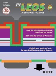
<strong>IEEE</strong>LASERS & ELECTRO-OPTICS SOCIETYNEWSLETTERFar-field pr<strong>of</strong>ile <strong>of</strong> VECSEL<strong>August</strong> 2005 Volume 19, Number 4FEATURES“The Center for Optoelectronic Devices, Interconnects and Packaging”N. Peyghambarian, R. Binder, M. Descour, M. Fallahi, D.F. Geraghty,H.M. Gibbs, S. Honkanen, G. Khitrova, A. Kost, R. Kostuk, F. Kueppers,P. Polynkin, M. Mansuripur, D.L. Mathine, S.B. Mendes, J.V. Moloney,R.A. Norwood, A. Schülzgen and T. Tkaczyk . . . . . . . . . . . . . . . . . . . . . . . . . . . .44DEPARTMENTS69News . . . . . . . . . . . . . . . . . . . . . . . . . . . . . . . . . . . . . . . . . . . . . . . . .13• Obituary: Richard B. Dyott• LEOS 2005 Meeting Announcement• LEOS Candidates for 2006-2008 Board <strong>of</strong> GovernorsCareers . . . . . . . . . . . . . . . . . . . . . . . . . . . . . . . . . . . . . . . . . . . . . . . .15• LEOS Pr<strong>of</strong>iles:* Indium Phosphide and Related Materials (IPRM 2005)Best Student Paper Award winner – Marcel W. Pruessner* 2000 <strong>IEEE</strong>/LEOS Graduate Student Fellowship recipient –Sarun Sumriddetchkajorn• Tools “Tips for Making Writing Easier: Part 6” and“How to Give Technical Presentations to Non-TechnicalAudiences: Part 3”Members . . . . . . . . . . . . . . . . . . . . . . . . . . . . . . . . . . . . . . . . . . . . . .19• Benefits <strong>of</strong> <strong>IEEE</strong> Senior Membership• New Senior Members• Reorganization <strong>of</strong> Membership CommitteeConferences . . . . . . . . . . . . . . . . . . . . . . . . . . . . . . . . . . . . . . . . . . . .23• ECOC 2005• Recognition at OFC 2005• Conference Calendar9Publications . . . . . . . . . . . . . . . . . . . . . . . . . . . . . . . . . . . . . . . . . . . .26• Call for Papers* <strong>IEEE</strong> Journal <strong>of</strong> Selected Topics in Quantum Electronics (JSTQE)* <strong>IEEE</strong>/OSA Journal <strong>of</strong> Display Technology (JDT)COLUMNSEditor’s Column………………2President’s Column………………….3<strong>August</strong> 2005 <strong>IEEE</strong> LEOS NEWSLETTER 1
President’sColumnH. SCOTT HINTONAwardsA few years ago I had the opportunity <strong>of</strong>presenting the <strong>IEEE</strong> <strong>Photonics</strong> Award toDr. Tingye Li, who I felt was one <strong>of</strong> thementors and teachers that helped me growup in the field. Prior to the <strong>of</strong>ficial awardsceremony there were many who came forwardto talk to Tingye and congratulatehim for receiving this award. I am surethat many <strong>of</strong> these people, like me hadalso been helped and influenced by Tingyeas their careers moved forward. I realizedat that time, that this award was not justfor Tingye, but it was also for all <strong>of</strong> us whohave been influenced and inspired by hisactions. It was a way for all <strong>of</strong> us, as wellas the entire technical community, tothank him for his contributions to thefield and to us as individuals. I came awayfrom that meeting with a better understanding<strong>of</strong> why LEOS has been soinvolved in providing awards for our pr<strong>of</strong>essionalcommunity.LEOS sponsors or jointly sponsorsseven major awards for leadership in ourfield <strong>of</strong> interest. They include theQuantum Electronics Award, the <strong>IEEE</strong><strong>Photonics</strong> Award, the <strong>IEEE</strong>/LEOSWilliam Streifer Scientific AchievementAward, the <strong>IEEE</strong>/LEOS EngineeringAchievement Award, the John TyndallAward, the Aron Kressel Award, theDistinguished Lecturer Awards, and theDistinguished Service Award. Thedescriptions for each <strong>of</strong> these major awardsare given below (See the “LEOS awards”page at www.i-leos.org).The Quantum Electronics Awardis given to honor an individual (orgroup <strong>of</strong> individuals) for outstandingtechnical contributions to quantumelectronics, either in fundamentals orapplications, or both. The Award maybe for a single contribution or for a distinguishedseries <strong>of</strong> contributions overa long period <strong>of</strong> time.The <strong>IEEE</strong> <strong>Photonics</strong> Award ispresented for outstanding achievementsin photonics. It may be presentedto an individual or a team <strong>of</strong> notmore than three.The <strong>IEEE</strong>/LEOS William StreiferScientific Achievement Award isgiven to recognize an exceptional singlescientific contribution which hashad a significant impact in the field <strong>of</strong>lasers and electro-optics in the past 10years. It may be given to an individualor to a group for a single contribution<strong>of</strong> significant work in the field.The <strong>IEEE</strong>/LEOS EngineeringAchievement Award is given to recognizean exceptional engineering contributionwhich has had a significantimpact on the development <strong>of</strong> laser orelectro-optic technology or the commercialapplication <strong>of</strong> technologywithin the past 10 years. It may begiven to an individual or to a group fora single contribution <strong>of</strong> significantwork in the field.The John Tyndall Award,endowed by Corning Inc., is presentedannually to a single individual who hasmade outstanding contributions in anyarea <strong>of</strong> optical-fiber technology,including optical fibers themselves,the optical components used in fibersystems, as well as transmission systemsand networks using fibers. Thecontributions which the award recognizesshould have met the test <strong>of</strong> timeand should have been <strong>of</strong> proven benefitto science, technology, or society.The contributions may be experimentalor theoretical. This award is jointlysponsored by the <strong>IEEE</strong> Lasers andElectro-Optics <strong>Society</strong> and the Optical<strong>Society</strong> <strong>of</strong> America.The Aron Kressel Award isgiven to recognize those individualswho have made important contributionsto opto-electronic device technology.The device technology cited isto have had a significant impact ontheir applications in major practicalsystems. The intent is to recognize keycontributors to the field for developments<strong>of</strong> critical components, whichlead to the development <strong>of</strong> systemsenabling major new services or capabilities.These achievements shouldhave been accomplished in a priortime frame sufficient to permit evaluation<strong>of</strong> their lasting impact. Thework cited could have appeared in theform <strong>of</strong> publications, patents, products,or simply general recognition bythe pr<strong>of</strong>essional community that theindividual cited is the agreed uponoriginator <strong>of</strong> the advance upon whichthe award decision is based.The Distinguished LecturerAwards program is designed to honorexcellent speakers who have madetechnical, industrial or entrepreneurialcontributions <strong>of</strong> high quality to thefield <strong>of</strong> lasers and electro-optics, and toenhance the technical programs <strong>of</strong>LEOS chapters. Consideration is givento having a balance <strong>of</strong> speakers whocan address a wide range <strong>of</strong> topics <strong>of</strong>current interest in the fields covered byLEOS. Eight Lecturers are selectedeach term (July 1-June 30) with someLecturers extending for a second term.Each Lecturer agrees to give a minimum<strong>of</strong> six lectures at LEOS chapters.The Distinguished ServiceAward was established to recognize anexceptional individual contribution <strong>of</strong>service which has had significant benefitto the membership <strong>of</strong> the <strong>IEEE</strong>Lasers and Electro-Optics <strong>Society</strong> as awhole. This level <strong>of</strong> service will <strong>of</strong>teninclude serving the <strong>Society</strong> in severalcapacities or in positions <strong>of</strong> significantresponsibility.As the society president I encourageyou to get involved in nominating thetechnical leaders that have inspired andmotivated you for these awards. If youhave any comments or suggestions, pleasecontact me at h.s.hinton@ieee.org.<strong>August</strong> 2005 <strong>IEEE</strong> LEOS NEWSLETTER 3
Government Research HighlightsThe Center for OptoelectronicDevices, Interconnects and PackagingN. Peyghambarian, R. Binder, M. Descour, M. Fallahi, D.F. Geraghty, H.M. Gibbs, S.Honkanen, G. Khitrova, A. Kost, R. Kostuk, F. Kueppers, P. Polynkin, M. Mansuripur,D.L. Mathine, S.B. Mendes, J.V. Moloney, R.A. Norwood, A. Schülzgen and T. TkaczykAbstractThe Center for Optoelectronic Devices, Interconnects andPackaging (COEDIP) is a multi-disciplinary program, bringingtogether research and educational programs in the areas <strong>of</strong> photonics,optoelectronics, chemistry, materials sciences, electricaland computer engineering and mathematics. COEDIP’s missionis to test innovative ideas, invent novel device concepts, packagestate-<strong>of</strong>-the-art devices and sub-systems, pursue emergingresearch opportunities, prepare students for dynamic careers inthe telecommunications and photonics industries, and supportthe creation and growth <strong>of</strong> collaborations between Universityand industry partners. The industrial funding <strong>of</strong> COEDIP isleveraged by the State <strong>of</strong> Arizona funded TRIF <strong>Photonics</strong>Initiative program to stimulate economic growth and enhanceeducation throughout the State.Center Mission and RationaleThe Center is dedicated to being a resource base to the scientificcommunity and a leading research and educational organizationworking toward a fundamental understanding <strong>of</strong> novel opticaldevices, device physics, fabrication <strong>of</strong> optoelectronic components,monolithic device integration and packaging.Signal Power @ 1535 nm (W)10864200 10 20 30Launched Pump Power @ 976 nm (W)Fig. 1 Left: Signal vs. launched pump power for a 7cm long laserusing the active fiber shown in the inset. Right: Microscope images<strong>of</strong> two types <strong>of</strong> microstructured optical fiber fabricated from phosphateglasses.UNIVERSITY OF ARIZONA, COLLEGE OF OPTICAL SCIENCES,1630 E. UNIVERSITY BLVD., TUCSON, AZ 85721Research Programs1. Compact High Power Fiber LasersThis program is aimed at the development <strong>of</strong> compact highpower microstructured, photonic crystal and other novel fiberlasers. Current high power fiber lasers are typically several metersto a hundred meters long. Short-length fiber lasers combine theadvantages <strong>of</strong> extremely compact sizes for device integration,reduced nonlinear effects for high-power continuous and pulsedoutput, and potential single frequency operation due to increasedlongitudinal mode spacing. We have achieved several Watts <strong>of</strong>output power from few cm-long fiber lasers. The researchincludes all major fiber laser design and fabrication issues. In particular,we optimize the active glass to enable extremely highEr 3+ and Yb 3+ doping levels; we design, fabricate and test specialfiber geometries and resonator configurations to maximizethe absorption <strong>of</strong> the pump light from multimode semiconductorlaser diodes, and we ultimately optimize the fiber laser efficiency[1]. An essential element <strong>of</strong> this success is the combination<strong>of</strong> experimental research with advanced 3D laser modeling.We have demonstrated more than 9W output power generatedusing a 7cm long fiber laser [2]. This corresponds to a recordpower <strong>of</strong> 1.3W/cm <strong>of</strong> active fiber in the 1550 nm region.Er 3+ /Yb 3+ co-doped phosphate glass served as the laser materialwith an emission wavelength <strong>of</strong> 1535 nm that is compatiblewith fiber based communication and sensing systems. Key tooptimizing the output power per length is a large area <strong>of</strong> activeglass that forms the fiber core. In step index fibers used for thepreviously described lasers the achievable core diameter is limitedto a maximum <strong>of</strong> about 20µm by the control over the differencebetween the refractive index <strong>of</strong> the core and cladding glasses.To overcome this limitation we started utilizing the novelconcept <strong>of</strong> active microstructure fibers where the inner claddingthat surrounds the doped core contains a periodic structure <strong>of</strong> airholes. Shown in Fig. 1 are the first microstructured fibers madefrom phosphate glass, the same glass that allowed extremelyhigh doping levels in the record breaking step index fiber lasers.In these examples the inner cladding with the air holes is madefrom undoped glass and one or seven unit cells, respectively, inthe center <strong>of</strong> the fiber are replaced by doped, active material. Forboth structures we demonstrated single-mode laser operation [3]with mode areas twice as large as in our best step-index fibers.Based on the development <strong>of</strong> the fabrication technology formicrostructured fibers we are currently building large core fiberlasers aimed at a 4W/cm power level. This will allow 10Wlasers from less than 3cm <strong>of</strong> fiber, which is short enough toselect just one frequency with narrow band fiber Bragg gratings.Such compact single frequency lasers have high potential aslight sources in remote coherent sensing. Another direction <strong>of</strong>4 <strong>IEEE</strong> LEOS NEWSLETTER <strong>August</strong> 2005
FBG in PM fiberFBGs in SM fiber11 cmsub-cavitypumppumpOuput power at 1535nm, mW2000150010005000-20dBm -40> 60dB-60-801520 1530 1540 155000 5 10 15 20Total pump power at 980nm, WFig. 2: Schematic <strong>of</strong> the fiber laser set up and its output characteristics.interest is the exploration <strong>of</strong> schemesthat are suitable for coherently combininga number <strong>of</strong> our fiber lasers into highpower output beams.2. Development <strong>of</strong> Watts-level Singlefrequencyand Short-pulse All-fiberLaser Oscillators at 1.5µm.We have developed a scalable and efficientmethod <strong>of</strong> optically pumping short,phosphate-glass active fibers fabricated atthe College <strong>of</strong> Optical Sciences [4]. Wenow use this pumping scheme to advancethe output power from all-fiber laseroscillators both continuous-wave, singlefrequency,and pulsed, into the Wattsrange. In particular, using the twistedmodecavity approach, we have demonstratedan output power <strong>of</strong> 1.9W from anall-fiber single-frequency laser oscillatorat 1.5µm. This output power is the highestamong single-frequency fiber laseroscillators reported to-date [5]. The lasersetup and power performance are summarizedin Fig. 2. In addition, we havedemonstrated 2.2W <strong>of</strong> output powerfrom a passively mode-locked fiber laserat a repetition rate <strong>of</strong> 100MHz. The minimumpulse width achieved so far is8psec. The laser schematic and the pulseautocorrelation trace are shown in Fig. 3.Work is under way to reduce the pulsewidth to below 1psec.3. High Power High BrightnessVECSELsHigh-power, high-brightness lasers aredesirable for a wide range <strong>of</strong> commercialand defense applications. Opticallypumped semiconductor vertical-externalcavitysurface-emitting lasers (VECSELs)are particularly attractive for their highpower and excellent beam quality [6]. Aschematic <strong>of</strong> an optically-pumped VEC-SEL is shown Fig. 4. This device is anextremely efficient converter ( > 50%optical-to-optical) <strong>of</strong> high power diodebarincoherent light into spectrally narrowand high brightness coherent emission.In these lasers, a semiconductormulti-quantum wells active region and adistributed Bragg reflector (DBR) stack,only a few microns thick, are mounted onthe heat spreader or heat sink, resultingin efficient heat dissipation which makesthe VECSEL a strong candidate forpower-scalable lasers. The external outputcoupler (mirror) controls transversemode operation. The active region consists<strong>of</strong> 14 InGaAs compressive strainedquantum wells combined with strainedcompensating GaAsP barriers. Thethickness and compositions <strong>of</strong> the layersare optimized such that each quantumwell is positioned at an antinode <strong>of</strong> thestanding wave <strong>of</strong> the laser field to provideresonant periodic gain (RPG) in the<strong>August</strong> 2005 <strong>IEEE</strong> LEOS NEWSLETTER 5
Side-pumped active fiberSESAM80%7dB coup ler21 cmpump600500Signal, a.u.40030020010013 psec0-15 -10 -5 0 5 10 15time, psecFig. 3: Schematic <strong>of</strong> the mode-locked fiber laser and its output.Fig. 4: Schematic <strong>of</strong> an optically-pumped VECSELVECSEL TEM 00 output (mW)Performance <strong>of</strong> DQW-4 (LR-coat.) at 15 o C (different spot)(r=10 cm, L=9 cm, defocussed 230µm pump spot)5000450040003500300025002000150010005000R=94%SE = 40 %2000 4000 6000 8000 10000 12000 14000 16000 18000Net pump power (mW)Fig. 5: Output power <strong>of</strong> the VECSEL4.8 WFig. 6: Far-field pr<strong>of</strong>ile <strong>of</strong> VECSELactive region. A DBR stack made <strong>of</strong> 25-pairs <strong>of</strong> AlGaAs/AlAs isgrown on the top <strong>of</strong> the active region. The fabrication <strong>of</strong> theVECSEL is critical to the laser performance. Figures 5 and 6show the TEM 00 output power and far-field <strong>of</strong> the VECSEL.Over 4W CW TEM 00 output and an M 2
6. Adiabatic Null-CouplersThis work is focused on a class <strong>of</strong> devices called adiabatic nullcouplers.These devices combine an asymmetric y-branch with aBragg grating. Our work focuses on the mode conversion providedby the Bragg grating, and how novel waveguide structurescan produce unique Bragg gratings which support new functionalities.We proposed and have recently demonstrated an antisymmetricgrating which provides more efficient mode conversionthan the traditional tilted Bragg grating while also preventingthe spurious reflections that tilted gratings produce. Fig.8 shows how the traditional tilted Bragg grating produces multiplereflection peaks, while the anti-symmetric grating producesonly the desired reflection. We have found that the experimentalresults are accurately predicted by our theoretical analysis. Weare developing null-coupler structures for optical packet headerrecognition, optical CDMA and optical encryption and are workingon experimental verification <strong>of</strong> these concepts.7. Edge Illuminated Polymer Holograms for CDMAApplicationsDuring the past few years there have been several importantdevelopments in polymers for holographic recording. One varietythat shows considerable promise is doped methyl methacrylate(MMA). In particular phenanthrene quinone (pq) dopedMMA can be form holograms in high optical quality substrates<strong>of</strong> up to 1cm thickness with high diffraction efficiency and lowshrinkage. We have been experimenting with this material tomake cascaded grating encoders and decoders for optical codedivision multiple access (CDMA) applications. An edge illuminatedhologram geometry as shown in Fig. 9 is used to extendthe effective thickness <strong>of</strong> the grating and to allow the formation<strong>of</strong> cascaded grating with different grating periods and separationsbetween gratings. This allows the realization <strong>of</strong> 2-dimensionalcodes for CDMA systems. We will be investigating a techniquefor implementing low matched encoders and decoders foruse in local area network and fiber-to-the-premise applications.(a)(b)Fig. 7: (a) Hybrid ion-exchange/sol-gel waveguide structure forbiosensing and (b) the measured signals at 632 nm and 532 nmwavelengths when ~1/2 monolayer <strong>of</strong> the cytochrome c protein isadsorbed to the hydrophilic waveguide glass surface.8. Nanophotonic Materials and DevicesThe objective here is to develop novel and low cost nano-opticaldevices for a wide range <strong>of</strong> photonic applications. We emphasizenew techniques for monolithic integration <strong>of</strong> active and passivesemiconductor devices. Our approach is to use ion implantationwith rapid thermal annealing to shift the band gap for selectedareas <strong>of</strong> a semiconductor chip and to create active regions forhigh optical gain and passive regions with low optical loss. Wealso use focused ion beam milling to fabricate nano-optical components.We have fabricated the first arrayed waveguide gratingsfor coarse wavelength division multiplexing using a unique “Sshaped”waveguide array. We have also demonstrated a worldrecord200nm band gap shift for GaAsSb quantum wells.9. CMOS BiochipCell-based biosensors are uniquely situated to obtain physiologicalresponses from live cells. These responses can give informationabout chemical toxicity, environmental pollutants andresponses to drugs. Our approach to a cell-based biosensor uses aCMOS substrate to integrate chemical, electrical, optical andcapacitive sensors into a single pixel. This multisensor integra-<strong>August</strong> 2005 <strong>IEEE</strong> LEOS NEWSLETTER 7
tion provides information about the cell’s health that is not possiblewith a single sensor.A cell-based biosensor requires control <strong>of</strong> the cell’s environmentto maintain viable cell cultures. We have used PDMSchambers to control the flow <strong>of</strong> the fluidic components <strong>of</strong> theculture, while preventing electrical shorting <strong>of</strong> the electricalleads. The temperature is maintained at 37.1°C via a thermoelectriccooler. This miniaturization provides the opportunityto include a variety <strong>of</strong> cell types on the same sensor. By includingkidney, heart, liver, etc. cells; a body-on-a-chip can bedeveloped to simultaneously obtain cellular responses from differentcell types.Our plan includes enhanced sensor development and integrationon the CMOS chip.0.80.60.40.210.80.601.55 1.5503 1.5506 1.5509 1.5512 1.5515 1.5518 1.5521 1.5524 1.5527 1.553Anti-symmetric Bragg gratingTGB(a)110. MicrosystemsA universal miniaturized platform for a variety <strong>of</strong> optical systemsis being developed. It is based on implementation <strong>of</strong> ultra-precisemicro-optics fabrication and assembly techniques. An example<strong>of</strong> an instrument based on this technology is a completemicroscope-on-a-chip for high resolution bio-imaging anddetection <strong>of</strong> precancerous cells (see Fig. 12). Specific technologiesused in the project include: (a) grayscale-lithography for fabrication<strong>of</strong> refractive lenslets in photopatternable hybrid glass; (b)development <strong>of</strong> Micro Optical Table (MOT) - an alignment freeapproach is pursued using silicon/metal springs and photolitographyfeatures providing submicron assembly precision; (c)CMOS technology for the development <strong>of</strong> a fast, small pixelimaging detector; (d) a scanning grating actuator made usingLIGA technology.All system components are integrated on the MOT platform,resulting in a miniaturized, packaged optical system. Along thecourse <strong>of</strong> the project several accomplishments were delivered.These include: (a) lenslet sag reached 100 µm, permitting fabrication<strong>of</strong> short-focal lenslet - surface roughness for the whole lenssurface is always below 20nm [16]; (b) the prototype system [17]has NA = 0.4 and magnification m = - 4 with demonstratedoptical system quality <strong>of</strong> the Strehl Ratio at 0.75 and higher; (c)demonstrated testing methodology for a 4M device and otherminiaturized optical systems [18]; (d) fast CMOS detectordesign. The pixel size is 4µm, frame rate is up to 500 images/sec.The pixel size allows 1µm spatial resolution while the frame ratepermits a real time structure illumination technique [19] - thetotal size <strong>of</strong> the CMOS is 2.6x1.5 mm 2 ; and (e) design <strong>of</strong> a scanninggrating actuator working in the frequency range <strong>of</strong> 50 -250Hz with an amplitude <strong>of</strong> ±100µm.0.40.201.55 1.5503 1.5506 1.5509 1.5512 1.5515 1.5518 1.5521 1.5524 1.5527 1.553(b)Fig. 8. Spectral reflectivity <strong>of</strong> (a) modeled anti-symmetric Bragggrating (solid), tilted Bragg grating (dashed) and (b) measuredanti-symmetric Bragg grating.Exposing BeamsFig. 9. The hologram is exposed in the conventional manner as shown on the left.After exposure the edges <strong>of</strong> the hologram are polished and illuminated from theedge. A series <strong>of</strong> gratings with different periods and separations are used toimplement an optical CDMA code for user identification.d1Ch 1 EncoderG1 G2 G nL11. Ultra-High-Speed Transmission SystemsSince photonic telecommunication networks continue to bemajor consumers <strong>of</strong> optoelectronic devices, a part <strong>of</strong> COEDIP’sresearch effort is dedicated to the improvement <strong>of</strong> efficiency andperformance <strong>of</strong> optical transmission on the system level. Thebenefit <strong>of</strong> this approach is tw<strong>of</strong>old: on one level the system layerpr<strong>of</strong>its from advanced components created within COEDIP,whereas at the same time the device level gets feedback withrespect to applications and requirements.Future networks will operate with higher line ratesthan today’s standard NX10 Gbit/s WDM technology.Several field trials with 40Gbit/s systems havebeen carried out by major network operators (MCI,Sprint, Verizon) in collaboration with leading systemmanufacturers (Ciena, Lucent Technolgies, Mintera).Recently installed transmission systems already <strong>of</strong>ferthe capability to accept 40Gbit/s line cards.Intensity modulated differential phase shift keying(IM DPSK) has become a promising candidate forsuch future long-haul WDM transmission systemsoperating at 40Gbit/s per wavelength channel.Numerous publications based on numerical andexperimental results showed its remarkable amenities,especially its robustness with respect to nonlinear distortions.For these demonstrations, different duty8 <strong>IEEE</strong> LEOS NEWSLETTER <strong>August</strong> 2005
cycles, ranging from < 1/4 to > 2/3, were applied. Nevertheless,a systematic study <strong>of</strong> the influence <strong>of</strong> the duty cycle itself on thetransmission performance <strong>of</strong> such IM DPSK systems had beenmissing and was conducted within COEDIP.The influence <strong>of</strong> the duty cycle in high-speed (40Gbit/s)long-haul (1,200km) transmission systems was investigated bymeans <strong>of</strong> numerical simulations. Two fiber types (standard single-modefiber SMF with conventional and alternating dispersioncompensation schemes and non-zero dispersion fiberNZDF), various signal power levels (-3 to +9dBm) and differentmodulation formats (conventional intensity modulation – nonreturn-to-zeroNRZ, return-to-zero RZ and carrier-suppressedreturn-to-zero CS-RZ – as well as CS-RZ DPSK) were taken intoaccount.As a result, shorter duty cycles tend to show superior performance(in terms <strong>of</strong> lower eye opening penalties) for all modulationformats, a fact, which is attributed to “more linear” transmissionfor shorter pulses.System optimization will be extended to ultra-high speeds <strong>of</strong>160Gbit/s in 2005. Additional influences such as dispersionfluctuation due to temperature changes will be taken intoaccount, and the effect <strong>of</strong> entering the so-called “quasi-linear”transmission regime will be investigated.infiltrated photonic crystals. The emphasis is on exploiting relativelywell-developed materials technologies in novel devicegeometries that enhance performance, as well as the demonstration<strong>of</strong> low-cost fabrication techniques that can lead to high-volumemanufacture. New materials are inserted within provendevice and fabrication platforms to provide for direct comparisonwith existing systems. An example <strong>of</strong> our approach is the hybridsol-gel/electro-optic polymer modulator shown in Fig. 13. Inthis device, sol-gel waveguides are used for coupling to opticalfiber, while an internal vertical adiabatic transition transfers thesingle-mode 1550nm radiation from the sol-gel waveguide intothe electro-optic polymer waveguide, where the phase <strong>of</strong> thelight is modulated by the Pockels electro-optic effect. The elec-12. Organic OptoelectronicsOur program in organic optoelectronics encompasses areas suchas electro-optic polymer modulators, organic light emittingdiodes, photorefractive polymers, sol-gel nanocomposites, andFig. 10. Broadband, arrayedwaveguide gratings on InPFig. 11. DAPI stained COS-7cell attached directly to a CMOSchip. The electrode pattern isvisible in the image.
tro-optic polymer layer is poled by either corona or contact polingtechniques. The figure further shows the optical modulationachieved, as measured through crossed polarizersThus far, phase modulators have been demonstrated with 7-8dB <strong>of</strong> insertion loss and half-wave voltages <strong>of</strong> 13V, for a 2.4cmdevice using an electro-optic polymer with r 33 = 25 pm/V in thedevice. We have recently developed techniques that will allow usto achieve 2 to 3 times higher r 33 within the device, leading toa subsequent reduction <strong>of</strong> Vπ by the same factor. Adoption <strong>of</strong>higher activity electro-optic polymers and Mach-Zehnderdesigns will result in an additional factor <strong>of</strong> 3 to 4, leading to Vπin the range <strong>of</strong> 1V. In parallel with these activities, we have nowdeveloped lower-loss organically modified sol-gel systems thattake advantage <strong>of</strong> partial fluorination to reduce infrared absorptionfrom vibrational overtones. This is expected to help us t<strong>of</strong>urther reduce the insertion loss below the 5 dB level.Fig. 12. Scheme <strong>of</strong> the complete microscope-on-a-chip for high resolutionand reflected light in the tissue.Fig. 13 Hybrid sol-gel/EO polymer modulator showing modulationachieved.log ( εT/ εin)0-2-41 4 7T d/ T wFig. 14: Logarithmic plot <strong>of</strong> the transmitted pulse energy ε T inunits <strong>of</strong> the input pulse energy ε in vs the delay time T d in units <strong>of</strong>the pulse duration T W , for 2000 quantum wells (solid line). For200 quantum wells (dotted line), only the energy <strong>of</strong> the delayedportion <strong>of</strong> the pulse is counted. For comparison, we plot a linearfunction with slope 2γ as the dash-dotted line, which shows that thedecay <strong>of</strong> the transmitted pulse is slower than the hypothetical rategiven by the non-radiative decay and dephasing <strong>of</strong> the quantumwell polarization.13. Stopping, Storing and Releasing Light in Quantum WellBragg StructuresA major goal <strong>of</strong> our theoretical research is to develop a semiconductordevice that allows for the stopping, storing and releasing<strong>of</strong> light pulses and could be used, for example, as optical delayline. In collaboration with the University <strong>of</strong> Iowa, we are currentlystudying light propagation and manipulation in onedimensionalresonant photonic bandgap structures. Specifically,we are studying trapping <strong>of</strong> picosecond optical pulses in quantum-wellBragg structures, which are multiple quantum wellsspaced at approximately half the wavelength that corresponds tothe lowest exciton resonance in the individual quantum wells.The photonic bandstructure <strong>of</strong> the system exhibits a small transmissionwindow adjacent to the Bragg frequency if the excitonresonance is slightly detuned. Trapping and delaying <strong>of</strong> a lightpulse can be achieved if this transmission window is closed whilethe pulse is inside the structure. Reopening <strong>of</strong> the transmissionwindow releases the light pulse.From our numerical simulations <strong>of</strong> light delay in theses structures,we found that large (almost ideal) systems with 2000quantum wells allow for efficient trapping and storing <strong>of</strong>picosecond pulses. For example, Fig. 14 shows that a 4-bit delay<strong>of</strong> a pulse with duration T W = 6ps is accompanied by an energyloss <strong>of</strong> only about 10dB. We found that, for the parameters usedin this simulation, the loss is not dominated by the rate γ whichaccounts for dephasing and non-radiative decay <strong>of</strong> the excitonicpolarization in the individual quantum wells (γ = 0.1meV in thecalculation). Short structures with, for example, 200 quantumwells, have inferior delay-line characteristics, as shown for a 3pspulse in Fig. 14.In 2005, we plan to extend our analysis <strong>of</strong> optical delay inquantum well Bragg structures, including for example, furtherwork on anti-reflection coating <strong>of</strong> Bragg structures and pulsedeformation compensation. We also plan to study non-linearoptical effects as well as the issue <strong>of</strong> polarization switching inthese structures.14. True Strong CouplingA quantum well planar microcavity can exhibit normal modecoupling or vacuum Rabi splitting (VRS) if the excitonlinewidth is narrow enough and the cavity Q high enough. This10 <strong>IEEE</strong> LEOS NEWSLETTER <strong>August</strong> 2005
system is analogous to many-atom VRS,and operates in the nonperturbativeregime which is distinctly different fromthe regime <strong>of</strong> strong coupling (nevertheless,many semiconductor physicists callit “strong coupling”). Consequently, itsproperties can be understood semi classically,i.e. the electromagnetic field can betreated classically [20]. Quantum effects,e.g. matter-photon entanglement, areneeded for quantum information processing,and they are most pronounced in thestrong coupling regime, where the VRSis due to a single atom or single quantumdot (SQD). Several years ago, we reportedprogress toward strong coupling using aquantum well in a 3D oxide-aperturemicropillar and predicted strong couplingusing a SQD [21]. True strong couplingoccurs when the coupling gbetween the dipole moment µ <strong>of</strong> a SQDtransition and the vacuum field fluctuationsin the cavity mode exceeds both thedephasing rate γ <strong>of</strong> the SQD transitionand the loss rate κ <strong>of</strong> energy out <strong>of</strong> thecavity. Spectrally this means that thesplitting 2g must be larger than the coupledsystem linewidth (κ + γ)/2 for zerodetuning (when the eigenenergies <strong>of</strong> theSQD transition and cavity mode aredegenerate); otherwise, the emission isnot double-peaked, and the splitting isnot resolved. Whereas QD transitionlinewidths in the range 10-100 µeV havebeen reported, typically Q values havebeen only ~1000, resulting in κ = ν/Qvalues <strong>of</strong> order 1meV. Therefore, the goalhas been to maximize γ/ κ∝Q/√V in therace for strong coupling. Recently,Noda’s group achieved a Q <strong>of</strong> 45,000 fora new photonic crystal cavity design inSi; applying that design to the fabrication<strong>of</strong> a photonic crystal slab nanocavity inGaAs, Tomo Yoshie and Axel Scherer atCaltech obtained Q = 20,000 in some <strong>of</strong>the nanocavities with a computed V ≅0.04µm 3 [22]. Last year we observed truestrong coupling in one <strong>of</strong> their nanocavitiescontaining InAs dots grown by OlegShchekin and Dennis Deppe at theUniversity <strong>of</strong> Texas in Austin. Doublepeakedemission was resolved at zerodetuning, and the characteristic anticrossingrepulsion <strong>of</strong> the coupled systemeigenenergies was mapped out by scanningthe uncoupled energies through oneanother; see Fig. 15, where 2g ≅ 41GHz,κ≅42GHz, and γ≅21.5GHz [22]. Thissolid-state quantum system entangles thequantum dot transition qubit with thecavity photon qubit; someday it may beused for quantum state transfer or for aquantum phase flip gate. In order to controlthis strongly coupled system we needto learn how to access it more directly,perhaps by coupling it to a photonic crystalwaveguide. Further, we hope to climbthe Jaynes-Cummings ladder, with eachhigher rung having one more photon inthe nanocavity. The vacuum Rabi splittingreported above was seen in photoluminescencefrom rung one to rung zero.Evidence for the second rung with √2larger splitting would show that theSQD is small enough for the system to betruly quantum and therefore suitable forentanglement applications.AcknowledgementsThese works are supported by Corning,IFOS, Inc., Nitto Denko, NorthropGrumman, NP <strong>Photonics</strong>, Nippon SheetGlass, Samsung Electronics Co., Ltd.,Sony, Terapixel, DARPA, ONR, ARO,NSF, AFOSR and the Technology andResearch Initiative Funding (TRIF) fromthe State <strong>of</strong> Arizona.References1. L. Li, M. M. Morrell, T. Qiu, V. L.Temyanko, A. Schülzgen, A. Mafi, D.Kouznetsov, J. V. Moloney, T. Luo, S.Jiang, and N. Peyghambarian, “ShortCavityDotIncreasingTemperature1182.25 1182.50 1182.75 1183.00Wavelength (nm)Fig. 15 Dot-nanocavity anti-crossing. Thetemperature is increased in 1°K steps startingwith 13°K at the top and reaching29°K at the bottom. The two coupled-systempeaks (black lines are eye guide) areplotted as a function <strong>of</strong> temperature andcompared with the scan rates <strong>of</strong> an uncoupledQD (red curve) and the empty cavity(blue). The PL peaks anti-cross instead <strong>of</strong>following the crossing <strong>of</strong> the dot and cavityresonances.<strong>August</strong> 2005 <strong>IEEE</strong> LEOS NEWSLETTER 11
Cladding-Pumped Er/Yb Phosphate Fiber Laser with 1.5 WOutput Power,” Appl. Phys. Lett. 85, 2721 (2004).2. T. Qiu, L. Li, A. Schülzgen, V. L. Temyanko, T. Luo, S.Jiang, A. Mafi, J. V. Moloney, and N. Peyghambarian,“Generation <strong>of</strong> 9.3-W Multimode and 4-W SinglemodeOutput from 7-cm Short Fiber Lasers,” <strong>IEEE</strong> Phot. Tech.Lett. 16, 2592 (2004).3. L. Li, A. Schülzgen, V. L. Temyanko, T. Qiu, M. M.Morrell, Q. Wang, A. Mafi, J. V. Moloney, and N.Peyghambarian, “Short-length Microstructured PhosphateGlass Fiber Lasers with Large Mode Areas,” Opt. Lett. 30,1141 (2005).4. P. Polynkin, V. Temyanko, M. Mansuripur and N.Peyghambarian, “Efficient and scalable side pumpingscheme for short, high power optical fiber lasers andamplifiers,” <strong>IEEE</strong> Phot. Tech.Lett. 16, 1 (2004).5. P. Polynkin, A. Polynkin, M. Mansuripur and N.Peyghambarian, “Single-Frequency, Linearly Polarized FiberLaser with 1.9W Output Power at 1.5um Using Twisted-Mode Technique,” in Proc. CLEO 2005, Baltimore, MD,May 22-27, 2005, postdeadline paper CPDB11.6. L. Fan, M. Fallahi , J. Hader, A. R. Zakharian, M.Kolesik, J. V. Moloney, T. Qiu, A. Schülzgen, N.Peyghambarian, W. Stolz, S. W. Koch and J. T. Murray,“Over 3-W high-efficiency vertical-external-cavity surface-emittinglasers and application as an efficient fiberlaser pump source,” Appl. Phys. Lett. 86, 211116 (2005).7. J. Hader, J.V. Moloney, S.W. Koch and W.W. Chow,“Microscopic modeling <strong>of</strong> gain and luminescence insemiconductors,” <strong>IEEE</strong> J. Sel. Topics in Quant.Electron. 9, 688 (2003).8. A.R. Zakharian, J. Hader, J.V. Moloney, S.W. Koch, P.Brick and S. Lutgen ”Experimental and TheoreticalAnalysis <strong>of</strong> Optically Pumped Semiconductor DiscLasers,” Appl. Phys. Lett. 83, 1313 (2003).9. J. Carriere, J. Franz, B. Youmans, S. Honkanen, and R.Kostuk, “Measurement <strong>of</strong> waveguide birefringence usinga ring resonator,” <strong>IEEE</strong> Phot. Tech. Lett. 16, 1134(2004).10. J. Castro, D. Geraghty, B. West, and S. Honkanen,“Fabrication and comprehensive modeling <strong>of</strong> ionexchangedBragg optical add-drop multiplexers,”Appl. Opt. 43, 6166 (2004).11. S. Yliniemi, B. West, and S. Honkanen, “Ion-exchangedglass waveguides with low birefringence for a broad range<strong>of</strong> waveguide widths,” Appl. Opt., in press.12. P. Madasamy, S. Honkanen, D. Geraghty, and N.Peyghambarian, “Single-mode tapered waveguide laser inEr-doped glass with multimode-diode pumping,” App.Phys. Lett. 82, 1332 (2003).13. B. West and S. Honkanen, “MMI devices with weakguiding designed in three dimensions using a geneticalgorithm,” Opt. Express 12, 2716 (2004).14. B. West, P. Madasamy, N. Peyghambarian, and S.Honkanen, “Modeling <strong>of</strong> ion-exchanged glass waveguidestructures,” J. Non-Cryst. Solids 347, 18 (2004).15. J. Auxier, M. Morrell, B. West, S. Honkanen, A.Schülzgen, N. Peyghambarian, S. Sen, and N. Borelli,“Ion-exchanged waveguides in glass doped with PbSquantum dots,” Appl. Phys. Lett. 85, 6098 (2004).16. J.D.Rogers, A. Kärkkäinen, T. Tkaczyk, J.T. Rantala andM. Descour, “Realization <strong>of</strong> refractive microopticsthrough grayscale lithographic patterning <strong>of</strong> photosensitivehybrid glass,” Opt. Exp. 12, 1294 (2004).17. M.R. Descour, A. Karkkainen, J.D. Rogers, L. Chen, R.S.Weinstein, J.T. Rantala, B. Kilic, E. Madenci, R.R.Richards-Kortum, E.V. Anslyn, R.D. Dupuis, R.J. Schul,C.G. Willison and C.P. Tigges, “Toward the development<strong>of</strong> miniaturized imaging systems for detection <strong>of</strong> pre-cancer,”<strong>IEEE</strong> JQE 38, 122 (2002).18. J. Lee, J.D. Rogers and M. Descour, “Imaging qualityassessment <strong>of</strong> multi-modal miniature microscope,” Opt.Exp. 11, 1436 (2003).19. T. Tkaczyk, E. Dereniak, S. Gaalema, W. Bahn, S. Sun, T.Erickson, J.D. Rogers, T. Christenson, R. Richards-Kortum and M.R. Descour, “High speed CMOS for structuredillumination technique,” SPIE Proc. 5726 (2005).20. G. Khitrova, H. M. Gibbs, F. Jahnke, M. Kira, and S. W.Koch, “Nonlinear optics <strong>of</strong> normal-mode coupling semiconductormicrocavities,” Rev. Mod Phys. 71, 1591 (1999).21. C. Ell, H. M. Gibbs, G. Khitrova, E. S. Lee, S. Park, D.G. Deppe, and D. L. Huffaker, “Toward quantumentanglement in a quantum-dot nanocavity,” LEOSNewsletter 13(4), 8 (1999).22. T. Yoshie, A. Scherer, J. Hendrickson, G. Khitrova, H. M.Gibbs, G. Rupper, C. Ell, O. B. Shchekin, and D. G. Deppe,“Vacuum Rabi splitting with a single quantum dot in aphotonic crystal nanocavity,” Nature 432, 200 (2004).12 <strong>IEEE</strong> LEOS NEWSLETTER <strong>August</strong> 2005
NewsRichard B Dyott F<strong>IEEE</strong>Born Tientsin, China19th June 1924Died Chicago, USA29th March 2005Dick Dyott was born the instinctiveengineer. As a youngster at HarrowSchool he occupied the erstwhile study <strong>of</strong>Winston Churchill. On visiting his formerquarters with the Headmaster <strong>of</strong> theday, the great man expressed surprise atthe clutter <strong>of</strong> wires, cats’ whiskers andcrystals which adorned the room. Dick’sreply – a very assertive “But Sir, I wantto be a radio engineer”.Dick went on to spend more thanhalf a century as exactly that. His earlydays were in radar, the land <strong>of</strong> klystronsand ripple beam amplifiers in the immediatepost Second World War period atGEC’s Hirst laboratories in Wembley,London, now a supermarket, to Dicksymbolising graphically the demise <strong>of</strong>UK engineering. By the late 1960’s hehad developed his enduring interest infibre optics, simulating the double crucibleprocess using – to his management’shorror – cups <strong>of</strong> molten sugar“they were like Lady Bracknell” heprotested “Sugar!!!….”. Dick’s stronglyintuitive microwave background didhowever always make him cautious <strong>of</strong>circular fibre’s natural symmetry and thepolarisation problems that thisinevitably caused. Neither did he eversubscribe to the appeal <strong>of</strong> the low indexdifference. “You can’t bend it”.His early fibre work was at the PostOffice (now BT) laboratories in NorthLondon where not only was the trendtowards the circular but at the time multimodewas also the ethos, anotheranathema to Dick. BT moved toMartlesham Heath in fields and flatlandsand Dick, unwilling to leave his belovedLondon, where he could sing Berlioz inSt Paul’s and find outlets for his numerousother interests (which included ESPand telepathy!!) moved to ImperialCollege supported by AndrewCorporation based in Chicago. There hehad the opportunity to move from circularsymmetry into early crystal core fibresand in time to the tightly bound highindex difference elliptical core whichcontinued to dominate his activities fortwenty or so years. He moved toChicago, set up the e-core facility andwas the driving force behind fibre gyroprogrammes at Andrew (and laterKVH). In Chicago he could also sing,which he did with the SouthwestSymphony for many years, becoming itsPresident just before he died.Dick had many friends throughoutthe world. There were those to whom hepresented samples <strong>of</strong> elliptical core fibreto try out crazy ideas and odd experiments.There are many who delighted inhis company, regaled by endless stories <strong>of</strong>the Trans Siberian Express, or amorousmischief on the Metropolitan Line on theLondon Underground. He tookimmense delight in his work. He revelledin the positive and applied doggedingenuity to the setbacks with which weare all familiar. He believed in trying thelong shot experiment “on a Friday afternoon”.Many <strong>of</strong> these were successful. Hedelighted too in frustrating the “topbrass” for whom he always retained amischievous (<strong>of</strong>ten justified) disrespect.He was more the Rueb Goldberg, theHeath Robinson, than the complex programme.He was also immenselyrespected, recipient <strong>of</strong> SPIE’s TechnologyAchievement Award, recognised as an<strong>IEEE</strong> Outstanding Engineer and awardeda DSc from London University.Dick will be remembered with affectionand admiration, whether a scientistor chorister. We enjoyed his companytogether with Jan, his close companionin the US, for over twenty years. Heretained close contact with family inLondon and was immensely proud <strong>of</strong> histhree daughters and his much lovedgrandson. He was the inventor, scientist,innovator, never politician, never seeker<strong>of</strong> glory. He was that very rare being, thegreen-fingered engineer.Brian Culshaw:University <strong>of</strong> Strathclyde, UKAlan Rogers:Polarimetrix Limited, UKReg Russell: RetiredAlan Reddish: Retired<strong>August</strong> 2005 <strong>IEEE</strong> LEOS NEWSLETTER 13
News (cont’d)LEOS 2005 Meeting AnnouncementLEOS 2005, to be held the 23rd –27th <strong>of</strong> October in Sydney, Australia, isthe 18th Annual Meeting <strong>of</strong> the <strong>IEEE</strong>Lasers and Electro-Optics <strong>Society</strong>(LEOS). This conference has establisheditself as an important event for the latestdevelopments in lasers and electrooptictechnologies. With a strong core<strong>of</strong> invited talks given by preeminentspeakers from around the globe, LEOS2005 will provide an ideal platform tolearn about new fields and understandnew technological trends.One <strong>of</strong> the LEOS charters is to promotecareer awareness among studentsand young researchers in photonics andrelated fields. New for this year the2005 LEOS Annual Meeting will host a“Careers in Research” Forum whichwill take place on Sunday October 23.Attendees will have the opportunityto:• Listen to presentations from academia,industry, and entrepreneurshighlighting milestones for achievingsuccess.• Listen to LEOS student awardwinners.• Interact with the highlightedspeakers.• Present poster papers <strong>of</strong> theirresearch.The “Careers in Research”Forum is soliciting submissionsfrom students and research groupsfor poster presentations. In additionto focusing on the results specificto the individual, the posterscould also highlight the broaderresearch area <strong>of</strong> the research group.To be considered the 35 wordabstracts should be submitted as apart <strong>of</strong> regular papers submissionto LEOS Annual Meeting. Theguidelines for posters will be publishedon LEOS web site(www.ieee.org/organizations/society/leos/LEOSCONF/LEOS2005).LEOS Candidatesfor 2006-2008Board <strong>of</strong> GovernorsBallots for the election <strong>of</strong> candidates to the Board <strong>of</strong>Governors will be mailed soon to all voting members.This year’s candidates are:Carmen MenoniColorado StateUniversityMarkus AmannWalter SchotkyInstituteMichael HaydukAir Force ResearchLabHideo KuwaharaFujitsu Laboratories,Ltd.David PlantMcGillUniversityS.J. Ben YooUniversity <strong>of</strong>CaliforniaAlwyn SeedsUniversity CollegeLondonKent ChoquetteUniversity <strong>of</strong>Illinois14 <strong>IEEE</strong> LEOS NEWSLETTER <strong>August</strong> 2005
Career SectionIndium Phosphide & Related Materials(IPRM 2005) Best Student Paper Award RecipientMarcel W. PruessnerMarcel W. Pruessner received the B.S. andM.S. degrees in electrical engineeringfrom the University <strong>of</strong> Maryland, CollegePark in 1998 and 2002, respectively. Heis currently working towards the PhDdegree, also in electrical engineering.In 1999 he worked at the U.S. Patentand Trademark Office in Arlington,Virginia as a Patent Examiner. From 1999-2000 he was aFaculty Research Assistant at the Institute for Research inElectronics and Applied Physics at the University <strong>of</strong>Maryland. His research focused on electron beam positionsensing and control electronics for an accelerator ring project.Since 2000 he has been a graduate research assistant inthe MEMS Sensors and Actuators Lab (MSAL) at theUniversity <strong>of</strong> Maryland, College Park, under the guidance<strong>of</strong> Pr<strong>of</strong>. Reza Ghodssi.His graduate research focuses on indium phosphideoptical waveguide microelectromechanical systems(MEMS). This work is supported by the National ScienceFoundation (NSF) and the Laboratory for Physical Sciences(LPS). The research combines waveguide integrated opticswith micromechanical components and semiconductormicromachining. Mr. Pruessner has developed severaltypes <strong>of</strong> low-power electrostatically actuated waveguideall-optical switches. Currently, his research focuses onmicromechanical resonators integrated with cantileverwaveguides for sensing applications.Mr. Pruessner is a student member <strong>of</strong> the <strong>IEEE</strong>/LEOS societyas well as Phi Beta Kappa (elected 1998), and he is therecipient <strong>of</strong> a 2003-2004 Achievement Rewards for CollegeScientists (ARCS) fellowship (Washington, D.C. Chapter).It is an honor to receive the Indium Phosphide andRelated Materials (IPRM) Best Student Paper Award. Onbehalf <strong>of</strong> my co-authors (Madhumita Datta, KuldeepAmarnath, S. Kanakaraju, and Reza Ghodssi), I thank theIPRM technical committee for giving our paper thisrecognition as it encourages our continued efforts in thisexciting field combining photonics and MEMS.
Career Section (cont’d)2000 <strong>IEEE</strong>/LEOS Graduate StudentFellowship RecipientSarun SumriddetchkajornSarun Sumriddetchkajornreceived his Ph.D. inOptical Science and Engineeringfrom the University<strong>of</strong> Central Floridain 2000 based on hiswork in fiber-optic beamcontrol systems underthe direction <strong>of</strong> Pr<strong>of</strong>.Nabeel A. Riza. Duringhis stay in the US as a graduate student, he received severalawards including the 1999 Optical <strong>Society</strong> <strong>of</strong> America(OSA)’s New Focus Student Award, the 1999 Motorola’sVirtual Display Outstanding Proposal Award, the 2000International <strong>Society</strong> for Photo-Optical InstrumentationEngineers (SPIE)’s “D. J. Lovell” Award, and the <strong>IEEE</strong>-LEOSGraduate Fellowship Award.After completion <strong>of</strong> his Ph.D., he became a photonics engineerat Nuonics, Inc. in Florida responsible for the development<strong>of</strong> fiber-optic processors using microelectromechanical system,liquid crystal, and acousto-optic technologies. In 2001, hereturned to his home country, Thailand, working as a researcherin the Electro-Optics Section at the National Electronics andComputer Technology Center. His current research is in thephotonic area where he applies photonics to solve problems forindustrial, medical, and environmental applications.Based on his work in optical touch switches and fiber-opticcomponents for telecommunications, he received the 2003Young Technologist Award and the 2004 Young ScientistAward from the Foundation for the Promotion <strong>of</strong> Science andTechnology under the Patronage <strong>of</strong> His Majesty the King. Inaddition, he initiated the formation <strong>of</strong> the OSA, <strong>IEEE</strong>-LEOS,and SPIE Thailand Chapters in order to dissiminate optics andphotonics to Thai society. Recently, he has also been awardedthe 2005 ICO-ICTP prize from the International Commissionfor Optics (ICO) and the Abdus Salam International Centre forTheoretical Physics (ICTP) for his achievements in applyingoptics and photonics to biomedical devices and telecommunicationsas well as for his interest in diffusing optics and photonicsin Thai society.“The 2000 <strong>IEEE</strong>-LEOS Graduate Fellowship given to me atthe year I completed my Ph.D. work has greatly contributed tomy research career. At that time, I had an opportunity to attendthe LEOS Annual Meeting in Puerto-Rico where I learned a lot<strong>of</strong> things in technical sessions as well as through discussionswith several well-known scientists. I am really thankful to allcommittee members and my advisor for laying some good seedsto me both directly and indirectly. It is indeed an excellent wayto motivate good people and bring them to the society. Thankyou very much.The other 2000 LEOS Graduate Student Fellowship Awardrecipients were featured in the April 2005 issue <strong>of</strong> the LEOSNewsletter.TOOLSTips for Making Writing EasierPeter Reimold and Cheryl ReimoldPart 6: Toning YourFirst DraftUp – Or DownPerhaps the greatest help for speedystyle editing is knowing what kind <strong>of</strong>“drafter” you are. Some people whowrite their drafts quickly, letting theirideas pour out without thinking aboutthe form they take (as we are advocating),produce chatty, somewhat sloppyprose that needs toning up; others producelong-winded paragraphs full <strong>of</strong>stuffy language and complex constructions.If you know where your troublestend to lie, you’ll find it easier to applyquick editing touches.In this column we give you sometips for both streamlining a chattydraft and simplifying convolutedprose. To explore your own style needsin more depth, you can visit our Website, http://www.allaboutcommunication.com,and take the style test postedthere. Review the eight style rulesin the test. Are there any that you<strong>of</strong>ten violate in your first drafts? Thenlearn how to fix those weak spotsquickly.Toning UpGetting Rid <strong>of</strong> AwkwardTransition ClutterIn a previous column we discussed oneorganizational remedy for chatty prose:Add headings and turn text into listswhere appropriate. This immediatelygives your piece a crisper, more businesslikeflavor. For instance, supposeyou find many clumsy transitionphrases such as “With regard to X…”or “As far as Y is concerned….” Thensimply create subheadings for X, Y,etc., begin each section with the main16 <strong>IEEE</strong> LEOS NEWSLETTER <strong>August</strong> 2005
Career Section (cont’d)TOOLSidea, and present details as a bullet list.After that quick touch there may belittle else left for you to change!Smoothing Out a Choppy StyleDo your paragraphs typically containmany short sentences in a row, or isthere some reasonable balance betweenlong and short? If you have nothingbut short sentences, the piece willappear choppy. The remedy is simple:Group some ideas that belong togetherand join them with informative connectorssuch as because, if, when, but,or although. For instance, take thisparagraph <strong>of</strong> four short sentences:We evaluated new and used XYZmachines. We concluded from ourtest that it was sufficient to install aused XYZ machine. The installationwould require an initial capitalinvestment <strong>of</strong> less than USD 30 000.The annual savings from this investmentwere calculated as USD 45 000.This can be made clearer and lessmonotonous by grouping the materialinto two sentences with helpfultransitions:From our evaluation <strong>of</strong> new andused XYZ machines, we concludedthat it was sufficient to install a usedmachine. Such an installation wouldrequire an initial capital investment <strong>of</strong>less than USD 30 000 but yield annualsavings <strong>of</strong> USD 45 000.Sharpening Your Word Choice“Write as you speak” is great advice forproducing a natural style, but it canbackfire if you tend to speak imprecisely.If you know that is your habit,check that your words express yourmessage accurately.Take the ugly verb impact, as inimpact our bottom line. Is the impactgood or bad? The reader has no idea.Words such as improve, worsen, raise,or lower give that helpful information.One frequent trouble spot is theword and used as a sentence connector.Often a more specific transition wordsuch as nevertheless or therefore would bemore helpful to the reader. Forinstance, consider the and in the followingsentence: As you might guess,no single test has all the answers andwe like to look at a range <strong>of</strong> tests tounderstand a particular printing systemissue.Replacing and with instead wouldbe a good way to make the sentencemore informative and pr<strong>of</strong>essional: Asyou might guess, no single test has allthe answers; instead, we like to look ata range <strong>of</strong> tests to understand a particularprinting system issue.Toning DownNow let’s confront the opposite problem:convoluted first drafts with overlyfancy words and complex, long sentencesthat are hard to read. We <strong>of</strong>ferthree simple ways to fix such commonproblems.Simple WordsOne easy way to make your pieceshorter and more energetic is to replacelong, Latin-based words such as cognizantor possess with shorter, simplerones such as aware or have. Here aresome other stuffy expressions and theirsimpler versions:a sufficient number <strong>of</strong> = enoughafford an opportunity to = allowin reference to = aboutprovide a means whereby = enablepursuant to these guidelines = underthese guidelinesremunerate/remuneration = payrender assistance to = help, assistSome <strong>of</strong> your fancy words may alsoinvite misunderstanding. For instance,exceptionable means objectionable, and isnot to be confused with exceptional (=out <strong>of</strong> the ordinary). Since readers maynot know the difference, it’s best tostay clear <strong>of</strong> such dangerous wordsaltogether.Simple Sentence ConstructionsTake a look at your sentences. Domany have more than two clauses orspan more than two lines? This happensmost frequently with technicalwriting, as in this example:Visual and microscopic inspections<strong>of</strong> the samples, which were coated withthree layers <strong>of</strong> formulation 1 and driedin an IR oven at 300ºF after each coating,showed that samples 1-6 had verygood surface quality, and they alsopassed the tape adhesion test, whilegloss was somewhat lower than in thecontrol sample.This sentence boasts four clausesand several thoughts. To simplify,break up some <strong>of</strong> the sentences, at leastthose with more than one thought. Ifyou follow the rule <strong>of</strong> “one thought toa sentence,” you will change that overloadedmonster into three readablesentences:Visual and microscopic inspections<strong>of</strong> the samples showed that samples 1-6 had very good surface quality butsomewhat lower gloss than the controlsample. They also passed the tapeadhesion test. These samples had beengiven three coats <strong>of</strong> formulation 1 andwere dried in an IR oven at 300ºF aftereach coating.Active VerbsOne weakness in almost all businesswriting is overuse <strong>of</strong> the passive voice,as in:The study, which had beenrequested by management a yearago, was completed by the team inlate May.Simply state who does what (activevoice) rather than what was done (passive),unless knowing the agent is <strong>of</strong> nointerest to the reader. It cuts out words<strong>August</strong> 2005 <strong>IEEE</strong> LEOS NEWSLETTER 17
Career Section (cont’d)TOOLSand avoids many grammar errorsintroduced by the passive voice. Theexample then becomes:The team completed the study,which management had requested ayear ago, in late May.Similarly, the 14-word passivesentence:It is recommended that this matterbe brought up at the next team meeting.Becomes the clearer 11- wordactive sentence:We recommend taking up thismatter at the next team meeting.Whether your drafts need toningup or down, it can be a pleasureto watch these few simple techniquesallow the clarity <strong>of</strong> yourthought to shine through! AsRobert Frost put it, “All the fun’sin how you say a thing.”How to Give Technical Presentationsto Non-Technical AudiencesPeter Reimold and Cheryl ReimoldPart 3: Magic QuestionsYou have been told to give a presentationon your project to peoplefrom different areas <strong>of</strong> the company.What is the first question you askyourself? If you are like most people,it is “What on earth am I goingto tell them about it?”That question is the reason mostpresentations go <strong>of</strong>f the rails. Why?Well, it sends the presenter straight tothe subject <strong>of</strong> the talk to look for themost interesting or important details<strong>of</strong> it. And here is the sad part: The featuresthat most fascinate the technicalexpert (you) are almost guaranteed tosend the non-technical listeners (youraudience) into loud, painful yawns.Say you’re presenting theresults <strong>of</strong> work done to resolve customercomplaints on your company’stop-selling product. Youranalysis <strong>of</strong> specks contaminating arecent sample showed a few <strong>of</strong>them to be bits <strong>of</strong> ABC instead <strong>of</strong>the anticipated EFG. That is mostsurprising to you as it suggests thepresence <strong>of</strong> certain unexpectedminerals in the water used to preparethe product. The discovery isimportant to you in another way asit was made on the new spectroanalyticalmachine you had persuadedthe company to buy. You arepretty sure the old machines wouldnot have detected the tiny amounts<strong>of</strong> ABC.How much do you think thesales representatives in your audiencewill care about those momentousfindings? Or the people fromaccounting? Gripping as they maybe to you, the facts by themselvesmean nothing to your listenersunless you can demonstrate how thefacts affect their lives and work.In fact, you can take it as given thatthe interests <strong>of</strong> your non-technicalaudience will always be different fromyours. Those are the words that shouldguide as you plan your talk. They willlead you to a different question.Instead <strong>of</strong> “What am I going to tellthem about this?” you will ask “Whatwould they want to know about it?”Ask the Magic QuestionsPut the subject <strong>of</strong> your presentationaside for a moment and focus exclusivelyon your potential audience.Who are they? What do they do?What departments do they represent?Why are they coming to your talk?Now select about five peoplefrom that audience. The numberdoes not matter so much as thespectrum <strong>of</strong> interests they present.Try to get as broad a range as possible.One by one, imagine each <strong>of</strong>those people standing in front <strong>of</strong>you asking the following questions:1. What do you want to tell me?2. Why does it matter to me?3. How does it affect what I do?4. How can it help me do myjob better?5. What do you want me to dowith this information?If you answer those questions rigorously,in complete sentences, twothings will happen: First, you willprobably find that your answers toquestions 2 through 4 will causeyou to modify your answer to question1, which will become the mainmessage <strong>of</strong> your presentation. Thesubsequent questions may force youto sharpen the focus <strong>of</strong> that mainmessage or even to change it altogetherif you cannot make it fit theinterests <strong>of</strong> the listeners. Second,you will have the essence <strong>of</strong> a successfulpresentation in front <strong>of</strong> you.Your answers to your five listeners’questions will produce the core<strong>of</strong> an audience-driven presentation.Built on their interests and needs, itwill naturally become a talk theywill want to hear.Their Language,Not Yours“That’s all very well,” you may bethinking. “But what if I havesomething I deeply want to tellthese people, whether or not theywant to hear it?” Our answer issimple. If you can show them thatyour message touches their lives,interests, work, or needs —posi-
Career Section (cont’d)TOOLStively or negatively—they will listen.If you can’t, they won’t. Yourchallenge is to tell your story intheir language.Next time, we will see how to begindoing just that.Cheryl and Peter Reimold havebeen teaching communication skillsto engineers, scientists, and businesspeoplefor 20 years. Their latest book,The Short Road to Great Presentations(<strong>IEEE</strong> Press–Wiley, 2003), isavailable at ieee.org, in bookstores,and from Amazon.com. Their consultingfirm, PERC Communications(+1 914 725 1024, perc com@-aol.com), <strong>of</strong>fers businesses consultingand writing services, as well as customizedin-house courses on writing,presentation skills, and on-the-jobcommunication skills. Visit their Website at http://www.allabout communication.com/.The articles in the Career Section“Tools” is gratefully reprinted withpermission from the authors as wellas with permission from the <strong>IEEE</strong>Pr<strong>of</strong>essional Communication <strong>Society</strong>Newsletter editor Rudy Joenk.These articles are reprinted from theJan/Feb 2004 issue, Volume 48,Number 1, page 8 and 9, and theJul/Aug 2004 issue, Volume 48,Number 4, page 5 <strong>of</strong> the <strong>IEEE</strong> PCSNewsletter.Benefits <strong>of</strong> <strong>IEEE</strong> Senior MembershipThere are many benefits to becoming an <strong>IEEE</strong> Senior Member:• The pr<strong>of</strong>essional recognition <strong>of</strong> your peers for technical and pr<strong>of</strong>essional excellence• An attractive fine wood and bronze engraved Senior Member plaque to proudly display.• Up to $25 gift certificate toward one new <strong>Society</strong> membership.• A letter <strong>of</strong> commendation to your employer on the achievement <strong>of</strong> Senior member grade(upon the request <strong>of</strong> the newly elected Senior Member.)• Announcement <strong>of</strong> elevation in Section/<strong>Society</strong> and/or local newsletters, newspapers and notices.• Eligibility to hold executive <strong>IEEE</strong> volunteer positions.• Can serve as Reference for Senior Member applicants.• Invited to be on the panel to review Senior Member applications.The requirements to qualify for Senior Member elevation are, a candidate shall be an engineer, scientist, educator, technical executiveor originator in <strong>IEEE</strong>-designated fields. The candidate shall have been in pr<strong>of</strong>essional practice for at least ten years and shall haveshown significant performance over a period <strong>of</strong> at least five <strong>of</strong> those years.”To apply, the Senior Member application form is available in 3 formats: Online, downloadable, and electronic version. For moreinformation or to apply for Senior Membership, please see the <strong>IEEE</strong> Senior Member Program website: http://www.ieee.org/organizations/rab/md/smprogram.htmlNew Senior MembersThe following individuals were elevated to Senior Membership Grade thru July:Dechang AnYasuhiko ArakawaJoseph A. BarnardDavid J. BradyChi-Hao ChengChing K. ChiaTracy S. ClementMarla L. DowellMarcus DuelkNicholas J. FrigoAndrea A. GaltarossaKira S. GiboneyAlexei GlebovIan D. GoepfertRobert H. HerrickRobert K. HickernellMartin HuPatrick IannoneCharles N. IronsideWayne A. JonesPeter A. KrugLars LadingYong H. LeeBrian E. Lem<strong>of</strong>fJinghui LiAndy Lock Yen LowUri MahlabLluis F. Marshal-GarviRichard P. MirinMoshe NazarathyNathan R. NewburyMorten NissovThomas R. O’BrianDaniel B. OgilvieDouglas J. PaulEdik U. RafailovMansoor A. SaifiMario A. SantoroAndrew M. SaranganPing ShumWilliam J. SiskaninetzKumar N. SivarajanYu SunGregory L. TangonanMarek S. WartakYang Ping WenPeter WinzerPaul D. Yoder
Membership SectionReorganization <strong>of</strong> LEOS’ Membership CommitteeAlan E. WillnerUniv. <strong>of</strong> Southern CaliforniaChair, Membership CommitteePresident-Elect, LEOSFig. 1. Main committees that report to the LEOS Board <strong>of</strong>Governors. (Courtesy <strong>of</strong> P. Shumate.)“So, is it true that there is no <strong>of</strong>ficial duty for the LEOSPresident-Elect?” This was true, but not anymore.There are three main LEOS committees that are composed<strong>of</strong> members <strong>of</strong> the Board <strong>of</strong> Governors (BoG) andthat serve to help the BoG function smoothly. As shown inFig. 1, these committees are: Membership, Long-RangePlanning (LRP), and Executive Coordination. Soon afterScott Hinton took over as LEOS President in 2004, hereorganized the Membership Committee so that it canrespond more effectively to the needs <strong>of</strong> our society. As reference,the old and new Bylaws that pertain to theMembership Committee are reprinted at the end <strong>of</strong> thisarticle.The core individuals <strong>of</strong> Membership governance are thethree V.P.’s <strong>of</strong> Membership representing the three mainregions <strong>of</strong> the world. Previously, the Membership Committeehad been chaired by one <strong>of</strong> these individuals on a yearly rotatingbasis. Given the importance <strong>of</strong> the MembershipCommittee, Scott saw an opportunity to raise the pr<strong>of</strong>ile <strong>of</strong>the Committee by having the committee chaired by theLEOS President-Elect (or President, if no President-Electexists). This change enables better project continuity duringa Chair’s two-year term and puts the President-Elect right inthe middle <strong>of</strong> key membership directions. Moreover, thischange is quite consistent with the fact that the ExecutiveCoordination and Long-Range Planning Committees arechaired by the President and the Past-President, respectively.In a very general sense, the Membership Committee’smission is to advance the needs <strong>of</strong> our members, and is thereforeintimately tied to almost all aspects <strong>of</strong> LEOS governance.More specifically, the Membership Committee isengaged in the following ongoing activities:• improve Local Chapter, Student Chapter, and regionalactivities• generate/disseminate public relations, membership, andoutreach material• administer the Graduate Student Fellowships, ChapterAwards, and other student awards• develop membership growth and retention campaigns• track membership statistics and maintain a member database• facilitate globalization <strong>of</strong> society activities• work closely with Newsletter, website, and DistinguishedLecturer programs• help establish/improve relations with other Societies• promote student membership and enhance universityrelationships• identify innovative programs for pr<strong>of</strong>essional growth andcareer developmentA few brief points can help illustrate the breadth <strong>of</strong> LEOSmembership activities:• LEOS has ~7,500 members located in 100 countries• 47% <strong>of</strong> our members are from outside the U.S., far higherthan the <strong>IEEE</strong> as a whole• LEOS maintains 64 Local Chapters that hold >200 localmeetings/year• Many Chapters maintain their own newsletters andhomepages20 <strong>IEEE</strong> LEOS NEWSLETTER <strong>August</strong> 2005
Membership Section (cont’d)For 2005, the Membership Committee is composed <strong>of</strong>:• Three Membership & Regional Activities Vice-Presidents– Nabeel Riza (Americas)– Jens Buus (Europe, Mid-East, Africa)– Katsunari Okamoto (Asia and Pacific)• Four elected BoG members in 2nd year <strong>of</strong> terms– Catrina Bryce– Yoshiaki Nakano– Wayne Sorin– Robert Tkach• President (Chair in President’s 1st year <strong>of</strong> term)– H. Scott Hinton• President-Elect (Chair in President’s 2nd year <strong>of</strong> term)– Alan WillnerAlthough this is the <strong>of</strong>ficial committee roster, it was felt thattwo more individuals should be invited to the committeemeetings:• Past-President– Giok-Djan Khoe• Newsletter Associate Editor for Membership– Hon TsangThe reason for inviting the Past-President is that he/she isthe Chair <strong>of</strong> the Long-Range Planning Committee. One canloosely consider Long-Range Planning to be “strategic”whereas Membership can be considered “tactical,” and manyLRP actions will fall to the Membership Committee forimplementation. Additionally, the Newsletter AssociateEditor would have much to contribute to the MembershipCommittee since the LEOS Newsletter is a key instrumentfor disseminating LEOS material.The reorganized committee has been meeting in-personthree times a year and having conference phone calls inbetween each in-person meeting. (Although it is a challengeto coordinate schedules around the globe, a reasonableapproach has been 6 a.m. for U.S. West Coasters and 10 p.m.for parts <strong>of</strong> the PacRim.) Some recent activities that theMembership Committee is or has been involved withinclude:• recommend a new logo for LEOS• promote more member elevations to Senior Member grade• explore non-standard types <strong>of</strong> membership categories• revamp the Graduate Student Fellowship Program byreplacing nominations with applications and by institutingon-line submissions• invigorate activities for Chapter Chairs• create a plan for on-line short courses, tutorials, and lecturesIt is important to note that Gail Walters (LEOS SeniorAdministrator) and Katrina Edsell (LEOS AdministrativeAssistant) have primary staff responsibility for this committee.The entire committee wishes to extend its deepest appreciationto Gail, Katrina, and Paul Shumate for their invaluablesupport, insight, and good cheer.I cannot overstate the fact that this committee serves theLEOS members. Therefore, we need critical help from ourtechnical community volunteers. Please feel free to contactany <strong>of</strong> the committee members if you wish to become moreinvolved in LEOS Membership activities.BylawsOLD 13.1. Membership Committee The MembershipCommittee consists <strong>of</strong> the three Vice Presidents(Membership and Regional Activities), the President, andthe four Board <strong>of</strong> Governors members serving the secondyear <strong>of</strong> their elected term. The Chair shall be one <strong>of</strong> the VicePresidents (Membership and Regional Activities), rotatingamong the three regions such that a Vice President <strong>of</strong> anyregion serves no more than a one-year consecutive term. TheCommittee shall encourage membership in the <strong>Society</strong>. TheCommittee is responsible for the promotion <strong>of</strong> the <strong>Society</strong>’sarea <strong>of</strong> interest and shall disseminate publicity and information<strong>of</strong> interest to potential members, to the Chapters, and tothe <strong>Society</strong> membership. The Committee shall make recommendationsto the Board <strong>of</strong> Governors concerning all matterspertaining to the <strong>Society</strong> membership. It shall plan membershiprecruiting and retention campaigns, and help in theirexecution. The Committee shall also establish liaison withother <strong>Society</strong> entities to assure that the interests <strong>of</strong> membersare adequately addressed and shall assist members in becomingactive in <strong>Society</strong> affairs. It shall actively promote studentmembership and enhance relationships with universitiesengaged in the <strong>Society</strong> Field <strong>of</strong> Interest.NEW 13.1. Membership Committee The MembershipCommittee consists <strong>of</strong> the three Vice Presidents (Membershipand Regional Activities), the President, the President-Electand the four Board <strong>of</strong> Governors members serving the secondyear <strong>of</strong> their elected term. The Chair shall be the President-Elect or the President if he/she is in the first year <strong>of</strong> their twoyearpresidency. The Committee shall encourage membershipin the <strong>Society</strong>. The Committee is responsible for the promotion<strong>of</strong> the <strong>Society</strong>’s area <strong>of</strong> interest and shall disseminate publicityand information <strong>of</strong> interest to potential members, to theChapters, and to the <strong>Society</strong> membership. The Committeeshall make recommendations to the Board <strong>of</strong> Governors concerningall matters pertaining to the <strong>Society</strong> membership. Itshall plan membership recruiting and retention campaigns,and help in their execution. The Committee shall also establishliaison with other <strong>Society</strong> entities to assure that the interests<strong>of</strong> members are adequately addressed and shall assistmembers in becoming active in <strong>Society</strong> affairs. It shall activelypromote student membership and enhance relationshipswith universities engaged in the <strong>Society</strong> Field <strong>of</strong> Interest.<strong>August</strong> 2005 <strong>IEEE</strong> LEOS NEWSLETTER 21
<strong>IEEE</strong> isThe most valuable assets in Lee’s company are patents based on<strong>IEEE</strong>-published research.<strong>IEEE</strong> science is the foundation for today’s inventions and tomorrow’stechnology innovations. Patents cite <strong>IEEE</strong> research three timesmore than any other publisher — and referencing to <strong>IEEE</strong> papershas increased 267% in the last decade.Patents mean more successful products and higher sales. Studiesshow that patents and investment in R&D are key factors in acompany’s pr<strong>of</strong>itability. Access to <strong>IEEE</strong> publications can help yourcompany develop new patents, compete in the global marketplaceand become a leader in your field.To Lee, <strong>IEEE</strong> is patents. Discover what <strong>IEEE</strong> can be for you.Go here.www.ieee.org/discoverDownload the Free White Paper“<strong>IEEE</strong> and Patents”by CHI, the companyBusinessWeek calls “a searchengine for tech prospectors”Source: CHI Research, Inc..............................................<strong>IEEE</strong> INFORMATION DRIVING INNOVATION
Conference SectionWelcome to ECOC 2005 from the General Co-chairsWill Stewart and David PayneWe would like to welcome you all to the31st European Conference on OpticalCommunication (ECOC) in Glasgowfrom 25th-30th September 2005.The first ECOC was held inLondon over 30 years ago and was thefirst international conference on thetopic. One <strong>of</strong> us (DP) was actually onthe organising committee! ECOCremains today the best venue at whichto catch up with the rapidly movingfield <strong>of</strong> optical communications andrelated topics; developments fromphotonic crystal fibre through tuneableswitches to lasers and new techniquesfor access. The vast photonicsplatform technology continues to diffuseinto new areas, from sensing tooptical data processing, many <strong>of</strong> themalso expanding rapidly.In the last 30 years optical communicationshas moved from a laboratorycuriosity to the technology <strong>of</strong>choice for all high-rate communications;it has steadily spread from thecore (where it now totally dominates)towards the user, with millions <strong>of</strong>fibre lines now in the access sections<strong>of</strong> the network. Fibre optics has driventhe internet revolution and is setto drive it further! ‘Real’ broadband(100MBit/s plus) will revolutionizethe world as much as the internetalready has and perhaps be the finalspur for the elusive fibre-to-thehomeroll-out. Just how many minuteswill you wait to download thelatest movie? ECOC, famed for itsunparalleled coverage <strong>of</strong> the latestscience and advanced technology, isthe place to come to find out how itwill be done! It is the next best thingto living in the future.ECOC emphasises high technicalquality in all its presentationsthrough a rigorous screening processWill Stewartundertaken by an extensive panel <strong>of</strong>international experts. We attractpapers from all over Europe, Japan,the US and many other countries(almost 50 from all round the worldlast year); this is truly where theworld meets to catch up on the latestdevelopments in the area. With avery strong Far-Eastern showing forattendees, presentations and the exhibition,ECOC is how you catch up onthe impressive photonics deploymentin that part <strong>of</strong> the world.The programme will be busy. AsECOC has become the oldest andhighest-pr<strong>of</strong>ile combined scientificand industry event in optical communication,the Sunday now containsworkshops and related meetingson the photonic industry developmentand new technologies. Also,a full selection <strong>of</strong> short courses willenable you to bring your knowledgeup to speed even before the conference.And, yes, the get-togethers arestill there.The conference itself continues togrow, and some 500 papers can beDavid Payneexpected in a mix <strong>of</strong> plenary, invited,tutorial, regular and poster presentations.The most critical emergentareas are arranged as symposiafocusing on particular topics,enabling you to catch up with themost critical areas before they catchup with you!The modern Glasgow conventioncentre <strong>of</strong>fers superb facilities, andGlasgow, a past European City <strong>of</strong>Culture, is a fascinating and intriguingbackdrop. And <strong>of</strong> course historicScotland <strong>of</strong>fers many other attractionsfrom castles to golf and maltwhisky, as well as the shoppingopportunities! The UK and localScottish photonics/communicationsindustry and academic research baseis also very strong and is supportingthe conference fully.Again a very warm welcome andwe hope to see you all in Glasgow inSeptember.Optoelectronics Research CentreSouthampton UniversityECOC General Co-Chairs<strong>August</strong> 2005 <strong>IEEE</strong> LEOS NEWSLETTER 23
Conference Section (cont’d)Recognition at OFC 2005H. Scott Hinton recognized Gee-KungChang, Steven P. DenBaars, HiroakiInoue, and Thomas H. Wood, newly electedto the grade <strong>of</strong> <strong>IEEE</strong> Fellow. Dr. Changreceived recognition, “for contributions tooptical networking and label switchingtechnologies”. Dr. DenBaars receivedrecognition, “for the development <strong>of</strong>nitride materials and devices”. Dr. Inouereceived recognition, “for contributions tosemiconductor optical switches and modulators”.And Dr. Wood received recognition,“for contributions to high performanceoptical communications systems”.Rod C. Alferness received the 2005<strong>IEEE</strong> <strong>Photonics</strong> Award, “for seminalcontributions to enabling photonicstechnologies and for visionaryleadership in their applicationto networks and systems”. Theaward was presented to Dr.Alferness by Michael R. Lightner,<strong>IEEE</strong> President-Elect.Roger Stolen (second from the right)received the 2005 John TyndallAward, “for fundamental contributionsto the understanding <strong>of</strong> opticalfiber nonlinearities, including theidentification and understanding <strong>of</strong>stimulated Raman scattering infibers”. The award was presented toDr. Stolen by Alan Evans, Corning,Inc.; Susan Houde-Walter, OSAPresident; and H. Scott Hinton,LEOS President.24 <strong>IEEE</strong> LEOS NEWSLETTER <strong>August</strong> 2005
Conference Section (cont’d)Conferences through 31 December 2005 For further informationplease see the LEOS conference calendar at www.ieee.org/leos11th International Topical Meetingon Optics <strong>of</strong> Liquid CrystalsConference Dates:2-Oct-2005 to 7-Oct-2005Marriott Suites on Sand Key,Clearwater, FL USAConference URL:http://www.beamco.com/olc.htmConference E-mail: ick1@psu.eduInternational Topical Meeting onMicrowave <strong>Photonics</strong> (MWP 2005)Conference Dates:12-Oct-2005 to 14-Oct-2005Seoul Olympic Parktel, South KoreaConferenceURL:http://www.mwp2005.orgConference E-mail: ychoi@cau.ac.kr<strong>IEEE</strong> LEOS 18th Annual Meeting(LEOS 2005)Conference Dates:23-Oct-2005 to 27-Oct-2005Hilton Sydney, Sydney, AustraliaConference URL:http://www.i-LEOS.orgConference E-mail:leosconferences@ieee.orgMicroOptics Conference (MOC 2005)Conference Dates:31-Oct-2005 to 2-Nov-2005Hilton Sydney, Sydney, AustraliaConference URL:http://www.i-LEOS.orgConference E-mail:leosconferences@ieee.orgInternational Semiconductor DeviceResearch Symposium (ISDRS 2005)Conference Dates:7-Dec-2005 to 9-Dec-2005Holiday Inn Select, Bethesda, MD USAConference URL:http://www.ece.umd.edu/isdrs2005/Conference E-mail: hefner@nist.govOptical Fiber CommunicationConference and NationalFiber Optic Engineers Conference(OFC/NFOEC 2006)Conference Dates:5-Mar-2006 to 10-Mar-2006Anaheim Convention Center,Anaheim, CA USAConference URL: http://www.osa.orgConference E-mail:info@<strong>of</strong>cconference.orgAsia Pacific Microwave <strong>Photonics</strong>Conference (AP-MWP 2006)Conference Dates:24-Apr-2006 to 26-Apr-2006International Conference Center Kobe,Kobe, JapanConference URL: http://www.i-LEOS.orgConference E-mail:amimura@bcasj.or.jpIndium Phosphide & Related Materials(ISLC 2006)Conference Dates:8-May-2006 to 11-May-2006Princeton University,Princeton, NJ USAConference URL: http://www.i-LEOS.orgConference E-mail:m.hendrickx@ieee.orgWorkshop on Interconnections withinHigh Speed Digital Systems (HSD 2006)Conference Dates:14-May-2006 to 17-May-2006El Dorado Hotel,Santa Fe, NM USAConference URL: http://www.i-LEOS.orgConference E-mail: c.bluhm@ieee.orgConference on Lasers & Electro-Optics and Quantum Electronics& Laser Science Conference(CLEO/QELS 2006)Conference Dates:21-May-2006 to 26-May-2006Long Beach, CA USAConference URL: http://www.osa.orgConference E-mail: cleo.info@osa.org<strong>IEEE</strong> LEOS SemiconductorLaser WorkshopConference Dates:26-May-2006Long Beach, CA USAConference URL: http://www.i-LEOS.orgConference E-mail:m.hendrickx@ieee.orgNorthern Optics (NO 2006)Conference Dates:12-Sept-2006 to 14-Sept-2006Radisson SAS Hotel NorgeBergen, NorwayConference URL:http://web.unik.no/NO2006/Conference E-mail:gunnar.arisholm@ffi.noAvionics, Fiber-Opticsand <strong>Photonics</strong> TechnologyConference (AVFOP 2006)Conference Dates:12-Sept-2006 to 14-Sept-2006Sheraton Annapolis HotelAnnapolis, MD USAConference URL: www.i-LEOS.orgConference E-mail:c.bluhm@ieee.orgInternational SemiconductorLaser Conference (ISLC 2006)Conference Dates:17-Sept-2006 to 21-Sept-2006Waikoloa Beach MarriottWaikoloa, HawaiiConference URL:http://www.i-LEOS.orgConference E-mail:m.hendrickx@ieee.orgOptical Fiber Sensors Conference(OFS-18)Conference Dates:23-Oct-2006 to 27-Oct-2006Gran Melia Cancun ConventionCenter & Spa Resort, Cancun,MexicoConference URL:www.osa.org/<strong>of</strong>s-18Conference E-mail:alexis.mendez@mchengineering.com<strong>IEEE</strong> LEOS 19th Annual Meeting(LEOS 2006)Conference Dates: 29-Oct-2006 to 2-Nov-2006Montreal, CanadaConference URL:http://www.i-LEOS.orgConference E-mail:leosconferences@ieee.org<strong>August</strong> 2005 <strong>IEEE</strong> LEOS NEWSLETTER 25
Publication SectionCall for Papers<strong>IEEE</strong> JOURNAL OFSELECTED TOPICS INQUANTUM ELECTRONICS1. High-Speed Integrated<strong>Photonics</strong>Submission Deadline: 15 October 2005Publication Date: September/October 2006Primary Guest Editor: DanBlumenthal, UCSB Santa Barbara,CA, USA.2. NanophotonicsSubmission Deadline: 31 October 2005Publication Date: November/December 2006Primary Guest Editor: Selim Unlu,Boston University, Boston, MA,USA.3. Silicon <strong>Photonics</strong>Submission Deadline: 31 October 2005Publication Date: Second half <strong>of</strong> 2006Guest Editors: Philippe M.Fauchet, University <strong>of</strong> Rochester,Rochester, NY, USA, Douglas J.Paul, University <strong>of</strong> Cambridge,Cambridge, UK, and Jung Shin,KAIST, Korea.4. Solid State LightingSubmission Deadline: 16 July 2006Publication Date: First half <strong>of</strong> 2007Primary Guest Editor: Franky So,OSRAM, Opto Semiconductors, SanJose, CA, USA, Associate GuestEditors: Andrew J. Steckl,University <strong>of</strong> Cincinnati, OH, USA,Junji Kido, Yamagata University,Japan, and Colin Humphreys,Cambridge University, Cambridge,UK.Please send a .pdf <strong>of</strong> Word file <strong>of</strong>each manuscript (including keywordsand author biographies) andoriginal figures suitable for reproductionto Janet Reed atj.l.reed@ieee.org. Manuscripts mustbe accompanied by a completed<strong>IEEE</strong> Copyright Form* (signed anddated), which can also be mailed oremailed. It will speed the publicationprocess if authors’ biographiesand photographs are included at thetime <strong>of</strong> submission. Additionalinformation for authors regardingmanuscript format may be found onthe inside back cover <strong>of</strong> any issue <strong>of</strong>the <strong>IEEE</strong> Journal <strong>of</strong> Selected Topicsin Quantum Electronics.** All submissionswill be reviewed in accordancewith the normal procedures <strong>of</strong>the Journal.All copyright forms should be mailed to:Janet L.A. ReedJSTQE Editorial Office(Title <strong>of</strong> Topic Area)<strong>IEEE</strong>/LEOS445 Hoes LanePiscataway, NJ 08854 USAExpress mail packages should besent to the attention <strong>of</strong> Janet Reed(phone +1 732 562 3893). Call or sendan e-mail to j.l.reed@ieee.org if youhave any questions about this issue.For all papers published inJSTQE, there are voluntary pagecharges <strong>of</strong> $110.00 per page foreach page up to eight pages. Invitedpapers can be twelve pages inlength before overlength pagecharges <strong>of</strong> $220.00 per page arelevied. The length <strong>of</strong> each paper isestimated when it is received in theEditorial Office. Authors <strong>of</strong> papersthat appear to be overlength arenotified and given the option toshorten the paper. Additionalcharges will apply if color figuresare required.*The <strong>IEEE</strong> Copyright Transfer &Export Control Compliance Form can befound online at:http://www.ieee.org/about/documentation/copyright/cfrmlink.htm**Detailed submission instructions areposted at: http://www.ieee.org/organizations/pubs/transactions/information.htm<strong>IEEE</strong>/OSA JOURNAL OFDISPLAY TECHNOLOGYPROF. SHIN-TSON WU,UNIVERSITY OFCENTRAL FLORIDA, USA,EDITOR-IN-CHIEF<strong>IEEE</strong>/OSA Journal <strong>of</strong> DisplayTechnology, sponsored jointly byseven <strong>IEEE</strong> Societies and the Optical<strong>Society</strong> <strong>of</strong> America, is a new archivaljournal devoted to the timely dissemination<strong>of</strong> new results and discussionson all aspects <strong>of</strong> display technologies,i.e., understanding thebasic science and engineering <strong>of</strong>devices, to device design and fabrication,driver and interface electronics,system design, applications, andhuman-factors topics. Clearly, thesetopics span many disciplines, andthis journal will, for the first time,bridge these themes <strong>of</strong> multi-disciplinaryinterest.The transactions will be availablein paper and electronic format, andwill be subject to the standards <strong>of</strong><strong>IEEE</strong> and OSA with a thorough independentreview process. Papers aresolicited in all areas <strong>of</strong> display technologyincluding:• Flat panel displays (LCDs, PDPs,OLEDs, FEDs,…)• Active matrix display• CRTs, VFDs, 3D displays, electronicpaper• Microdisplays and projection displays• Materials and components• Optical design• Display packaging• Lighting technologies• Display drivers and interfaces• Modeling• Display systems and engineering• Manufacturing technology• Reliability and testing• Applications• Human factors26 <strong>IEEE</strong> LEOS NEWSLETTER <strong>August</strong> 2005
Publication Section (cont’d)The Journal’s inaugural issue isscheduled for September 2005. Itwill consist <strong>of</strong> contributed and invitedpapers covering a wide range <strong>of</strong>display technologies. The editorialboard consists <strong>of</strong> internationally recognizedexperts. Widest circulationis assured because ~900 libraries,worldwide, subscribe to <strong>IEEE</strong> periodicalspackages that will contain the<strong>IEEE</strong>/OSA Journal <strong>of</strong> DisplayTechnology. Additionally, OSA willinclude JDT as an <strong>of</strong>fering in its toprankedOptics InfoBase.Manuscripts should conform torequirements for regular papers orbriefs (similar to those outlined on theinside back cover <strong>of</strong> the <strong>IEEE</strong>/OSAJournal <strong>of</strong> Lightwave Technology).Manuscripts can be submitted electronicallythrough <strong>IEEE</strong>’s ManuscriptCentral: http://leos-ieee.manuscriptcentral.com.Inquiries can be directed toLinda Matarazzo, Manager, <strong>IEEE</strong> LEOSEditorial Office, l.matarazzo@ieee.org(phone +1 732 562 3910; fax +1 732981 1138).<strong>August</strong> 2005 <strong>IEEE</strong> LEOS NEWSLETTER 27
ADVERTISER’S INDEXThe Advertiser’s Index contained in this issue iscompiled as a service to our readers and advertisers.The publisher is not liable for errors or omissionsalthough every effort is made to ensure itsaccuracy. Be sure to let our advertisers know youfound them through the <strong>IEEE</strong> LEOS Newsletter.Advertiser’s Index . . . . . . . . . . .Page #R S<strong>of</strong>t . . . . . . . . . . . . . . . . . . . . .CVR 2SPIE . . . . . . . . . . . . . . . . . . . . . . . . . .9Edmund Optics . . . . . . . . . . . . . .5, 11Third Millenium . . . . . . . . . . . . . . . .7Tempo Plastic Company, Inc. . . . . .12Incubic . . . . . . . . . . . . . . . . . . . . . . .15Coastal Connection . . . . . . . . . . . . . .14<strong>IEEE</strong> . . . . . . . . . . . . . . . . . . . . . . . . .22<strong>IEEE</strong> . . . . . . . . . . . . . . . . . . . . . .CVR 3General <strong>Photonics</strong> . . . . . . . . . . .CVR 4LEOS Mission StatementLEOS shall advance the interests <strong>of</strong> its membersand the laser, optoelectronics, and photonicspr<strong>of</strong>essional community by:• providing opportunities for informationexchange, continuing education,and pr<strong>of</strong>essional growth;• publishing journals, sponsoring conferences,and supporting local chapterand student activities;• formally recognizing the pr<strong>of</strong>essionalcontributions <strong>of</strong> members;• representing the laser, optoelectronics,and photonics community and servingas its advocate within the <strong>IEEE</strong>, thebroader scientific and technical community,and society at large.LEOS Field <strong>of</strong> InterestThe Field <strong>of</strong> Interest <strong>of</strong> the <strong>Society</strong> shall belasers, optical devices, optical fibers, andassociated lightwave technology and theirapplications in systems and subsystems inwhich quantum electronic devices are keyelements. The <strong>Society</strong> is concerned with theresearch, development, design, manufacture,and applications <strong>of</strong> materials, devicesand systems, and with the various scientificand technological activities which contributeto the useful expansion <strong>of</strong> the field<strong>of</strong> quantum electronics and applications.The <strong>Society</strong> shall aid in promoting closecooperation with other <strong>IEEE</strong> groups andsocieties in the form <strong>of</strong> joint publications,sponsorship <strong>of</strong> meetings, and other forms <strong>of</strong>information exchange. Appropriate cooperativeefforts will also be undertaken withnon-<strong>IEEE</strong> societies.<strong>IEEE</strong> Lasers and Electro-Optics<strong>Society</strong> NewsletterAdvertising Sales Offices445 Hoes Lane, Piscataway NJ 08854www.ieee.org/ieeemediaImpact this hard-to-reach audience in their own <strong>Society</strong>publication. For further information on product andrecruitment advertising, call your local sales <strong>of</strong>fice.MANAGEMENTJames A. VickStaff Director, AdvertisingPhone: 212-419-7767Fax: 212-419-7589jv.ieeemedia@ieee.orgSusan E. SchneidermanBusiness DevelopmentManagerPhone: 732-562-3946Fax: 732-981-1855ss.ieeemedia@ieee.orgMarion DelaneyAdvertising Sales DirectorPhone: 415-863-4717Fax: 415-863-4717md.ieeemedia@ieee.orgPRODUCTADVERTISINGMidatlanticLisa RinaldoPhone: 732-772-0160Fax: 732-772-0161lr.ieeemedia@ieee.orgNY, NJ, PA, DE, MD, DC,KY, WVNew England/ConnecticutStan GreenfieldPhone: 203-938-2418Fax: 203-938-3211sag.ieeemedia@ieee.orgCTNew England/Eastern CanadaJody EstabrookPhone: 978-244-0192Fax: 978-244-0103je.ieeemedia@ieee.orgME, VT, NH, MA, RICanada: Quebec, Nova Scotia,Newfoundland, Prince EdwardIsland, New BrunswickSoutheastBob DoranPhone: 770-587-9421Fax: 770-587-9501bd.ieeemedia@ieee.orgVA, NC, SC, TN, AL, GA,MS, FLMidwest/Central CanadaDave JonesPhone: 708-442-5633Fax: 708-442-7620dj.ieeemedia@ieee.orgIL, IA, KS, MN, MO, NE,ND, SD, WICanada: Manitoba,Saskatchewan, AlbertaMidwest/Ontario, CanadaWill HamiltonPhone: 269-381-2156Fax: 269-381-2556wh.ieeemedia@ieee.orgIN, MI. Canada: OntarioOhioJoe DiNardoPhone: 440-248-2456Fax: 440-248-2594jd.ieeemedia@ieee.orgOHSouthwestJosh MayerPhone: 972-423-5507Fax: 972-423-6858jm.ieeemedia@ieee.orgAR, LA, TX, OKSo. California/Mountain StatesMarshall RubinPhone: 818-888-2407Fax: 818-888-4907mr.ieeemedia@ieee.orgHI, AZ, NM, CO, UT, NV,CA 93400 & belowNorthern California/Western CanadaPeter D. ScottPhone: 415-421-7950Fax: 415-398-4156ps.ieeemedia@ieee.orgAK, ID, MT, WY, OR, WA,CA 93401 & aboveCanada: British ColumbiaEurope/Africa/Middle EastMargaret MacDonaldPhone: +44-1875-825-700Fax: +44-1875-825-701mmd.ieeemedia@ieee.orgEurope, Africa, Middle EastRECRUITMENTADVERTISINGMidatlanticLisa RinaldoPhone: 732-772-0160Fax: 732-772-0161lr.ieeemedia@ieee.orgNY, NJ, CT, PA, DE, MD,DC, KY, WVNew England/Eastern CanadaRobert ZwickPhone: 212-419-7765Fax: 212-419-7589rz.ieeemedia@ieee.orgME, VT, NH, MA, RICanada: Nova Scotia, PrinceEdward Island, Newfoundland,New Brunswick, QuebecSoutheastThomas FlynnPhone: 770-645-2944Fax: 770-993-4423ft.ieeemedia@ieee.orgVA, NC, SC, GA, FL, AL,MS, TNMidwest/Texas/Central CanadaAcademic AdvertisingDarcy GiovingoCorporate AdvertisingMike ShevlinPhone: 847-498-4520Fax: 847-498-5911dg.ieeemedia@ieee.org;ms.ieeemedia@ieee.orgAR, IL, IN, IA, KS, LA, MI,MN, MO, NE, ND, SD, OH,OK, TX, WI. Canada:Ontario, Manitoba,Saskatchewan, AlbertaWest Coast/Southwest/Mountain StatesTim MattesonPhone: 310-836-4064Fax: 310-836-4067tm.ieeemedia@ieee.orgAZ, CO, HI, NV, NM, UT,CA, AK, ID, MT, WY, OR,WA. Canada: BritishColumbiaEurope/Africa/Middle EastMargaret MacDonaldPhone: +44-1875-825-700Fax: +44-1875-825-701mmd.ieeemedia@ieee.orgEurope, Africa, Middle East28 <strong>IEEE</strong> LEOS NEWSLETTER <strong>August</strong> 2005
PowerTO THE PEOPLESubscribe by 31 December —Get your first month FREE!<strong>IEEE</strong> MemberDigital LibraryWhat separates you from researchers atthe world’s largest institutions?Nothing — if you subscribe to the <strong>IEEE</strong>Member Digital Library.■ The only way for individuals to access any<strong>IEEE</strong> journal or conference proceeding■ 900,000+ full-text documents■ The latest online research, plus a 50 yeararchive for select titles■ The top-cited publications, all at yourfingertipsPower up. Learn more at:www.ieee.org/ieeemdl


