large area and screen printed n-type silicon solar cells - ISC Konstanz
large area and screen printed n-type silicon solar cells - ISC Konstanz
large area and screen printed n-type silicon solar cells - ISC Konstanz

You also want an ePaper? Increase the reach of your titles
YUMPU automatically turns print PDFs into web optimized ePapers that Google loves.
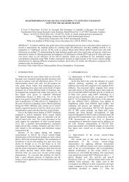
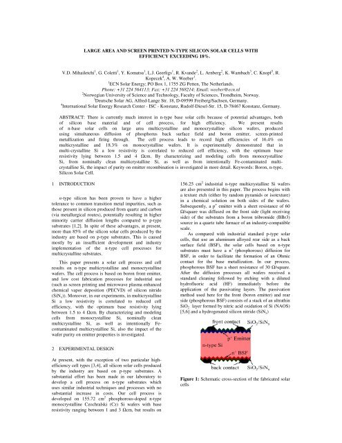
LARGE AREA AND SCREEN PRINTED N-TYPE SILICON SOLAR CELLS WITHEFFICIENCY EXCEEDING 18%.V.D. Mihailetchi 1 , G. Coletti 1 , Y. Komatsu 1 , L.J. Geerligs 1 , R. Kv<strong>and</strong>e 2 , L. Arnberg 2 , K. Wambach 3 , C. Knopf 3 , R.Kopecek 4 , A. W. Weeber 1 .1 ECN Solar Energy; PO Box 1, 1755 ZG Petten, The Netherl<strong>and</strong>s.Phone: +31 224 564113; Fax: +31 224 568214; Email: weeber@ecn.nl2 Norwegian University of Science <strong>and</strong> Technology, Faculty of Sciences, Trondheim, Norway.3 Deutsche Solar AG, Alfred-Lange Str. 18, D-09599 Freiberg/Sachsen, Germany.4 International Solar Energy Research Center - <strong>ISC</strong> - <strong>Konstanz</strong>, Rudolf-Diesel-Str. 15, D-78467 <strong>Konstanz</strong>, Germany.ABSTRACT: There is currently much interest in n-<strong>type</strong> base <strong>solar</strong> <strong>cells</strong> because of potential advantages, bothof <strong>silicon</strong> base material <strong>and</strong> of cell process, for high efficiency. We present resultsof n-base <strong>solar</strong> <strong>cells</strong> on <strong>large</strong> <strong>area</strong> multicrystalline <strong>and</strong> monocrystalline <strong>silicon</strong> wafers, producedusing simultaneous diffusion of phosphorus back surface field <strong>and</strong> boron emitter, <strong>screen</strong>-<strong>printed</strong>metallization <strong>and</strong> firing through. The cell process leads to record high efficiencies of 16.4% onmulticrystalline <strong>and</strong> 18.3% on monocrystalline wafers. It is experimentally demonstrated that inmulti-crystalline Si a low resistivity is correlated to reduced cell efficiency, with the optimum baseresistivity lying between 1.5 <strong>and</strong> 4 Ωcm. By characterizing <strong>and</strong> modeling <strong>cells</strong> from monocrystallineSi, from nominally clean multicrystalline Si, as well as from intentionally Fe-contaminated multicrystallineSi, the impact of purity on emitter recombination is investigated in more detail. Keywords: Boron, n-<strong>type</strong>,Silicon Solar Cell.1 INTRODUCTIONn-<strong>type</strong> <strong>silicon</strong> has been proven to have a highertolerance to common transition metal impurities, such asthose present in <strong>silicon</strong> produced from quartz <strong>and</strong> carbon(via metallurgical routes), potentially resulting in higherminority carrier diffusion lengths compared to p-<strong>type</strong>substrates [1,2]. In spite of these advantages, at present,more than 85% of the <strong>silicon</strong> <strong>solar</strong> <strong>cells</strong> produced by theindustry are based on p-<strong>type</strong> substrates. This is causedmostly by an insufficient development <strong>and</strong> industryimplementation of the n-<strong>type</strong> cell processes formulticrystalline substrates.This paper presents a <strong>solar</strong> cell process <strong>and</strong> cellresults on n-<strong>type</strong> multicrystalline <strong>and</strong> monocrystallinewafers. The cell process is based on boron front emitter,<strong>and</strong> low cost fabrication processes for industrial use(such as <strong>screen</strong> printing <strong>and</strong> microwave plasma enhancedchemical vapor deposition (PECVD) of <strong>silicon</strong> nitride(SiN x )). Moreover, in our experiments, in multicrystallineSi a low resistivity is correlated to reduced cellefficiency, with the optimum base resistivity lyingbetween 1.5 to 4 Ωcm. By characterizing <strong>and</strong> modeling<strong>cells</strong> from monocrystalline Si, nominally cleanmulticrystalline Si, as well as intentionally Fecontaminatedmulticrystalline Si, also the impact of thewafer purity on emitter properties is investigated.156.25 cm 2 industrial n-<strong>type</strong> multicrystalline Si wafersare also presented in this paper. The process begins witha texture etch (either by r<strong>and</strong>om pyramids or isotexture)in a chemical solution on both sides of the wafers.Subsequently, a p + emitter with a sheet resistance of 60Ω/square was diffused on the front side (light receivingside) of the substrates from a boron tribromide (BBr3)source in a quartz tube furnace of an industry-compatiblescale.As compared with industrial st<strong>and</strong>ard p-<strong>type</strong> <strong>solar</strong><strong>cells</strong>, that use an aluminum alloyed rear side as a backsurface field (BSF), the <strong>solar</strong> <strong>cells</strong> based on n-<strong>type</strong>substrates must have a n + (phosphorous) diffusion forBSF, in order to facilitate the formation of an Ohmiccontact for the base metallization. In our process,phosphorous BSF has a sheet resistance of 30 Ω/square.After the diffusion processes all wafers received ast<strong>and</strong>ard cleaning followed by etching with a dilutedhydrofluoric acid (HF) immediately before theapplication of the passivating layers. The passivationmethod used here for the front (boron emitter) <strong>and</strong> rearside (phosphorous BSF) consists of a stack of an ultrathinSiO 2 layer formed by nitric acid oxidation of Si (NAOS)[5,6] <strong>and</strong> a hydrogenated <strong>silicon</strong> nitride (SiN x )2 EXPERIMENTAL DESIGNAt present, with the exception of two particular highefficiencycell <strong>type</strong>s [3,4], all <strong>silicon</strong> <strong>solar</strong> <strong>cells</strong> producedby the industry are based on p-<strong>type</strong> substrates. Asubstantial effort has been made in our laboratory todevelop a cell process on n-<strong>type</strong> substrates whichuses similar industrial techniques <strong>and</strong> processes with nosubstantial increase in costs. Our cell process isdeveloped on 155.72 cm 2 phosphorous-doped n-<strong>type</strong>monocrystalline Czochralski (Cz) Si wafers with baseresistivity ranging between 1 <strong>and</strong> 3 Ωcm, but results onFigure 1: Schematic cross-section of the fabricated <strong>solar</strong><strong>cells</strong>
Table I: Comparison of the best <strong>solar</strong> cell parametersmeasured under st<strong>and</strong>ard test conditions (AM1.5G, 100mW/cm 2 , 25 o C). The <strong>solar</strong> <strong>cells</strong> were fabricated on156.25 cm 2 multicrystalline Si substrates <strong>and</strong> 155.72 cm 2monocrystalline Cz Si. The average efficiency of the 10monocrystalline <strong>cells</strong> with r<strong>and</strong>om pyramids texture etchwas 17.9%. The base resistivity is 1.8 Ωcm for themulticrystalline <strong>cells</strong> <strong>and</strong> 1.5 Ωcm for the Cz <strong>cells</strong>.WaferSurfacetextureJ sc[mA/cm 2 ]V oc[mV]FF[%]η[%]mc-Si isotexture 35.2 607 76.7 16.4Cz isotexture 36.3 629 75.8 17.3Cz r.pyramids 37.3 630 77.8 18.3Figure 2: Carrier concentration profile for boron(emitter) diffusion measured by ECV method on apolished Cz Si wafer.antireflection coating layer deposited by PECVD [7]. Thecell process is completed with <strong>screen</strong> printing of the front<strong>and</strong> back contacts followed by a co-firing step in order tobe able to make Ohmic contact between <strong>printed</strong> metalcontacts <strong>and</strong> Si. A schematic layout of the fabricated<strong>solar</strong> <strong>cells</strong> is shown in Figure 1.Figure 2 shows the resulting boron (emitter) dopingprofile measured on a polished Cz n-<strong>type</strong> test wafer,using the Electrochemical Capacitance-Voltage (ECV)method at <strong>ISC</strong> in <strong>Konstanz</strong>. The ECV measurementsreveal a doping profile of boron emitter up to 0.25 µmdepth with a visible surface depletion region. Thisdepletion is caused by the in-situ oxidation performed toremove the boron rich layer. Further optimization seemsto be needed in order to avoid this depletion region,which could enhance surface recombination of theminority charge carriers in the p + emitter because of anunfavorable electric field direction.3 RESULTS AND D<strong>ISC</strong>USSION3.1 Mono- <strong>and</strong> multi-crystalline cell resultsTable I shows the best <strong>solar</strong> cell parameters, obtainedusing the process described above, on multi- <strong>and</strong> monocrystalline<strong>silicon</strong> wafers. These measurements werecarried out under the st<strong>and</strong>ard test conditions using aclass A <strong>solar</strong> simulator. As can be seen from the table, aconversion efficiency of 16.4% is achieved on multicrystallinen-<strong>type</strong> substrates <strong>and</strong> nearly 1% absolutehigher efficiency on monocrystalline Cz substrate. Withthe difference coming from short-circuit current (J SC ) <strong>and</strong>open-circuit voltage (V OC ) it suggest that bulk lifetimemay still be an important limitation for multicrystalline n-<strong>type</strong> <strong>cells</strong>. A more quantitative analysis will follow laterin this paper.Nevertheless both, mono- <strong>and</strong> multicrystalline, cellefficiencies of table I represent the highest valuesreported for an n-<strong>type</strong> industrial process using <strong>screen</strong><strong>printed</strong><strong>and</strong> fired-through metallization on <strong>large</strong> <strong>area</strong>substrates (exceptions are the high-efficiency cellconcepts of Sunpower <strong>and</strong> Sanyo [3,4]). This represents asignificant step forward for industrial production of <strong>solar</strong><strong>cells</strong> based on n-<strong>type</strong> substrates. Moreover, furtherimprovements are expected (especially in the fill factor)for <strong>solar</strong> <strong>cells</strong> processed on isotexture etched surface. Wehave explored the benefits of this n-<strong>type</strong> process over themore developed <strong>and</strong> widely applied p-<strong>type</strong> process, <strong>and</strong>work is underway to industrialize the n-<strong>type</strong> process.3.2 Effect of base resistivityIn the following we have investigated <strong>solar</strong> <strong>cells</strong>fabricated on wafers belonging to different n-<strong>type</strong> multicrystallineSi ingots with difference in their baseresistivity, with the purpose to find out the optimumresistivity range for n-<strong>type</strong> multi-crystalline Si ingots <strong>and</strong><strong>cells</strong>. Two multicrystalline n-<strong>type</strong> ingots grown in thesame furnace have been selected for this investigation: acompensated ingot (called ingot 5) which is partially p-<strong>type</strong> (boron) <strong>and</strong> partially n-<strong>type</strong> (antimony) doped.Such a compensated ingot is very well suited for this <strong>type</strong>of investigation as it allows for a <strong>large</strong> variation in waferresistivity on a narrow part of the ingot size, whilevariation in concentration of metal impurities <strong>and</strong> crystaldefects is relatively small. The other n-<strong>type</strong> ingot (calledingot 6 /antimony doped) that we have investigated hasresistivity ranging from 2.2 to 0.3 Ωcm from bottom totop of the ingot. Solar <strong>cells</strong> have been fabricated (usingthe process described above) on 156.25 cm 2 wafersdistributed to cover a resistivity range of 0.8 to 7.7 Ωcmfrom ingot 5 <strong>and</strong> 0.3 to 2.2 Ωcm from ingot 6.Figure 3: Experimental power conversion efficiency η<strong>and</strong> J SC ×V OC product versus base resistivity of bothmulticrystalline n-<strong>type</strong> Si ingots investigated.
Figure 4: Minority carrier lifetime in the bulk τ bdetermined from the PC1D fit of IQE data as a functionof wafer base resistivity.Figure 3 shows the experimental conversionefficiencies (η) <strong>and</strong> J SC ×V OC product as a function of baseresistivity for both ingots investigated. As seen from thefigure the best results are obtained for wafers belongingto ingot 6, with the highest performance obtained around25% from the bottom of the ingot. The parameters of thebest cell measured are shown in table I. Anotherinteresting result that can be observed in figure 3 is thatthe J SC ×V OC product continues to rise for <strong>cells</strong> made fromingot 6 as resistivity is increased while it stays ratherconstant for <strong>cells</strong> of ingot 5 for resistivities <strong>large</strong>r than1.3 Ωcm. Above 3.5 Ωcm a decrease in η of ingot 5 is,however, caused by a decrease in FF. This decrease in FFis a result of a higher series resistance. Nevertheless, weshow that the optimum base resistivity for n-<strong>type</strong>multicrystalline Si feedstock lies between 1.5 to 4 Ωcm(these values can be lower if thinner wafers are produced)in order to maximize the efficiency output throughout theingot.Figure 4 shows the bulk lifetime (τ b ) resulting fromfitting the internal quantum efficiencies (IQE) data of the<strong>cells</strong> from both ingots investigated. From lifetime data itis observed that a resistivity higher than approximately1.3 Ωcm is required in order to ensure that bulk diffusionlength L d,bulk >W (W is the averaged wafer thickness of allinvestigated <strong>cells</strong>) for both ingots. For L d,bulk 85% towards the top of ingot 5. Notably, the lifetime asa function of resistivity shows for low resistivity a lineardependence, suggesting activity of some impurity whichis relatively harmful in n-<strong>type</strong> base (e. g. Au, Zn, perhapsCr) [1,8,9].3.3 Effect of impurities on emitter recombinationWhile the n-<strong>type</strong> base of the <strong>solar</strong> <strong>cells</strong> may beexpected to be less sensitive to many transition metalimpurities, the p + emitter could rather be more sensitive.It is commonly believed that recombination into thehighly doped emitter region is dominated by Auger <strong>and</strong>radiative recombination. Recent investigations, however,show that relatively <strong>large</strong> amounts of metal impurities(e.g., Fe, Cu, Cr) can be gettered in a n + (phosphorous)emitter duringFigure 5: Front (empty symbols) <strong>and</strong> rear side (semifilledsymbols) IQE of <strong>solar</strong> <strong>cells</strong> fabricated from amono-crystalline (Cz) ingot, a reference multi-crystalline,<strong>and</strong> a multi-crystalline ingot with 50 ppmw of Fe. Thesolid lines represent the PC1D calculation consideringthe emitter recombination parameters from table II.diffusion processes [10]. These gettered impurities haverelatively low impact on a n + emitters due to their highercapture cross-section of electrons as compared withholes.In order to verify that metal contamination of the p +emitters can indeed have a significant effect, n-<strong>type</strong> <strong>solar</strong><strong>cells</strong> were fabricated (using the process described in thispaper) from clean monocrystalline (Cz) wafers,nominally clean multicrystalline Si wafers, <strong>and</strong> multicrystallineSi wafers from feedstock intentionallycontaminated with 50 ppmw of Fe [11]. The resultingIQE <strong>and</strong> I−V data were modeled using PC1D simulationprogram taking into account measured front <strong>and</strong> reardoping profiles, surface reflection, base resistivity, <strong>and</strong>wafer thickness. The relevant fit parameters left for themodeling are τ b , front <strong>and</strong> rear surface recombinationvelocities (SRV), <strong>and</strong> emitter recombination. The latterparameter has been introduced in our PC1D model as aseparate emitter region with an effective diffusion length(L d,emitter ) taken at an acceptor density of N A =10 20 cm −3 .By fitting both front <strong>and</strong> rear IQE data all fit parameterscan readily be determined. The results show that only τ b(or L d,bulk ) <strong>and</strong> L d,emitter needs to be varied betweenvarious <strong>cells</strong> with a constant front SRV of 1.0(±0.5)×10 4cm/s (on boron emitter) <strong>and</strong> rear SRV of 1.0(±1)×10 5cm/s (on phosphorous BSF). A constant SRV isexpected since all <strong>solar</strong> <strong>cells</strong> have been processed in thesame run.Figure 5 shows the experimental IQE curves(symbols) of selected <strong>cells</strong> from the three different ingotstogether with the PC1D fit using the model discussedabove. The front IQE clearly does not indicate a variationin front surface passivation. However, without includingrecombination active defects in the emitter(L d,emitter >>W emitter ), the PC1D calculated V OC <strong>and</strong> theexperimental V OC of the <strong>cells</strong> deviate significantly. Thedeviation varies from 6 mV for the Cz wafer, to 22 mVfor the Fe-contaminated wafer. This deviation can befitted well (without affecting the IQE curves) byincluding interstitial Fe defects into the p + emitter. Ofcourse, interstitial Fe is a likely contaminant that canaffect the diffusion length in the emitter, but also other
Table II: PC1D fit parameters used in figure 5. L d,emitteris taken at N A =10 20 cm −3 , whereas ∆V OC represents thedifference between calculated V OC , when only Augerrecombination is considered in the emitter, <strong>and</strong> measuredV OC of the <strong>cells</strong>.Waferequiv.L d,bulk L d,emitter∆VFe OC[µm] [µm]i[cm −3 [mV]]Cz 841 0.56 9×10 14 6mc-Si(reference)284 0.47 2×10 15 14mc-Si(50 ppmw Fe)192 0.41 4×10 15 22impurities may be present. Thus, the interstitial Feconcentration is used here as a convenient parameter torepresent increased Schockly-Read-Hall emitterrecombination in general. The resulting fit parameters areshown in table II. It was found that consideration of thiscontamination was essential to simultaneously fit IQEcurves as well as V OC correctly . Incidentally, it can beseen that the 50 ppmw of Fe have only modest effect onL d,bulk of the <strong>solar</strong> <strong>cells</strong> but it can bring significantlimitation to V OC due to the emitter contamination.Further analysis of this effect is in progress.Based on fitted IQE of different multicrystalline <strong>and</strong>monocrystalline <strong>cells</strong> <strong>and</strong> using our model calculation wewere able to identify the efficiency enhancementpossibility for our n-<strong>type</strong> cell process. Figure 6 showsthe experimental efficiencies of the <strong>cells</strong> of figure 5.These efficiencies are plotted together with the calculatedcurve against the ratio of minority carrier diffusion lengthin the bulk <strong>and</strong> wafer thickness (L d,bulk /W), assuming anisotexture etched surface, same metallization shadowing,FF, <strong>and</strong> W, for all <strong>cells</strong>. A good agreement is observedfor all <strong>cells</strong> allowing us to quantify the relation betweenmaterial quality (given by L d,bulk ) <strong>and</strong> the resulting <strong>solar</strong>cell efficiency when all other parameters of the processare the same. Work is underway to elucidate the relationbetween L d,bulk <strong>and</strong> the presence of some defects in mc-Siwafers [11].4 CONCLUSSIONWe have demonstrated a process to fabricate n-<strong>type</strong><strong>solar</strong> <strong>cells</strong> on <strong>large</strong> <strong>area</strong> (156.25 cm 2 ) multicrystalline <strong>and</strong>mono-crystalline Cz substrates, involving diffusion ofphosphorus BSF <strong>and</strong> boron emitter, <strong>screen</strong>-<strong>printed</strong>metallization <strong>and</strong> firing through, leading to efficiencies of16.4% on multicrystalline Si <strong>and</strong> 18.3% on Cz.Experiments on wafers of different base resistivity showthat the optimum target resistivity for n-<strong>type</strong>multicrystalline <strong>silicon</strong> wafers lies between 1.5 to 4 Ωcmin order to maximize the efficiency output thorough theingot. In multicrystalline <strong>cells</strong>, modeling gives a clearindication that contaminants inside the wafer affect theemitter recombination.ACKNOWLEDGEMENTSThis work was supported by the EuropeanCommission within the FoXy project under the contractnumber 019811(SES6), <strong>and</strong> by the Dutch agency forenergy <strong>and</strong> the environment SenterNovem. ECNacknowledges cooperation with Tempress.REFERENCES[1] D. MacDonald, L. J. Geerligs, Appl. Phys. Lett. 85,4061 (2004).[2] J. E. Cotter et. al., 15 th Workshop on CrystallineSilicon Solar Cells & Modules: Materials <strong>and</strong> Processes,p. 3 (2005).[3] M. Taguchi, A. Terakawa, E. Maruyama, M. Tanaka,Progr. Photovolt. 13, 481 (2005)[4] K. R. McIntosh, Proc. of the 3 rd World Conf. onPhotovoltaic Energy Conversion, p. 971 (2003).[5] Asuha, S. Imai, M. Takahashi, H. Kobayashi, Appl.Phys. Lett. 85, 3783 (2004).[6] Asuha, Y. Liu, O. Maida, M. Takahashi, H.Kobayashi, J. Electrochem. Soc. 151, 824 (2004).[7] V. D. Mihailetchi, Y. Komatsu, L. J. Geerligs, Appl.Phys. Lett. 92, 063510 (2008).[8] L. J. Geerligs <strong>and</strong> D. H. Macdonald, Progr.Photovolt. 12, 309 (2004).[9] J. Schmidt et al., Proc. of the 22 nd EuropeanPhotovoltaic Solar Energy Conf., p. 998 (2007).[10] A. Bentzen, A. Holt, R. Kopecek, G. Stokkan,J. S. Christensen, B. G. Svensson, J. Appl. Phys.99, 093509 (2006).[11] G. Coletti, R. Kv<strong>and</strong>e, V. D. Mihailetchi, L. J.Geerligs, L. Arnberg, E. J. Øvrelid, J. Appl. Phys. (to bepublished).Figure 6: Calculated (solid line) <strong>and</strong> experimental(symbols) efficiency as a function of minority carrierdiffusion length <strong>and</strong> wafer thickness ratio (L d,bulk /W).