NEW GENERATION BEACON DRIVER - G4JNT
NEW GENERATION BEACON DRIVER - G4JNT
NEW GENERATION BEACON DRIVER - G4JNT

Create successful ePaper yourself
Turn your PDF publications into a flip-book with our unique Google optimized e-Paper software.
Message StructureIn normal usage JT65 relies on automatic timing control, making use of a one minute transmit / one minute receivesequence which has to be replicated in the receiver’s computer. The timing is allowed to be in error by up to four secondslate or one second early when referred to the transmission. The rest of the beacon's timing is based on a thirty secondtime-slot structure which determines the data transmission pattern for the whole beacon sequence. As the JT65transmissions must be aligned with the minute, timeslots must be set and allocated accordingly. Time information sentfrom the GPS receiver is used to derive a number of 30 second time slots, referenced to the hour, and any even number ofup to 16 slots can be programmed with different data formats allocated to each 30s slot. Changes are made by modifyingthe PIC code for the beacon controller. For a typical transmission sequence, JT65 will be allocated to every fourth slot(starting at an even number), to give the one minute + one minute cycle of transmission periods. As a JT65 transmissionperiod lasts 48 seconds it will run into the next 30s time, so this one cannot be allocated to any other mode. The rest of theslots can be allocated to CW, Carrier, BPSK or RTTY as needed. To avoid sequence breaks on the hour, the number ofslots used should ideally be a submultiple of 120, so values of 2,4,6,8,10,12 are the most convenient, corresponding to 1 to6 minute repeat cycles. The number of minutes for the cycle is specified in the setup information.Any CW or RTTY transmission will be of arbitrary length, and the remaining time up to the end of their timeslot isautomatically taken up with plain carrier. If a CW or RTTY data exceeds 30s in length, the data for the following timeslotwill be ignored.Although the second 30 second slot after a JT65 transmission is ignored, it should be defined in the sequence definition.This is because JT65 is not transmitted when the GPS receiver has lost lock. The first time slot allocated to JT65 defaults,instead, to the first CW message and the second time slot is as defined in the setup data. When GPS lock is restored, JT65operation resumes and the second time slot definition is then ignored.As implemented on GB3VHF the sequence programmed is :00:00 JT65 sending the message “GB3VHF JO01DH”00:30 CW message as below (only sent during Invalid GPS)01:00 CW Message “GB3VHF JO01DH” (approx 13 seconds) followed by plain carrier01:30 Phase reversals at one second intervals.Repeated every two minutesAs far as a listener is concerned, starting on the even minute boundary, this appears as :48 seconds of JT65 transmission12 seconds of plain carrier13 seconds of CW Ident17 seconds of plain carrier30 seconds of phase reversals- Sequence repeats---------------------------------------------------------------------------------------------------------------------------DDS and Controller HardwareThe driver unit comprises several modules working together under the control of a single 16F628 PIC microcontroller.The DDS is clocked from a reference input, and a Phase Locked Loop on board the AD9852 multiplies this by aprogrammed value from 4 to 20, for a maximum allowed clock frequency of 300MHz. In this VHF-band beacon driver, areference input of 12.8MHz is multiplied by 16 in the PLL for a 204.8MHz clock. Keeping the clock below the 300MHzmaximum permitted in the AD9852 specification results in a lower power consumption and improves reliability of the DDSchip. The 12.8MHz reference oscillator is derived from a Voltage Controlled, Temperature Compensated CrystalOscillator (VTCXO) which in turn is phase locked to the 10kHz output from a Jupiter TU-60 GPS receiver module.The microcontroller, mounted on the same PCB as the DDS chip, communicates with the GPS receiver in order to read thetime of day (UTC) and the GPS receiver / satellite status information. The 1 Pulse Per Second (1PPS) signal generated bythe GPS receiver is fed to the PIC in order to generate accurate timing – the 1PPS signal is typically accurate to within200ns of UTC. The PIC uses the data from these two signals to accurately set the start and stop times of the variousmodulations transmitted.Page 2
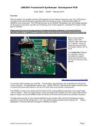
By writing suitable software for the PIC, a wide range of modulation types can be generated by reprogramming the DDSchip with new frequency, amplitude or phase information at regular intervals.Frequency ReferenceThe TCXO output is divided by 1280 to give a 10kHz output. An exclusive–OR gate compares this with the 10kHz outputfrom the GPS receiver to generate a feedback signal for the Phase Locked Loop. An analogue switch controlled from thePIC opens the feedback loop if the GPS receiver is not locked up, forcing the TCXO to run at a fixed frequency. Thisprevents gross frequency errors as a result of a free-running GPS receiver. The PIC continuously monitors the receiverstatus and controls this analogue switch when the data from the GPS receiver indicates that the status is satisfactory, ie. thatit has locked up. The phase-locked loop has a time constant of 4 seconds, so there is a noticeable ‘blip’ as this controlsignal switches to its active state and the PLL begins to lock up. Frequency stability will be achieved about 30 seconds to 1minute after the GPS receiver has locked up.Driver Hardware and ConstructionThe three PCBs making up the assembly are mounted in a single diecast box. The DDS and PIC assembly is fixed abovethe GPS receiver and frequency reference boards to give easy access to the PIC for reprogramming. Two voltageregulators, 3.3V for the DDS and 5V for the GPS receiver and divider assembly, are mounted on the side of the box with anadditional heatsink on the outside. (The PIC on the DDS board has its own low power 5V regulator). The DDS chipconsumes around 650mA during operation and runs quite hot. Its main heatsinking mechanism normally consists ofconducting heat away from the base of the chip through the PCB, but here no air flow is possible inside the diecast box soadditional chip cooling has to be provided. A sprung copper strip conducts heat away from the top of the DDS chip to theside of the diecast box, the strip presses onto the top of the AD9852, with thermal grease added to ensure heat conductivity.At a room temperature of 20C, the voltage regulator heatsink sits at around 34C, the black painted surface of the diecastbox at 28C, and the chip is estimated to sit at around 40C - without the copper strip, it was closer to 55C. When thediecast box is mounted on a metal baseplate giving further conduction cooling, all the temperatures drop proportionately.Interfacing and ConnectionsFive signal / power connections are provided on feedthrough capacitors:DC POWERNO GPSRequires a voltage greater than 8V and internal linear regulators take this down to 5 / 3.3V. Currentconsumption is approximately 0.8 to 0.9A. To avoid excessive heat generation, avoid using a supplyvoltage much greater than 12V – use an external dropper resistor if necessaryGoes high when the GPS receiver has not acquired lock; it is pulled to +5V via a 2k2 resistor and can beused to directly drive an LED. A high brightness type is advisable due to the limited current availablefrom this pin.RED LED + GRN LEDThese are intended to drive a bi-directional (antiphase connected) two-colour LED ‘CONTROLLERSTATUS’. The pattern of flashing / colours on this is determined in software and used to indicate thestatus of the DDS controller software. Each pin is driven from a 5V source/sink via a 150 ohm resistor.The positive side of each colour goes to the pin labelled.TEST MODEis an input pin which is left open-circuit for normal operation. When shorted to ground, the controllerenters carrier-only mode as soon as the current transmission interval has completed and stays there untilthe short is removed. Its function is to allow for frequency setting / measurement, and for testing theadditional RF hardware.Bi-Colour LED Flashing CodesAs implemented, the LED flash codes are :When power is first applied to the driver, the LED flashes three times Red/Green alternately each second.Before the GPS receiver has locked up, or if the GPS receiver loses signal:Page 3
The Green LED gives a short flash once per second while carrier-only is being transmitted.The Red LED flashes in sympathy with the CW characters when CW is being sentAlternate Red/Green flashes for the BPSK mode, once per second corresponding to each phase stateWhen lockup has been achieved and the beacon is operating normally :The Green LED gives a long flash once per second while carrier-only is being transmitted.The Red LED flashes in sympathy with the CW characters when CW is being transmitted.Alternate Red/Green flashes for the BPSK mode, once per second corresponding to each phase stateFor the JT65 transmission, the LED flashes Red at the JT65 symbol rate of 2.7Hz---------------------------------------------------------------------------------------------------------------------------Frequency Doubler and Output Buffer.At the 204.8MHz clock frequency of the DDS chip, the maximum frequency that can be generated by the AD9852 chip isaround 80MHz. A 5 th order elliptic filter on the PIC output, mounted on the DDS board, reduces alias and harmonicproducts to at least 50dBc A frequency doubler built in a separate module is used to generate the final 144MHz output,The output from the DDS board is amplified to a level of approximately 11dBm and feeds a push-pull diode doublercircuit. This provides 40dB rejection of the fundamental and is followed by a two section bandpass filter that ensures allspurii are at a level of at least 55 dBc. Two stages of amplification raise the filter output to a level of 12.5dBm with thefinal modamp running at 1 - 2dB of gain compression. The buffer has no harmonic filtering on its output so if the doubleris to be followed by broadband amplification, extra harmonic filtering will be needed.All amplifier stages consist of MAR-3 and MAR-4 modamps supplied from constant current regulators to give immunityfrom supply voltage and temperature variations. Any supply voltage from 9 to 13V is acceptable. The doubler / bufferassembly is constructed in a screened tinplate box with SMC connectors for the RF, and a feedthrough capacitor for thesupply voltage.---------------------------------------------------------------------------------------------------------------------------User ProgrammingFrequency information (the codes that need to be sent to the DDS chip) together with the text of the various messages arestored in the EEProm memory area of the PIC. The boundaries of the various messages need to be known by theassembler, so it is not possible to reprogramme the EEProm contents alone if the length of any of the messages have beenchanged. In general it is safer to re-assemble the whole file and re-programme the entire PIC device – this should take lessthan one minute for most PIC programmers. Any change to the message sequence, or time slot allocation, must involve acomplete re-programming of the PIC.Frequency and message contents are contained in a separate include file (VHFBCNE2.INC) which can be edited on its own.A total of 128 bytes of storage is available, and of this the first 30 bytes are used for frequency data, leaving 98 bytes forstorage of all the characters needed for all the messages.The frequency information (DDS codes) can conveniently be generated from an accessory programme calledVHFBCNCALCS.EXE. See Annex A for an example of this utility. The programme generates a file which includes linesof PIC code that can be directly cut and pasted into VHFBCNE2.INC. See the example below. The include file also hasother constants used within the programme, such as RPTTime - the number of minutes (pairs of time slots) for thetransmission sequence; CWSPEED (the CW dot length in milliseconds) for the CW messages; and the RTTY baud ratedefined in units of 500µs. It is convenient to let the assembler calculate this value for you, by dividing 2000 by a specifiedbaud rate. The constant NMEAPol, shown in the example, is not applicable to this software, but is needed in other PICsoftware that makes use of the same include file.Note that the DDS controller software here does not make use of the carrier frequency itself. Instead, the following valuesare stored in EEProm to produce the required frequencies from the specified clock:The absolute JT65 Sync frequencyThe increment between tonesGenerates a tone of 11025 / 1024 * 118 ≈ 1270.5Hz in an SSBreceiver tuned to the specified carrier frequency.11025/4086 * M where M is 1 for JT65A, 2 for JT65B and 4 forJT65C. For JT65B the increment is approximately 5.38Hz The PICsoftware then calculates the frequency data to be sent to the DDS bymultiplying this value of increment by a number between 2 and 65Page 4
depending on the character to be sent, then adding the result to thevalue for the sync tone.The Centre frequency for CW and carrierRTTY MarkRTTY SpaceCorresponds to a tone frequency as shown - an 1500Hz value isshown in VHFBCNE2.INC below).1275 Hz Tone1445 Hz ToneIf the DDS output is subsequently frequency-multiplied, all the values are modified by the multiplication factor.Frequency codes are stored in EEPROM in the order high byte to low byte so the full numerical value can more easily beseen from the individual data in a listing.As an example, take the sync tone which has a hexadecimal value of 0x5A44C365E354This value can be converted back to the actual frequencies, as follows:Convert hex number to decimal N = 99251382510420 (10)Divide by 2 48 N / 2 48 = 0.352611744Multiply by the DDS clock frequency N / 2 48 * 204.8MHz = 72.21488523 MHzand finally by the RF multiplication … * 2 = 144.42977046 MHzie. 1270.46Hz above the suppressed carrier at 144.4285MHzAll message contents are stored in the 128 bytes of user EEprom. Text messages must be terminated with a null characterto indicate their end, but as the pre-coded data for the JT65 transmission take up exactly 63 spaces, it is therefore selfterminating. The various labels of the form JTMSGOFFSET = $ - 0x2100 are an essential part of the software and mustbe correctly placed immediately before the start of each character string. If EEProm storage becomes full, it is allowable toreuse strings between different messages. In this event, either the main body of the assembler code needs to be changed sothe data-sending subroutines point to the appropriate data label, or more conveniently, both labels can be placed at the samepoint.The assembler include file, VHFBCNG2.INC , contains the allocation of message type to timeslot. Up to 16 GOTOstatements cause the PIC code to jump to the appropriate section of code for each time slot. Although only sufficientGOTOs need to be included to cope with the value of RPTTime defined in VHFBCNE2.INC, it is safer to include sufficientjumps to cope with the maximum number of slots that could conceivably be allocated – setting an incorrect value forRPTTime will cause havoc with the PIC code if a jump is not in the correct place! Any mistakes or typing errors madewhen changing this file will usually (hopefully !) show as errors when assembled. Error messages will not necessarily begenerated if incorrect values appear in the ..E2 file, as the assembler cannot identify many numerical and memoryallocation errors.Page 5
ZorglidmaatschapMet het oog op de toekomst zoeken vele mensen naar een zorgzekerheid voor hetgeval dat zij plotseling worden geconfronteerd met ziekte of het niet meer alleenkunnen zijn.Menigeen vraagt zich af of het mogelijk is om zich bij Care Company Thuiszorg aante sluiten om zo van zorg verzekerd te kunnen zijn.Care Company heeft deze mogelijkheid gecreëerd in de vorm van eenzorglidmaatschap.Wat houdt een zorglidmaatschapbij Care Company in?Hoe wordt ik lid?U meldt zich aan via de website van Care Company, per post of telefoon en wijsturen u een brochure toe met daarbij ingesloten een aanmeldingsformulier. Hierkunt u in alle rust over nadenken voordat u het eventueel invult. Na ongeveer 2weken nemen wij contact met u op voor het maken van een vrijblijvende afspraakom alles met u door te nemen.Uw gegevens worden met uiterste zorgvuldigheid en volgens de Wet BeschermingPersoonsgegevens bewaard.U bent na uw inschrijving bekend bij ons en wij zijn op de hoogte van uw wensen.Op het moment dat u ons nodig heeft is 1 telefoontje genoeg om alle raderen aanhet werk te zetten om u te voorzien van de juiste zorg.ZorglidmaatschapMet een zorglidmaatschap bent u verzekerd van zorg zoals u dat wenst. Wij zijn opde hoogte van uw wensen en gegevens, zoals u die aan ons kenbaar heeft gemaakt.Wij kunnen u, indien nodig, direct van de juiste zorg voorzien. Wij nemen 1 maalin de 6 maanden contact met u op om op de hoogte te blijven van eventueleaanpassingen in uw wensen en om te vragen hoe het met u gaat!Regelen van uw zorg vanuit een gezonde situatieHet is belangrijk om vanuit een gezonde situatie uw zorg van te voren te kunnenregelen en vast te leggen zoals u dat wilt.Vooral als u het in geval van ziekte niet meer in staat bent om zelf duidelijk kanaangeven wat u wilt en vooral niet wilt.U zou om te beginnen kunnen denken aan:• Wie gaat mijn zaken regelen als ik het niet meer kan• Hoe zit mijn verzekering eigenlijk in elkaar qua kostenvergoeding• Wat wil ik wel en wat niet als ik ernstig ziek word• Heb ik alles wel goed verwoord en neergelegd bij mijn notaris• Wil ik wél of niet opgenomen worden in een verpleeghuis• Wil ik levensverlengende therapie• Wil ik gereanimeerd wordenLidmaatschapskostenDe lidmaatschapskosten voor 1 persoon of echtpaar bedragen totaal E 50,= per jaar.Als lid van Care Company ontvangt u een ledenkaart met daaraan verbondenvoordelen. Deze voordelen kunt u terug vinden op onze website.Voor het aanvragen van een lidmaatschap kunt u bellen met:Laren 035 - 5311880Amsterdam 020 - 6701800Den Haag 070 - 3897700Of u kunt zich opgeven via onze website: www.zorglidmaatschap.nlWij leveren meer dan zorg alleen!
Annex AVHFBcnCalcs.exeCalculation of frequency codes.The Windows software VHFBcnCalcs.exe allows a user to enter the DDS reference input frequency, PLL clockmultiplier,the RF carrier frequency, a tone for the centre (CW) keying and the RF multiplication after the DDS output.The software uses this data to calculate the frequency codes needed for the beacon driver; the user window is shown below.All codes are given in hexadecimal, preceded with 0x. If a file name is specified, the data will be written to this file in aformat suitable for cutting and pasting the lines of data directly into the PIC assembler code. The contents of a such anoutput file is shown below; compare the second part of this with the contents of VHFBCNE2.INC shown earlier.As well as the JT65 frequency codes (specifically, the sync tone and increment value) the software gives the values for theCW / continuous carrier frequency, and the RTTY mark and space frequencies corresponding to the standard 1275/1445Hztone shift. Although not implemented in this beacon driver, the four frequency codes corresponding to each of theequivalent FSK441 tones is also calculated for use in other beacon controller software (such as FSK441BC.ASM) as well asthe SSB carrier value itself. The values for the DDS control register are derived from the PLL multiplication factor andthe clock frequency; this information is needed in the DDS setup code. Finally, the data needed to be programmed into theDDS phase register to obtain a 180 degree phase shift is presented, taking takes into account the final RF multiplicationfactor.CONTENTS OF ‘GB3VHF’ FROM FTHE ‘ ‘VHFBcnCalcs’ utility.;AD9852 DDS register data for VHF/UHF beacons running WSJT Modes; Cut and paste into PIC assembly file;Frequency data;Fcarrier = 144.4285 , RF Mult = 2 , Fo(carrier) = 72.21425;Ref in = 12.8 , PLL Mult= 16 , Clock freq = 204.8de 0x5A,0x44,0xB3,0x7C,0x99,0xAF ; FSK441 Tone 0de 0x5A,0x44,0xC5,0x8C,0xD2,0x0B ; FSK441 Tone 1de 0x5A,0x44,0xD7,0x9D,0x0A,0x67 ; FSK441 Tone 2de 0x5A,0x44,0xE9,0xAD,0x42,0xC4 ; FSK441 Tone 3 Hzde 0x5A,0x44,0x8F,0x5C,0x28,0xF6 ; Carrier, Fode 0x5A,0x44,0xC3,0x65,0xE3,0x54 ;JT Sync tonede 0, 0, 0x00,0x70,0xE5,0x60 ;JT44 Tone Intervalde 0, 0, 0x00,0x38,0x72,0xB0 ;JT65B Tone Intervalde 0x5A,0x44,0xCC,0xCC,0xCC,0xCD ;1500Hz Tonede 0x5A,0x44,0xC3,0x95,0x81,0x06 ;RTTY Mark 1275 Hzde 0x5A,0x44,0xCA,0x8C,0x15,0x4D ;RTTY Space 1445 Hz;AD9852 Control reg 0x10,0x50,0x00,0x60 (OSK On);PHASE180 Constant 0x10,0x00Page 8
Annex BGenerating the data for the JT65 transmissionJT65CODE.EXE , J65TOPIC.EXE and GENJT65.EXEGeneration of the 63 coded symbols for any JT65 message is far too complex a procedure to be incorporated within thebeacon controller itself – involving message compression, interleaving and Reed-Solomon coding to turn the 13 charactertext into 63 codes corresponding to the transmitted tones. A utility called JT65CODE.EXE can be downloaded from theWSJT web site ( http://pulsar.princeton.edu/~joe/K1JT/Download.htm ), this is needed to generate the symbols that are tobe stored in EEPROM. The full source code for the utility can also be found here, and is invaluable for understanding theinner workings of the JT65 coding.The 63 code words are generated by typing JT65CODE “GB3VHF JO01DH” from a DOS prompt. Replace the textbetween the inverted commas with your 13 character message of choice. This instruction sends the result to the screen. Toget the result into the PIC listing, the data can either be captured from screen with a text capture utility, or the programmeoutput can be sent to a file by the DOS redirection utility (which still works, even under Windows NT) by typing :JT65CODE “GB3VHF JO01DH” > GB3VHFJT.TXTThe result is sent to the file named. An example of the output from JT65CODE is shown below.Message: gb3vhf jo01dhPlain text.Packed message, 6-bit symbols: 24 8 29 9 25 30 11 30 54 8 3623Channel symbols, including FEC:26 2 61 34 15 15 35 50 17 50 29 54 47 37 1 16 19 14 37 43 4718 41 40 39 20 17 63 43 59 8 50 57 50 12 45 7 45 12 18 2 409 19 12 33 11 2 49 10 40 48 13 54 24 20 46 25 24 49 60 21 28Decoded message: GB3VHF JO01DHThe symbols can now either be typed into the PIC assembler listing manually, or a second programme JT6TOPIC.EXE(available from <strong>G4JNT</strong>) can be used to convert the data into a form for direct pasting into the assembler file. To use thisutility (assuming the filename as generated above) type :J65TOPIC GB3VHFJT.TXTYou will be prompted for a destination file name, which will be generated containing the data in a form suitable for pastinginto VHFBCNE2.INCTypical output from J65TOPIC.EXE, as stored in the destinationfile suitable for directly pasting into VHFBCNE2.INCde d'26', d'2', d'61', d'34', d'15', d'15', d'35', d'50'de d'17', d'50', d'29', d'54', d'47', d'37', d'1', d'16'de d'19', d'14', d'37', d'43', d'47', d'18', d'41', d'40'de d'39', d'20', d'17', d'63', d'43', d'59', d'8', d'50'de d'57', d'50', d'12', d'45', d'7', d'45', d'12', d'18'de d'2' , d'40', d'9', d'19', d'12', d'33', d'11', d'2'de d'49', d'10', d'40', d'48', d'13', d'54', d'24', d'20'de d'46', d'25', d'24', d'49', d'60', d'21', d'28'; GB3VHF JO01DHUpdate Jan 2011The programme GENJT65.EXE combines the two stages by making the formatted call to Joe’s JT65CODE andgenerating the .INC file. Run GENJT65 and follow the instructions. Please note that you still need JT65CODE.EXE tobe present in the same directory as GENJT65.EXEPage 9
Annex CCircuit DiagramsPage 10
DDS Module Circuit Diagram (updated Jan 2011)Page 11
72 to 144MHz Frequency DoublerPage 12
Jupiter-T GPSReceiver moduleGPS DisciplinedOscillator /12.8MHz FrequencyreferenceRF Output(72.2MHz)GPSAntennainputHeatsinkingCu strip +Al platePIC 16F628MicrocontrollerAD9852 DDSFrequency Source72 to 144MHz Frequency DoublerPage 13