LPC2478 Developer's Kit - User's Guide - Embedded Artists
LPC2478 Developer's Kit - User's Guide - Embedded Artists
LPC2478 Developer's Kit - User's Guide - Embedded Artists

You also want an ePaper? Increase the reach of your titles
YUMPU automatically turns print PDFs into web optimized ePapers that Google loves.
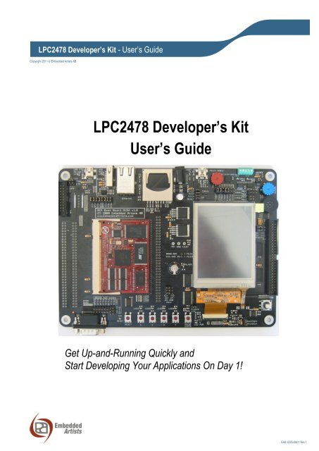
<strong>LPC2478</strong> Developer’s <strong>Kit</strong> - User‟s <strong>Guide</strong>Copyright 2011 © <strong>Embedded</strong> <strong>Artists</strong> AB<strong>LPC2478</strong> Developer’s <strong>Kit</strong>User’s <strong>Guide</strong>Get Up-and-Running Quickly andStart Developing Your Applications On Day 1!EA2-USG-0801 Rev I
<strong>LPC2478</strong> Developer’s <strong>Kit</strong> - User’s <strong>Guide</strong> Page 2<strong>Embedded</strong> <strong>Artists</strong> ABDavidshallsgatan 16211 45 MalmöSwedeninfo@<strong>Embedded</strong><strong>Artists</strong>.comhttp://www.<strong>Embedded</strong><strong>Artists</strong>.comCopyright 2005-2011 © <strong>Embedded</strong> <strong>Artists</strong> AB. All rights reserved.No part of this publication may be reproduced, transmitted, transcribed, stored in a retrieval system, ortranslated into any language or computer language, in any form or by any means, electronic,mechanical, magnetic, optical, chemical, manual or otherwise, without the prior written permission of<strong>Embedded</strong> <strong>Artists</strong> AB.Disclaimer<strong>Embedded</strong> <strong>Artists</strong> AB makes no representation or warranties with respect to the contents hereof andspecifically disclaim any implied warranties or merchantability or fitness for any particular purpose.Information in this publication is subject to change without notice and does not represent acommitment on the part of <strong>Embedded</strong> <strong>Artists</strong> AB.FeedbackWe appreciate any feedback you may have for improvements on this document. Please send yourcomments to support@<strong>Embedded</strong><strong>Artists</strong>.com.TrademarksAll brand and product names mentioned herein are trademarks, services marks, registeredtrademarks, or registered service marks of their respective owners and should be treated as such.Copyright 2011 © <strong>Embedded</strong> <strong>Artists</strong> AB
<strong>LPC2478</strong> Developer’s <strong>Kit</strong> - User’s <strong>Guide</strong> Page 3Table of Contents1 Document Revision History 52 Introduction 62.1 Features 62.2 ESD Precaution 72.3 General Handling Care 72.4 Code Read Protection 82.5 CE Assessment 82.6 Other Products from <strong>Embedded</strong> <strong>Artists</strong> 82.6.1 Design and Production Services 82.6.2 OEM / Education / QuickStart Boards and <strong>Kit</strong>s 93 <strong>LPC2478</strong> OEM Board Design 103.1 <strong>LPC2478</strong> OEM Board Schematics 103.1.1 CPU 103.1.2 Powering 103.1.3 Analog Inputs/Outputs 103.1.4 Ethernet Interface 103.1.5 External Memories 113.1.6 External Memory Interface 113.1.7 Reset Generation 113.1.8 I2C E2PROM 113.1.9 Expansion Connectors 123.2 Memory Layout 123.3 Usage of CPU Pins 123.4 <strong>LPC2478</strong> OEM Board Mechanical Dimensions and Connector 133.5 Known Limitation of <strong>LPC2478</strong> OEM Board 143.5.1 Ver 1.0 – SDRAM Clock Frequency 143.5.2 Ver 1.0 – Ethernet Clock 143.5.3 NAND FLASH Bad Block 143.5.4 Brand of Memory Chips 154 QVGA Base Board Design 164.1 Usage of CPU Pins 164.2 Known Limitation of QVGA Base Board 194.2.1 Version 1.0/1.1 – SD/MMC Interface Pullups 194.3 Jumpers 204.3.1 Default Jumper Positions 214.3.2 Illegal Jumper Combinations 214.4 Connectors 224.4.1 Mictor-38 ETM Connector 224.5 Important Components 235 Getting Started 24Copyright 2011 © <strong>Embedded</strong> <strong>Artists</strong> AB
<strong>LPC2478</strong> Developer’s <strong>Kit</strong> - User’s <strong>Guide</strong> Page 45.1 Demo Applications 245.1.1 Custom Slideshow Demo Application #3 245.2 Initial Setup and Powering 265.3 Getting Started with uClinux 285.3.1 Basic Requirements 285.3.2 LAN/Ethernet Setup 285.4 FTDI USB Driver Installation 305.4.1 USB Driver Behavior 336 Further Information 34Copyright 2011 © <strong>Embedded</strong> <strong>Artists</strong> AB
Instituto Nacional de EstadísticaActividades con menor tasa neta. Año 2012Divisiones CNAE-2009 Nacimientos Muertes Tasa neta(%)Fabricación de material y equipo eléctrico 100 209 -4,4Fabricación de otro material de transporte 39 78 -4,4Fabricación de productos metálicos, excepto maquinaria y equipo 2083 3940 -4,5Fabricación de otros productos minerales no metálicos 352 884 -5,0Otras industrias extractivas 68 195 -5,0Actividades de construcción especializada 16396 27420 -5,4Construcción de edificios 17519 34089 -6,0Confección de prendas de vestir 785 1418 -6,1Industria de la madera y del corcho, excepto muebles; cestería y espartería 457 1261 -6,1Fabricación de muebles 749 1815 -6,6Resultados por número de asalariadosAproximadamente el 97% de las empresas que nacieron o murieron en el año 2012 teníancuatro o menos asalariados.Por su parte, el 78,5% de las empresas nacidas y el 68,6% de las que desaparecieron notenían asalariados.El mayor desfase entre nacimientos y muertes de empresas se produjo en el estrato de unoa cuatro asalariados, donde las muertes superaron a los nacimientos de empresas en 40.060unidades y la tasa neta se situó en el –3,3%.Stock, nacimientos y muertes de empresas por estrato de asalariados. Año 2012TotalSinDe 1 a 4 De 5 a 9 De 10 o másasalariados asalariados asalariados asalariadosStock 3.466.110 1.921.317 1.224.896 189.222 130.675Nacimientos de empresas 287.311 225.477 53.279 6.640 1.915Muertes de empresas 334.541 229.594 93.339 8.762 2.846Variación neta -47.230 -4.117 -40.060 -2.122 -931Tasa de nacimientos (%) 8,3 11,7 4,3 3,5 1,5Tasa de muertes (%) 9,7 11,9 7,6 4,6 2,2Tasa neta (%) -1,4 -0,2 -3,3 -1,1 -0,7Supervivencias de nacimientos de empresasEl primer año de vida es donde se producen los mayores descensos de unidadesempresariales, con tasas de supervivencia del 79,9% o inferiores.Cabe destacar que los efectivos de la población inicial en 2007 quedan reducidos a menos dela mitad al cabo de cuatro años, lo que también sucede con la cohorte de empresas nacidasen 2008.5
<strong>LPC2478</strong> Developer’s <strong>Kit</strong> - User’s <strong>Guide</strong> Page 62 IntroductionThank you for buying <strong>Embedded</strong> <strong>Artists</strong>‟ <strong>LPC2478</strong> Developer’s <strong>Kit</strong> based on NXP‟s ARM7TDMI-S<strong>LPC2478</strong> microcontroller.This document is a User‟s <strong>Guide</strong> that describes the <strong>LPC2478</strong> OEM Board (both 16- and 32-bit databus versions) and the QVGA Base Board hardware design. It is the User‟s Manual for both the<strong>LPC2478</strong> Developer’s <strong>Kit</strong> as well as for just the <strong>LPC2478</strong> OEM Board. There is a separate documentdescribing program development for the LPC2xxx series in general with <strong>Embedded</strong> <strong>Artists</strong> QuickStartBuild Environment.2.1 Features<strong>Embedded</strong> <strong>Artists</strong>‟ <strong>LPC2478</strong> OEM Board with NXP‟s ARM7TDMI-S <strong>LPC2478</strong> microcontroller lets youget up-and-running quickly. The small form factor OEM board offers many unique features that easeyour learning curve and program development. The board has also been designed for OEMapplications with volume discount available.NXP's ARM7TDMI <strong>LPC2478</strong> microcontroller in BGA package, with 512 KByte programFLASH and 96 KByte SRAMExternal FLASH memories: 128 MB NAND FLASH and 4 MB NOR FLASHExternal data memory: 32 MB SDRAM (32-bit or 16-bit databus width)12.0000 MHz crystal for maximum execution speed and standard serial bit rates, includingCAN and USB requirements32.768kHz RTC crystal100/10M Ethernet PHY/interface based on National DP83848256 Kbit I2C E2PROM for storing non-volatile parametersBuffered 16- or 32-bit data bus for external expansion200 pos expansion connector (SODIMM-200 format, 0.6mm pitch)All <strong>LPC2478</strong> pins available (except a few used for Ethernet-PHY interface)+3.3V only poweringOnboard reset generationCompact SODIMM format: 66 x 48 mmSix layer PCB design for best noise immunityThere is an accompanying QVGA Base Board that can be used for initial prototyping work. Thefeatures of the board are:3.2 inch QVGA TFT color LCD with touch screen (4-wire version)18-bit RGB interface to displayConnectors200 pos, 0.6mm pitch SODIMM connector for <strong>LPC2478</strong> OEM BoardExpansion connector with all LCD controller signals, for custom displaysExpansion connector with all cpu signalsEthernet connector (RJ45)Copyright 2011 © <strong>Embedded</strong> <strong>Artists</strong> AB
<strong>LPC2478</strong> Developer’s <strong>Kit</strong> - User’s <strong>Guide</strong> Page 7CAN interface & connectorMMC/SD interface & connectorJTAG connectorPads for ETM connectorInterfacesPowerOtherUSB OTG interface & connectorUSB host interface & connectorFull modem RS232 on UART #1 (cannot be used on 32-bit databus cpu boards, butRxD2/TxD2 can alternatively be connected to the RS232 interface)Dual CAN interface & connectorIrDA transceiver interfacePower supply, either via USB or external 9-15V DC0.3F capacitor backup power for RTC and LED on ALARM output on <strong>LPC2478</strong>5-key joystick3-axis accelerometer5 push-button keys (four via I2C and one on P2.10)9 LEDs (8 via I2C and one on P2.10)Analog inputUSB-to-serial bridge on UART #0 (FT232R) and ISP functionalityReset push-button and LEDSpeaker output on DAC output from <strong>LPC2478</strong>250x150 mm in size2.2 ESD PrecautionPlease note that the <strong>LPC2478</strong> OEM Board and QVGA Base Board come withoutany case/box and all components are exposed for finger touches – and thereforeextra attention must be paid to ESD (electrostatic discharge) precaution.Make it a habit always to first touch the metal surface of one of the USB orEthernet connectors for a few seconds with both hands before touchingany other parts of the boards. That way, you will have the same potential asthe board and therefore minimize the risk for ESD.Never touch directly on the <strong>LPC2478</strong> OEM Board and in general as little as possible on the QVGABase Board. The push-buttons on the QVGA Base Board have grounded shields to minimize the effectof ESD.Note that <strong>Embedded</strong> <strong>Artists</strong> does not replace boards that have been damaged by ESD.2.3 General Handling CareHandle the <strong>LPC2478</strong> OEM Board and QVGA Base Board with care. The boards are not mounted in aprotective case/box and are not designed for rough physical handling. Connectors can ware out afterCopyright 2011 © <strong>Embedded</strong> <strong>Artists</strong> AB
<strong>LPC2478</strong> Developer’s <strong>Kit</strong> - User’s <strong>Guide</strong> Page 8excessive use. The QVGA Base Board is designed for prototyping use, and not for integration into anend-product.Do not exercise excessive pressure on the LCD glass area. That will damage the display. Also, do notapply pressure on the flex cables connecting the LCD/touch screen. These are relatively sensitive andcan be damaged if too much pressure is applied to them.Note that <strong>Embedded</strong> <strong>Artists</strong> does not replace boards where the LCD has been improperlyhandled.2.4 Code Read ProtectionThe <strong>LPC2478</strong> has a Code Read Protection function (specifically CRP3) that, if enabled, will make the<strong>LPC2478</strong> impossible to reprogram (unless the user program has implemented such functionality).Note that <strong>Embedded</strong> <strong>Artists</strong> does not replace <strong>LPC2478</strong> OEM boards where the <strong>LPC2478</strong> hasCRP3 enabled. It’s the user’s responsibility to not invoke this mode by accident.2.5 CE AssessmentThe <strong>LPC2478</strong> Developers <strong>Kit</strong> (consisting of the <strong>LPC2478</strong> OEM Board and QVGA Base Board) is CEmarked. See separate CE Declaration of Conformity document.The <strong>LPC2478</strong> Developers <strong>Kit</strong> is a class A product. In a domestic environment this product may causeradio interference in which case the user may be required to take adequate measures.EMC emission test has been performed on the <strong>LPC2478</strong> Developers <strong>Kit</strong>. Standard interfaces likeEthernet, USB, serial have been in use. General expansion connectors where internal signals aremade available (for example processor pins) have been left unconnected. Connecting other devices tothe product via the general expansion connectors may alter EMC emission. It is the user‟sresponsibility to make sure EMC emission limits are not exceeded when connecting other devices tothe general expansion connectors of the <strong>LPC2478</strong> Developers <strong>Kit</strong>.Due to the nature of the <strong>LPC2478</strong> Developers <strong>Kit</strong> – an evaluation board not for integration into an endproduct– fast transient immunity tests and conducted radio-frequency immunity tests have not beenexecuted. Externally connected cables are assumed to be less than 3 meters. The general expansionconnectors where internal signals are made available do not have any other ESD protection than fromthe chip themselves. Observe ESD precaution.Note that the <strong>LPC2478</strong> OEM board is classified as a component and is hence not CE markedseparately. It can perform different functions in different integrations and it does not have a directfunction. It is therefore not in the scope of the CE Directive. An end product, where an OEM Board isintegration into, is however very likely to need CE marking.2.6 Other Products from <strong>Embedded</strong> <strong>Artists</strong><strong>Embedded</strong> <strong>Artists</strong> have a broad range of LPC1000/2000/3000/4000 based boards that are very lowcost and developed for prototyping / development as well as for OEM applications. Modifications forOEM applications can be done easily, even for modest production volumes. Contact <strong>Embedded</strong> <strong>Artists</strong>for further information about design and production services.2.6.1 Design and Production Services<strong>Embedded</strong> <strong>Artists</strong> provide design services for custom designs, either completely new or modification toexisting boards. Specific peripherals and I/O can be added easily to different designs, for example,communication interfaces, specific analog or digital I/O, and power supplies. <strong>Embedded</strong> <strong>Artists</strong> has abroad, and long, experience in designing industrial electronics in general and with NXP‟sLPC1000/2000/3000/4000 microcontroller families in specific. Our competence also includes wirelessand wired communication for embedded systems. For example IEEE802.11b/g (WLAN), Bluetooth,ZigBee, ISM RF, Ethernet, CAN, RS485, and Fieldbuses.Copyright 2011 © <strong>Embedded</strong> <strong>Artists</strong> AB
<strong>LPC2478</strong> Developer’s <strong>Kit</strong> - User’s <strong>Guide</strong> Page 92.6.2 OEM / Education / QuickStart Boards and <strong>Kit</strong>sVisit <strong>Embedded</strong> <strong>Artists</strong>‟ home page, www.<strong>Embedded</strong><strong>Artists</strong>.com, for information about other OEM /Education / QuickStart boards / kits or contact your local distributor.Copyright 2011 © <strong>Embedded</strong> <strong>Artists</strong> AB
<strong>LPC2478</strong> Developer’s <strong>Kit</strong> - User’s <strong>Guide</strong> Page 103 <strong>LPC2478</strong> OEM Board DesignThis chapter contains information about the <strong>LPC2478</strong> OEM Board design, both 32-bit and 16-bitdatabus width. The schematic can be downloaded in pdf from the support page, and is recommendedto have printed out while reading this chapter.3.1 <strong>LPC2478</strong> OEM Board Schematics3.1.1 CPUThe core part of the design is the NXP <strong>LPC2478</strong> microcontroller. It‟s an ARM7TDMI-S CPU core with alot of different peripheral units and on-chip memory (512 KByte FLASH and 96 KByte SRAM). There isalso an external memory bus interface. Page 2 of the schematic contains the CPU section of thedesign.The microcontroller crystal frequency is 12.0000 MHz. This frequency has been selected in order toallow high execution speed (the PLL can generate a 72 MHz core clock from this) as well asgenerating standard clock frequencies for the CAN and USB interfaces. The on-chip UART peripheralincludes a fractional baud rate generator that allows standard baud rates to be generated with lowfrequency error.There is a 32.768 kHz crystal clock for the on-chip real-time clock peripheral unit or RTC for short. Themicrocontroller can be placed in a very low power mode while the RTC operates and keeps track oftime. Power for the RTC (during these low power modes) comes from the VBAT input pin. Power issourced either from the +3.3V power supply or the external VBAT_IN signal (available on theexpansion connector), depending on which one have highest voltage.3.1.2 PoweringThere is no internal power supply on the board. The <strong>LPC2478</strong> contains an internal DC/DC converter togenerate the internal 1.8V power needed by the core. The <strong>LPC2478</strong> OEM Board module must bepowered by a single, external +3.3V power supply. The supply must be stable and should have at leastfour 22uF bulk capacitor(s) close to the power pins on the expansion connectors.3.1.3 Analog Inputs/OutputsThe <strong>LPC2478</strong> contains analog peripherals that need a reference voltage, which is supplied from theVREF input pin. This reference voltage must be supplied externally can be the VDDA power (which isa filtered +3.3V power supply). The VDDA power is available on the expansion connector under thename V3A. See schematic for details. A filtered version of analog ground is also available under thename VSSA.3.1.4 Ethernet InterfaceThe <strong>LPC2478</strong> have an internal Ethernet MAC peripheral with interface to an external PHY (i.e., theanalog interface to an Ethernet interface). Page 2 of the schematic contains the Ethernet PHY. TheDP83848 external Ethernet PHY from National is used and interfaces the <strong>LPC2478</strong> via the RMIIinterface.The PHY is driven by an external 50 MHz clock that is also feed to the <strong>LPC2478</strong>. This is part of theRMII interface specification.The PHY is always enables (can be disabled under program control) but have an external „powerdown‟ signal that can be used by an external device. There is also an interrupt signal from the PHYthat can be used to signal link events (like connect/disconnect of a cable). Neither the power down northe interrupt signal is used by the <strong>LPC2478</strong> OEM Board but the signals are available on the expansionconnector. If the signals are not used, just leave them unconnected.Copyright 2011 © <strong>Embedded</strong> <strong>Artists</strong> AB
<strong>LPC2478</strong> Developer’s <strong>Kit</strong> - User’s <strong>Guide</strong> Page 113.1.5 External MemoriesThere are three external memory chips connected to the external memory bus interface of the<strong>LPC2478</strong>. Both 32-bit and 16-bit databus width versions of the board exist.An external NOR FLASH (32 MBit = 4 MByte in size) addressed by CS0 (address range:0x8000 0000 – 0x80FF FFFF). Accessed via 16-bit databus.An external NAND FLASH (1 GBit = 128 MByte in size) addressed by CS1 (address range:0x8100 0000 – 0x81FF FFFF). Accessed via 8-bit databus.An external SDRAM (256 MBit = 32 MByte in size) addressed by DYCS0 (address range:0xA000 0000 – 0xAFFF FFFF). Accessed via 32-bit or 16-bit databus, dependent on boardversion.The NAND FLASH has an optional busy output that can be used for controlling the erase/programoperations with better precision. The signal is available on the expansion connector. If needed thesignal can be routed to a suitable (i.e., free) input pin. The busy status of the chip is also availableunder software control.3.1.6 External Memory InterfaceThe <strong>LPC2478</strong> memory interface is available on the expansion connector. The data bus width is either16- or 32-bits on the external interface (depending on board version). All signals are buffered. Thebuffers are disabled unless enabled by external signals.By pulling signal ABUF_EN low, the two buffers for address and control signals are enabled and act asoutputs (from the <strong>LPC2478</strong> OEM Board).The data bus buffer is controlled by the signal DBUS_EN. By pulling this signal low, the data bus bufferis enabled. The <strong>LPC2478</strong> signal OE controls the direction of the data bus buffer. During readoperations the buffer acts as an input and during write operations it acts as an output.Note that DBUS_EN must not be pulled low constantly. In that case the buffer will collide with theboard‟s internal data bus. DBUS_EN must only be pulled low when an external memory/IO device isaccessed. If, for example, CS2 is used to decode and access an external device, connect the signalCS2 directly to DBUS_EN.If more than one chip select signal is used, (logically) AND all chip select signal together before drivingthe DBUS_EN signal.If the external memory interface is not used, leave ABUS_EN and DBUS_EN unconnected.3.1.7 Reset GenerationThe rest generation is handled by a standard voltage supervisor chip, CAT811S from CatalystSemiconductor. The reset signal will be held active (i.e., low) until the supply voltages, +3.3V, is withinmargins. The reset duration is typically 200 mS (consult the CAT811S datasheet for exact details). Theoutput reset signal is push/pull output that is converted to an open-collector / open-drain output via the74LVC1G125 buffer. An external reset source can pull the reset signal low (with an opencollector/open-drainoutput).The reset generator can be found on page 2 of the schematic.3.1.8 I2C E2PROMThere is also a 256 kbit E 2 PROM accessible via the I 2 C interface. The <strong>LPC2478</strong> microcontroller hasthree on-chip I 2 C communication channels. Channel #0 is used for communicating with the E 2 PROM.More peripheral units are easily connected to the two-wire I 2 C bus, just as long as the addresses donot collide. The address of the 256kbit E 2 PROM is 0xA0.There are 1.5 kohm pull-up resistors (which are always needed on I 2 C busses) included on the board.The I 2 C E 2 PROM can be found on page 2 of the schematic.Copyright 2011 © <strong>Embedded</strong> <strong>Artists</strong> AB
<strong>LPC2478</strong> Developer’s <strong>Kit</strong> - User’s <strong>Guide</strong> Page 123.1.9 Expansion ConnectorsThe <strong>LPC2478</strong> OEM Board integrated the core part of a typical <strong>LPC2478</strong> board design with areasonable large amount of external memories. Almost all signals of <strong>LPC2478</strong> are available on the 200pos, 0.6mm pitch expansion connector (SODIMM-200 format).3.2 Memory LayoutThe external memory controller on the <strong>LPC2478</strong> defines eight memory regions, named: CS0, CS1,CS2, CS3, DYCS0, DYCS1, DYCS2, and DYCS3. Of these eight, three memory areas are used by the<strong>LPC2478</strong> OEM Board. These are:CS0 (address range: 0x8000 0000 – 0x80FF FFFF)An external NOR FLASH (32 MBit = 4 MByte in size) is addressed.CS1 (address range: 0x8100 0000 – 0x81FF FFFF)An external NAND FLASH (1 GBit = 128 MByte in size) is addressed.DYCS0 (address range: 0xA000 0000 – 0xAFFF FFFF)An external SDRAM (256 MBit = 32 MByte in size) is addressed.These three memory regions cannot be used by external devices. CS2 and DYCS1 are however freefor external use via the buffered memory interface. Both address and data busses are buffered.3.3 Usage of CPU PinsAlmost all pins of the <strong>LPC2478</strong> are directly available on the expansion connectors. Only in a few casesare pins used for dedicated functionality like Ethernet interface and chip select signals. Such pins arenot available on the expansion connector. The table below lists all pins and their possible restrictions.PinP0.0-P0.26P0.27- P0.28P0.29-P0.31USBB-P1.0-P1.1,P1.4,P1.8-P1.10,P1.14-P1.17P1.2-P1.3,P1.5-P1.7,P1.11-P1.13,P1.18- P1.26-P1.31P2.0-P2.15,P2.19,P2.21-P2.23,P2.25-P2.27P2.16-P2.17Available on expansionconnectorYesYes, but I2C E2PROMconnected to these pins.YesYesNo, connected to EthernetPHYYesYesYes, but used as RAS/CASand only available as outputsP2.18,P2.20,P2.24P2.28-P2.29P2.30-P2.31P3.0-P3.15P3.16-P3.31P4.0-P4.23P4.24-P4.27via a bufferNo, used asCLKOUT0/DYCS0/CKE0 forexternal SDRAMYes, but used asDQM0/DQM1 (for externalSDRAM) and only availableas outputs via a bufferYes, but used asDQM2/DQM3 (on 32-bit databus version)Yes, but used as data busand only available via databus bufferYes. On 32-bit data busversions these pins are usedfor upper 16 bits of the databus and are only availablevia the data bus bufferYes, but used as addressbus and only available asoutputs via buffersYes, but used asCopyright 2011 © <strong>Embedded</strong> <strong>Artists</strong> AB
<strong>LPC2478</strong> Developer’s <strong>Kit</strong> - User’s <strong>Guide</strong> Page 13P4.28-P4.29P4.30-P4.31OE/WE/BLS0/BLS1 and onlyavailable as outputs via abufferYesNo, used as CS0/CS1 forexternal NOR/NAND FLASHmemoriesVDDA,VSSAX1-X2,RTCX1-RTCX2JTAG signalsconnected to +3.3V powersupplyNo, directly connected to onboardcrystalsYesVBATALARMYes, via forward diodeYesRESET,RSTOUTYesVREFYes. Note that VDDA isThe QVGA Base Board illustrates how to typically connect external interfaces (like Ethernet, USB,external memory devices, etc) to the <strong>LPC2478</strong> OEM Board. Study this schematic (also found in thisdocument) for details.3.4 <strong>LPC2478</strong> OEM Board Mechanical Dimensions and ConnectorFigure 1 below contains a drawing of the board that includes mechanical measures. See SODIMM-200standard for exact measures. 1.8V keying is used (SODIMM-200 boards are either 1.8V or 2.5Vkeyed).66 mmThis is how the 32-bitdatabus versions looklike48 mm1.8V keying of SODIMM boardFigure 1 - <strong>LPC2478</strong> OEM Board Mechanical Dimensions, 32-bit databus version shownThe SODIMM-200 format is a standard and there exist many connectors that are suitable form manydifferent manufactures. The many sources also keep the connector cost very low. Note that theconnector should be 1.8V keyed.Copyright 2011 © <strong>Embedded</strong> <strong>Artists</strong> AB
<strong>LPC2478</strong> Developer’s <strong>Kit</strong> - User’s <strong>Guide</strong> Page 14One suitable connector is 0-1473005-4 from Tyco/AMP. Basically any SODIMM, DDR2, 200pos, 1.8V,right angled connector will do.3.5 Known Limitation of <strong>LPC2478</strong> OEM Board3.5.1 Ver 1.0 – SDRAM Clock FrequencyThere is one known limitation of the <strong>LPC2478</strong> OEM Board. The cpu core clock frequency must notexceed 48 MHz when using the external SDRAM. This limitation only applies to v1.0 boards with 32-bitexternal databus width. Boards with 16-bit databus can run at full speed. On v1.0 of 16-bit boards thereis a small modification on the boards. On all v1.1 boards (16- and 32-bit) this limitation is fixed in thedesign, i.e., the boards can run at full 72MHz.Normally the internal PLL frequency is set to 288 MHz (the external 12 MHz crystal frequencymultiplied by 24). Dividing 288 MHz with 6 gives a core frequency of 48 MHz and dividing with 4 gives72 MHz.The limitation results in a maximum cpu clock frequency of 48 MHz when using the external SDRAM. Ifthe SDRAM is not used, the cpu core frequency can be up to full specification of the <strong>LPC2478</strong>.3.5.2 Ver 1.0 – Ethernet ClockDue to an error in clock routing between the Ethernet PHY and the <strong>LPC2478</strong>, rev 1.0 boards havebeen modified slightly. The error is also temperature dependent. Only a small number of ver 1.0boards have been shipped without this modification and these boards were tested not to have anyproblems. The picture below illustrates the modification made.The problem is fixed on ver 1.1 boards.1) Pin 25 of the Ethernet PHY has been liftedand removed.2) A short wire has been soldered to the 50MHz oscillator output.3) The wire is soldered in the other end tothe pad of the removed Ethernet PHY pin.Figure 2 - <strong>LPC2478</strong> OEM Board Ethernet Clock Modification3.5.3 NAND FLASH Bad BlockThe NAND Flash is the K9F1G08U0A from Samsung and contains 1G bit with a spare 32M bitcapacity. The chip may include invalid blocks when shipped from factory. A maximum of 20 invalidblocks may exist initially, i.e., 1004-1024 valid blocks. Additional invalid blocks may develop whileCopyright 2011 © <strong>Embedded</strong> <strong>Artists</strong> AB
<strong>LPC2478</strong> Developer’s <strong>Kit</strong> - User’s <strong>Guide</strong> Page 15being used. Invalid blocks are defined as blocks that contain one or more bad bits. Do not erase orprogram factory-marked bad blocks. Refer to technical notes from Samsung for appropriatemanagement of invalid blocks.3.5.4 Brand of Memory ChipsNote that there is no guarantee for a certain brand or version of memory chips; NOR flash, NAND flashand SDRAM. The lifetime of memory chips is limited and availability can also be limited from time totime. <strong>Embedded</strong> <strong>Artists</strong> make every effort to mount the original design chip on the board. In case thatis impossible a compatible chip will instead be mounted without any prior notice. There can be smallprogramming differences between mounted brands. The application program shall always read thechip id of flash devices to make certain which chip is actually mounted on the board.The support page contains datasheets to the different memory devices and information about mounteddevices on different board versions.Copyright 2011 © <strong>Embedded</strong> <strong>Artists</strong> AB
<strong>LPC2478</strong> Developer’s <strong>Kit</strong> - User’s <strong>Guide</strong> Page 164 QVGA Base Board DesignThis chapter contains information about the peripherals and general design of the QVGA Base Boardand how to set the different jumpers on the board. The schematic can be downloaded in pdf from thesupport page, and is recommended to have printed out while reading this chapter.The QVGA Base Board contains a number interfaces and connectors to the <strong>LPC2478</strong> OEM Board.The design can be viewed as a reference schematic for custom designs around the <strong>LPC2478</strong> OEMBoard.4.1 Usage of CPU PinsAlmost all pins of the <strong>LPC2478</strong> are directly available on the expansion connectors. Only in a few casesare pins used for dedicated functionality like Ethernet interface and chip select signals. Such pins arenot available on the expansion connector. The table below lists all pins and their possible restrictions.PinUsageP0.0 Can be connected to RD1 for CAN channel #1, can also connect to IrDAtransceiverP0.1 Can be connected to TD1 for CAN channel #1, can also connect to IrDAtransceiverP0.2 Can be connected to USB-to-serial bridge (TxD on UART #0)P0.3 Can be connected to USB-to-serial bridge (RxD on UART #0)P0.4 LCD databit 0, can also be connected to RD2 for CAN channel #2P0.5 LCD databit 1, can also be connected to TD2 for CAN channel #2P0.6 LCD databit 8P0.7 LCD databit 9P0.8 LCD databit 16P0.9 LCD databit 17P0.10 Can be connected to RS232 interface (TxD on UART #2)P0.11 Can be connected to RS232 interface (RxD on UART #2)P0.12 Can be connected to enable USB-host power switchP0.13 Can be connected to LED (active low) for USB-host indicatorP0.14 Can be connected to USB-device enable-device signalP0.15 QVGA display and Touch screen serial interface (SPI-SCK)P0.16 QVGA display serial interface (SSEL)P0.17 QVGA display and Touch screen serial interface (SPI-MISO)P0.18 QVGA display and Touch screen serial interface (SPI-MOSI)P0.19 QVGA display serial interface (command/data select)P0.20 Touch screen serial interface (SSEL)P0.21 No special usage on QVGA Base BoardP0.22 No special usage on QVGA Base BoardP0.23 Can be connected to accelerometer, X-axisCopyright 2011 © <strong>Embedded</strong> <strong>Artists</strong> AB
<strong>LPC2478</strong> Developer’s <strong>Kit</strong> - User’s <strong>Guide</strong> Page 17P0.24 Can be connected to accelerometer, Y-axisP0.25 Can be connected to accelerometer, Z-axis, or analog input (trimpot)P0.26 Connects to speaker output on AOUT signalP0.27 I2C-SDA0, connects to PCA9532 (IO expander)P0.28 I2C-SCL0, connects to PCA9532 (IO expander)P0.29-P0.30P0.31,USBB-Connects to USB device/OTG interfaceConnects to USB host interfaceP1.2 Connects to MCICLK on SD/MMC connectorP1.3 Connects to MCICMD on SD/MMC connectorP1.5 Connects to MCIPWR on SD/MMC connectorP1.6 Connects to MCIDAT0 on SD/MMC connectorP1.7 Connects to MCIDAT1 on SD/MMC connectorP1.11 Connects to MCIDAT2 on SD/MMC connectorP1.12 Connects to MCIDAT3 on SD/MMC connectorP1.13 No special usage on QVGA Base BoardP1.18 Connects to QVGA backlight control. Can also be connected to LED (active low) tobe used for USB device/OTGP1.19 No special usage on QVGA Base BoardP1.20 LCD databit 10P1.21 LCD databit 11P1.22 LCD databit 12P1.23 LCD databit 13P1.24 LCD databit 14P1.25 LCD databit 15P1.26 LCD databit 20P1.27 LCD databit 21, can also be connected to ISP1301 (USB OTG transceiver)P1.28 LCD databit 22, can also be connected to ISP1301 (USB OTG transceiver)P1.29 LCD databit 23, can also be connected to ISP1301 (USB OTG transceiver)P1.30 Can be connected to VBUS signal from USB host powerP1.31 Can be connected to over-current error signal from USB host power switchP2.0 LCDPWR signal, power enable for QVGA display. Also connects to ETM pads, ifconnector mounted.P2.1 LCDLE signal. Not used by design. Also connects to ETM pads, if connectormounted.P2.2 LCDDCLK signal, dot clock for QVGA display. Also connects to ETM pads, ifconnector mounted.Copyright 2011 © <strong>Embedded</strong> <strong>Artists</strong> AB
<strong>LPC2478</strong> Developer’s <strong>Kit</strong> - User’s <strong>Guide</strong> Page 18P2.3 LCDFP signal, vsync for QVGA display. Also connects to ETM pads, if connectormounted.P2.4 LCDENAB signal, data enable for QVGA display. Also connects to ETM pads, ifconnector mounted.P2.5 LCDLP signal, hsync for QVGA display. Also connects to ETM pads, if connectormounted.P2.6 LCD databit 4. Also connects to ETM pads, if connector mounted.P2.7 LCD databit 5. Also connects to ETM pads, if connector mounted.P2.8 LCD databit 6. Also connects to ETM pads, if connector mounted.P2.9 LCD databit 7. Also connects to ETM pads, if connector mounted.P2.10 Connected to push-button (for enabling bootloader during reset or EINT0 input).Also connects to LED (active low).Connects to USB-to-serial bridge (for automatic ISP functionality)P2.11 LCDCLKIN, an external clock signal can be feed to this pin.P2.12 LCD databit 18P2.13 LCD databit 19P2.14 Can connect as enable signal for IrDA transceiver (active low)P2.15 Can connect to interrupt signal from touch screen controllerP2.19 Can be connected to Ethernet PHY interrupt outputP2.21 Can be connected to NAND FLASH busy outputP2.22 Connects to joystick switchP2.23 Connects to joystick switchP2.25 Connects to joystick switchP2.26 Connects to joystick switchP2.27 Connects to joystick switchP2.30 Can control sensitivity of accelerometer (cannot be used on 32-bit databusversions)P2.31 Can control sensitivity of accelerometer (cannot be used on 32-bit databusversions)P3.0-P3.15P3.16-P3.31Occupied for 16-bit databus versions. No special usage on QVGA Base BoardAlso occupied for 32-bit databus versions, No special usage on QVGA Base BoardP3.16 Can be connected to RS232 interface (if 16-bit databus version used)P3.17 Can be connected to RS232 interface (if 16-bit databus version used)P3.18 Can be connected to RS232 interface (if 16-bit databus version used)P3.19 Can be connected to RS232 interface (if 16-bit databus version used)P3.20 Can be connected to RS232 interface (if 16-bit databus version used)P3.21 Can be connected to RS232 interface (if 16-bit databus version used)Copyright 2011 © <strong>Embedded</strong> <strong>Artists</strong> AB
<strong>LPC2478</strong> Developer’s <strong>Kit</strong> - User’s <strong>Guide</strong> Page 19P3.22 Can be connected to RS232 interface (if 16-bit databus version used)P3.23 No special usage on QVGA Base Board (if 16-bit databus version used)P3.24 No special usage on QVGA Base Board (if 16-bit databus version used)P3.25 No special usage on QVGA Base Board (if 16-bit databus version used)P3.26 No special usage on QVGA Base Board (if 16-bit databus version used)P3.27 No special usage on QVGA Base Board (if 16-bit databus version used)P3.28 No special usage on QVGA Base Board (if 16-bit databus version used)P3.29 No special usage on QVGA Base Board (if 16-bit databus version used)P3.30 Can be connected to RS232 interface (if 16-bit databus version used)P3.31 No special usage on QVGA Base Board (if 16-bit databus version used)P4.0-P4.23The address bus, buffered signals from cpu board. No special usage on QVGABase Board.P4.24 OE, buffered signal from cpu board. No special usage on QVGA Base Board.P4.25 WE, buffered signal from cpu board. No special usage on QVGA Base BoardP4.26 BLS0, buffered signal from cpu board. No special usage on QVGA Base BoardP4.27 BLS1, buffered signal from cpu board. No special usage on QVGA Base BoardP4.28 LCD databit 2P4.29 LCD databit 3VBATALARMVREFVDDA,VSSAJTAG signalsRESETRSTOUT0.33F backup cap on vbat signalConnected to alarm-LED (active high)Can be connected VDDA(V3A)Used to generate reference voltage for trimpot (analog inputs)Connected to standard 20 pos (2x10 pin) JTAG connector„JTAG Enable‟ jumper also existsConnects to RESET push-button and USB-to-serial bridge (for automatic ISPfunctionality)Connects to RESET LED indicator.Used to reset PCA9532 and QVGA display.4.2 Known Limitation of QVGA Base Board4.2.1 Version 1.0/1.1 – SD/MMC Interface PullupsNewer SD/MMC memory cards require pull-ups (10-100Kohm) on the five data and command signals.Version 1.2 of the QVGA Base Board has these five pull-up resistors, but version 1.0 and version 1.1do not. In case of problems with the interface, it is recommended to add pull-up resistors. See version1.2 schematic for details.Copyright 2011 © <strong>Embedded</strong> <strong>Artists</strong> AB
<strong>LPC2478</strong> Developer’s <strong>Kit</strong> - User’s <strong>Guide</strong> Page 204.3 JumpersThe QVGA Base Board has a number of jumpers in order to be able to connect/disconnect and fullyutilize all functionality of the <strong>LPC2478</strong> and the boards. Figure 3 illustrates all jumpers and explains towhat part of the design they belong.USB device connectJ37Top pos: always enableLower pos: enable viaP0.14USB OTG/deviceJ25Connect ordisconnect ISP1301signalsUSB hostJ27Connect ordisconnect signalsUART#0 andISP FunctionalityJ14, in order fromtop to bottom:TxD0RxD0P2.10RESETAnalog InputJ11Connect V3Ato VREF andtrimpot toanalog AD0.2AccelerometerJ12Connect xyz toAD0.0-AD0.2IrDAShutdownJ22Enable JTAGJ6Enable ETMJ10CAN/IrDAJ18/J19Connecteither CANor IrDA toP0.0-P0.1CAN/IrDAJ16ConnectP0.4-P0.5 toCANInt/extdisplayJ34/J35Selectinternal orexternaldisplay (forSPI bus andinterrupt)RS232 UARTJ20/J23/J24Connect RS232interface to UART #1 orRxD/TxD on UART #2No of disp. colorsJ30/J31/J32All to left: 16-bitcolor interface todisplayAll to right: 24-bitcolor interfaceNAND Busy andEthernet PHYJ7Top: Connect Nand busysignal to P2.2Bottom: ConnectEthernet PHY PD–signalto P2.19LCD EnableJ33Enable powerswitch todisplayBacklight ShutdownJ29Inserted: ShutdownbacklightOpen: Enablebacklight controlFigure 3 – QVGA Base Board JumpersCopyright 2011 © <strong>Embedded</strong> <strong>Artists</strong> AB
<strong>LPC2478</strong> Developer’s <strong>Kit</strong> - User’s <strong>Guide</strong> Page 214.3.1 Default Jumper PositionsFigure 4 illustrates the default jumper positions as mounted when the board is delivered from<strong>Embedded</strong> <strong>Artists</strong>.Figure 4 – QVGA Base Board Default Jumper Positions4.3.2 Illegal Jumper CombinationsNote that some jumpers are mutual exclusive and should not be inserted simultaneously.USB-OTG and LCD interface; the four jumpers in J25 should not be inserted when using theLCD interface since signals (P1.27-P1.29) are also connected to the ISP1301.When using the 32-bit data bus version of the <strong>LPC2478</strong> OEM Board, all jumpers inconnectors J20 should always be removed. Also J23/J24 should not be in upper position. TheUART signals (in signals P3.xx) else collide with the upper 16 data bits of the data bus.J23/J24 can be in lower position to connect UART#2 (RxD/TxD) to the RS232 interface.Copyright 2011 © <strong>Embedded</strong> <strong>Artists</strong> AB
<strong>LPC2478</strong> Developer’s <strong>Kit</strong> - User’s <strong>Guide</strong> Page 224.4 ConnectorsFigure 5 illustrate the position of all external connectors on the QVGA Base Board.USB OTG/DeviceJ26USB HostJ28EthernetJ4SD/MMCJ9Input powerJ13USB-to-serialJ15CANJ17JTAGJ5ETMJ8not mountedExpansionconnectorJ1+J2ExpansionconnectorJ3SODIMMconnectorX1RS232J21Display ExpansionJ36Figure 5 – QVGA Base Board External Connectors4.4.1 Mictor-38 ETM ConnectorThe ETM connector is not mounted on the board. It‟s designated J6. The connector can be soldered tothe board if needed. The connector is from Tyco Electronics Amp and is a 38-way receptacle Mictorconnector, 0.025” pitch, part number: 767054-1 or 2-5767004-2 (RoHS compliant).Copyright 2011 © <strong>Embedded</strong> <strong>Artists</strong> AB
<strong>LPC2478</strong> Developer’s <strong>Kit</strong> - User’s <strong>Guide</strong> Page 234.5 Important ComponentsFigure 6 below illustrates the position on the QVGA Base Board for some important components in thedesign.AccelerometerIrDAtransceiverSD/MMC LEDs(power, inserted,write protected)USB-to-serialactivity LEDsTrimpot foranalog inputTrimpot forspeakeroutputvolumeSpeakerReset push-buttonand Reset LEDSW2 – SW5marked KEY1-4LED6-13 markedLED1-8 on pcbP2.10 pushbutton(SW6)Voltagemeasurementpads andPower LED(LED15)Joystick(SW7)Figure 6 – QVGA Base Board Important ComponentsCopyright 2011 © <strong>Embedded</strong> <strong>Artists</strong> AB
<strong>LPC2478</strong> Developer’s <strong>Kit</strong> - User’s <strong>Guide</strong> Page 245 Getting StartedThis chapter contains information about how to get acquainted with the <strong>LPC2478</strong> Developer’s <strong>Kit</strong>.Please read this section first before you start using the board - it will be well spent time!5.1 Demo ApplicationsThe board is pre-loaded with 12 demo applications. These demonstrate the different features of the<strong>LPC2478</strong> cpu and the <strong>LPC2478</strong> Developer’s <strong>Kit</strong>.The applications are:1) Short slide show presenting the <strong>LPC2478</strong> and the board.2) Three colorful pictures demonstrating the capabilities of the display.3) A placeholder for slide shows on an external SD/MMC memory card.4) USB Host application where a USB keyboard can be attached to the board.5) 3D graphic demonstration involving a rotating cube.6) Another 3D graphic demonstration involving a rotating globe.7) Example game with falling cubes.8) Jawbreaker game.9) Rolling and bouncing ball controlled by an accelerometer.10) TCP/IP statistics and setting of IP-address.11) Touch screen calibration.12) About information.Select which demo application to start by tapping on the screen (i.e., via the touch screeninterface) or moving around with the joystick switch.Please note that source code is not available for the demo applications. The demo illustratesthe capabilities of the processor and <strong>Embedded</strong> <strong>Artists</strong> as a software provider. See oursample application package for sample source code, which can be downloaded from oursupport page.5.1.1 Custom Slideshow Demo Application #3It‟s possible to create own slide shows with demo application #3. The pictures are stored on aMMC/SD memory card, inserted in the MMC/SD memory card connector on the QVGA BaseBoard.The slideshow is defined in a text files with a specific format, as described below. The fileshould be named: custom.txt and be placed in a folder named /romfs_override/slideshow/on the memory card.The /romfs_override/ part of the path will be ignored by the demo application and thecontents of the folder will be considered as root. E.g. /romfs_override/test/myfile.gif shouldbe referenced from within the slideshow file as /test/myfile.gif.The demo application supports .bmp, .jpg and .png images. All images must be 240x320 insize.Copyright 2011 © <strong>Embedded</strong> <strong>Artists</strong> AB
<strong>LPC2478</strong> Developer’s <strong>Kit</strong> - User’s <strong>Guide</strong> Page 25Below is a sample text file for defining a slide show. It demonstrates how a typical slide showpresentation is created.# Short sequence of imagesclearload /slideshow/test/05.jpg 0show 0 noneload /slideshow/test/29.jpg 1load /slideshow/test/30.jpg 2wait 1500label 0show 1 explode_vwait 1500show 2 left-rightwait 1500show 0 blindswait 1500goto 0Some comments about the syntax of the text file:Whitespaces at the beginning or end of a row are ignored.Lines starting with the '#' sign are considered comments and are skipped.There is a limit to a maximum of 80 commands in the slideshow file.Each non-comment line must contain exactly one command.No more than 40 images may be loaded at the same time.The available commands are:load - Loads the image file into memory in the specified slot.- The slot number is zero indexed and there are 40 slots.- Remember that each loaded image will occupy 230x320x3 bytes of RAM.clear- Clears the screen by setting all pixels white.label - Creates a label that can be referenced from goto commands.- The label does not have to appear before the first goto command thatreferences it. The name can be any string but it should not contain spacesand it must be unique.goto - Causes a jump in the execution. The next command to be executed will bethe line immediately following the specified label command.wait - Causes a delay of the specified number of milliseconds before the nextcommand is executed. The load command can be executed without affectingthe wait time.Copyright 2011 © <strong>Embedded</strong> <strong>Artists</strong> AB
<strong>LPC2478</strong> Developer’s <strong>Kit</strong> - User’s <strong>Guide</strong> Page 26- This example assumes it takes 250ms to load an image. By placing the loadcommands before the wait command the load times will be deducted from thedelay.label aload myimg0.gif 0load myimg1.gif 1load myimg2.gif 2load myimg3.gif 3label bwait 2000label c- The time between label a and b will be roughly 1000ms. The time betweenlabel a and c will be roughly 2000ms.show - Replaces the current image with the one stored in the specified slot.- There are a number of effects to apply when transitioning from the old imageto the new. The following transitions are available in the demo:noneleft-righttop-downblindsexplode_vexplode_h5.2 Initial Setup and PoweringThe board can be powered from a PC via the included USB cable (mini-B to A cable). A separatepower supply is however needed in stand-alone situations or when running USB Host application(when powering heavy load external USB devices). The power supply should be 9-15V DC, 2 Amp. A2.1mm standard power plug is used to interface the board. Any polarity is accepted.See Figure 7 below for locating the USB connector and/or the 2.1mm power connector.It is possible to have both the USB cable and external powering connected to the board at the sametime.Copyright 2011 © <strong>Embedded</strong> <strong>Artists</strong> AB
<strong>LPC2478</strong> Developer’s <strong>Kit</strong> - User’s <strong>Guide</strong> Page 27Your PCOptional PoweringUSB cablePowerSupplyFigure 7 – Powering of QVGA Base BoardThe QVGA Base Board contains an USB-to-Serial bridge chip (FT232R from FTDI) that connectsUART channel #0 on the <strong>LPC2478</strong> to a virtual COM port on the PC (via USB). It is this serial channelthat is the console interface to system (in the uClinux system, this is the console, and in the sampleapplications this is the interface where printf() ends up in).Special USB drivers must be installed on the PC in order for the virtual COM port to be created. SeeSection 5.4 for a description of how to install the FTDI USB driver.There are four jumpers on the QVGA Base Board related to the USB serial channel, connected toUART #0 of the <strong>LPC2478</strong>. See Figure 8 below for details about where the jumpers are located. Makesure the 'automatic ISP' jumpers are open. If not, it's possible that a terminal program resets the boardand/or enable ISP mode by accident. These jumpers should normally always be open.USB-to-serialconnectorAutomatic ISP jumpers:Open: disable ISPShorted: enable ISP controlRX/TX jumpers:Both jumpersshould always beinsertedFigure 8 – Jumper Settings for USB/Serial ConnectionCopyright 2011 © <strong>Embedded</strong> <strong>Artists</strong> AB
<strong>LPC2478</strong> Developer’s <strong>Kit</strong> - User’s <strong>Guide</strong> Page 28The only exception is when downloading new code into the cpu via ISP, i.e., via the USB-to-serialchannel.Follow the steps below to get contact with the console interface of the system:1. Connect the USB cable between the PC and the <strong>LPC2478</strong> OEM board.2. Verify that the power LED on the <strong>LPC2478</strong> OEM Board lights.3. Search for the new (virtual) COM port that is created. This can be down from the 'DeviceManager' in Windows.4. Make sure the settings of the new COM port is: 115200 bps or 38400 bps, 8N1 (8 databits, noparity, 1 stopbit). 115200 bps if checking the output from the demo program and 38400 bps ifworking with the uCLinux port. The COM port number should be a low number, preferablybelow 6, since some terminal programs can only handle COM port number up to 5.5. Make sure the 'automatic ISP' jumpers are open and that the RX/TX jumpers are closed as inthe picture above.6. Start a terminal program and connect to the new COM port.7. Press the reset button (lower left corner of the QVGA Base Board) and observe the systemconsole output in the terminal program window.5.3 Getting Started with uClinuxThere is a uClinux port for the board. In order to get started, the system has to be prepared for runninguClinux. The first step is to download the uBoot bootloader into the <strong>LPC2478</strong> internal flash memory.This can be downloaded either via ISP or via the JTAG interface. The uBoot bootloader hex file can bedownloaded from the board‟s support page.This guide is just a quick guide you get to take the first step and start using the board. More detailedinformation can be found on the board‟s support page.5.3.1 Basic RequirementsThis is a list of what you need to have before you start:A Windows© PC with an Internet browser (e.g. Internet Explorer or Firefox), a Telnet client, aFTP client and/or a SSH client.(A Windows PC has Internet Explorer, a Telnet and a FTP client as default.)A suitable terminal program.An Ethernet cable (LAN) cable to connect the board to your PC(a crossed cable if direct connection to the PC or a normal cable if connected to a switch orhub).Optionally a power supply, 9-15V DC, 2 Amp. A 2.1mm standard power plug is used. Anypolarity. Only needed if USB Host shall drive heavy external load (not needed for smallerexternal USB host loads, like keyboards and memory sticks).5.3.2 LAN/Ethernet SetupFigure 9 below illustrates how to connect the QVGA Base Board to your PC via Ethernet. Eitherdirectly (the red cable) or via an Ethernet switch/hub (the blue cable). The red cable is a crossedEthernet cable and the blue is a normal cable.The uClinux Ethernet driver (of the <strong>LPC2478</strong> OEM Board) can automatically detect the type of cableand act accordingly, so different cables are not strictly needed.Copyright 2011 © <strong>Embedded</strong> <strong>Artists</strong> AB
<strong>LPC2478</strong> Developer’s <strong>Kit</strong> - User’s <strong>Guide</strong> Page 29Your PCSwitchFigure 9 – Ethernet/LAN Cable ConnectionThe Ethernet cable should be connected during powerup. Else there will be a long timeout delay wherethe board waits for a valid Ethernet link.The default network configuration of the <strong>LPC2478</strong> OEM Board is:IP address: 192.168.0.100Netmask: 255.255.255.0Default gateway: 192.168.0.1Nodes on an IP network can communicate directly with each other if they are on the same LAN (i.e.,Ethernet network) and is on the same IP subnet. This means that the <strong>LPC2478</strong> OEM Board must beon the same IP subnet as your PC.An IP address starting with 192.168.0.x is a common IP subnet for many PCs. If this does not matchyour PC either change the IP address of your PC or change the IP address of the <strong>LPC2478</strong> OEMBoard (see description of this at the last section of this page).Make sure your PC does not have the IP address 192.168.0.100, but any other IP address in the range192.168.0.X, where X is 1-99,101-254 will do.Some valid IP addresses for your PC are for example: 192.168.0.2, 192.168.0.3 or 192.168.0.200.Now it's time for the first test. Connect the Ethernet cable and power up the board. Make sure the PCand the <strong>LPC2478</strong> OEM Board are in the same IP subnets.An easy way to test if Ethernet/IP communication function properly is to ping the board. From acommand prompt window, type:ping 192.168.0.100Copyright 2011 © <strong>Embedded</strong> <strong>Artists</strong> AB
<strong>LPC2478</strong> Developer’s <strong>Kit</strong> - User’s <strong>Guide</strong> Page 30Note the green LEDs (on the Ethernet connector of the QVGA Base Board) that flash every time anEthernet frame is received. You should be able to see the LED flash at the same rate as the pingpackages are sent. Other communication on your Ethernet network might make the LED flash muchfaster than this.5.4 FTDI USB Driver InstallationA USB driver must be installed on your PC computer in order for the USB-to-UART chip (FT232R) tofunction. Make sure to download the latest version of the driver, which can be found at the followingURL:http://www.ftdichip.com/Drivers/VCP.htmSearch for a FT232R driver for your operating system. Also see FTDI‟s installation guides for detailshow to install the driver for different operating systems:http://www.ftdichip.com/Support/Documents/Install<strong>Guide</strong>s.htmWhen the QVGA Base Board is connected to the PC (via an USB cable) the PC will ask for a driver.Unpack/unzip the downloaded driver file and browse to the position of the driver files. After successfuldriver installation, a COM port will be created. Before communication with the Board can take place theUART settings must be correctly set. The following description is valid for Windows XP, but otheroperating systems have similar dialog windows. See the USB driver documentation for details, ifneeded.To change UART settings, first open the System Properties dialog, as illustrated in the figure below.DeviceManagerFigure 10 – System Settings DialogThen select the Device Manager and then open the Ports list, as illustrated in Figure 11 below.Copyright 2011 © <strong>Embedded</strong> <strong>Artists</strong> AB
<strong>LPC2478</strong> Developer’s <strong>Kit</strong> - User’s <strong>Guide</strong> Page 31PortsFigure 11 – Device Manager DialogThe new COM port (USB Serial Port) will be listed under the Ports list. Right-click on the new USBSerial Port and select Properties, as illustrated in Figure 12 below.USB Serial PortPropertiesFigure 12 – Device Manager Port DialogSet 115200 or 38400 bits per second, 8 data bits, none parity, 1 stop bit, and none flow control, asillustrated in Figure 13 below. (Select 115200 bps is connecting to the demo program and 38400 ifworking with uClinux.) Then select Advanced settings. Please note that different application programsCopyright 2011 © <strong>Embedded</strong> <strong>Artists</strong> AB
<strong>LPC2478</strong> Developer’s <strong>Kit</strong> - User’s <strong>Guide</strong> Page 32can use different baudrate settings for the serial channel. Other baudrates can also be used,depending on your specific application.UART settingsAdvancedsettingsFigure 13 – USB Serial Port Properties DialogSet the desired COM port number under the Advanced settings dialog. NXP‟s FLASH Utility program(for ISP program download) needs, for example, a COM port number between 1 and 5. Very often theCOM port number selected but the USB Serial Port is higher than this, so this needs to be changedmanually.It is common that all COM ports with low numbers are listed as occupied, but test to change to a lownumber anyways. Very often it‟s no problem at all to do this.COM PortNumber SettingFigure 14 – Advanced USB Serial Port Properties DialogFinally it‟s time to test if you have successfully installed and configured the USB Serial Port. Start aterminal program. Connect to the correct COM port, with 38400 bits per second, 8N1, no flow control.Remember to not have the USB-ISP jumpers inserted.Copyright 2011 © <strong>Embedded</strong> <strong>Artists</strong> AB
<strong>LPC2478</strong> Developer’s <strong>Kit</strong> - User’s <strong>Guide</strong> Page 33A message like below should be printed on the terminal. Please note that the picture below is just anexample of the uClinux startup console.Figure 15 – Example Terminal Window, Startup Message from uClinux Console5.4.1 USB Driver BehaviorSometimes the USB COM port does not enumerate properly when the board in connected to the PC.This is a known “feature” of the USB driver. If you experience this problem, just unplug the boardshortly and then plug in again. A new COM port that can be accessed properly should be created thesecond time.This problem may occur after every time you start (i.e., power cycle) your PC.If the ISP jumpers are inserted, pressing the reset button is often required in order to startup the board(it can be placed in bootloader mode during startup due to RTS/DTR signal handling by the USB driverduring startup).Copyright 2011 © <strong>Embedded</strong> <strong>Artists</strong> AB
<strong>LPC2478</strong> Developer’s <strong>Kit</strong> - User’s <strong>Guide</strong> Page 346 Further InformationThe <strong>LPC2478</strong> microcontroller is a complex circuit and there exist a number of other documents with alot more information. The following documents are recommended as a complement to this document.[1] NXP <strong>LPC2478</strong> Datasheethttp://ics.nxp.com/products/lpc2000/datasheet/lpc2478.pdf[2] NXP <strong>LPC2478</strong> User‟s Manualhttp://ics.nxp.com/support/documents/microcontrollers/pdf/user.manual.lpc24xx.pdf[3] NXP <strong>LPC2478</strong> Errata Sheethttp://ics.nxp.com/support/documents/microcontrollers/pdf/errata.lpc2478.pdf[4] ARM7TDMI Technical Reference Manual. Document identity: DDI0029Ghttp://www.arm.com/pdfs/DDI0029G_7TDMI_R3_trm.pdf[5] ARM Architecture Reference Manual. Document identity: DDI0100EBook, Second Edition, edited by David Seal, Addison-Wesley: ISBN 0-201-73719-1Also available in PDF form on the ARM Technical Publications CD[6] ARM System Developer‟s <strong>Guide</strong> – Designing and Optimizing System Software, by A.N. Sloss,D Symes, C. Wright. Elsevier: ISBN 1-55860-874-5[7] <strong>Embedded</strong> System Design on a Shoestring, by Lewin Edwards.Newnes: ISBN 0750676094.[8] GNU Manualshttp://www.gnu.org/manual/[9] GNU ARM tool chain for Cygwinhttp://www.gnuarm.com[10] An Introduction to the GNU Compiler and Linker, by Bill Gatliffhttp://www.billgatliff.com[11] LPC2000 Yahoo Group. A discussion forum dedicated entirely to the Philips LPC2xxx seriesof microcontrollers.http://groups.yahoo.com/group/lpc2000/[12] The Insider‟s <strong>Guide</strong> to the NXP LPC2300/2400 Based Microcontrollers, by Trevor Martin.http://www.hitex.co.uk/download/docs/lpc2300/con-reg-download-lpc2300-book.htmlEspecially note document [3]. There exist a number of bugs in the processor that is important to beaware of.Note that there can be newer versions of the documents than the ones linked to here. Always check forthe latest information / version.Copyright 2011 © <strong>Embedded</strong> <strong>Artists</strong> AB