pic24fj128ga010 family - Microchip
pic24fj128ga010 family - Microchip
pic24fj128ga010 family - Microchip
Create successful ePaper yourself
Turn your PDF publications into a flip-book with our unique Google optimized e-Paper software.
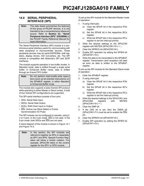
PIC24FJ128GA010 FAMILY14.0 SERIAL PERIPHERALINTERFACE (SPI)Note:The Serial Peripheral Interface (SPI) module is a synchronousserial interface useful for communicating withother peripheral or microcontroller devices. Theseperipheral devices may be serial EEPROMs, shift registers,display drivers, A/D Converters, etc. The SPImodule is compatible with Motorola’s SPI and SIOPinterfaces.The module supports operation in two buffer modes. InStandard mode, data is shifted through a single serialbuffer. In Enhanced Buffer mode, data is shiftedthrough an 8-level FIFO buffer.Note:This data sheet summarizes the featuresof this group of PIC24F devices. It is notintended to be a comprehensive referencesource. Refer to Section 23. “SerialPeripheral Interface (SPI)” (DS39699) inthe PIC24F Family Reference Manual formore information.Do not perform read-modify-write operations(such as bit-oriented instructions) onthe SPIxBUF register, in either Standardor Enhanced Buffer mode.The module also supports a basic framed SPI protocolwhile operating in either Master or Slave modes. A totalof four framed SPI configurations are supported.The SPI serial interface consists of four pins:• SDIx: Serial Data Input• SDOx: Serial Data Output• SCKx: Shift Clock Input or Output• SSx: Active-Low Slave Select or FrameSynchronization I/O PulseThe SPI module can be configured to operate, using 2,3 or 4 pins. In the 3-pin mode, SSx is not used. In the2-pin mode, both SDOx and SSx are not used.A block diagram of the module is shown in Figure 14-1and Figure 14-2.To set up the SPI module for the Standard Master modeof operation:1. If using interrupts:a) Clear the SPIxIF bit in the respective IFSxregister.b) Set the SPIxIE bit in the respective IECxregister.c) Write the SPIxIP bits in the respective IPCxregister to set the interrupt priority.2. Write the desired settings to the SPIxCONregister with MSTEN (SPIxCON1) = 1.3. Clear the SPIROV bit (SPIxSTAT).4. Enable SPI operation by setting the SPIEN bit(SPIxSTAT).5. Write the data to be transmitted to the SPIxBUFregister. Transmission (and reception) will startas soon as data is written to the SPIxBUFregister.To set up the SPI module for the Standard Slave modeof operation:1. Clear the SPIxBUF register.2. If using interrupts:a) Clear the SPIxIF bit in the respective IFSxregister.b) Set the SPIxIE bit in the respective IECxregister.c) Write the SPIxIP bits in the respective IPCxregister to set the interrupt priority.3. Write the desired settings to the SPIxCON1 andSPIxCON2 registers with MSTEN(SPIxCON1) = 0.4. Clear the SMP bit.5. If the CKE bit is set, then the SSEN bit(SPIxCON1) must be set to enable the SSxpin.6. Clear the SPIROV bit (SPIxSTAT).7. Enable SPI operation by setting the SPIEN bit(SPIxSTAT).Note:In this section, the SPI modules arereferred to together as SPIx or separatelyas SPI1 and SPI2. Special Function Registerswill follow a similar notation. Forexample, SPIxCON refers to the controlregister for the SPI1 or SPI2 module.© 2009 <strong>Microchip</strong> Technology Inc. DS39747E-page 121


