pic24fj128ga010 family - Microchip
pic24fj128ga010 family - Microchip
pic24fj128ga010 family - Microchip
You also want an ePaper? Increase the reach of your titles
YUMPU automatically turns print PDFs into web optimized ePapers that Google loves.
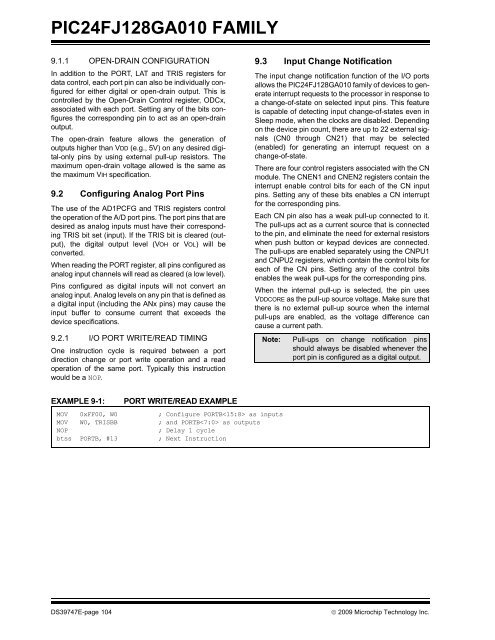
PIC24FJ128GA010 FAMILY9.1.1 OPEN-DRAIN CONFIGURATIONIn addition to the PORT, LAT and TRIS registers fordata control, each port pin can also be individually configuredfor either digital or open-drain output. This iscontrolled by the Open-Drain Control register, ODCx,associated with each port. Setting any of the bits configuresthe corresponding pin to act as an open-drainoutput.The open-drain feature allows the generation ofoutputs higher than VDD (e.g., 5V) on any desired digital-onlypins by using external pull-up resistors. Themaximum open-drain voltage allowed is the same asthe maximum VIH specification.9.2 Configuring Analog Port PinsThe use of the AD1PCFG and TRIS registers controlthe operation of the A/D port pins. The port pins that aredesired as analog inputs must have their correspondingTRIS bit set (input). If the TRIS bit is cleared (output),the digital output level (VOH or VOL) will beconverted.When reading the PORT register, all pins configured asanalog input channels will read as cleared (a low level).Pins configured as digital inputs will not convert ananalog input. Analog levels on any pin that is defined asa digital input (including the ANx pins) may cause theinput buffer to consume current that exceeds thedevice specifications.9.2.1 I/O PORT WRITE/READ TIMINGOne instruction cycle is required between a portdirection change or port write operation and a readoperation of the same port. Typically this instructionwould be a NOP.9.3 Input Change NotificationThe input change notification function of the I/O portsallows the PIC24FJ128GA010 <strong>family</strong> of devices to generateinterrupt requests to the processor in response toa change-of-state on selected input pins. This featureis capable of detecting input change-of-states even inSleep mode, when the clocks are disabled. Dependingon the device pin count, there are up to 22 external signals(CN0 through CN21) that may be selected(enabled) for generating an interrupt request on achange-of-state.There are four control registers associated with the CNmodule. The CNEN1 and CNEN2 registers contain theinterrupt enable control bits for each of the CN inputpins. Setting any of these bits enables a CN interruptfor the corresponding pins.Each CN pin also has a weak pull-up connected to it.The pull-ups act as a current source that is connectedto the pin, and eliminate the need for external resistorswhen push button or keypad devices are connected.The pull-ups are enabled separately using the CNPU1and CNPU2 registers, which contain the control bits foreach of the CN pins. Setting any of the control bitsenables the weak pull-ups for the corresponding pins.When the internal pull-up is selected, the pin usesVDDCORE as the pull-up source voltage. Make sure thatthere is no external pull-up source when the internalpull-ups are enabled, as the voltage difference cancause a current path.Note:Pull-ups on change notification pinsshould always be disabled whenever theport pin is configured as a digital output.EXAMPLE 9-1: PORT WRITE/READ EXAMPLEMOV 0xFF00, W0 ; Configure PORTB as inputsMOV W0, TRISBB ; and PORTB as outputsNOP; Delay 1 cyclebtss PORTB, #13 ; Next InstructionDS39747E-page 104© 2009 <strong>Microchip</strong> Technology Inc.


