MC34152, MC33152, NCV33152 High Speed Dual MOSFET Drivers
MC34152, MC33152, NCV33152 High Speed Dual MOSFET Drivers
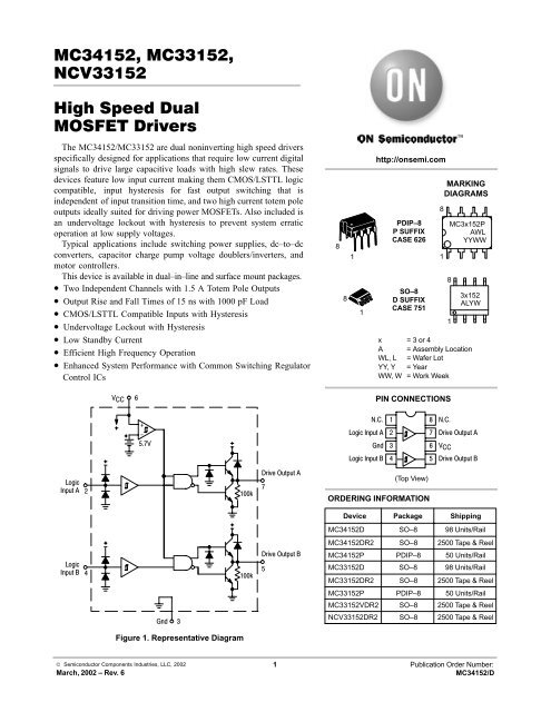
MC34152, MC33152, NCV33152 High Speed Dual MOSFET Drivers

You also want an ePaper? Increase the reach of your titles
YUMPU automatically turns print PDFs into web optimized ePapers that Google loves.
<strong>MC34152</strong>, <strong>MC33152</strong>, <strong>NCV33152</strong>LAYOUT CONSIDERATIONS<strong>High</strong> frequency printed circuit layout techniques areimperative to prevent excessive output ringing andovershoot. Do not attempt to construct the driver circuiton wire–wrap or plug–in prototype boards. Whendriving large capacitive loads, the printed circuit boardmust contain a low inductance ground plane to minimizethe voltage spikes induced by the high ground ripplecurrents. All high current loops should be kept as short aspossible using heavy copper runs to provide a lowimpedance high frequency path. For optimum driveperformance, it is recommended that the initial circuitdesign contains dual power supply bypass capacitorsconnected with short leads as close to the VCC pin andground as the layout will permit. Suggested capacitors area low inductance 0.1 µF ceramic in parallel with a 4.7 µFtantalum. Additional bypass capacitors may be requireddepending upon Drive Output loading and circuit layout.Proper printed circuit board layout is extremelycritical and cannot be over emphasized. Figure 19. Enhanced System Performance withCommon Switching RegulatorsFigure 20. <strong>MOSFET</strong> Parasitic Oscillations Figure 21. Direct Transformer DriveFigure 22. Isolated <strong>MOSFET</strong> Drivehttp://onsemi.com8
<strong>MC34152</strong>, <strong>MC33152</strong>, <strong>NCV33152</strong>Figure 23. Controlled <strong>MOSFET</strong> DriveFigure 24. Bipolar Transistor Drive ≈≈Figure 25. <strong>Dual</strong> Charge Pump ConverterOutput Load RegulationIO (mA) +VO (V) –VO (V)0 27.7 –13.31.0 27.4 –12.910 26.4 –11.920 25.5 –11.230 24.6 –10.550 22.6 –9.4http://onsemi.com9
<strong>MC34152</strong>, <strong>MC33152</strong>, <strong>NCV33152</strong>PACKAGE DIMENSIONSP SUFFIXPLASTIC PACKAGECASE 626–05ISSUE L–B– NOTE 2–T–HF–A–GCND K LJM http://onsemi.com10
<strong>MC34152</strong>, <strong>MC33152</strong>, <strong>NCV33152</strong>PACKAGE DIMENSIONS–X–B–Y––Z–HGADSC D SUFFIXPLASTIC PACKAGECASE 751–07(SO–8)ISSUE WN X 45MKJ http://onsemi.com11
<strong>MC34152</strong>, <strong>MC33152</strong>, <strong>NCV33152</strong>ON Semiconductor and are trademarks of Semiconductor Components Industries, LLC (SCILLC). SCILLC reserves the right to make changeswithout further notice to any products herein. SCILLC makes no warranty, representation or guarantee regarding the suitability of its products for any particularpurpose, nor does SCILLC assume any liability arising out of the application or use of any product or circuit, and specifically disclaims any and all liability,including without limitation special, consequential or incidental damages. “Typical” parameters which may be provided in SCILLC data sheets and/orspecifications can and do vary in different applications and actual performance may vary over time. All operating parameters, including “Typicals” must bevalidated for each customer application by customer’s technical experts. SCILLC does not convey any license under its patent rights nor the rights of others.SCILLC products are not designed, intended, or authorized for use as components in systems intended for surgical implant into the body, or other applicationsintended to support or sustain life, or for any other application in which the failure of the SCILLC product could create a situation where personal injury or deathmay occur. Should Buyer purchase or use SCILLC products for any such unintended or unauthorized application, Buyer shall indemnify and hold SCILLCand its officers, employees, subsidiaries, affiliates, and distributors harmless against all claims, costs, damages, and expenses, and reasonable attorney feesarising out of, directly or indirectly, any claim of personal injury or death associated with such unintended or unauthorized use, even if such claim alleges thatSCILLC was negligent regarding the design or manufacture of the part. SCILLC is an Equal Opportunity/Affirmative Action Employer.PUBLICATION ORDERING INFORMATIONLiterature Fulfillment:Literature Distribution Center for ON SemiconductorP.O. Box 5163, Denver, Colorado 80217 USAPhone: 303–675–2175 or 800–344–3860 Toll Free USA/CanadaFax: 303–675–2176 or 800–344–3867 Toll Free USA/CanadaEmail: ONlit@hibbertco.comN. American Technical Support: 800–282–9855 Toll Free USA/CanadaJAPAN: ON Semiconductor, Japan Customer Focus Center4–32–1 Nishi–Gotanda, Shinagawa–ku, Tokyo, Japan 141–0031Phone: 81–3–5740–2700Email: r14525@onsemi.comON Semiconductor Website: http://onsemi.comFor additional information, please contact your localSales Representative.http://onsemi.com12<strong>MC34152</strong>/D