Create successful ePaper yourself
Turn your PDF publications into a flip-book with our unique Google optimized e-Paper software.
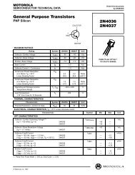
SWITCHING CHARACTERISTICS* (CL = 50 pF, TA = 25 C)ÎÎÎÎÎÎÎÎÎÎÎÎÎÎÎÎÎÎÎÎÎÎÎÎÎÎÎÎÎÎÎÎÎÎÎÎÎÎÎÎÎÎÎÎÎÎÎÎÎÎÎÎÎÎÎÎÎÎÎÎÎÎÎÎÎÎÎÎÎÎÎÎÎÎÎÎÎÎÎÎÎÎÎÎÎÎÎÎÎÎÎÎÎÎÎÎÎÎÎÎÎÎCharacteristic Symbol VDD Min Typ # Max UnitÎÎÎÎÎÎÎÎÎÎÎÎÎÎÎÎÎÎÎÎÎÎÎÎÎÎÎÎÎÎÎÎÎÎOutput Rise and Fall TimenstTLH, tTHL = (1.5 ns/pF) CL + 25 nstTLH, tTHL = (0.75 ns/pF) CL + 12.5 nstTLH, tTHL = (0.55 ns/pF) CL + 9.5 nsData Propagation Delay TimetPLH = (1.7 ns/pF) CL + 210 nstPLH = (0.66 ns/pF) CL + 77 nstPLH = (0.5 ns/pF) CL + 50 nstPHL = (1.7 ns/pF) CL + 185 nstPHL = (0.66 ns/pF) CL + 62 nstPHL = (0.5 ns/pF) CL + 40 nsExpand Propagation Delay TimetPLH = (1.7 ns/pF) CL + 95 nstPLH = (0.66 ns/pF) CL + 42 nstPLH = (0.5 ns/pF) CL + 25 nstPHL = (1.7 ns/pF) CL + 115 nstPHL = (0.66 ns/pF) CL + 47 nstPHL = (0.5 ns/pF) CL + 30 nsInhibit Propagation Delay TimetPLH = (1.7 ns/pF) CL + 135 nstPLH = (0.66 ns/pF) CL + 67 nstPLH = (0.5 ns/pF) CL + 40 nstPHL = (1.7 ns/pF) CL + 145 nstPHL = (0.66 ns/pF) CL + 62 nstPHL = (0.5 ns/pF) CL + 35 ns3–State Propagation Delay Time“1” to High ImpedancetTLH, tTHLtPLH5.010155.01015tPHL 5.01015tPLH5.01015tPHL 5.01015tPLH5.01015tPHL 5.01015tPHZ“0” to High Impedance tPLZ 5.01015High Impedance to “1” tPZH 5.01015High Impedance to “0” tPZL 5.01015* The formulas given are for the typical characteristics only at 25 C.#Data labelled “Typ” Is not to be used for design purposes but is intended as an indication of the IC’s potential performance.5.01015—————————————————————————————————10050402951107527095651807550200805522010065230956060453590554011050401707050200100805802251804801751404301601253301109050022516040017515015011090225140100300125100425175125nsnsnsnsnsnsnsnsnsns1616Vout , OUTPUT VOLTAGE (Vdc)1412108.06.04.02.000abcabc5.0 Vdc2.0 4.06.0a bc10 Vdc8.010Vin, INPUT VOLTAGE (Vdc)(a) Expand InputsVDD = 15 VdcUNUSED INPUTSCONNECTED TOVSSa TA = + 125°Cb TA = + 25°Cc TA = – 55°C121416Vout , OUTPUT VOLTAGE (Vdc)14 VDD = 15 Vdc121010 Vdca8.0 bc6.05.0 Vdc4.0ab2.0c00 2.0 4.06.0abc8.010Vin, INPUT VOLTAGE (Vdc)(b) Data InputsabcTA = + 125°CTA = + 25°CTA = – 55°CA AND B CONNECTED TO VinENABLE INPUT CONNECTED TOVDD. OTHER INPUTS CONNECTEDTO VSS.121416Figure 1. Typical Voltage Transfer CharacteristicsMOTOROLA CMOS LOGIC DATA<strong>MC14506</strong>UB3