Uncooled linear arrays based on LiTaO3 - DIAS Infrared GmbH
Uncooled linear arrays based on LiTaO3 - DIAS Infrared GmbH
Uncooled linear arrays based on LiTaO3 - DIAS Infrared GmbH

You also want an ePaper? Increase the reach of your titles
YUMPU automatically turns print PDFs into web optimized ePapers that Google loves.
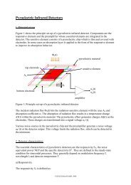
<strong>DIAS</strong> <strong>Infrared</strong> <strong>GmbH</strong> – Publicati<strong>on</strong>s – No. 8 1<str<strong>on</strong>g>Uncooled</str<strong>on</strong>g> <str<strong>on</strong>g>linear</str<strong>on</strong>g> <str<strong>on</strong>g>arrays</str<strong>on</strong>g> <str<strong>on</strong>g>based</str<strong>on</strong>g> <strong>on</strong> LiTaO 3Volkmar Norkus, Gerald Gerlach, Dresden University of Technology, Institute for Solid-State Electr<strong>on</strong>ics,Günter Hofmann, <strong>DIAS</strong> <strong>Infrared</strong> <strong>GmbH</strong>Numerous applicati<strong>on</strong>s in the field of infrared measurement technology demand uncooled <str<strong>on</strong>g>linear</str<strong>on</strong>g> <str<strong>on</strong>g>arrays</str<strong>on</strong>g>which show such qualities as high signal-to-noise ratio, appropriate spatial resoluti<strong>on</strong>, reas<strong>on</strong>ablecosts as well as reproducible detector parameters that are stable in the l<strong>on</strong>g run.This paper gives a survey of both the design and essential properties of recently developed pyroelectric<str<strong>on</strong>g>linear</str<strong>on</strong>g> <str<strong>on</strong>g>arrays</str<strong>on</strong>g> with integrated CMOS multiplexer made <strong>on</strong> the basis of lithium tantalate (LiTaO 3 ).There are up to 256 resp<strong>on</strong>sive elements with a minimum pitch of 50 µm in the <str<strong>on</strong>g>linear</str<strong>on</strong>g> <str<strong>on</strong>g>arrays</str<strong>on</strong>g>. Thanksto the development of a flexible manufacture technology as well as to the further development of subtechnologiesthere has been a permanent improvement of the thermal and spatial detector resoluti<strong>on</strong>capacity. At the same time it has become possible to adapt the detector layout and design to theplanned applicati<strong>on</strong> to a large extent even for a small number of items. The paper dem<strong>on</strong>strates thatreducing the thickness of the resp<strong>on</strong>sive elements and providing good thermal isolati<strong>on</strong> at the sametime is a way to improve the signal-to-noise ratio many times.Some of the applicati<strong>on</strong>s of LiTaO 3 -<str<strong>on</strong>g>linear</str<strong>on</strong>g> <str<strong>on</strong>g>arrays</str<strong>on</strong>g> are infrared line cameras for the n<strong>on</strong>-c<strong>on</strong>tact temperaturemeasurement as well as spectrometers in the wavelength range of 0.8…25 µm.1 Introducti<strong>on</strong>Pyroelectric infrared detectors al<strong>on</strong>g with thermopiles and bolometers bel<strong>on</strong>g to the group of thermaldetectors. The advantage of these detectors is that they can be operated at room temperature, additi<strong>on</strong>allythey show a very homogenous spectral resp<strong>on</strong>sivity in the wavelength range of 0.8…25 µmcompared to semic<strong>on</strong>ductor detectors. The spectral ranges 3…5 µm and 8…14 µm are of particulartechnical importance.Figure 1 shows the principal design of a pyroelectric <str<strong>on</strong>g>linear</str<strong>on</strong>g> array. Its essential comp<strong>on</strong>ents are thepyroelectric chip and the read-out circuit, where each of the individual resp<strong>on</strong>sive elements is c<strong>on</strong>nectedwith an input structure of the circuit. The incident radiati<strong>on</strong> flux Φ S (t) is absorbed by the resp<strong>on</strong>siveelement with the area A S and causes a temperature change ∆T(t) in the pyroelectric material.This results in a change of the sp<strong>on</strong>taneous polarisati<strong>on</strong> in the material (pyroelectric effect), whichcauses charges to build up at the electrodes. These charges are read into the circuit and generate a signalvoltage u′S at the circuit output. Al<strong>on</strong>g with the signal voltage u′S a noise voltage u′R occurs at theoutput. The latter is generated by internal noise sources in the pyroelectric chip as well as in the circuit.It limits the least detectable radiati<strong>on</strong> flux.Some detector parameters can be used to quantitatively describe the performance of <str<strong>on</strong>g>linear</str<strong>on</strong>g> <str<strong>on</strong>g>arrays</str<strong>on</strong>g>[1]. The resp<strong>on</strong>sivity S V describes the dependence of the signal voltage u′ S <strong>on</strong> the incident radiati<strong>on</strong>flux Φ S (t) for the spatial frequency R = 0:SV∆ u′∆ΦS= . (1)SThe noise equivalent power (NEP) is the least detectable change of the radiati<strong>on</strong> flux ∆Φ S , whichgenerates a signal voltage change ∆ u′S at the detector output, which corresp<strong>on</strong>ds to the effective valueof the noise voltage u′R :
<strong>DIAS</strong> <strong>Infrared</strong> <strong>GmbH</strong> – Publicati<strong>on</strong>s – No. 8 2∆Φ u ′ u′= =∆u′SS R RNEP . (2)SVΦ Sacfr<strong>on</strong>t electrodedbA Spyroelectric chipback electrodexyinput structureoutput structuremultiplexeru SzFigure 1: Principal design of a pyroelectric <str<strong>on</strong>g>linear</str<strong>on</strong>g> arrayThe modulati<strong>on</strong> transfer functi<strong>on</strong> MTF describes the spatial resoluti<strong>on</strong> capacity of an array:SV ( R)MTF( R)= . (3)S ( R = 0)VIdeally the MTF is 1 and the product of the individual modulati<strong>on</strong> transfer functi<strong>on</strong>s of the array.Here the thermal MTF is of particular importance. It is caused by the thermal cross-talk between theresp<strong>on</strong>sive elements as a result of thermal c<strong>on</strong>ducti<strong>on</strong> processes in the pyroelectric material. The detectorqualities that can be obtained are mainly determined by the properties of both the pyroelectricmaterial and the electrode system, the geometry of the resp<strong>on</strong>sive elements, the thermal c<strong>on</strong>tact of theresp<strong>on</strong>sive element with the envir<strong>on</strong>ment, the transfer qualities as well as the noise of the read-outcircuit.For the <str<strong>on</strong>g>arrays</str<strong>on</strong>g> described we get the following equati<strong>on</strong> for the resp<strong>on</strong>sivity S V :SVτ α p vc ´ d 2 C fF= (4)PPChwith: τ F transmittance of the optical windowα absorpti<strong>on</strong> coefficient of the resp<strong>on</strong>sive elementp pyroelectric coefficientc P´ volume-specific heat of pyroelectric materialv amplificati<strong>on</strong> factorC integrati<strong>on</strong> capacitychopping frequency.f ChFrom these facts it is clear that a reduced thickness d P of the resp<strong>on</strong>sive elements results in an increaseof the resp<strong>on</strong>sivity.
<strong>DIAS</strong> <strong>Infrared</strong> <strong>GmbH</strong> – Publicati<strong>on</strong>s – No. 8 32 Linear array <str<strong>on</strong>g>based</str<strong>on</strong>g> <strong>on</strong> LiTaO 3The research work d<strong>on</strong>e in the field of pyroelectric detector development and applicable materials atour institute over many years has shown that LiTaO 3 is an excellent and proven material for the manufactureof infrared detectors. It is easy to treat this material mechanically and its chemical resistance isvery good. There are single-crystalline polarised LiTaO 3 wafers <strong>on</strong> the market, which have a diameterof up to 3" and thicknesses of 40…80 µm as a minimum.Table 1 shows measured properties of LiTaO 3 that are detector-specific. Arrays <str<strong>on</strong>g>based</str<strong>on</strong>g> <strong>on</strong> LiTaO 3dem<strong>on</strong>strate excellent l<strong>on</strong>g-term durability and reproducibility of detector qualities as well as a verysmall dependence of the resp<strong>on</strong>sivity up<strong>on</strong> the ambient temperature.p c P ' ε P ' tan δ (1 kHz) a P1,8 x 10 -8 C cm -2 K -1 3,2 J cm -3 K -1 43 5 x 10 -4 1,8 x 10 -2 cm 2 s -1Table 1: Measured properties of LiTaO 3 (T = 25°C)2.1 Pyroelectric chipIn the past years was made an extensive work for the development and optimizati<strong>on</strong> of numeroussubtechnologies for the reproducible and high-yield producti<strong>on</strong> of self-supporting LiTaO 3 chips withup to 256 resp<strong>on</strong>sive elements and a thickness of the resp<strong>on</strong>sive elements smaller than 10 µm [2] [3].The methods comprise mechanical and mechanical-chemical polishing and i<strong>on</strong>-beam etching as well[4]. Figure 2 shows the typical layout of two different chip types.resp<strong>on</strong>siveelementbackelectrodesystemisolati<strong>on</strong> trenchfr<strong>on</strong>telectrodesystempyroelectric chipback electrodegroove20a) b)dpFigure 2: Chip layout with typical dimensi<strong>on</strong>s (µm)a) standard chip (<strong>on</strong>ly mechanical polishing)b) i<strong>on</strong>-beam-etched chipAfter the fr<strong>on</strong>t electrode systems have been structured the LiTaO 3 wafers of about 500 µm thicknessare thinned to a thickness of about 30 µm by mechanical lapping and polishing processes. After thatthe wafers are mechanically and chemically polished to a final thickness of about 20 µm. The chipsurface is of optical quality. The chips dem<strong>on</strong>strate a typical plane parallelism that is better than± 1 µm. For the manufacture of standard chips the back electrode system is photolithographicallystructured after the treatment. After the chips have been detached from the machining carrier theyshow the dimensi<strong>on</strong>s [14,500 -100 x 1,600 -100 x 20 ±0 ] µm 3 and are ready for further packaging processes.
<strong>DIAS</strong> <strong>Infrared</strong> <strong>GmbH</strong> – Publicati<strong>on</strong>s – No. 8 4To produce chips with even thinner resp<strong>on</strong>sive elements i<strong>on</strong>-beam etching (IBE) is carried out afterpolishing. I<strong>on</strong>-beam etching is a dry-etching technique, whose process parameter may excellently beadjusted to the specific structuring task. While the back electrode trench is being etched (see figure 2),the chip edge area is covered by a photoresist mask. The thicker chip edge area provides the mechanicalstability necessary after etching for the handling of the self-supporting chips, in particular forpackaging and b<strong>on</strong>ding. For the process parameters applied typical etching rates for LiTaO 3 are40…100 nm/min. Using the i<strong>on</strong>-beam etching technique <str<strong>on</strong>g>linear</str<strong>on</strong>g> <str<strong>on</strong>g>arrays</str<strong>on</strong>g> with a resp<strong>on</strong>sive elementthickness of less than 2 µm were produced. The feasible minimum thickness of the pyroelectric materialin the trench area is primarily determined by the obtained plane parallelism of the polished chipsas well as by the user request for the resp<strong>on</strong>sivity homogeneity over all resp<strong>on</strong>sive elements. For thereducti<strong>on</strong> of the thermal cross-talk between the resp<strong>on</strong>sive elements and – as a result – for the MTFimprovement thermal isolati<strong>on</strong> trenches can be etched between the resp<strong>on</strong>sive elements. Typicaltrench widths are 5…10 µm for a length of 300 µm [5].2.2 Packaging & housingThe packaging & housing of the individual detector comp<strong>on</strong>ents is of decisive importance for themanufacture of l<strong>on</strong>g-term durable and reliable infrared detectors. The <str<strong>on</strong>g>linear</str<strong>on</strong>g> <str<strong>on</strong>g>arrays</str<strong>on</strong>g> with chip lengths upto 14,500 µm are placed in a 16-pole hermetic metal housing with the dimensi<strong>on</strong>s [22 x 32 x 3.5] mm 3 . Ahybrid arrangement is applied for the <str<strong>on</strong>g>linear</str<strong>on</strong>g> <str<strong>on</strong>g>arrays</str<strong>on</strong>g>. The read-out circuit and a subcarrier with the pyroelectricchip are placed <strong>on</strong> a thick-layer wiring carrier. The chip's resp<strong>on</strong>sive elements are arrangedin the centre of the housing. The individual elements <strong>on</strong> the chip are electrically b<strong>on</strong>ded with the b<strong>on</strong>dpads of the read-out circuits by ultras<strong>on</strong>ic wire b<strong>on</strong>ding. At the time being the minimum b<strong>on</strong>d pitch is50 µm. At present we use a CMOS-analogue switch structure with C/V c<strong>on</strong>verter and with low-noisepreamplifiers, which has been especially developed for the read-out circuit.Moreover, a temperature detector is integrated in the housing. The infrared-transmissive window ischosen in dependence of the array applicati<strong>on</strong>. Applicati<strong>on</strong>s of very broad bands call for calcium fluoride(0.1…9 µm), KRS-5 (0.65…30 µm) and sapphire (0.4…5 µm) for example. For wave lengths of3…5 µm and 8…12 µm bandpass filters are used.1.0E+07Resp<strong>on</strong>sivity [V/W]1.0E+061.0E+050 5 10 15 20Thickness [µm]Figure 3: Measured dependence of resp<strong>on</strong>sivity S V <strong>on</strong> the thickness d P ofthe resp<strong>on</strong>sive elements compared to the calculated values2.3 Array propertiesFigure 3 shows a comparis<strong>on</strong> between the measured dependence of the resp<strong>on</strong>sivity <strong>on</strong> the resp<strong>on</strong>siveelement thickness and the calculated values. The <str<strong>on</strong>g>arrays</str<strong>on</strong>g> c<strong>on</strong>tain 128 resp<strong>on</strong>sive elements with a pitch of100 µm. The resp<strong>on</strong>sive surface covers an area of [90 x 100] µm 2 . The measurements were carried outwith a germanium window bloomed for 8…14 µm. The mean absorpti<strong>on</strong> coefficient α of the resp<strong>on</strong>sive
<strong>DIAS</strong> <strong>Infrared</strong> <strong>GmbH</strong> – Publicati<strong>on</strong>s – No. 8 5element amounted to 0.61. The measurements were performed at ambient temperature (T = 25 °C) usingrectangular chopping at 128 Hz. Deviati<strong>on</strong>s result from the measuring errors in the determinati<strong>on</strong> of thethickness of the resp<strong>on</strong>sive elements and the reducti<strong>on</strong> of the overall absorpti<strong>on</strong> coefficient of the radiati<strong>on</strong>-sensitiveelements due to the reduced self-absorpti<strong>on</strong> of LiTaO 3 [α <strong>LiTaO3</strong> = f(d p )].Number of Elements Pitch c [µm] Size of Element a x b [µm 2 ]1 x 128 100 90 x 1001 x 128 100 90 x 5001 x 128 100 90 x 10001 x 128 100 90 x 15001 x 128 100 90 x 23001 x 256 100 90 x 1001 x 256 50 40 x 50Table 2: Typical c<strong>on</strong>figurati<strong>on</strong>s of <str<strong>on</strong>g>linear</str<strong>on</strong>g> <str<strong>on</strong>g>arrays</str<strong>on</strong>g>Number of Elements 1 x 128 1 x 128 1 x 128 1 x 256Size of Elements [µm 2 ] 90 x 100 90 x 100 90 x 2300 40 x 50Pitch [µm] 100 100 100 50Element Thickness [µm] 20 5 20 5Resp<strong>on</strong>sivity S V [VW -1 ] 200 000 500 000 200 000 500 000Variati<strong>on</strong> S V 1…2 % 2…5 % 1…2 % 3…6 %NEP [nW] 5 (2.5) 2 (1) 6 (3) 2 (1)NETD (300 K, F/1-optic) [K] 0.8 (0.4) 0.3 (0.15) 0.04 (0.02) 1.4 (0.7)MTF (R = 3 lp/mm) 0.6 0.6 0.6 0.7( )-values: additi<strong>on</strong>al 4 accumulati<strong>on</strong>s (frame rate 32 Hz)Table 3: Typical properties of <str<strong>on</strong>g>linear</str<strong>on</strong>g> <str<strong>on</strong>g>arrays</str<strong>on</strong>g>(rectangular chopping with 128 Hz, array temperature 25 °C, Ge*)MTF10.80.60.410 Hz40 Hz128 Hzgeometric0.200 1 2 3 4 5R [lp/mm]Figure 4: Frequency dependence of the MTF for a <str<strong>on</strong>g>linear</str<strong>on</strong>g> array without isolati<strong>on</strong> trenchesTable 2 shows a survey of <str<strong>on</strong>g>linear</str<strong>on</strong>g> <str<strong>on</strong>g>arrays</str<strong>on</strong>g> built so far and their element geometry. A special packagingand structuring technique facilitates the manufacture of very l<strong>on</strong>g <str<strong>on</strong>g>linear</str<strong>on</strong>g> <str<strong>on</strong>g>arrays</str<strong>on</strong>g> with more than 256 elementsin the pitch ≥ 50 µm. Table 3 shows essential properties of different detector types. Figure 4 showsthe frequency dependence of the MTF for a 128-element <str<strong>on</strong>g>linear</str<strong>on</strong>g> array without thermal isolati<strong>on</strong> trenches.It clearly shows that the MTF of the <str<strong>on</strong>g>linear</str<strong>on</strong>g> array improves with the chopping frequency increasing, sincethe thermal diffusi<strong>on</strong> length of the temperature wave in the pyroelectric material decreases. What is importantfor the user is that by an increased chopping frequency within certain limits the spatial detectorresoluti<strong>on</strong> can be improved at the expense of the thermal resoluti<strong>on</strong> (with the resp<strong>on</strong>sivity decreasing).
<strong>DIAS</strong> <strong>Infrared</strong> <strong>GmbH</strong> – Publicati<strong>on</strong>s – No. 8 6The etching of thermal isolati<strong>on</strong> trenches brought about an enormous improvement of the MTF of <str<strong>on</strong>g>arrays</str<strong>on</strong>g>with 256 elements [5].L<strong>on</strong>g-term investigati<strong>on</strong>s that had been carried through over up to five years showed that there wereno changes of the array parameters within the accuracy limits of the measuring set-ups.3 Array applicati<strong>on</strong>sVarious types of the <str<strong>on</strong>g>linear</str<strong>on</strong>g> <str<strong>on</strong>g>arrays</str<strong>on</strong>g> presented are applied in infrared systems for n<strong>on</strong>-c<strong>on</strong>tact temperaturemeasurement. These are <strong>on</strong> the <strong>on</strong>e hand line cameras such as the PYROLINE system madeby the <strong>DIAS</strong> Angewandte Sensorik <strong>GmbH</strong> [6] and <strong>on</strong> the other hand scanning systems, too [7]. Togetherwith dispersing optical elements (prisms, gratings) the <str<strong>on</strong>g>arrays</str<strong>on</strong>g> are applied in infrared spectrometers[8]. At present investigati<strong>on</strong>s are carried out to test their applicati<strong>on</strong> in systems for the fillinglevel measurement in optically n<strong>on</strong>-transparent vessels. For a quick and efficient array operati<strong>on</strong> bythe user a special sensor module has been developed, which comprises the chopper, a low-noise signalprocessing with digitalisati<strong>on</strong>, a computer interface as well as the required clock and power source.4 C<strong>on</strong>clusi<strong>on</strong>sThe manufacture of pyroelectric <str<strong>on</strong>g>linear</str<strong>on</strong>g> <str<strong>on</strong>g>arrays</str<strong>on</strong>g> <str<strong>on</strong>g>based</str<strong>on</strong>g> <strong>on</strong> LiTaO 3 with thicknesses of the selfsupportingresp<strong>on</strong>sive elements of less than 5 µm has become possible by the development of specialthinning techniques (i<strong>on</strong>-beam etching). It has been dem<strong>on</strong>strated that as a result the signal-to-noiseratio can be improved many times in corresp<strong>on</strong>dence with simulati<strong>on</strong> calculati<strong>on</strong>s. The minimumvalue of the NEP achieved so far for a detector with resp<strong>on</strong>sive elements of the dimensi<strong>on</strong>s[90 x 100] µm 2 was 0.2 nW for a chopping frequency of 40 Hz. Since the read-out circuit presentlydetermines the detector noise, there will be a further reducti<strong>on</strong> of the NEP by a new noise-optimizeddesign in the next future.These newly developed <str<strong>on</strong>g>linear</str<strong>on</strong>g> <str<strong>on</strong>g>arrays</str<strong>on</strong>g> <str<strong>on</strong>g>based</str<strong>on</strong>g> <strong>on</strong> LiTaO 3 are rugged and l<strong>on</strong>g-term durable comp<strong>on</strong>entswith both thermal and spatial resoluti<strong>on</strong>, which makes them a good choice for the efficient applicati<strong>on</strong>in systems for n<strong>on</strong>-c<strong>on</strong>tact temperature measurement and process m<strong>on</strong>itoring as well as inspectrometers and security systems at reas<strong>on</strong>able costs.5 AcknowledgementsThis research was supported by the Bundesministerium für Bildung und Forschung, P-Nr. 16SV590.The authors thank Mr. Regenstein for his work in the field of packaging & housing and Mr. Kostka forthe special sample preparati<strong>on</strong>s with i<strong>on</strong> beam etching.6 References[1] G. Hofmann, V. Norkus, H. Budzier, N. Neumann, J. Vollheim, N. Heß, U. Hoffmann, Th. Reichhardt,V. Krause: “<str<strong>on</strong>g>Uncooled</str<strong>on</strong>g> pyroelectric <str<strong>on</strong>g>arrays</str<strong>on</strong>g> for c<strong>on</strong>tactless temperature measurements”, SPIESmart Focal Plane Arrays and Focal Plane Array Testing, Vol. 2474, 1995, pp. 98-109[2] V. Norkus, T. Sokoll, G. Gerlach, G. Hofmann: “Pyroelectric infrared <str<strong>on</strong>g>arrays</str<strong>on</strong>g> and their applicati<strong>on</strong>s”,SPIE <strong>Infrared</strong> Spaceborne Remote Sensing V, Vol. 3122, 1997, pp. 409-419[3] V. Norkus, G. Gerlach, G. Hofmann: “High-resoluti<strong>on</strong> infrared detectors <str<strong>on</strong>g>based</str<strong>on</strong>g> <strong>on</strong> LiTaO 3 ”,Proc. of the 3 rd OPTO C<strong>on</strong>ference, 18.-20. May 1998, Erfurt, pp. 23-28[4] T. Sokoll, V. Norkus, G. Gerlach: “I<strong>on</strong> beam etching of lithium tantalate and its applicati<strong>on</strong> forpyroelectric <str<strong>on</strong>g>linear</str<strong>on</strong>g> <str<strong>on</strong>g>arrays</str<strong>on</strong>g>”, Surface and Coating Technology 97 (1997), pp. 469-474[5] T. Sokoll, V. Norkus, G. Gerlach: “Infrarot-Zeilensensoren mit 256 empfindlichen Elementen aufder Basis v<strong>on</strong> Lithiumtantalat”, Technisches Messen 66 (1999) 3[6] Product informati<strong>on</strong>, “PYROLINE” from <strong>DIAS</strong> Angewandte Sensorik <strong>GmbH</strong>, 1998
<strong>DIAS</strong> <strong>Infrared</strong> <strong>GmbH</strong> – Publicati<strong>on</strong>s – No. 8 7[7] P. Scepko, J. Pancik, S. Havlik: “Development of a Thermal Imaging System for Robotic Visi<strong>on</strong>”,5 th C<strong>on</strong>ference “<strong>Infrared</strong> Sensors and Systems”, Dresden, 8.-9. September 1997, Dresdner Beiträgezur Sensorik, Vol. 4, pp. 89-94[8] F. Nagel, M. Zimmerhackl: “Spectrometer assembly with a pyroelectric array”, 5 th C<strong>on</strong>ference“<strong>Infrared</strong> Sensors and Systems”, Dresden, 8.-9. September 1997, Dresdner Beiträge zur Sensorik,Vol. 4, pp. 113-117