

SG3526 Pulse Width Modulation Control Circuit
SG3526 Pulse Width Modulation Control Circuit
SG3526 Pulse Width Modulation Control Circuit

You also want an ePaper? Increase the reach of your titles
YUMPU automatically turns print PDFs into web optimized ePapers that Google loves.
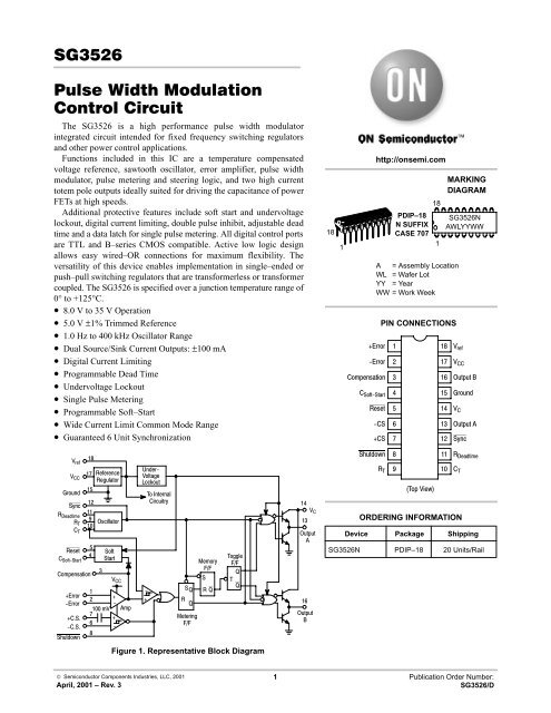
The <strong>SG3526</strong> is a high performance pulse width modulatorintegrated circuit intended for fixed frequency switching regulatorsand other power control applications.Functions included in this IC are a temperature compensatedvoltage reference, sawtooth oscillator, error amplifier, pulse widthmodulator, pulse metering and steering logic, and two high currenttotem pole outputs ideally suited for driving the capacitance of powerFETs at high speeds.Additional protective features include soft start and undervoltagelockout, digital current limiting, double pulse inhibit, adjustable deadtime and a data latch for single pulse metering. All digital control portsare TTL and B–series CMOS compatible. Active low logic designallows easy wired–OR connections for maximum flexibility. Theversatility of this device enables implementation in single–ended orpush–pull switching regulators that are transformerless or transformercoupled. The <strong>SG3526</strong> is specified over a junction temperature range of0° to +125°C.• 8.0 V to 35 V Operation• 5.0 V ±1% Trimmed Reference• 1.0 Hz to 400 kHz Oscillator Range• Dual Source/Sink Current Outputs: ±100 mA• Digital Current Limiting• Programmable Dead Time• Undervoltage Lockout• Single <strong>Pulse</strong> Metering• Programmable Soft–Start• Wide Current Limit Common Mode Range• Guaranteed 6 Unit Synchronization181http://onsemi.comA = Assembly LocationWL = Wafer LotYY = YearWW = Work Week PDIP–18N SUFFIXCASE 707181PIN CONNECTIONSMARKINGDIAGRAM<strong>SG3526</strong>NAWLYYWW Figure 1. Representative Block Diagram ORDERING INFORMATIONDevice Package Shipping<strong>SG3526</strong>N PDIP–18 20 Units/Rail© Semiconductor Components Industries, LLC, 2001April, 2001 – Rev. 31 Publication Order Number:<strong>SG3526</strong>/D
<strong>SG3526</strong>MAXIMUM RATINGS (Note 1.)Rating Symbol Value UnitSupply Voltage V CC +40 VdcCollector Supply Voltage V C +40 VdcLogic Inputs –0.3 to +5.5 VAnalog Inputs –0.3 to V CC VOutput Current, Source or Sink I O ±200 mAReference Load Current (V CC = 40 V, Note 2.) I ref 50 mALogic Sink Current 15 mAPower DissipationT A = +25°C (Note 3.)T C = +25°C (Note 4.)P D10003000Thermal Resistance Junction–to–Air R θJA 100 °C/WThermal Resistance Junction–to–Case R θJC 42 °C/WOperating Junction Temperature T J +150 °CStorage Temperature Range T stg –65 to +150 °CLead Temperature (Soldering, 10 Seconds) T Solder ±300 °CRECOMMENDED OPERATING CONDITIONSCharacteristics Symbol Min Max UnitSupply Voltage V CC 8.0 35 VdcCollector Supply Voltage V C 4.5 35 VdcOutput Sink/Source Current (Each Output) I O 0 ±100 mAReference Load Current I ref 0 20 mAOscillator Frequency Range f osc 0.001 400 kHzOscillator Timing Resistor R T 2.0 150 kΩOscillator Timing Capacitor C T 0.001 20 µFAvailable Deadtime Range (40 kHz) – 3.0 50 %Operating Junction Temperature Range T J 0 +125 °C1. Values beyond which damage may occur.2. Maximum junction temperature must be observed.3. Derate at 10 mW/°C for ambient temperatures above +50°C.4. Derate at 24 mW/°C for case temperatures above +25°C.mWhttp://onsemi.com2
<strong>SG3526</strong>ELECTRICAL CHARACTERISTICS (V CC = +15 Vdc, T J = T low to T high [Note 6.], unless otherwise noted.)Characteristics Symbol Min Typ Max UnitREFERENCE SECTION (Note 7.)Reference Output Voltage (T J = +25°C) V ref 4.90 5.00 5.10 VLine Regulation (+8.0 V ≤ V CC ≤ +35 V) Reg line – 10 30 mVLoad Regulation (0 mA ≤ I L ≤ 20 mA) Reg load – 10 50 mVTemperature Stability ∆V ref /∆T – 10 – mVTotal Reference Output Voltage Variation(+8.0 V ≤ V CC ≤ +35 V, 0 mA ≤ I L ≤ 20 mA)∆V ref 4.85 5.00 5.15 VShort <strong>Circuit</strong> Current (V ref = 0 V) (Note 5.) I SC 25 80 125 mAUNDERVOLTAGE LOCKOUTReset Output Voltage (V ref = +3.8 V) – 0.2 0.4 VReset Output Voltage (V ref = +4.8 V) 2.4 4.8 – VOSCILLATOR SECTION (Note 8.)Initial Accuracy (T J = +25°C) – ±3.0 ±8.0 %Frequency Stability over Power Supply Range(+8.0 V ≤ V CC ≤ +35 V)∆f osc – 0.5 1.0 %∆ VCCFrequency Stability over Temperature(∆T J = T low to T high )Minimum Frequency(R T = 150 kΩ, C T = 20 µF)Maximum Frequency(R T = 2.0 kΩ, C T = 0.001 µF)∆f osc – 2.0 – %∆ T Jf min – 0.5 – Hzf max 400 – – kHzSawtooth Peak Voltage (V CC = +35 V) V osc (P) – 3.0 3.5 VSawtooth Valley Voltage (V CC = +8.0 V) V osc (V) 0.45 0.8 – VERROR AMPLIFIER SECTION (Note 9.)Input Offset Voltage (R S ≤ 2.0 kΩ) V IO – 2.0 10 mVInput Bias Current I IB – –350 –2000 nAInput Offset Current I IO – 35 200 nADC Open Loop Gain (R L ≥ 10 MΩ) A VOL 60 72 – dBHigh Output Voltage(V Pin 1 –V Pin 2 ≥ +150 mV, I source = 100 µA)V OH 3.6 4.2 – VLow Output Voltage(V Pin 2 –V Pin 1 ≥ +150 mV, I sink = 100 µA)V OL – 0.2 0.4 VCommon Mode Rejection Ratio (R S ≤ 2.0 kΩ) CMRR 70 94 – dBPower Supply Rejection Ratio (+12 V ≤ V CC ≤ +18 V) PSRR 66 80 – dB5. Maximum junction temperature must be observed.6. T low = 0°C T high = +125°C7. I L = 0 mA unless otherwise noted.8. f osc = 40 kHz (R T = 4.12 kΩ ± 1%, C T = 0.01 µF ± 1%, R D = 0 Ω)9. 0 V ≤ V CM ≤ +5.2 V.http://onsemi.com3
<strong>SG3526</strong>ELECTRICAL CHARACTERISTICS (continued)Characteristics Symbol Min Typ Max UnitPWM COMPARATOR SECTION (Note 10.)Minimum Duty Cycle(V Compensation = +0.4 V)Maximum Duty Cycle(V Compensation = +3.6 V)DC min – – 0 %DC max 45 49 – %DIGITAL PORTS (SYNC, SHUTDOWN, RESET)Output Voltage(High Logic Level) (I source = 40 µA)(Low Logic Level) (I sink = 3.6 mA)V OH 2.4V OL –4.00.2–0.4VInput Current ⎯ High Logic Level(High Logic Level) (V IH = +2.4 V)(Low Logic Level) (V IL = +0.4 V)I IH –I IL ––125–225–200–360µACURRENT LIMIT COMPARATOR SECTION (Note 12.)Sense Voltage (R S ≤ 50 Ω) V sense 80 100 120 mVInput Bias Current I IB – –3.0 –10 µASOFT–START SECTIONError Clamp Voltage (Reset = +0.4 V) – 0.1 0.4 VC Soft–Start Charging Current (Reset = +2.4 V) I CS 50 100 150 µAOUTPUT DRIVERS (Each Output, V C = +15 Vdc, unless otherwise noted.)Output High LevelI source = 20 mAI source = 100 mAOutput Low LevelI sink = 20 mAI sink = 100 mAV OH12.512V OL––Collector Leakage, V C = +40 V I C(leak) – 50 150 µARise Time (C L = 1000 pF) t r – 0.3 0.6 µsFall Time (C L = 1000 pF) t f – 0.1 0.2 µsSupply Current(Shutdown = +0.4 V, V CC = +35 V, R T = 4.12 kΩ)10. f osc = 40 kHz (R T = 4.12 kΩ ± 1%, C T = 0.01 µF ± 1%, R D = 0 Ω)11. 0 V ≤ V CM ≤ +5.2 V12. 0 V ≤ V CM ≤ +12 V13.5130.21.2––0.32.0I CC – 18 30 mAVVhttp://onsemi.com4
<strong>SG3526</strong> Ω Ω Figure 8. V C Saturation Voltage as aFunction of Sink CurrentFigure 9. Oscillator Period µ µµµµµµ µFigure 10. Error AmplifierFigure 11. Undervoltage LockoutFigure 12. <strong>Pulse</strong> Processing Logichttp://onsemi.com6
<strong>SG3526</strong>APPLICATIONS INFORMATION µ Figure 13. Extending ReferenceOutput Current CapabilityFigure 14. Error Amplifier Connections Figure 15. Oscillator ConnectionsFigure 16. Foldback Current Limiting µ Figure 17. Soft–Start <strong>Circuit</strong>yFigure 18. Driving VMOS Power FETshttp://onsemi.com7
<strong>SG3526</strong> Figure 19. Half–Bridge ConfigurationFigure 20. Flyback Converter withCurrent Limiting Figure 21. Single–Ended ConfigurationFigure 22. Push–Pull Configurationhttp://onsemi.com8
<strong>SG3526</strong>PACKAGE DIMENSIONSPDIP–18N SUFFIXCASE 707–02ISSUE DBLJ HFGADNCKM http://onsemi.com9
<strong>SG3526</strong>Noteshttp://onsemi.com10
<strong>SG3526</strong>Noteshttp://onsemi.com11
<strong>SG3526</strong>ON Semiconductor and are trademarks of Semiconductor Components Industries, LLC (SCILLC). SCILLC reserves the right to make changeswithout further notice to any products herein. SCILLC makes no warranty, representation or guarantee regarding the suitability of its products for any particularpurpose, nor does SCILLC assume any liability arising out of the application or use of any product or circuit, and specifically disclaims any and all liability,including without limitation special, consequential or incidental damages. “Typical” parameters which may be provided in SCILLC data sheets and/orspecifications can and do vary in different applications and actual performance may vary over time. All operating parameters, including “Typicals” must bevalidated for each customer application by customer’s technical experts. SCILLC does not convey any license under its patent rights nor the rights of others.SCILLC products are not designed, intended, or authorized for use as components in systems intended for surgical implant into the body, or other applicationsintended to support or sustain life, or for any other application in which the failure of the SCILLC product could create a situation where personal injury ordeath may occur. Should Buyer purchase or use SCILLC products for any such unintended or unauthorized application, Buyer shall indemnify and holdSCILLC and its officers, employees, subsidiaries, affiliates, and distributors harmless against all claims, costs, damages, and expenses, and reasonableattorney fees arising out of, directly or indirectly, any claim of personal injury or death associated with such unintended or unauthorized use, even if such claimalleges that SCILLC was negligent regarding the design or manufacture of the part. SCILLC is an Equal Opportunity/Affirmative Action Employer.PUBLICATION ORDERING INFORMATIONNORTH AMERICA Literature Fulfillment:Literature Distribution Center for ON SemiconductorP.O. Box 5163, Denver, Colorado 80217 USAPhone: 303–675–2175 or 800–344–3860 Toll Free USA/CanadaFax: 303–675–2176 or 800–344–3867 Toll Free USA/CanadaEmail: ONlit@hibbertco.comFax Response Line: 303–675–2167 or 800–344–3810 Toll Free USA/CanadaN. American Technical Support: 800–282–9855 Toll Free USA/CanadaEUROPE: LDC for ON Semiconductor – European SupportGerman Phone: (+1) 303–308–7140 (Mon–Fri 2:30pm to 7:00pm CET)Email: ONlit–german@hibbertco.comFrench Phone: (+1) 303–308–7141 (Mon–Fri 2:00pm to 7:00pm CET)Email: ONlit–french@hibbertco.comEnglish Phone: (+1) 303–308–7142 (Mon–Fri 12:00pm to 5:00pm GMT)Email: ONlit@hibbertco.comEUROPEAN TOLL–FREE ACCESS*: 00–800–4422–3781*Available from Germany, France, Italy, UK, IrelandCENTRAL/SOUTH AMERICA:Spanish Phone: 303–308–7143 (Mon–Fri 8:00am to 5:00pm MST)Email: ONlit–spanish@hibbertco.comToll–Free from Mexico: Dial 01–800–288–2872 for Access –then Dial 866–297–9322ASIA/PACIFIC: LDC for ON Semiconductor – Asia SupportPhone: 1–303–675–2121 (Tue–Fri 9:00am to 1:00pm, Hong Kong Time)Toll Free from Hong Kong & Singapore:001–800–4422–3781Email: ONlit–asia@hibbertco.comJAPAN: ON Semiconductor, Japan Customer Focus Center4–32–1 Nishi–Gotanda, Shinagawa–ku, Tokyo, Japan 141–0031Phone: 81–3–5740–2700Email: r14525@onsemi.comON Semiconductor Website: http://onsemi.comFor additional information, please contact your localSales Representative.http://onsemi.com12<strong>SG3526</strong>/D


