laser diodes based on gallium nitride - investigation of carrier
laser diodes based on gallium nitride - investigation of carrier
laser diodes based on gallium nitride - investigation of carrier
- No tags were found...

You also want an ePaper? Increase the reach of your titles
YUMPU automatically turns print PDFs into web optimized ePapers that Google loves.
Institute <strong>of</strong> PhysicsPolish Academy <strong>of</strong> SciencesTomasz ŚwietlikLASER DIODES BASED ON GALLIUM NITRIDE -INVESTIGATION OF CARRIER INJECTION MECHANISMS,GAIN AND DISTRIBUTION OFTHE ELECTROMAGNETIC FIELDPH.D. DISSERTATION WRITTEN UNDER THE SUPERVISION OFdoc. dr hab. PIOTR PERLINATINSTITUTE OF HIGH PRESSURE PHYSICSPOLISH ACADEMY OF SCIENCESWarsaw 2008
Table <strong>of</strong> C<strong>on</strong>tentsTable <strong>of</strong> C<strong>on</strong>tentsAcknowledgementsiiiviiSubject and the major goals <strong>of</strong> the dissertati<strong>on</strong> 11 Introducti<strong>on</strong> 51.1 Laser <str<strong>on</strong>g>diodes</str<strong>on</strong>g> and their applicati<strong>on</strong>s . . . . . . . . . . . . . . . . . . . . . . . 51.2 Milest<strong>on</strong>es in early <strong>nitride</strong> research . . . . . . . . . . . . . . . . . . . . . . . 62 Principles <strong>of</strong> a semic<strong>on</strong>ductor <str<strong>on</strong>g>laser</str<strong>on</strong>g> diode operati<strong>on</strong> 92.1 Carrier and phot<strong>on</strong> c<strong>on</strong>finement . . . . . . . . . . . . . . . . . . . . . . . . . 92.2 Carrier injecti<strong>on</strong> and recombinati<strong>on</strong> . . . . . . . . . . . . . . . . . . . . . . 112.3 Basic radiative transiti<strong>on</strong>s . . . . . . . . . . . . . . . . . . . . . . . . . . . . 122.3.1 Sp<strong>on</strong>taneous Emissi<strong>on</strong> . . . . . . . . . . . . . . . . . . . . . . . . . . 122.3.2 Stimulated Emissi<strong>on</strong> . . . . . . . . . . . . . . . . . . . . . . . . . . . 142.4 Material gain . . . . . . . . . . . . . . . . . . . . . . . . . . . . . . . . . . . 152.5 Radiative recombinati<strong>on</strong> mechanisms in <strong>nitride</strong>s . . . . . . . . . . . . . . . . 162.6 Optical modes <strong>of</strong> a res<strong>on</strong>ant cavity . . . . . . . . . . . . . . . . . . . . . . . 182.7 Threshold for lasing acti<strong>on</strong> . . . . . . . . . . . . . . . . . . . . . . . . . . . 202.8 Laser characteristics above threshold . . . . . . . . . . . . . . . . . . . . . . 212.9 Near-field and far-field patterns . . . . . . . . . . . . . . . . . . . . . . . . . 233 Challenges <strong>of</strong> the <strong>nitride</strong>-<str<strong>on</strong>g>based</str<strong>on</strong>g> <str<strong>on</strong>g>laser</str<strong>on</strong>g> technology 253.1 Crystal quality . . . . . . . . . . . . . . . . . . . . . . . . . . . . . . . . . . 253.2 Operating voltage and charge transport . . . . . . . . . . . . . . . . . . . . 263.3 Sp<strong>on</strong>taneous and piezoelectric polarizati<strong>on</strong> . . . . . . . . . . . . . . . . . . . 273.4 Thermal properties . . . . . . . . . . . . . . . . . . . . . . . . . . . . . . . . 303.5 Guiding <strong>of</strong> the optical mode . . . . . . . . . . . . . . . . . . . . . . . . . . . 30iii
9 Optimizati<strong>on</strong> <strong>of</strong> a <str<strong>on</strong>g>laser</str<strong>on</strong>g> cavity design 1159.1 Determinati<strong>on</strong> and significance <strong>of</strong> the unamplified sp<strong>on</strong>taneous emissi<strong>on</strong> spectra1159.2 Optimizati<strong>on</strong> <strong>of</strong> a res<strong>on</strong>ant cavity length . . . . . . . . . . . . . . . . . . . . 1209.3 Optimum quantum well number . . . . . . . . . . . . . . . . . . . . . . . . . 127C<strong>on</strong>clusi<strong>on</strong>s 129A 131Bibliography 135v
AcknowledgementsI am grateful to every<strong>on</strong>e whose involvement c<strong>on</strong>tributed to the successful completi<strong>on</strong> <strong>of</strong>this work.In particular, I would like to thank doc. dr hab. Piotr Perlin, my supervisor, for his manysuggesti<strong>on</strong>s and c<strong>on</strong>stant support during this research. I am also thankful to pr<strong>of</strong>. TadeuszSuski for his guidance through all years <strong>of</strong> my scientific work.I would also like to thank the following:– Gijs Franssen and Szym<strong>on</strong> Grzanka for countless discussi<strong>on</strong>s and useful remarks– Przemek Wi`sniewski and Alexander Khachapuridze for help and instructi<strong>on</strong>s duringmy experimental work– Henryk Teisseyre for a productive cooperati<strong>on</strong> in optical laboratory– Robert Czernecki, Grzegorz Targowski, Micha̷l Leszczyǹski, Pawe̷l Prystawko, Czes̷lawSkierbiszewski, Marcin Siekacz, Ania Feduniewicz-Żmuda for providing samples investigatedin this work– Kasia Komorowska, ̷Lucja Mar<strong>on</strong>a, Jurek Plesiewicz for a nice atmosphere and cooperati<strong>on</strong>– Ulrich Schwarz for <strong>of</strong>fering the opportunity to visit Regensburg University and performSNOM measurements– pr<strong>of</strong>. Saulius Juršėnas and Saulius Miasojedovas for a warm welcome at VilniusUniversity and support in time-resolved spectral analysis– Di<strong>on</strong>yz Pogany and Sergey Bychikhin for performing scans using TIM technique atthe University <strong>of</strong> Vienna– Tomasz Ochalski from University College Cork for help in collecti<strong>on</strong> high resoluti<strong>on</strong>electroluminescence spectra <strong>of</strong> <str<strong>on</strong>g>laser</str<strong>on</strong>g> devicesvii
viii– Irena Makarowa, Wiktor Krupczyǹski, Renata Wi`sniewska for the sample preparati<strong>on</strong>– All colleagues at the Semic<strong>on</strong>ductor Laboratory <strong>of</strong> Unipress and TopGaN companyfor their support and goodwillI also want to thank Roma for her love and c<strong>on</strong>stant support and my family members.Without their engagement and patience this work would never have come into existence.
Chapter 3.Chapter 4 will acquaint the reader with the structural details <strong>of</strong> the samples used in thefollowing research. In particular, we will discuss the pre-growth substrate preparati<strong>on</strong> procedure,the design and a sequence <strong>of</strong> the epitaxial layers c<strong>on</strong>sisting <strong>of</strong> (InAl)GaN compoundsand the final device processing. We will then go over specific features <strong>of</strong> two alternativegrowth techniques, i.e. MOCVD and MBE, in terms <strong>of</strong> growth temperatures, rates and filmquality. Both <strong>of</strong> them claim their positi<strong>on</strong> at the cutting edge <strong>of</strong> the <strong>nitride</strong> technology,despite some initial superiority <strong>of</strong> MOCVD.The experimental part will be divided into two major secti<strong>on</strong>s. First <strong>of</strong> all, the microscopicphenomena that take place within the active regi<strong>on</strong> will be c<strong>on</strong>sidered including<strong>carrier</strong> injecti<strong>on</strong> and recombinati<strong>on</strong>. In Chapter 5 major issues regarding <strong>carrier</strong> transportand quantum well c<strong>on</strong>finement will be analyzed. The influence <strong>of</strong> the quantum well andbarrier width, electr<strong>on</strong> blocking layer and inhomogeneous <strong>carrier</strong> distributi<strong>on</strong> <strong>on</strong> the device’sthermal stability will be studied. Some <strong>of</strong> the obtained results remain c<strong>on</strong>trary to theintuitive knowledge derived from other material systems. They will be explained specifically<strong>on</strong> grounds <strong>of</strong> the <strong>nitride</strong> technology, dealing with the c<strong>on</strong>cepts <strong>of</strong> the ballistic transport andinhomogeneous <strong>carrier</strong> injecti<strong>on</strong>. Subsequently, Chapter 6 will undertake the problems <strong>of</strong>the radiative recombinati<strong>on</strong> and optical gain in <str<strong>on</strong>g>laser</str<strong>on</strong>g> structures with different quantum wellindium c<strong>on</strong>tent grown by MOCVD, which is still regarded as the major growth technique.From the optical measurements we will also derive values <strong>of</strong> internal propagati<strong>on</strong> losses.This analysis will be followed by a comparative study <strong>of</strong> optical properties determined fora similar <str<strong>on</strong>g>laser</str<strong>on</strong>g> structures grown alternatively by MOCVD and MBE.Starting from Chapter 7, more macroscopic phenomena will be dealt with. We will tryto investigate details <strong>of</strong> the heat management, identify the major regi<strong>on</strong>s generating excessJoule heat and determine thermal resistance <strong>of</strong> different packaging schemes by means <strong>of</strong> theinfrared thermography. In turn, Chapter 8 will c<strong>on</strong>sider aspects <strong>of</strong> the spatial and temporalevoluti<strong>on</strong> <strong>of</strong> res<strong>on</strong>ant cavity modes. Using near-field optical microscopy we will discuss theproblems <strong>of</strong> filamentati<strong>on</strong>, antiguiding and mode leakage into the lossy bulk GaN substrate.Finally, <str<strong>on</strong>g>based</str<strong>on</strong>g> <strong>on</strong> the analysis <strong>of</strong> a true sp<strong>on</strong>taneous emissi<strong>on</strong> spectra, Chapter 9 estimatesthe value <strong>of</strong> the material gain necessary to reach lasing and suggests some possibledevice optimizati<strong>on</strong> steps c<strong>on</strong>cerning the length <strong>of</strong> the res<strong>on</strong>ant cavity and the quantum2
well number.The results presented throughout this dissertati<strong>on</strong> have been published in the followingarticles:1. T. `Swietlik, G. Franssen, C. Skierbiszewski, R. Czernecki, P. Wi`sniewski, M. Kryśko,M. Leszczyǹski, I. Grzegory, P. Mensz, S. Juršėnas, T. Suski, and P. Perlin, ”Comparis<strong>on</strong><strong>of</strong> gain in group-III-<strong>nitride</strong> <str<strong>on</strong>g>laser</str<strong>on</strong>g> structures grown by metalorganicvapour phase epitaxy and plasma-assisted molecular beam epitaxy <strong>on</strong> bulkGaN substrates”, Semic<strong>on</strong>d. Sci. Technol. 22, 736 (2007)2. T. `Swietlik, G. Franssen, R. Czernecki, M. Leszczyǹski, C. Skierbiszewski, I. Grzegory,T. Suski, P. Perlin, C. Lauterbach, and U. T. Schwarz, ”Mode dynamics <strong>of</strong>high power (InAl)GaN <str<strong>on</strong>g>based</str<strong>on</strong>g> <str<strong>on</strong>g>laser</str<strong>on</strong>g> <str<strong>on</strong>g>diodes</str<strong>on</strong>g> grown <strong>on</strong> bulk GaN substrate”,J. Appl. Phys. 101, 083109 (2007)3. T. `Swietlik, P. Perlin, T. Suski, M. Leszczyǹski, R. Czernecki, I. Grzegory, andS. Porowski, ”Optical gain and saturati<strong>on</strong> behavior in homoepitaxially grownInGaN/GaN/AlGaN <str<strong>on</strong>g>laser</str<strong>on</strong>g> structures”, Phys. Status Solidi (c) 4, 82 (2007)4. T. `Swietlik, C. Skierbiszewski, R. Czernecki, G. Franssen, P. Wi`sniewski, M. Leszczyǹski,I. Grzegory, P. Mensz, T. Suski, and P. Perlin, ”Comparis<strong>on</strong> <strong>of</strong> optical properties<strong>of</strong> InGaN/GaN/AlGaN <str<strong>on</strong>g>laser</str<strong>on</strong>g> structures grown by MOVPE and MBE”,Proc. SPIE 6473, 64731E (2007)5. S. Bychikhin, T. `Swietlik, T. Suski, S. Porowski, P. Perlin, and D. Pogany, ”Thermalanalysis <strong>of</strong> InGaN/GaN (GaN substrate) <str<strong>on</strong>g>laser</str<strong>on</strong>g> <str<strong>on</strong>g>diodes</str<strong>on</strong>g> using transientinterferometric mapping”, Microelecr<strong>on</strong>ics Reliability 47, 1649 (2007)6. T. `Swietlik, G. Franssen, P. Wi`sniewski, S. Krukowski, S. P. ̷Lepkowski, ̷L. Mar<strong>on</strong>a,M. Leszczyǹski, P. Prystawko, I. Grzegory, T. Suski, S. Porowski, and P. Perlin,”Anomalous temperature characteristics <strong>of</strong> single wide quantum well In-GaN <str<strong>on</strong>g>laser</str<strong>on</strong>g> diode”, Appl. Phys. Lett. 88, 071121 (2006)7. P. Perlin, T. Suski, M. Leszczyński, P. Prystawko, T. `Swietlik, ̷L. Mar<strong>on</strong>a, P. Wi`sniewski,R. Czernecki, G. Nowak, J.L. Weyher, G. Kamler, J. Borysiuk, E. Litwin-Staszewska,3
L. Dmowski, R. Piotrzkowski G. Franssen, S. Grzanka, I. Grzegory, and S. Porowski,”Properties <strong>of</strong> InGaN blue <str<strong>on</strong>g>laser</str<strong>on</strong>g> <str<strong>on</strong>g>diodes</str<strong>on</strong>g> grown <strong>on</strong> bulk GaN substrates”, J.Cryst. Growth 281, 107 (2005)Other papers published in internati<strong>on</strong>al journals:8. K. Komorowska, P. Wiśniewski, R. Czernecki, M. Leszczyński, T. Suski, I. Grzegory,S. Porowski, S. Grzanka, T. `Swietlik, ̷L. Mar<strong>on</strong>a, T. Stacewicz, and P. Perlin, ”16 nmtuning range <strong>of</strong> blue InGaN <str<strong>on</strong>g>laser</str<strong>on</strong>g> <str<strong>on</strong>g>diodes</str<strong>on</strong>g> achieved by 200 K temperatureincrease”, Proc. SPIE 6894, 68940Q (2008)9. P. Perlin, P. Wi`sniewski, R. Czernecki, P. Prystawko, M. Leszczyǹski, T. Suski, I.Grzegory, ̷L. Mar<strong>on</strong>a, T. `Swietlik, K. Komorowska, and S. Porowski, ”Load dislocati<strong>on</strong>density broad area high power CW operated InGaN <str<strong>on</strong>g>laser</str<strong>on</strong>g> <str<strong>on</strong>g>diodes</str<strong>on</strong>g>”,Proc. SPIE 6184, 61840H (2006)10. P. Wi`sniewski, R. Czernecki, P. Prystawko, M. Maszkowicz, M. Leszczyǹski, T. Suski,I. Grzegory, S. Porowski, ̷L. Mar<strong>on</strong>a, T. `Swietlik, and P. Perlin, ”Broad-area highpowerCW operated InGaN <str<strong>on</strong>g>laser</str<strong>on</strong>g> <str<strong>on</strong>g>diodes</str<strong>on</strong>g>”, Proc. SPIE 6133, 61330Q (2006)11. P. Perlin, ̷L. Mar<strong>on</strong>a, T. `Swietlik, M. Leszczyǹski, P. Prystawko, P. Wi`sniewski, R.Czernecki, G. Franssen, S. Grzanka, G. Kamler, J. Borysiuk, J. Weyher, I. Grzegory,T. Suski, S. Porowski, T. Riemann, and J. Christen, ”Properties <strong>of</strong> violet <str<strong>on</strong>g>laser</str<strong>on</strong>g><str<strong>on</strong>g>diodes</str<strong>on</strong>g> grown <strong>on</strong> bulk GaN substrates”, Proc. SPIE 5738, 72 (2005)12. R. Czernecki, G. Franssen, T. Suski, T. `Swietlik, J. Borysiuk, S. Grzanka, P. Lefebvre,M. Leszczyǹski, P. Perlin, I. Grzegory, and S. Porowski, ”Localizati<strong>on</strong> effects inInGaN/GaN double heterostructure <str<strong>on</strong>g>laser</str<strong>on</strong>g> diode structures grown <strong>on</strong> bulkGaN crystals”, Jap. J. Appl. Phys. 44, 7244 (2005)4
Chapter 1Introducti<strong>on</strong>1.1 Laser <str<strong>on</strong>g>diodes</str<strong>on</strong>g> and their applicati<strong>on</strong>sOver the recent years semic<strong>on</strong>ductor <str<strong>on</strong>g>laser</str<strong>on</strong>g> <str<strong>on</strong>g>diodes</str<strong>on</strong>g> (LDs) have become <strong>on</strong>e <strong>of</strong> the most populartype <strong>of</strong> <str<strong>on</strong>g>laser</str<strong>on</strong>g> devices. Their widespread applicability, portability and potential commercialperspectives have drawn a focussed attenti<strong>on</strong> <strong>of</strong> many research groups and companiesworldwide beginning from the early 60’ies.During decades light-emitting <str<strong>on</strong>g>diodes</str<strong>on</strong>g> (LEDs) started to be regarded as a perfect lightsource for displays because <strong>of</strong> high brightness, durability and limited power c<strong>on</strong>sumpti<strong>on</strong>.On the other hand, LDs have found applicati<strong>on</strong>s in many different areas <strong>of</strong> every-day lifesuch as compact disc players, optical communicati<strong>on</strong> systems, printing devices, c<strong>on</strong>taminantsensing or photosensitive medical treatment and surgery.Rapid development <strong>of</strong> the above-menti<strong>on</strong>ed applicati<strong>on</strong>s would go even further if itwhere not for the lack <strong>of</strong> materials that emit blue light efficiently. Shifting the energy <strong>of</strong><str<strong>on</strong>g>laser</str<strong>on</strong>g> emissi<strong>on</strong> toward higher values was anxiously looked forward. Despite its advantageousimpact <strong>on</strong> spectroscopic applicati<strong>on</strong>s, optical storage systems and display technology wouldalso potentially benefit which was even more desirable and pr<strong>of</strong>itable from a commercialpoint <strong>of</strong> view [1].The diffracti<strong>on</strong> limit which establishes inverse proporti<strong>on</strong>ality between the square <strong>of</strong> thewavelength and a focusing spot size leads straightforwardly to a c<strong>on</strong>clusi<strong>on</strong> that a shorterwavelength can be focused more sharply. Thus increased storage capacity <strong>of</strong> optical discs,improved resoluti<strong>on</strong> <strong>of</strong> printing devices and more precise positi<strong>on</strong>ing <strong>of</strong> medical treatmentare <strong>on</strong>ly a few potential advantages to be named. Additi<strong>on</strong>al benefits from blue-shifting
<strong>of</strong> <str<strong>on</strong>g>laser</str<strong>on</strong>g> emissi<strong>on</strong> originate from the fact that many biochemical reagents, pollutants anddrugs have optimum resp<strong>on</strong>se frequency in a spectral regi<strong>on</strong> covering a wavelength rangebetween 380-490 nm.Three primary colors (red, green and blue) needed for efficient white-light emitters, fullcolordisplays or a future type <strong>of</strong> LD-<str<strong>on</strong>g>based</str<strong>on</strong>g> TV sets required the usage <strong>of</strong> material systemswith different band gap energy. III-V compounds such as AlGaAs or GaInP have proven tobe advantageous in the red color range. On the other hand, II-VI materials were originallyc<strong>on</strong>sidered as a promising emitters in green and blue spectral regi<strong>on</strong>s. However, CdZnSe(green spectral range) and ZnSe (blue spectral range) suffered from very short lifetimes andnever reached maturity. Finally GaN, AlN and InN and their solid soluti<strong>on</strong>s became thematerials <strong>of</strong> choice for short-wavelength optoelectr<strong>on</strong>ics [2]. The room-temperature bandgap energy <strong>of</strong> AlGaInN compounds varies between 0.7 eV for pure InN through 3.4 eV forGaN up to 6.2 eV for AlN and can be easily c<strong>on</strong>trolled by alloy compositi<strong>on</strong>. This materialsystem not <strong>on</strong>ly have direct band gap, covers the large spectrum <strong>of</strong> emissi<strong>on</strong> wavelengthsfrom infrared to near ultraviolet but also is characterized by such properties as an excellentthermal c<strong>on</strong>ductivity (1.3 W cm −1 K −1 for GaN versus 0.55 W cm −1 K −1 for GaAs[3]) as well as a physical and chemical stability, which are equally important for practicalapplicati<strong>on</strong>s.1.2 Milest<strong>on</strong>es in early <strong>nitride</strong> researchThe first major problem that had to be dealt with in <strong>nitride</strong>-related technology was a lack fora proper, lattice-matched substrate for the subsequent depositi<strong>on</strong> <strong>of</strong> III-<strong>nitride</strong> compounds.Although GaN was synthesized for the first time in the early years <strong>of</strong> c<strong>on</strong>densed matterresearch [4], it was extremely difficult to obtain large, high quality bulk GaN crystals due toits thermodynamic properties setting very high melting temperature around 2490‰ achievedunder the equilibrium nitrogen pressure <strong>of</strong> 60 kbar [5]. Due to these unfavorable c<strong>on</strong>diti<strong>on</strong>s,III-<strong>nitride</strong> compounds could not be grown from a stoichiometric melt by the Czochralski orBridgman methods comm<strong>on</strong>ly used in other material systems.This fact turned the attenti<strong>on</strong> <strong>of</strong> engineers involved in design <strong>of</strong> optoelectr<strong>on</strong>ic devicestowards other substrate materials, which could be obtained more easily. Sapphire turnedout to be the most important <strong>on</strong>e, despite the lack <strong>of</strong> a total compatibility to GaN in terms6
CHAPTER 1.INTRODUCTION<strong>of</strong> a lattice c<strong>on</strong>stant and the thermal expansi<strong>on</strong> coefficient.First high quality GaN layers <strong>on</strong> sapphire were obtained in the 60’ies from a vapor phaseby Hydride Vapor Phase Epitaxy (HVPE) [6]. In this method <strong>gallium</strong> was transported asa chloride after a reacti<strong>on</strong> with HCl. Alternatively, nitrogen was obtained from NH 3 atthe growth temperature <strong>of</strong> 900‰. High c<strong>on</strong>centrati<strong>on</strong> <strong>of</strong> electr<strong>on</strong>s in GaN crystals wasrevealed due to unintenti<strong>on</strong>al c<strong>on</strong>taminati<strong>on</strong> with oxygen. The attempts to achieve p-typec<strong>on</strong>ductivity failed. High background electr<strong>on</strong> c<strong>on</strong>centrati<strong>on</strong>, passivati<strong>on</strong> <strong>of</strong> acceptors byhydrogen atoms and a low mobility <strong>of</strong> holes made it extremely difficult to obtain the netp-type c<strong>on</strong>ductivity in GaN. The development <strong>of</strong> the <strong>nitride</strong> technology was hampered foralmost two decades.It was not until the mid 80’ies, when the development <strong>of</strong> MOCVD technique markedthe next milest<strong>on</strong>e in the <strong>nitride</strong> technology. The usage <strong>of</strong> low temperature AlN [7, 8] andGaN [9] buffer layers led to a successful growth <strong>of</strong> high quality GaN films with mirror-likeflat surfaces in spite <strong>of</strong> a 15% lattice mismatch between a sapphire substrate and GaN.Another breakthrough was achieved by overcoming difficulties with obtaining p-typec<strong>on</strong>ductivity in GaN. Unavailability <strong>of</strong> p-type GaN films hampered the development <strong>of</strong><strong>nitride</strong>-<str<strong>on</strong>g>based</str<strong>on</strong>g> devices until 1989 when Amano et al. obtained p-type GaN films using Mgas an acceptor impurity. Their approach to obtain p-type c<strong>on</strong>ductivity from initially highlyresistive material was <str<strong>on</strong>g>based</str<strong>on</strong>g> <strong>on</strong> post-growth irradiati<strong>on</strong> by a low-energy electr<strong>on</strong> beam(LEEBI). The research was followed by a dem<strong>on</strong>strati<strong>on</strong> <strong>of</strong> the first III-<strong>nitride</strong>-system-<str<strong>on</strong>g>based</str<strong>on</strong>g>p-n juncti<strong>on</strong> light emitting diode (LED) [10].From the very beginning, Mg was the most promising candidate for an effective acceptorimpurity. However, large c<strong>on</strong>centrati<strong>on</strong> <strong>of</strong> dopants was required due to the relativelyhigh (between 150-250 meV in GaN) i<strong>on</strong>izati<strong>on</strong> energy limiting the fracti<strong>on</strong> <strong>of</strong> activatedacceptors to 1% at room temperature. Additi<strong>on</strong>ally, the MOCVD growth <strong>of</strong> the device’sstructure taking place in amm<strong>on</strong>ia atmosphere promoted the formati<strong>on</strong> <strong>of</strong> electrically inactiveMg-H complexes. The origin <strong>of</strong> the acceptor compensati<strong>on</strong> mechanism was not correctlyrecognized until Nakamura et al. obtained p-type GaN films using post-growth thermal annealingin nitrogen atmosphere instead <strong>of</strong> amm<strong>on</strong>ia [11, 12]. LEEBI treatment was notnecessary anymore. Formati<strong>on</strong> <strong>of</strong> neutral Mg-H complexes was identified as a major mechanism<strong>of</strong> acceptor compensati<strong>on</strong> resp<strong>on</strong>sible for a resistivity increase <strong>of</strong> p-type films grown7
in amm<strong>on</strong>ia atmosphere. The discovery was further c<strong>on</strong>firmed by theoretical calculati<strong>on</strong>sby Neugebauer et al. [13].Further improvement <strong>of</strong> the MOCVD technique, led to the depositi<strong>on</strong> <strong>of</strong> a high qualityInGaN films designed to form the active regi<strong>on</strong> <strong>of</strong> the blue light emitting devices. Using anovel two-flow MOCVD reactor Nakamura et al. [14] managed to grow an InGaN multiplequantum well (MQW) structure with enhanced photoluminescence intensity [15]. This wasthe starting point for the mass producti<strong>on</strong> technology <strong>of</strong> blue and green light emitting <str<strong>on</strong>g>diodes</str<strong>on</strong>g>(LEDs) deposited <strong>on</strong> the sapphire substrate.After optimizing the growth technology and improving a structure design, the fist roomtemperature (RT) pulse-operated LD was dem<strong>on</strong>strated [16] followed by fabricati<strong>on</strong> <strong>of</strong> thefirst III-<strong>nitride</strong>-system-<str<strong>on</strong>g>based</str<strong>on</strong>g> LD working in c<strong>on</strong>tinuous wave (CW) regime [17]. Furtherimprovements c<strong>on</strong>cerning a dem<strong>on</strong>strati<strong>on</strong> <strong>of</strong> strained AlGaN/GaN superlattices allowingfor thicker cladding layers [18] and low defect density GaN substrates achieved by epitaxiallateral overgrowth (ELO) [19] enabled c<strong>on</strong>siderable prol<strong>on</strong>gati<strong>on</strong> <strong>of</strong> the device’s lifetime andled to the successful commercializati<strong>on</strong> <strong>of</strong> the entire producti<strong>on</strong> technology [20]. Finally, theelusive dream that for a few decades focused the attenti<strong>on</strong> <strong>of</strong> many scientists and engineersinvolved in optoelectr<strong>on</strong>ic industry came true.8
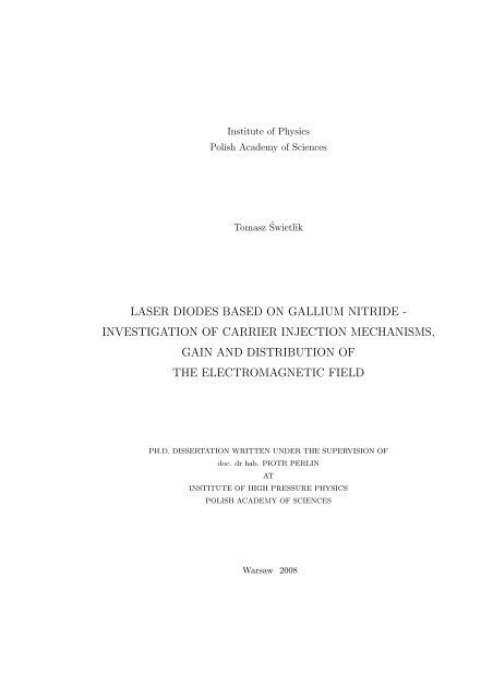
Chapter 2Principles <strong>of</strong> a semic<strong>on</strong>ductor <str<strong>on</strong>g>laser</str<strong>on</strong>g>diode operati<strong>on</strong>2.1 Carrier and phot<strong>on</strong> c<strong>on</strong>finementA semic<strong>on</strong>ductor <str<strong>on</strong>g>laser</str<strong>on</strong>g> is a diode structure created by materials <strong>of</strong> the opposite (negative andpositive) c<strong>on</strong>ductivity types. Once these materials are physically c<strong>on</strong>nected, the majority<strong>carrier</strong>s start to diffuse al<strong>on</strong>g the c<strong>on</strong>centrati<strong>on</strong> gradient leaving behind i<strong>on</strong>ized d<strong>on</strong>ors andacceptors. The space charge formed by i<strong>on</strong>ized dopants sets up the electric field directedoppositely to the directi<strong>on</strong> <strong>of</strong> <strong>carrier</strong> diffusi<strong>on</strong>. Processes <strong>of</strong> drift and diffusi<strong>on</strong> c<strong>on</strong>tinueuntil the equilibrium is reached, which is reflected in a bending <strong>of</strong> c<strong>on</strong>ducti<strong>on</strong> and valenceband pr<strong>of</strong>iles al<strong>on</strong>g the growth axis as a result <strong>of</strong> the formati<strong>on</strong> <strong>of</strong> a c<strong>on</strong>stant Fermi levelthroughout the entire <str<strong>on</strong>g>laser</str<strong>on</strong>g> structure. The applicati<strong>on</strong> <strong>of</strong> the forward bias disturbs theequilibrium. The net movement <strong>of</strong> <strong>carrier</strong>s through the <str<strong>on</strong>g>laser</str<strong>on</strong>g> stack appears. The oppositelycharged <strong>carrier</strong>s generated by the electrical excitati<strong>on</strong> need to recombine radiatively in theactive regi<strong>on</strong> as depicted in Figure 2.1(a).For low injecti<strong>on</strong> currents, light is emitted incoherently in a way that is similar to theLED case. In order to reach lasing acti<strong>on</strong>, <strong>on</strong>e need to supply a sufficiently high c<strong>on</strong>centrati<strong>on</strong><strong>of</strong> <strong>carrier</strong>s within the active regi<strong>on</strong>, which is necessary to induce the populati<strong>on</strong>inversi<strong>on</strong>. Phot<strong>on</strong>s generated this way travel through epitaxial layers and induce further<strong>carrier</strong> recombinati<strong>on</strong> events. Under a sufficiently high excitati<strong>on</strong>, an avalanche-like process<strong>of</strong> phot<strong>on</strong>-stimulated optical recombinati<strong>on</strong> takes place. The device starts to act as anoptical amplifier.
Figure 2.1: Schematic picture <strong>of</strong> the c<strong>on</strong>ducti<strong>on</strong> and valence band pr<strong>of</strong>iles <strong>of</strong> a forwardlybiased p-n juncti<strong>on</strong> (a); refractive index and light intensity distributi<strong>on</strong>s in transverse directi<strong>on</strong><strong>of</strong> a <str<strong>on</strong>g>laser</str<strong>on</strong>g> stack (b).The effect <strong>of</strong> an optical amplificati<strong>on</strong> can be most efficiently accomplished by the utilizati<strong>on</strong><strong>of</strong> a separate c<strong>on</strong>finement heterostructure (SCH). The idea employs a c<strong>on</strong>cept <strong>of</strong> anindependent c<strong>on</strong>finement <strong>of</strong> injected <strong>carrier</strong>s and emitted phot<strong>on</strong>s. In case <strong>of</strong> the <strong>nitride</strong><str<strong>on</strong>g>based</str<strong>on</strong>g>devices, the approach is carried out by a thin (within a nanometer range) active layerc<strong>on</strong>sisting <strong>of</strong> a series <strong>of</strong> thin InGaN quantum wells (QWs) and quantum barriers (QBs),which serve as a <strong>carrier</strong> c<strong>on</strong>finement (See Figure2.1(a)). They are sandwiched between n-and p-type GaN-<str<strong>on</strong>g>based</str<strong>on</strong>g> optical waveguide and AlGaN/GaN superlattices used as claddinglayers for an optical waveguide. Due to an increased excited <strong>carrier</strong> c<strong>on</strong>centrati<strong>on</strong>, theprobability <strong>of</strong> the radiative recombinati<strong>on</strong> also increases. Emitted phot<strong>on</strong>s are effectivelyguided in a transverse directi<strong>on</strong> by a proper refractive index pr<strong>of</strong>ile, which is high in thevicinity <strong>of</strong> QWs and decreases in the directi<strong>on</strong> away from the active regi<strong>on</strong> (Figure 2.1(b)).Res<strong>on</strong>ant cavity established by reflecting facets at both ends <strong>of</strong> the device induces an10
CHAPTER 2.PRINCIPLES OF A SEMICONDUCTOR LASER DIODE OPERATIONFigure 2.2: Schematic picture <strong>of</strong> an (InAl)GaN <str<strong>on</strong>g>laser</str<strong>on</strong>g> diode.optical feedback. These facets are formed by a mechanical cleavage <strong>of</strong> the crystal al<strong>on</strong>g itscrystallographic planes. If a net optical amplificati<strong>on</strong> is large enough to compensate for allpossible optical losses, phot<strong>on</strong>s oscillating back and forth form a steady-state electromagneticwave, which finally emerges out <strong>of</strong> the <str<strong>on</strong>g>laser</str<strong>on</strong>g> device as a coherent optical beam. Aschematic picture <strong>of</strong> a practical realizati<strong>on</strong> <strong>of</strong> a <str<strong>on</strong>g>laser</str<strong>on</strong>g> device is depicted in Figure 2.2. Amore detailed approach will be presented in Chapter 4 to fulfill the need <strong>of</strong> an overview <strong>of</strong>the studied samples.2.2 Carrier injecti<strong>on</strong> and recombinati<strong>on</strong>In every practical case, electrical current applied to device’s c<strong>on</strong>tact electrodes plays a role<strong>of</strong> a source <strong>of</strong> excited <strong>carrier</strong> populati<strong>on</strong> established in the active regi<strong>on</strong>. Efficient <strong>carrier</strong>injecti<strong>on</strong> is <strong>on</strong>e <strong>of</strong> the major factors necessary to approach specific c<strong>on</strong>diti<strong>on</strong>s under whichlasing occurs. After injecti<strong>on</strong>, as a c<strong>on</strong>sequence <strong>of</strong> the intraband <strong>carrier</strong>-<strong>carrier</strong> scattering,excess electr<strong>on</strong>s and holes equilibrate instantly. Even under c<strong>on</strong>diti<strong>on</strong>s <strong>of</strong> dynamic injecti<strong>on</strong>,occupati<strong>on</strong> probabilities <strong>of</strong> ground (E 1 ) and excited states (E 2 ) follow Fermi-Dirac distributi<strong>on</strong>functi<strong>on</strong>s as derived for a populati<strong>on</strong> <strong>of</strong> fermi<strong>on</strong>s under thermal equilibrium. Separateoccupati<strong>on</strong> levels for c<strong>on</strong>ducti<strong>on</strong> (E F C ) and valence band (E F V ) established this way are11
usually separated by a little less than the voltage applied to the p-n juncti<strong>on</strong> (Figure 2.1(a)).1f 1 =exp [ E 1−E F VkT] + 11f 2 =exp [ E 2−E F CkT] + 1(2.2.1)(2.2.2)Charge neutrality principle requires that the total charge density in quantum well or inentire active regi<strong>on</strong> equals zero.Because quantum wells are usually undoped or lightlydoped it can be assumed that electr<strong>on</strong> c<strong>on</strong>centrati<strong>on</strong> (N) equals hole c<strong>on</strong>centrati<strong>on</strong> (P).Thus it is possible to extract informati<strong>on</strong> <strong>on</strong> a <strong>carrier</strong> density dependance <strong>of</strong> recombinati<strong>on</strong>mechanisms <strong>on</strong>ly by tracking solely the injected electr<strong>on</strong> density.2.3 Basic radiative transiti<strong>on</strong>sTemporal dependance <strong>of</strong> the excited electr<strong>on</strong> c<strong>on</strong>centrati<strong>on</strong> can be enclosed in <strong>on</strong>e <strong>carrier</strong>rate equati<strong>on</strong> that takes into c<strong>on</strong>siderati<strong>on</strong> all possible <strong>carrier</strong> recombinati<strong>on</strong> mechanismstaking place in unit active volume per unit time interval (s −1 m −3 ):dNdt= G − R. (2.3.1)Carrier injecti<strong>on</strong> caused by applied electrical voltage enters through generati<strong>on</strong> rate G.Total <strong>carrier</strong> recombinati<strong>on</strong> rate R depends in turn <strong>on</strong> many different recombinati<strong>on</strong> mechanismsc<strong>on</strong>sisting <strong>of</strong> the following recombinati<strong>on</strong> rates: sp<strong>on</strong>taneous recombinati<strong>on</strong> (R sp ),net stimulated recombinati<strong>on</strong> (R st ), n<strong>on</strong>radiative recombinati<strong>on</strong> (R nr ) and <strong>carrier</strong> leakage(R l ).R = R sp + R st + R nr + R l . (2.3.2)The first two terms c<strong>on</strong>tribute c<strong>on</strong>structively to the formati<strong>on</strong> <strong>of</strong> a coherent electromagneticwave. Especially R st which is the main phot<strong>on</strong> generati<strong>on</strong> term above threshold. On theother hand the latter two c<strong>on</strong>stitute a source <strong>of</strong> a <strong>carrier</strong> loss that needs to be efficientlysuppressed as they deteriorate a device’s performance.2.3.1 Sp<strong>on</strong>taneous Emissi<strong>on</strong>Stimulated and sp<strong>on</strong>taneous radiative recombinati<strong>on</strong> processes are <strong>of</strong> pr<strong>of</strong>ound importancein understanding clearly the mechanisms <strong>of</strong> semic<strong>on</strong>ductor gain in <str<strong>on</strong>g>laser</str<strong>on</strong>g> diode. Stimulated12
CHAPTER 2.PRINCIPLES OF A SEMICONDUCTOR LASER DIODE OPERATIONrecombinati<strong>on</strong> occurs under the incidence <strong>of</strong> a real electromagnetic wave, while sp<strong>on</strong>taneousemissi<strong>on</strong> is triggered by a vacuum field oscillati<strong>on</strong>s having a field strength equal to a strength<strong>of</strong> a real electromagnetic wave induced by <strong>on</strong>e real phot<strong>on</strong>. Downward transiti<strong>on</strong>s from excitedto ground state create a new phot<strong>on</strong> into the same optical mode as the stimulating<strong>on</strong>e, no matter whether it is a real or a vacuum-field phot<strong>on</strong>. The newly created phot<strong>on</strong>sappear not <strong>on</strong>ly in the same optical mode but also have the same phase c<strong>on</strong>tributing tothe incident field c<strong>on</strong>structively. As a result, the optical mode can build up as it travelsal<strong>on</strong>g the active regi<strong>on</strong> and forms a coherent wave. Unfortunately, vacuum field phase isnot correlated with phase <strong>of</strong> a real phot<strong>on</strong> field. New phot<strong>on</strong>s introduced through sp<strong>on</strong>taneousemissi<strong>on</strong> have random phases in c<strong>on</strong>tradicti<strong>on</strong> to coherent field created by stimulatedemissi<strong>on</strong>. Additi<strong>on</strong>ally, they are emitted uniformly into every directi<strong>on</strong> <strong>of</strong> a solid angle.As a result, <strong>on</strong>ly a small fracti<strong>on</strong> <strong>of</strong> them propagates al<strong>on</strong>g the waveguiding layers with adesired phase c<strong>on</strong>tributing to the formati<strong>on</strong> <strong>of</strong> the lasing mode <strong>of</strong> the cavity. In order totake into account a fracti<strong>on</strong> <strong>of</strong> a total amount <strong>of</strong> sp<strong>on</strong>taneous emissi<strong>on</strong> that reinforces themode <strong>of</strong> interest, the sp<strong>on</strong>taneous emissi<strong>on</strong> factor β sp is introduced which is roughly equalto the reciprocal <strong>of</strong> the total number <strong>of</strong> all possible modes in a res<strong>on</strong>ant cavity.Sp<strong>on</strong>taneous emissi<strong>on</strong> spectrum is peaked just above the bandgap energy (because injectedelectr<strong>on</strong>s and holes mostly gather at the band edges) and in case <strong>of</strong> a n<strong>on</strong>degeneratesemic<strong>on</strong>ductor decays towards higher energies following the tail <strong>of</strong> the Boltzmann distributi<strong>on</strong>functi<strong>on</strong>. As the injected <strong>carrier</strong> density is being increased to reach higher excitati<strong>on</strong>level <strong>of</strong> the material, sp<strong>on</strong>taneous emissi<strong>on</strong> rate also increases inevitably. This process isimportant and needs to be c<strong>on</strong>sidered because for each phot<strong>on</strong> emitted sp<strong>on</strong>taneously a new<strong>carrier</strong> needs to be injected into the active regi<strong>on</strong>. In case <strong>of</strong> devices <str<strong>on</strong>g>based</str<strong>on</strong>g> <strong>on</strong> wide bandgapmaterials this mechanism <strong>of</strong> <strong>carrier</strong> recombinati<strong>on</strong> represents the largest c<strong>on</strong>tributi<strong>on</strong> to thetotal amount <strong>of</strong> current that needs to be injected in order to reach a desired level <strong>of</strong> materialexcitati<strong>on</strong>. Analysis <strong>of</strong> total sp<strong>on</strong>taneous recombinati<strong>on</strong> rate that takes into accountcomp<strong>on</strong>ents from all possible optical modes allows <strong>on</strong>e to determine the radiative part <strong>of</strong>the injected current.Thus stimulated emissi<strong>on</strong> becomes the major recombinati<strong>on</strong> mechanism supplying phot<strong>on</strong>sinto the lasing mode. However, the sp<strong>on</strong>taneous emissi<strong>on</strong> cannot be completely ignored.Although it is a source <strong>of</strong> a relatively small number <strong>of</strong> phot<strong>on</strong>s compared to the13
overall amount <strong>of</strong> stimulated emissi<strong>on</strong> phot<strong>on</strong>s (β sp equals 10 −4 - 10 −5 depending <strong>on</strong> a materialsystem and active regi<strong>on</strong> volume), their populati<strong>on</strong> is large enough to be resp<strong>on</strong>siblefor deteriorati<strong>on</strong> <strong>of</strong> a complete coherence in a <str<strong>on</strong>g>laser</str<strong>on</strong>g>, inducing relative intensity noise - animportant parameter in all data storage applicati<strong>on</strong>s.2.3.2 Stimulated Emissi<strong>on</strong>There are two mechanisms <strong>of</strong> the stimulated recombinati<strong>on</strong> that have to be c<strong>on</strong>sideredjointly: stimulated absorpti<strong>on</strong> and emissi<strong>on</strong>. Phot<strong>on</strong>s with given energy hν induce upwardand downward transiti<strong>on</strong>s <strong>on</strong>ly between those electr<strong>on</strong>ic state pairs which c<strong>on</strong>verse both:energy (E 2 - E 1 = E 21 ) and momentum (k 1 = k 2 ) implying that direct transiti<strong>on</strong>s in E − kspace are preferred.Both mechanisms compete with each other since <strong>on</strong>e <strong>of</strong> them generates phot<strong>on</strong>s intoa given mode while the other takes them away. These processes occur <strong>on</strong>ly between filledinitial and empty final states which are taken into c<strong>on</strong>siderati<strong>on</strong> through Fermi distributi<strong>on</strong>functi<strong>on</strong>s f 1 and f 2 . The transiti<strong>on</strong>s are described by the rates <strong>of</strong> stimulated absorpti<strong>on</strong> (R 12 )and emissi<strong>on</strong> (R 21 ) per unit time per unit active volume (s −1 m −3 ), respectively. Thus it isthe most c<strong>on</strong>venient to introduce net stimulated recombinati<strong>on</strong> rate:R st = R 21 − R 12 = R r (f 2 − f 1 ), (2.3.3)where R r represents the total radiative rate that would exist if all state pairs were availableto participate in a transiti<strong>on</strong> at a given energy. R r gives the number <strong>of</strong> transiti<strong>on</strong>s per unitactive volume occurring in a unit time interval as described by Fermi’s Golden Rule forsemic<strong>on</strong>ductor:R r = 2π |H′ 21| 2 ρ r (E 21 ) (2.3.4)R r is proporti<strong>on</strong>al to the density <strong>of</strong> allowed transiti<strong>on</strong> pairs existing at transiti<strong>on</strong> energy <strong>of</strong>interest given by the reduced density <strong>of</strong> states ρ r . R r depends mainly <strong>on</strong> the spatial overlap<strong>of</strong> initial (Ψ 1 ) and final (Ψ 2 ) electr<strong>on</strong>ic wavefuncti<strong>on</strong>s under the time-harm<strong>on</strong>ic perturbati<strong>on</strong>(H 21 ′ ) induced by a stimulating electromagnetic wave. Since all possible electr<strong>on</strong>ic statesform orthog<strong>on</strong>al set <strong>of</strong> wavefuncti<strong>on</strong>s mainly those with an overlap integral close to unitytake part in the transiti<strong>on</strong>. Although a perfect orthog<strong>on</strong>ality is disturbed by differences inelectr<strong>on</strong> and hole effective masses and barrier heights in a c<strong>on</strong>ducti<strong>on</strong> and valence bands,14
CHAPTER 2.PRINCIPLES OF A SEMICONDUCTOR LASER DIODE OPERATIONwavefuncti<strong>on</strong> overlap leads to the k-selecti<strong>on</strong> rule which requires that an electr<strong>on</strong> in theinitial and the final energetic state propagates al<strong>on</strong>g the same directi<strong>on</strong>.The two possible transiti<strong>on</strong> states must be in res<strong>on</strong>ance with oscillati<strong>on</strong>s <strong>of</strong> incidentelectromagnetic wave. The strength <strong>of</strong> an interacti<strong>on</strong> between them is determined by thematrix element |H 21 ′ |2 defined as:|H 21| ′ 2 ∝ | < Ψ 2 |ê · p|Ψ 1 > | 2 (2.3.5)It depends not <strong>on</strong>ly <strong>on</strong> the envelope wavefuncti<strong>on</strong>s <strong>of</strong> initial and final electr<strong>on</strong>ic statesand their overlap but also <strong>on</strong> the polarizati<strong>on</strong> <strong>of</strong> incident light provided that the materialhas a preferred axis <strong>of</strong> symmetry. Particular symmetries <strong>of</strong> the c<strong>on</strong>ducti<strong>on</strong> and valenceband Bloch functi<strong>on</strong>s in quantum well <str<strong>on</strong>g>laser</str<strong>on</strong>g>s cause that the interacti<strong>on</strong> between c<strong>on</strong>ducti<strong>on</strong>and heavy-hole states is much str<strong>on</strong>ger for electric fields polarized in the plane <strong>of</strong> the wellthan in the directi<strong>on</strong> perpendicular to it. As a result about 90% <strong>of</strong> stimulated emissi<strong>on</strong> in<strong>nitride</strong>-<str<strong>on</strong>g>based</str<strong>on</strong>g> LDs is coupled into the TE mode polarized in the juncti<strong>on</strong> plane [21].2.4 Material gainWhen a material is excited by an external source injecting excess <strong>carrier</strong> populati<strong>on</strong>, thebalance between stimulated absorpti<strong>on</strong> and emissi<strong>on</strong> changes. At some level <strong>of</strong> injecti<strong>on</strong>emissi<strong>on</strong> processes prevail over absorpti<strong>on</strong>. As a result material gain appears which isreflected in the <strong>on</strong>set <strong>of</strong> optical amplificati<strong>on</strong>. The phot<strong>on</strong> density propagating al<strong>on</strong>g somedirecti<strong>on</strong> in a material is subject to the proporti<strong>on</strong>al growth in populati<strong>on</strong> over a givendistance.C<strong>on</strong>sidering the stimulated emissi<strong>on</strong> and absorpti<strong>on</strong> rates at a given transiti<strong>on</strong> energy(E 21 ) <strong>on</strong>e can take into account the ratio between them:R 21= exp[ ∆E F − E 21] (2.4.1)R 12 kTNet stimulated emissi<strong>on</strong> rate and c<strong>on</strong>sequently optical gain will become positive when separati<strong>on</strong><strong>of</strong> Fermi levels (∆E F ) will be larger than the transiti<strong>on</strong> energy <strong>of</strong> interest E 21 . Thusthe following relati<strong>on</strong> needs to be satisfied:∆E F < E 21 < E g , (2.4.2)15
implying that the voltage across the juncti<strong>on</strong> must be grater than the bandgap to achievegain in the active regi<strong>on</strong>.Using Fermi’s Golden Rule material gain at a given transiti<strong>on</strong> energy g 21 can be describedby:g 21 = 2π |H ′ 21 |2v g N pρ r (E 21 )(f 2 − f 1 ) (2.4.3)It is possible to divide the origin <strong>of</strong> the optical gain into two comp<strong>on</strong>ents. One <strong>of</strong> themreflects injecti<strong>on</strong> level through Fermi distributi<strong>on</strong> functi<strong>on</strong>s (f 1 and f 2 ). The other is strictlymaterial dependent and relies <strong>on</strong>:ˆ incident perturbati<strong>on</strong> to the system Hamilt<strong>on</strong>ian (H’ 21 ),ˆ phot<strong>on</strong> populati<strong>on</strong> in a c<strong>on</strong>sidered mode (N p ),ˆ the group velocity (v g ) <strong>of</strong> electromagnetic wave.The material-dependent comp<strong>on</strong>ent defines the maximum material gain possible when <strong>carrier</strong>populati<strong>on</strong> is totally inverted (f 1 =0 and f 2 =1). In case <strong>of</strong> <strong>nitride</strong>s the maximum value<strong>of</strong> material gain reaches about 10 4 cm −1 .Usually <strong>on</strong>ly about 30% <strong>of</strong> a maximum material gain is necessary to obtain lasing.Selecti<strong>on</strong> rules arising from the symmetry and the overlap between wavefuncti<strong>on</strong> envelopessuggest that transiti<strong>on</strong>s between state pairs <strong>of</strong> the same number are preferred and yield adominant c<strong>on</strong>tributi<strong>on</strong> to the total gain spectrum. For quantum well <str<strong>on</strong>g>laser</str<strong>on</strong>g>s usually stateswith n=1 are <strong>of</strong> the highest importance.The total gain at a given transiti<strong>on</strong> energy E 21 is a result <strong>of</strong> c<strong>on</strong>tributing transiti<strong>on</strong>sbetween all possible state pairs separated by this energy. It occurs <strong>on</strong>ly under populati<strong>on</strong>inversi<strong>on</strong> c<strong>on</strong>diti<strong>on</strong>s which require that f 2 > f 1 .Exact positi<strong>on</strong>s <strong>of</strong> quasi-Fermi levels forc<strong>on</strong>ducti<strong>on</strong> and valence bands does not play a significant role. What really matters is themagnitude <strong>of</strong> their separati<strong>on</strong>.2.5 Radiative recombinati<strong>on</strong> mechanisms in <strong>nitride</strong>sA comm<strong>on</strong>ly used active regi<strong>on</strong> <strong>of</strong> <strong>nitride</strong>-<str<strong>on</strong>g>based</str<strong>on</strong>g> emitters c<strong>on</strong>sist <strong>of</strong> quantum wells and barriers<str<strong>on</strong>g>based</str<strong>on</strong>g> <strong>on</strong> Ga-rich In x Ga 1−x N alloy with indium c<strong>on</strong>centrati<strong>on</strong>s ranging mainly between16
CHAPTER 2.PRINCIPLES OF A SEMICONDUCTOR LASER DIODE OPERATIONx=0.02 and x=0.2 depending <strong>on</strong> the desired emissi<strong>on</strong> energy and <strong>carrier</strong> c<strong>on</strong>finement. Because<strong>of</strong> the lack <strong>of</strong> a lattice-matched substrate the early devices suffered from extremelylarge threading dislocati<strong>on</strong> densities ranging from 10 9 cm −2 to 10 10 cm −2 [22, 23]. Nowadaysthey are reduced down to 10 5 - 10 6 cm −2 because <strong>of</strong> the usage <strong>of</strong> overgrowth [24] andhigh pressure growth [25] techniques. What would definitely hinder an effective radiativeemissi<strong>on</strong> in AlGaAs- and AlInGaP-<str<strong>on</strong>g>based</str<strong>on</strong>g> devices turned out not to be as much critical fora new material system. Radiative efficiency <strong>of</strong> InGaN emitters shows superiority over otherIII-V semic<strong>on</strong>ductor compounds. In order to explain insensitivity <strong>of</strong> radiative recombinati<strong>on</strong>processes to structural defects <strong>of</strong> the material different phenomena have been proposed.The most widely accepted <strong>on</strong>e c<strong>on</strong>cerns In inhomogeneities as a major <strong>carrier</strong> localizati<strong>on</strong>effect [23]. Its origin is attributed to the low miscibility <strong>of</strong> In in GaN resulting in clustering<strong>of</strong> In which causes difficulties in obtaining homogenous Ga-rich InGaN layers [26]. Spatialfluctuati<strong>on</strong>s <strong>of</strong> the In c<strong>on</strong>tent lead to band pr<strong>of</strong>ile inhomogeneities that induce <strong>carrier</strong>c<strong>on</strong>finement and isolati<strong>on</strong> from n<strong>on</strong>radiative recombinati<strong>on</strong> centers. The strength <strong>of</strong> thiseffect is reflected in magnitude <strong>of</strong> photoluminescence and <strong>carrier</strong> decay times which are <strong>on</strong>lyslightly influenced by changes in a threading dislocati<strong>on</strong> density [27]. The same effect hasbeen argued to be caused by potential changes because <strong>of</strong> well thickness variati<strong>on</strong>s or byband bending at V-shaped defects [28].Deviati<strong>on</strong>s from designed QW thickness and In c<strong>on</strong>tent increase additi<strong>on</strong>ally the density<strong>of</strong> available states which give rise to inhomogeneous broadening <strong>of</strong> a gain curve throughappearance <strong>of</strong> band-tail states. With elevated <strong>carrier</strong> injecti<strong>on</strong> the band-tail states togetherwith the lowest c<strong>on</strong>ducti<strong>on</strong> band states become populated. Additi<strong>on</strong>ally, screening <strong>of</strong> internalelectric fields takes place. As a combined effect <strong>of</strong> these two phenomena a blueshift in theemissi<strong>on</strong> energy appears. On the other hand Coulomb effects redshift the emissi<strong>on</strong> energymostly due to bandgap renormalizati<strong>on</strong> with a smaller impact <strong>of</strong> dephasing and screening[29]. The spectral shift <strong>of</strong> the resulting gain curves is a net effect <strong>of</strong> these processes andwill be subject to the analysis in the next chapters.Intensified experimental work devoted to identificati<strong>on</strong> <strong>of</strong> the major radiative recombinati<strong>on</strong>processes has been carried out so far. Because <strong>of</strong> the lack <strong>of</strong> heavy doping within quantumwells the main radiative processes involved in the generati<strong>on</strong> <strong>of</strong> light are band-to-bandtransiti<strong>on</strong>s. Their specific features are governed by the excitati<strong>on</strong> level. It is comm<strong>on</strong>ly17
agreed that the origin <strong>of</strong> sp<strong>on</strong>taneous emissi<strong>on</strong> comes from recombinati<strong>on</strong> <strong>of</strong> excit<strong>on</strong>s localizedat bandedge potential minima [23] introduced by In clustering. Compositi<strong>on</strong>al imperfecti<strong>on</strong>sinduce fluctuati<strong>on</strong> <strong>of</strong> excit<strong>on</strong>ic transiti<strong>on</strong> energy. They are reported to remainin the range between 30 meV [30] and 250 meV [31] in different samples which is c<strong>on</strong>siderablylarger than 10 meV expected for a simple random alloy [32]. As a result theexcit<strong>on</strong> transiti<strong>on</strong> energy observed even at room temperature can occur below the lowestn=1 quantized level [31]. Although excit<strong>on</strong>ic behavior has been theoretically predicted todisappear at elevated injecti<strong>on</strong> levels [33, 34] and the lasing acti<strong>on</strong> should originate fromrecombinati<strong>on</strong> <strong>of</strong> electr<strong>on</strong>-hole plasma [35], it is difficult to verify this fact experimentally.The combined effects <strong>of</strong> bandfilling, screening <strong>of</strong> str<strong>on</strong>g sp<strong>on</strong>taneous and piezoelectric fieldsand Coulomb interacti<strong>on</strong>s together with the band-gap renormalizati<strong>on</strong> form a complex set<strong>of</strong> phenomena that define the optical characteristics <strong>of</strong> InGaN-<str<strong>on</strong>g>based</str<strong>on</strong>g> quantum wells. Theycannot be analyzed separately. C<strong>on</strong>sidered together they effectively mask the origin <strong>of</strong>stimulated emissi<strong>on</strong> in <strong>nitride</strong>s. Despite the initial attributi<strong>on</strong> <strong>of</strong> lasing to recombinati<strong>on</strong> <strong>of</strong>deeply localized [36] or free excit<strong>on</strong>s [37], the latest results <str<strong>on</strong>g>based</str<strong>on</strong>g> <strong>on</strong> the detailed analysis<strong>of</strong> the sp<strong>on</strong>taneous electroluminescence spectra tend to assume that excit<strong>on</strong> pairs becomeunstable at threshold [38]. The 60 meV excit<strong>on</strong> binding energy predicted for low <strong>carrier</strong>density in quantum well [39] becomes c<strong>on</strong>siderably reduced while approaching lasing dueto bandfilling and screening effects. Thus the assumpti<strong>on</strong> suggesting that the free electr<strong>on</strong>holeplasma yields the major c<strong>on</strong>tributi<strong>on</strong> to lasing c<strong>on</strong>firms the early reports made byNakamura et al. [40]. However, it is still not clear whether the optical properties <strong>of</strong> <strong>nitride</strong>devices should be explained <strong>on</strong> grounds <strong>of</strong> quantum well physics or rather by gain modelsassuming the formati<strong>on</strong> <strong>of</strong> quantum-dot-like structures [41].2.6 Optical modes <strong>of</strong> a res<strong>on</strong>ant cavityOptical energy <strong>of</strong> a diode <str<strong>on</strong>g>laser</str<strong>on</strong>g> is stored in a standing electromagnetic wave <strong>of</strong> a res<strong>on</strong>antcavity. The res<strong>on</strong>ant mode, originating from radiative recombinati<strong>on</strong> within InGaN quantumwells, is guided by a GaN-<str<strong>on</strong>g>based</str<strong>on</strong>g> waveguide and Al 0.16 Ga 0.84 N/GaN strained layersupperlattice cladding. These layers account for transverse (across the epitaxial layers) opticalc<strong>on</strong>finement. Lateral c<strong>on</strong>finement (parallel to the juncti<strong>on</strong> plane) is induced by shallowetching (down to the middle <strong>of</strong> a p-type waveguide) to form a mesa stripe (see Figure 2.2).18
CHAPTER 2.PRINCIPLES OF A SEMICONDUCTOR LASER DIODE OPERATIONElectrically insulating layer <strong>of</strong> SiO 2 deposited <strong>on</strong> both sides <strong>of</strong> the mesa stripe limits the<strong>carrier</strong> injecti<strong>on</strong> <strong>on</strong>ly to this regi<strong>on</strong>, reduces current spreading and defines the axis and thewidth <strong>of</strong> a res<strong>on</strong>ant cavity. Since a charge flow is limited <strong>on</strong>ly to a narrow stripe regi<strong>on</strong>, socalled gain guiding appears. Although a gain guided mode has a diverging wavefr<strong>on</strong>t [42],a spatial variati<strong>on</strong> in a distributi<strong>on</strong> <strong>of</strong> injected <strong>carrier</strong>s induces a c<strong>on</strong>stant mode width in alateral directi<strong>on</strong>. Increased losses bey<strong>on</strong>d the border between electrically excited and unexcitedregi<strong>on</strong>s keep a semic<strong>on</strong>ductor material below the optical transparency level. Spatiallyvarying distributi<strong>on</strong> <strong>of</strong> injected <strong>carrier</strong>s defines a gain stripe below the p-type c<strong>on</strong>tact electrodeal<strong>on</strong>g which a guided mode can be sustained. The effect <strong>of</strong> a lateral c<strong>on</strong>finement isadditi<strong>on</strong>ally strengthened by the mesa stripe inducing a weak index guiding, which makesuse <strong>of</strong> a difference between refractive indices <strong>of</strong> a GaN waveguide and surrounding SiO 2layer.The analysis originating from Maxwell’s theory leads to the derivati<strong>on</strong> <strong>of</strong> time- andspace-dependent wave equati<strong>on</strong>:∇ 2 E = µε ∂2 E∂t 2 (2.6.1)In case <strong>of</strong> a semic<strong>on</strong>ductor <str<strong>on</strong>g>laser</str<strong>on</strong>g>, this relati<strong>on</strong> can be satisfied by time-harm<strong>on</strong>ic field propagatingin a dielectric waveguide al<strong>on</strong>g the res<strong>on</strong>ator directi<strong>on</strong> oriented parallel to z-axis:E(x, y, z, t) = ê i E 0 U(x, y) e i(ωt−e βz)(2.6.2)The unit vector ê i defines either TE or TM polarizati<strong>on</strong>, E 0 gives the wave amplitude inunits <strong>of</strong> volts and U(x,y) describes the scalar normalized electric field pr<strong>of</strong>ile in the planeperpendicular to the propagati<strong>on</strong> directi<strong>on</strong>. Optical gain and internal propagati<strong>on</strong> loss aretaken into account through the complex propagati<strong>on</strong> c<strong>on</strong>stant ˜β.Once equati<strong>on</strong> 2.6.2 is plugged into 2.6.1, it straightforwardly appears, that the electricfield distributi<strong>on</strong> U(x,y) must satisfy a time-independent relati<strong>on</strong>:∇ 2 U(x, y) + [ ñ 2 k0 2 − ˜β 2 ] U(x, y) = 0 (2.6.3)where k 0 and ñ stand for the free-space wave vector and the effective refractive index <strong>of</strong> agiven mode, respectively. All modes are unique soluti<strong>on</strong>s <strong>of</strong> Maxwell’s equati<strong>on</strong>s, satisfyingc<strong>on</strong>strains imposed by c<strong>on</strong>tinuity c<strong>on</strong>diti<strong>on</strong>s <strong>of</strong> the tangential fields at the boundaries. ThusU(x,y) describes the distributi<strong>on</strong> <strong>of</strong> the intensity pr<strong>of</strong>ile <strong>of</strong> a standing electromagnetic wave19
in a <str<strong>on</strong>g>laser</str<strong>on</strong>g> cavity. In every practical case the transverse field pr<strong>of</strong>ile <strong>of</strong> a guided mode <strong>of</strong>interest has a maximum at the active regi<strong>on</strong> and takes the form <strong>of</strong> evanescent waves as thedistance from the quantum wells increases (Figure 2.1).In order to account for the reducti<strong>on</strong> in gain induced by the spreading <strong>of</strong> the modeaway from the active regi<strong>on</strong>, optical c<strong>on</strong>finement factor needs to be defined as a spatialoverlap <strong>of</strong> the volume occupied by injected <strong>carrier</strong>s (i.e. quantum wells, where the actualoptical amplificati<strong>on</strong> takes place) to the entire volume c<strong>on</strong>taining the electromagnetic wave.Since the phot<strong>on</strong> field <strong>of</strong> edge emitting <str<strong>on</strong>g>laser</str<strong>on</strong>g>s almost totally fills the res<strong>on</strong>ator al<strong>on</strong>g itsaxis, the integrati<strong>on</strong> in this directi<strong>on</strong> can be omitted as it yields a unity and the opticalc<strong>on</strong>finement c<strong>on</strong>sists in the first approximati<strong>on</strong> <strong>of</strong> transverse and lateral comp<strong>on</strong>ent. Thusa three-dimensi<strong>on</strong>al relati<strong>on</strong> reduces to:Γ =∫ wx∫ wy0∫ +∞−∞0|U(x, y)| 2 dx dy∫ +∞−∞ |U(x, y)| 2 dx dy(2.6.4)The differences <strong>of</strong> refractive index values between the subsequent comp<strong>on</strong>ents <strong>of</strong> a multilayereddielectric waveguide are in a range <strong>of</strong> 1 percent. They account for a relatively weakwaveguiding and significant mode spreading. The optical c<strong>on</strong>finement typically remainsnot larger than a few percent. This relatively low value is enough to reach lasing for areas<strong>on</strong>able range <strong>of</strong> injecti<strong>on</strong> currents. However, care needs to be taken in order to get adetailed insight into the optical properties <strong>of</strong> the waveguide.2.7 Threshold for lasing acti<strong>on</strong>Lasing acti<strong>on</strong> for a given mode can be reached <strong>on</strong>ly when both mirror loss α m as well asinternal propagati<strong>on</strong> loss < α i > are compensated. This means that at threshold the electricfield E described by Equati<strong>on</strong> 2.6.2 should replicate itself after <strong>on</strong>e round-trip within thecavity. Practically this c<strong>on</strong>diti<strong>on</strong> requires that E(0)=E(2L), defining the threshold relati<strong>on</strong>between material gain g mat , optical c<strong>on</strong>finement Γ, res<strong>on</strong>ator length L and mirror reflectivitycoefficients r 1 and r 2 .Γ g th mat = < α i > + 1 L ln 1r 1 r 2(2.7.1)If the injecti<strong>on</strong> current is increased above its threshold value, <strong>carrier</strong> density N and materialgain g mat (related to N m<strong>on</strong>ot<strong>on</strong>ically) increase temporarily as well. The amount <strong>of</strong> the20
CHAPTER 2.PRINCIPLES OF A SEMICONDUCTOR LASER DIODE OPERATIONnet stimulated recombinati<strong>on</strong> rate R st also increases instantly reducing finally the abovethreshold<strong>carrier</strong> c<strong>on</strong>centrati<strong>on</strong> and the material gain down to their threshold values. Allexcess <strong>carrier</strong>s are c<strong>on</strong>sumed by the stimulated emissi<strong>on</strong> and corresp<strong>on</strong>ding recombinati<strong>on</strong>energy appears as increased optical power at <str<strong>on</strong>g>laser</str<strong>on</strong>g> output. As a result gain and <strong>carrier</strong>density clamp at their threshold values with oscillating changes in the range <strong>of</strong> nanosec<strong>on</strong>ds.If it were not for the fact that the material gain stays c<strong>on</strong>stant for any given current abovethreshold, the optical power within the res<strong>on</strong>ator would increase without bounds. Theprinciple <strong>of</strong> energy c<strong>on</strong>servati<strong>on</strong> would be violated.2.8 Laser characteristics above thresholdOnce the <strong>carrier</strong> injecti<strong>on</strong> reaches the threshold level, a coherent electromagnetic waveemerges out <strong>of</strong> the res<strong>on</strong>ant cavity evidencing the dominant <strong>on</strong>set <strong>of</strong> the stimulated emissi<strong>on</strong>.In order to establish the lasing acti<strong>on</strong> in c<strong>on</strong>tinuous wave regime, input electrical power atthreshold should be minimized. Reduced device heating and degradati<strong>on</strong> can be achievedby maximizing the injecti<strong>on</strong> efficiency. Ideally, the entire injected <strong>carrier</strong> populati<strong>on</strong> shouldrecombine in the active regi<strong>on</strong> and c<strong>on</strong>vert into phot<strong>on</strong>s. In a real device <strong>carrier</strong>s aresubject to the current leakage out <strong>of</strong> the active regi<strong>on</strong> followed by recombinati<strong>on</strong> events(either radiative or n<strong>on</strong>radiative) that does not c<strong>on</strong>tribute to the cavity mode.Although theoretically <strong>carrier</strong> c<strong>on</strong>centrati<strong>on</strong> and material gain should remain pinnedto their threshold values, inhomogeneities in <strong>carrier</strong> injecti<strong>on</strong> and internal loss distributi<strong>on</strong>observed in real devices introduce n<strong>on</strong>-uniformities <strong>of</strong> threshold c<strong>on</strong>diti<strong>on</strong>s throughout theentire active regi<strong>on</strong>. Thus the number <strong>of</strong> <strong>carrier</strong>s that recombine within the active regi<strong>on</strong>is not equal to the total number <strong>of</strong> <strong>carrier</strong>s injected into the device. The fracti<strong>on</strong> <strong>of</strong> theabove-threshold current that results in stimulated emissi<strong>on</strong> is usually defined as the internalquantum efficiency η i .To assure the maximum possible <strong>carrier</strong> injecti<strong>on</strong> level modern diode <str<strong>on</strong>g>laser</str<strong>on</strong>g> have evolvedto heterostructure devices c<strong>on</strong>sisting <strong>of</strong> adjacent epitaxial layers formed by compounds <strong>of</strong>similar lattice c<strong>on</strong>stant and crystal symmetry but having different bandgaps. An alloy withthe lowest bandgap is used within a depleti<strong>on</strong> regi<strong>on</strong> <strong>of</strong> a diode to form a quantum-well-<str<strong>on</strong>g>based</str<strong>on</strong>g>active regi<strong>on</strong> which c<strong>on</strong>fines injected electr<strong>on</strong>s and holes, increases <strong>carrier</strong> c<strong>on</strong>centrati<strong>on</strong> andimproves radiative recombinati<strong>on</strong> rates leading to enhanced optical gain and reduced <strong>carrier</strong>21
losses. As a result lower operating current densities can be achieved this way.As it can be derived from the <strong>carrier</strong>- and phot<strong>on</strong>-rate equati<strong>on</strong>s [43] the relati<strong>on</strong> betweenoutput power P out versus driving current I above threshold I th (so called L-I characteristic)can be enclosed in the equati<strong>on</strong> taking into account injecti<strong>on</strong> and radiative efficiencies,internal propagati<strong>on</strong> and mirror loss and emissi<strong>on</strong> energy hν.α mP out = η i () hν< α i > +α m q (I − I th) (2.8.1)A typical light-current and voltage-current curves and the emissi<strong>on</strong> spectra <strong>of</strong> a CWoperated<str<strong>on</strong>g>laser</str<strong>on</strong>g> device are depicted in Figure 2.3(a) and (b), respectively. The device wasstabilized at 18‰ by a thermoelectric cooler.Figure 2.3: Typical light-current and voltage-current curves (a) and the emissi<strong>on</strong> spectra(b) <strong>of</strong> a CW-operated LD.The output power above threshold is a linear functi<strong>on</strong> <strong>of</strong> current. Ideally, if all <strong>of</strong> the<strong>carrier</strong>s recombined radiatively in quantum wells and all internal propagati<strong>on</strong> losses wereeliminated, the L-I slope would reach about 3 W/A for the emissi<strong>on</strong> energy <strong>of</strong> GaN-<str<strong>on</strong>g>based</str<strong>on</strong>g>device close to 400 nm. The linearity <strong>of</strong> the <str<strong>on</strong>g>laser</str<strong>on</strong>g> output can be however broken when spatialinhomogeneities in <strong>carrier</strong> and temperature distributi<strong>on</strong> induce changes in effective index<strong>of</strong> refracti<strong>on</strong> forcing the switch between the res<strong>on</strong>ator modes reflected by the appearance22
CHAPTER 2.PRINCIPLES OF A SEMICONDUCTOR LASER DIODE OPERATION<strong>of</strong> kink in the L-I curve. What is even more important, if the excess heat generated bythe current flow cannot be efficiently dissipated by the cooling system, thermal roll-overappears. At high temperature the potential barriers in the active regi<strong>on</strong> do not c<strong>on</strong>fine<strong>carrier</strong>s efficiently any more and thermal energy allows them to escape out <strong>of</strong> the quantumwells. The deteriorati<strong>on</strong> in the output power appears.2.9 Near-field and far-field patternsIn an ideal situati<strong>on</strong> <strong>of</strong> a uniform and real-index waveguide, the guided electromagnetic wavepropagating al<strong>on</strong>g the res<strong>on</strong>ator axis has a form <strong>of</strong> a planar wave-fr<strong>on</strong>t (Equati<strong>on</strong> 2.6.2) witha field distributi<strong>on</strong> U(x, y) <strong>on</strong> a <str<strong>on</strong>g>laser</str<strong>on</strong>g> facet. As the wave emerges out <strong>of</strong> the cavity, it diffractsinto the air, where it is usually captured by the external optics after traveling some distance.Diffracti<strong>on</strong> theory refers to a planar field <strong>on</strong> a <str<strong>on</strong>g>laser</str<strong>on</strong>g> facet as a near field. Near field wavesare approximately planar, but gradually start to exhibit a c<strong>on</strong>siderable curvature. Somecritical distance away from the facet, usually about w2λ, where w is the spatial dimensi<strong>on</strong> <strong>of</strong>a source emitting radiati<strong>on</strong> <strong>of</strong> a given wavelength λ, planar waves diffract completely andtransform into field <strong>of</strong> a spherical geometry referred-to as a far field.According to an approach introduced originally by Huygen, each area element at theemitting facet is a source <strong>of</strong> a spherical ’wavelet’, which propagates into the air and c<strong>on</strong>tributesto the overall diffracti<strong>on</strong> pattern. The field is a superpositi<strong>on</strong> <strong>of</strong> periodic functi<strong>on</strong>s<strong>of</strong> different periods and orientati<strong>on</strong>s. It can be expanded into propagating and evanescentwaves [44]. The amount <strong>of</strong> the evanescent waves depend <strong>on</strong> the amount <strong>of</strong> details in the fielddistributi<strong>on</strong> U(x,y), that are smaller than the incident wavelength. The <strong>on</strong>-axis wave vectorcomp<strong>on</strong>ent <strong>of</strong> any given evanescent wave is imaginary. For this reas<strong>on</strong> such waves propagatemainly in x-y plane and they are absent in the far-field picture. The smaller the detail, thegreater weight <strong>of</strong> the evanescent distributi<strong>on</strong> in the <strong>on</strong>-axis directi<strong>on</strong>. C<strong>on</strong>sequently, the finepeculiarities <strong>of</strong> the <strong>on</strong>-facet field distributi<strong>on</strong> are unresolvable from the distance larger thana few nanometers. They are, however, critically important in a process <strong>of</strong> optimizing theproperties <strong>of</strong> the waveguide, as they give a picture <strong>of</strong> a guided mode shape and its evoluti<strong>on</strong>in time. Figure 2.4 depicts example near-field and far-field intensity pr<strong>of</strong>iles collected by anear-field optical microscope. Details <strong>of</strong> such an analysis will be given in Chapter 8. Oncethe spatial near-field distributi<strong>on</strong> U(x,y) is known, the angular far-field intensity pr<strong>of</strong>ile can23
Figure 2.4: Examples <strong>of</strong> near-field pattern and transverse far-field pr<strong>of</strong>ile collected by nearfieldoptical microscope overlayed <strong>on</strong> an SEM image <strong>of</strong> a <str<strong>on</strong>g>laser</str<strong>on</strong>g> facet.be deduced using the designati<strong>on</strong>s made in Figure 2.4 [43]:∫ ∫U F (θ r ) = U(x, y) e−ikr[ i r λ cosθ r]dxdy (2.9.1)In case <strong>of</strong> in-plane edge-emitting <str<strong>on</strong>g>laser</str<strong>on</strong>g>s dimensi<strong>on</strong>s <strong>of</strong> the waveguide in transverse directi<strong>on</strong>are much smaller than the ridge width <strong>of</strong> the mesa stripe. As a result the angular spread <strong>of</strong>the far field in lateral and transverse directi<strong>on</strong>s is c<strong>on</strong>siderably asymmetric approaching 9 ◦and 25 ◦ <strong>of</strong>f the res<strong>on</strong>ator axis, respectively [45]. Although the angular intensity spectrumfollows the elliptical distributi<strong>on</strong>, Equati<strong>on</strong> 2.9.1 indicates, that the emitted beam does notloose its spherical symmetry as it propagates in space.The most important practical applicati<strong>on</strong>s require stability and uniformity <strong>of</strong> the guidedelectromagnetic wave. Chapter 8 will present the results <strong>of</strong> the analysis regarding the spacialand temporal behavior <strong>of</strong> res<strong>on</strong>ant cavity modes, which was carried out by means <strong>of</strong> a timeresolvedscanning near-field optical microscopy.A detailed analysis <strong>of</strong> the waveguidingproperties <strong>of</strong> the <str<strong>on</strong>g>laser</str<strong>on</strong>g> structure as well as the evoluti<strong>on</strong> <strong>of</strong> the near-field into the far-fieldc<strong>on</strong>stitute a powerful tool capable <strong>of</strong> examining the efficiency <strong>of</strong> a given <str<strong>on</strong>g>laser</str<strong>on</strong>g> design, as itwill be presented later <strong>on</strong>.24
Chapter 3Challenges <strong>of</strong> the <strong>nitride</strong>-<str<strong>on</strong>g>based</str<strong>on</strong>g><str<strong>on</strong>g>laser</str<strong>on</strong>g> technologyAlthough semic<strong>on</strong>ductor <str<strong>on</strong>g>laser</str<strong>on</strong>g> technology has been developed for a few decades by nowemploying a wide variety <strong>of</strong> materials, the knowledge c<strong>on</strong>cerning the processes, which determinethe features <strong>of</strong> III-<strong>nitride</strong>s, is far from the complete understating due to uniqueproperties <strong>of</strong> this material system. The difficulties to overcome in case <strong>of</strong> the <strong>nitride</strong>-<str<strong>on</strong>g>based</str<strong>on</strong>g>LDs relate to physical phenomena that deteriorate the device’s performance and imposesome serious technological drawbacks that are absent for their arsenide- and phosphide<str<strong>on</strong>g>based</str<strong>on</strong>g>counterparts.3.1 Crystal qualityRapid development <strong>of</strong> blue light emitting optoelectr<strong>on</strong>ic devices <str<strong>on</strong>g>based</str<strong>on</strong>g> <strong>on</strong> GaN and itscompounds was possible due to tremendous progress in metal-organic vapor phase epitaxy(MOVPE) improved in order to meet the requirements <strong>of</strong> <strong>nitride</strong>-related alloys. Althoughthe initial efforts c<strong>on</strong>centrated <strong>on</strong> the epitaxial growth <strong>on</strong> sapphire [14] as the most easily obtainableand cost-saving substrate, c<strong>on</strong>siderable lattice mismatch between the substrate andall epitaxial layers triggers the creati<strong>on</strong> <strong>of</strong> high density <strong>of</strong> crystal defects ( mainly threadingdislocati<strong>on</strong>s ) with densities approaching 10 8 -10 10 cm −2 [46] that release most <strong>of</strong> the accumulatedstrain. Efficient luminescence can be achieved from InGaN QWs despite extremelylarge (more than five orders <strong>of</strong> magnitude) c<strong>on</strong>centrati<strong>on</strong> <strong>of</strong> n<strong>on</strong>-radiative recombinati<strong>on</strong>sites [2] when compared to other compound semic<strong>on</strong>ductor devices. The surprisingly low
impact <strong>of</strong> threading dislocati<strong>on</strong>s is not fully understood yet. Resp<strong>on</strong>sibility for this fact is<strong>of</strong>ten attributed to In compositi<strong>on</strong> fluctuati<strong>on</strong>s [36] or potential barriers surrounding eachV-shaped fault [28] that c<strong>on</strong>fine <strong>carrier</strong>s keeping them away from n<strong>on</strong>-radiative recombinati<strong>on</strong>centers. The band-edge potential fluctuati<strong>on</strong>s can act as efficient traps for LEDsunder low excitati<strong>on</strong>. However high power LDs operate under much more elevated <strong>carrier</strong>injecti<strong>on</strong> levels. Potential minima induced by indium clustering are too shallow to c<strong>on</strong>fineall the <strong>carrier</strong>s. They fill rapidly and deteriorate the efficiency <strong>of</strong> LEDs as well as LDs,being much more crucial in case <strong>of</strong> the latter. Generally speaking, GaN-<str<strong>on</strong>g>based</str<strong>on</strong>g> devices arevery sensitive to the structural quality <strong>of</strong> the material and suffer from high crystal defects.High quality epitaxial growth is impeded this way. Additi<strong>on</strong>ally, at the current stage <strong>of</strong> thedevelopment, mean time to failure <strong>of</strong> GaN-<str<strong>on</strong>g>based</str<strong>on</strong>g> LDs is mainly determined by the density<strong>of</strong> dislocati<strong>on</strong>s. Thus to obtain prol<strong>on</strong>ged device’s lifetimes reaching even 100 000 h, thedensity <strong>of</strong> dislocati<strong>on</strong>s needs be reduced down to 10 6 cm −2 or even lower ( 10 4 cm −2 ) [47].3.2 Operating voltage and charge transportThe issue <strong>of</strong> reducing the operating voltage is <strong>on</strong>e <strong>of</strong> the crucial points in a device optimizati<strong>on</strong>.This goal can be partially achieved by finding the proper c<strong>on</strong>tacts to p-type GaNwith a low ohmic resistance [48], which is however very difficult to accomplish. Resp<strong>on</strong>siblefor this fact is the lack <strong>of</strong> a metal with an appropriately corresp<strong>on</strong>ding work functi<strong>on</strong>. As aresult, a comm<strong>on</strong>ly used p-type Ti/Au or Pd/Au electrodes have usually Schottky barrierat the metal/semic<strong>on</strong>ductor interface inducing a c<strong>on</strong>siderable voltage drop.On the other hand, the enhanced p-type doping can help reduce the voltage drop acrossthe epitaxial layers. However, there are significant problems in obtaining high-quality p-type <strong>nitride</strong>-<str<strong>on</strong>g>based</str<strong>on</strong>g> compounds. Mg was found to be the most efficient acceptor dopant. Theobstacles originate in self-compensati<strong>on</strong> and the deep nature <strong>of</strong> the Mg acceptor and its largeactivati<strong>on</strong> energy in GaN (ranging between 150 meV and 250 meV [49]), which is assumed toincrease by 3 meV per % <strong>of</strong> Al in AlGaN [50] while Si d<strong>on</strong>or activati<strong>on</strong> energy is <strong>on</strong>ly about20 meV [51]. Low percentage <strong>of</strong> acceptor i<strong>on</strong>izati<strong>on</strong> (about 1% at 300 K [52]) result in theneed <strong>of</strong> high doping densities reaching 10 20 cm −3 in order to achieve free hole c<strong>on</strong>centrati<strong>on</strong><strong>of</strong> about 10 18 . Such a heavy doping density diminishes the hole mobility, setting it aslow as 10cm 2 V −1 s −1 , which in turn deteriorates the positive charge transport across the26
CHAPTER 3.CHALLENGES OF THE NITRIDE-BASED LASER TECHNOLOGYepitaxial layers. In order to increase the average hole c<strong>on</strong>centrati<strong>on</strong> and to reduce the seriesresistance <strong>of</strong> the p-type cladding, the use <strong>of</strong> a modulati<strong>on</strong>-doped GaN/AlGaN superlatticeswas proposed [53]. This technique has been still under development in terms <strong>of</strong> a preciseepitaxial depositi<strong>on</strong> and doping pr<strong>of</strong>ile.On the c<strong>on</strong>trary, the electr<strong>on</strong> mobility is as high as 2000 cm 2 V −1 s −1 . As a c<strong>on</strong>sequence,there is a str<strong>on</strong>g tendency for the electr<strong>on</strong> overflow into the p-type layers followed by anunintenti<strong>on</strong>al radiative and n<strong>on</strong>radiative recombinati<strong>on</strong> away from the active regi<strong>on</strong> unlessan additi<strong>on</strong>al electr<strong>on</strong>-blocking layer (EBL) is utilized. Unfortunately, the EBL depositedin the vicinity <strong>of</strong> QWs <strong>on</strong> the side <strong>of</strong> p-type layers forms a potential barrier not <strong>on</strong>ly forelectr<strong>on</strong>s but also obstructs the hole injecti<strong>on</strong>. The combined impact <strong>of</strong> EBL togetherwith the presence <strong>of</strong> potential barriers between subsequent QWs causes inhomogeneoushole distributi<strong>on</strong> within the active regi<strong>on</strong> leading to the enhanced absorpti<strong>on</strong> and limitingthe optical gain in some part <strong>of</strong> it. Thus a role <strong>of</strong> EBL, its impact <strong>on</strong> <strong>carrier</strong> injecti<strong>on</strong>and recombinati<strong>on</strong> mechanisms, the optimum structural design and doping still need to beunveiled.3.3 Sp<strong>on</strong>taneous and piezoelectric polarizati<strong>on</strong>Unlike the other III-V semic<strong>on</strong>ductors like GaAs or InP, which crystallize in the zinc blendestructure, GaN and its alloys are grown mostly in the hexag<strong>on</strong>al symmetry <strong>of</strong> wurtzite. Allstate-<strong>of</strong>-the-art <str<strong>on</strong>g>laser</str<strong>on</strong>g> devices available commercially are presently deposited al<strong>on</strong>g [0001] (caxis)crystallographic directi<strong>on</strong> <strong>of</strong> wurtzite-symmetry substrates. Although a zinc-blendestructure can be successfully obtained experimentally through the use <strong>of</strong> cubic substrateslike Si [54] or GaAs [55], its character is metastable and leads to a significantly lower crystalquality. Unfortunately, crystals grown in hexag<strong>on</strong>al symmetry are subject to str<strong>on</strong>g polarizati<strong>on</strong>induced-electric fields al<strong>on</strong>g c-axis. They are negligible in other III-V compoundscrystallizing a zinc blende structure due to the high symmetry <strong>of</strong> the crystal al<strong>on</strong>g [001]n<strong>on</strong>polar axis, which defines a growth directi<strong>on</strong> for these materials. In case <strong>of</strong> the <strong>nitride</strong>s,the electric fields cannot be ignored.There are two phenomena inducing material polarizati<strong>on</strong> in the wurtzite-symmetry <strong>nitride</strong>s.The first <strong>on</strong>e originates from an intrinsic asymmetry <strong>of</strong> the b<strong>on</strong>ding in the equilibriumcrystal structure. Lower symmetry <strong>of</strong> the wurtzite induces a net displacement <strong>of</strong>27
the negative charge towards nitrogen al<strong>on</strong>g [0001] directi<strong>on</strong> [56] leading to the formati<strong>on</strong> <strong>of</strong>sp<strong>on</strong>taneous polarizati<strong>on</strong>.The other comp<strong>on</strong>ent <strong>of</strong> the internal electric field is induced by a mechanical stressand originates in a lattice mismatch between a GaN substrate and InGaN-<str<strong>on</strong>g>based</str<strong>on</strong>g> QWs.As a result <strong>of</strong> this mismatch, QWs in the active regi<strong>on</strong> are subject to compressive biaxialstrain induced in a juncti<strong>on</strong> plane. In order to retain the volume <strong>of</strong> a unit cell, additi<strong>on</strong>aldistorti<strong>on</strong> al<strong>on</strong>g c-axis appears leading to piezoelectric polarizati<strong>on</strong>. Piezoelectric c<strong>on</strong>stantsare an order <strong>of</strong> magnitude higher in GaN that in GaAs.The total polarizati<strong>on</strong> present within a crystal is the sum <strong>of</strong> the sp<strong>on</strong>taneous polarizati<strong>on</strong>and piezoelectric polarizati<strong>on</strong>. Electric field induced this way is directed towards Ga-face<strong>of</strong> a GaN substrate. However, in order to obtain the entire electric field across quantumwells sandwiched between p- and n-type layers <strong>of</strong> a <str<strong>on</strong>g>laser</str<strong>on</strong>g> stack, <strong>on</strong>e needs not to forgetabout a juncti<strong>on</strong> electric field which is pointed in opposite directi<strong>on</strong> since n-type layersare deposited <strong>on</strong> GaN substrate at first. The total amount <strong>of</strong> internal electric fields rangewithin 1-2 MV/cm for a typical QW In c<strong>on</strong>tent <strong>of</strong> less than 10%. This phenomena was shownoriginally by means <strong>of</strong> ab-initio calculati<strong>on</strong>s [57] and was then c<strong>on</strong>firmed by experimentalthe evidence [58].Figure 3.1: Orientati<strong>on</strong> <strong>of</strong> crystal planes exposed to the epitaxial growth in polar (c-plane)and n<strong>on</strong>polar (m-plane) directi<strong>on</strong> with corresp<strong>on</strong>ding energy band diagrams and the positi<strong>on</strong><strong>of</strong> electr<strong>on</strong> and hole wavefuncti<strong>on</strong>s.28
CHAPTER 3.CHALLENGES OF THE NITRIDE-BASED LASER TECHNOLOGYPolarizati<strong>on</strong> difference between the adjacent atomic layers implies a net spatial separati<strong>on</strong><strong>of</strong> charge. As a result a bound charge appears <strong>on</strong> each interface. This surface chargeis a source <strong>of</strong> a step-like change in electric field as predicted by the Gauss law. The totalelectric field change across a certain volume <strong>of</strong> polarized material can be taken into accountby summing all c<strong>on</strong>tributi<strong>on</strong>s across interfaces between atomic layers <strong>of</strong> different polarity.Presence <strong>of</strong> the electric field induces a spatial separati<strong>on</strong> <strong>of</strong> electr<strong>on</strong> and hole envelopewavefuncti<strong>on</strong>s towards triangular potential minima at opposite interfaces <strong>of</strong> a QW (seeFigure 3.1). Limited spatial overlap results in reducti<strong>on</strong> <strong>of</strong> oscillator strength which inturn deteriorates radiative recombinati<strong>on</strong> rate and c<strong>on</strong>sequently optical gain which retardsdevice’s performance [59]. It is comm<strong>on</strong>ly agreed that internal fields in quantum wells can beefficiently screened either by heavy barrier doping with Si d<strong>on</strong>ors (as high as 10 19 cm −3 ) orby high <strong>carrier</strong> injecti<strong>on</strong> [60]. Although both c<strong>on</strong>diti<strong>on</strong>s are satisfied in case <strong>of</strong> <str<strong>on</strong>g>laser</str<strong>on</strong>g> <str<strong>on</strong>g>diodes</str<strong>on</strong>g>,the QW thickness is usually kept within an effective Bohr radius a ∗ B, which remains in therange <strong>of</strong> a few nanometers and prevents the reducti<strong>on</strong> <strong>of</strong> a spatial wavefuncti<strong>on</strong> overlap.Apart from spatial separati<strong>on</strong> <strong>of</strong> charge across quantum wells, large electric fields induceband pr<strong>of</strong>ile bending that shifts the emissi<strong>on</strong> towards lower energy in a current-dependentway and is <strong>of</strong>ten referred to as a quantum c<strong>on</strong>fined Stark effect [61].The problem internal electric fields becomes more pr<strong>on</strong>ounced for active regi<strong>on</strong>s comprising<strong>of</strong> thick InGaN QWs with a high indium c<strong>on</strong>tent designed for an operati<strong>on</strong> in ablue-green spectral range. For this reas<strong>on</strong> the operati<strong>on</strong> <strong>of</strong> InGaN <str<strong>on</strong>g>laser</str<strong>on</strong>g> devices is limitedby now to wavelengths shorter than 482 nm [62].The promising way to overcome these limitati<strong>on</strong>s is the epitaxial growth al<strong>on</strong>g crystallographicdirecti<strong>on</strong>s which reduce (11¯22) [63] or even totaly eliminate internal piezoelectricfields ((1¯100) m-plane [64] or ((11¯20) a-plane [65]). There are, however, some serious challengesthat need to be dealt with:ˆ availability <strong>of</strong> large-area, low-cost n<strong>on</strong>polar and semipolar GaN substratesˆ eliminati<strong>on</strong> <strong>of</strong> n<strong>on</strong>radiative recombinati<strong>on</strong> citesˆ efficient doping technology taking into account its dependance <strong>on</strong> the crystal orientati<strong>on</strong>and the growth surface29
ˆ reliability and lifetime <strong>of</strong> devices grown <strong>on</strong> different crystal orientati<strong>on</strong>s3.4 Thermal propertiesThe combined impact <strong>of</strong> a large bandgap energy, high resistivity <strong>of</strong> p-type layers and p-type c<strong>on</strong>tact electrode together with a high density <strong>of</strong> electr<strong>on</strong>ic states require applyinghigh voltage and high injecti<strong>on</strong> current in order to achieve the populati<strong>on</strong> inversi<strong>on</strong>. Significantamount <strong>of</strong> the electrical power applied to the device’s terminals is resp<strong>on</strong>sible for thepr<strong>on</strong>ounced heat generati<strong>on</strong>. If the thermal stability <strong>of</strong> a given <str<strong>on</strong>g>laser</str<strong>on</strong>g> diode is not sufficient,self-heating limits c<strong>on</strong>siderably its performance. Although the thermal c<strong>on</strong>ductivity <strong>of</strong> GaN(typically in the range between 130 W m −1 K −1 and 200 W m −1 K −1 [66] are more than threetimes larger than that <strong>of</strong> GaAs, it is still too little to assure required heat dissipati<strong>on</strong>, whichat threshold can be even twenty times larger for <strong>nitride</strong>-<str<strong>on</strong>g>based</str<strong>on</strong>g> devices. Excess heat triggersthe <strong>carrier</strong> escape from the active regi<strong>on</strong>. As a result, special design c<strong>on</strong>siderati<strong>on</strong>s anddifferent <str<strong>on</strong>g>laser</str<strong>on</strong>g> mounting schemes need to be taken into account in order to achieve CWoperati<strong>on</strong> within a reas<strong>on</strong>able range <strong>of</strong> driving currents. Once this aspect is c<strong>on</strong>sidered, itis possible to limit the degradati<strong>on</strong> rate and fabricate more reliable <str<strong>on</strong>g>laser</str<strong>on</strong>g> devices.3.5 Guiding <strong>of</strong> the optical modeOptical c<strong>on</strong>finement <strong>of</strong> the guided mode and the total internal propagati<strong>on</strong> loss are importantparameters characterizing a res<strong>on</strong>ant cavity. They cannot be omitted as the formerdefines the lasing threshold and the latter influences the external quantum efficiency. Thusthe optimized structure <strong>of</strong> the optical waveguide providing the best overlap <strong>of</strong> the cavitymode with the active regi<strong>on</strong> as well as the lowest possible propagati<strong>on</strong> loss is a crucial taskfor finding the optimum design for a <str<strong>on</strong>g>laser</str<strong>on</strong>g> device.The above-menti<strong>on</strong>ed difficulties, <strong>of</strong>ten remaining unresolved in case <strong>of</strong> III-<strong>nitride</strong> <str<strong>on</strong>g>laser</str<strong>on</strong>g>technology, make the modern devices still far from the optimum. Most <strong>of</strong> these aspectswill be addressed to in the next chapters, familiarizing the Reader with the major issuesintroduced and c<strong>on</strong>clusi<strong>on</strong>s drew throughout this work.30
Chapter 4Laser structures underinvestigati<strong>on</strong>The <str<strong>on</strong>g>laser</str<strong>on</strong>g> structures studied in the following dissertati<strong>on</strong> were deposited epitaxially <strong>on</strong>the bulk GaN crystals supplied by the Crystallizati<strong>on</strong> Laboratory <strong>of</strong> the Institute <strong>of</strong> HighPressure Physics, Polish Academy <strong>of</strong> Sciences. Depending <strong>on</strong> an intended measurementmethod, the samples were either in the form <strong>of</strong> unprocessed epitaxial layers deposited <strong>on</strong> abulk GaN crystal or operati<strong>on</strong>-ready optoelectr<strong>on</strong>ic devices.4.1 High pressure growth technology <strong>of</strong> bulk GaN substratesIn order to achieve the best growth results in terms <strong>of</strong> the surface morphology and the crystalstructure, the undisturbed step-flow growth mode is necessary. Threading dislocati<strong>on</strong>sdisturb the optimum growth mode leading to a complicated and chaotic step structure.Much effort has been undertaken in order to reduce the dislocati<strong>on</strong> density in <str<strong>on</strong>g>laser</str<strong>on</strong>g> structuresby introducing the substrate different from sapphire. Although blue LDs were dem<strong>on</strong>stratedsuccessfully <strong>on</strong> SiC [67] and spinal MgAl 2 O 4 [68] substrates, no significant technologicalprogress was achieved. GaN remains the best possible material candidate for bulk substrateused for epitaxial growth due to its almost perfect matching in terms <strong>of</strong> a lattice c<strong>on</strong>stantand thermal expansi<strong>on</strong> which promote homoepitaxy with respect to heteroepitaxy.The high-pressure- and high-temperature-growth <strong>of</strong> GaN from the nitrogen soluti<strong>on</strong> inliquid <strong>gallium</strong> [25] is the major technique developed at Institute <strong>of</strong> High Pressure Physicsin order to supply high quality bulk GaN crystals. The growth synthesis requires the
presence <strong>of</strong> relevant reactants in three phases: nitrogen gas particles (N 2 ), liquid <strong>gallium</strong>and semic<strong>on</strong>ductor GaN solid. The atoms in all three phases are str<strong>on</strong>gly b<strong>on</strong>ded. Thedissociati<strong>on</strong> energy <strong>of</strong> diatomic nitrogen is as high as 9.76 eV [69], making it an extremelystable molecule. Additi<strong>on</strong>ally, str<strong>on</strong>g b<strong>on</strong>ding <strong>of</strong> GaN atoms (9.12 eV per atomic pair)result in unusually high solid GaN melting temperature <strong>of</strong> about 2200‰. These featuresrequire that the crystal growth takes place under the pressure <strong>of</strong> 1.5 GPa and temperature<strong>of</strong> about 1500‰. In such c<strong>on</strong>diti<strong>on</strong>s nitrogen particles dissociate at a hot surface <strong>of</strong> liquid<strong>gallium</strong>, dissolve and are transported into the colder part <strong>of</strong> a crucible by diffusi<strong>on</strong> andc<strong>on</strong>vecti<strong>on</strong> where the sp<strong>on</strong>taneous nucleati<strong>on</strong> process takes place. The growth synthesis isinitiated by heterogenous crystallizati<strong>on</strong> <strong>of</strong> GaN <strong>on</strong> <strong>gallium</strong> surface. Through the formati<strong>on</strong><strong>of</strong> dominant growth centers the entire process ends up at the bottom <strong>of</strong> the crucible in amode where the growth <strong>of</strong> a small number <strong>of</strong> single crystals appears in the supersaturatedsoluti<strong>on</strong> <strong>of</strong> N in liquid Ga.The 300-hour-l<strong>on</strong>g growth process, which takes place at very slow rate <strong>of</strong> about 0.1 mm/hour,is str<strong>on</strong>gly anisotropic. It occurs about 100 times faster in [1010] directi<strong>on</strong> perpendicularto c-axis [70]. As a result the crystals are wurtzite symmetry [0001] face (c-plane) hexag<strong>on</strong>alplatelets with mirror-like flat and transparent surfaces. Hexag<strong>on</strong>al shape posses thelowest surface energy for this crystal orientati<strong>on</strong>. GaN substrates obtained this way haveperfect morphology suggesting stable layer-by-layer growth. However the supersaturati<strong>on</strong>c<strong>on</strong>diti<strong>on</strong>s need to be precisely c<strong>on</strong>trolled as they are crucial for the growth <strong>of</strong> large GaNcrystals. Proper growth temperature and its gradient across the crucible together withrelevant mass transport c<strong>on</strong>diti<strong>on</strong>s assure that the accelerated unstable growth at crystaledges and corners can be avoided.Standard dimensi<strong>on</strong>s <strong>of</strong> the crystals obtained by high-pressure growth remain in therange <strong>of</strong> 8-12 mm having c<strong>on</strong>stant thickness <strong>of</strong> about 60 µm. Significant residual oxygendoping yields high free electr<strong>on</strong> c<strong>on</strong>centrati<strong>on</strong> 5 × 10 19 cm −2 which is resp<strong>on</strong>sible for highlyc<strong>on</strong>ductive properties. They are beneficial from the point <strong>of</strong> view <strong>of</strong> the <str<strong>on</strong>g>laser</str<strong>on</strong>g> fabricati<strong>on</strong>,because they enable an easy preparati<strong>on</strong> <strong>of</strong> the back side n-type electrode, ensuring moreuniform current flow and an easier processing.The high pressure synthesis is capable <strong>of</strong> delivering GaN bulk crystals with threading32
CHAPTER 4.LASER STRUCTURES UNDER INVESTIGATIONdislocati<strong>on</strong> density as low as 10 2 cm −2 as c<strong>on</strong>firmed by the defect selective etching technique[71]. X-ray diffracti<strong>on</strong> rocking curves c<strong>on</strong>firm the excellent crystal quality <strong>of</strong> thematerial by a narrow full width at half maximum close to 30arcsec [25]. However, limiteddimensi<strong>on</strong>s <strong>of</strong> bulk GaN crystals pose some serious difficulties that are important fromtechnological point <strong>of</strong> view:ˆ The quality <strong>of</strong> epitaxial growth can be influenced by a turbulent flow <strong>of</strong> the <strong>carrier</strong>gases above a small substrate surfaceˆ Insufficient thickness induce substrate bowing after depositi<strong>on</strong> <strong>of</strong> strained epitaxiallayers which impedes processing and limits its precisi<strong>on</strong>ˆ Crystal uniformity and device yield should be increased in order to commercialize theproducti<strong>on</strong> technologyBy the expected future increase <strong>of</strong> the substrate dimensi<strong>on</strong>s by utilizati<strong>on</strong> <strong>of</strong> HVPE techniqueand by successful eliminati<strong>on</strong> <strong>of</strong> threading dislocati<strong>on</strong>s, numerous improvements areexpected to be obtained: device’s efficiency, emissi<strong>on</strong> wavelength shift towards UV regi<strong>on</strong>achieved for QWs without indium, reduced dislocati<strong>on</strong>-related strain and increased level <strong>of</strong>Mg doping are the most important <strong>on</strong>es to be named.4.2 Substrate preparati<strong>on</strong> proceduresGrowth <strong>of</strong> epitaxial layers <strong>on</strong> dislocati<strong>on</strong>-free substrates needs to be processed by surfacepreparati<strong>on</strong>. Mechanical polishing is primarily used <strong>on</strong> both sides <strong>of</strong> crystal in order toremove the surface layer c<strong>on</strong>taining oxygen and other excess impurities incorporated duringthe final cooling stage <strong>of</strong> the high-pressure growth in nitrogen atmosphere. Formati<strong>on</strong> <strong>of</strong>standard substrates with uniform thickness is <strong>of</strong> a fundamental importance for a subsequentdevice growth.Because Ga- and N-terminated sides <strong>of</strong> bulk GaN crystal have different chemical properties,relevant preparati<strong>on</strong> techniques need to be optimized separately. N-terminated side<strong>of</strong> GaN crystal is chemically active. Surface preparati<strong>on</strong> c<strong>on</strong>sist <strong>of</strong> mechanical polishingand chemical etching in 1:5 water soluti<strong>on</strong> <strong>of</strong> KOH. The procedure leads to the creati<strong>on</strong> <strong>of</strong>a perfectly flat surface without n<strong>on</strong>uniformities such as hills, valleys and defects introduced33
y polishing. On the other hand Ga-terminated facet remains rather chemically inert. Surfacepreparati<strong>on</strong> employs different strategies c<strong>on</strong>sisting <strong>of</strong> a mechano-chemical polishing oralternatively the reactive i<strong>on</strong> etching (RIE) followed by annealing in amm<strong>on</strong>ia and nitrogenatmosphere.C<strong>on</strong>siderable inertness <strong>of</strong> Ga-terminated side to chemical reacti<strong>on</strong>s is not pr<strong>of</strong>itablemainly because <strong>on</strong>ly this side <strong>of</strong> the crystal allows to obtain str<strong>on</strong>g optical emissi<strong>on</strong> fromQWs necessary to achieve efficient light emitting devices which have not been obtained s<strong>of</strong>ar <strong>on</strong> N-polarity side despite much effort directed in this field [72, 73].4.3 MOCVD as the major growth techniqueMetal organic chemical vapor depositi<strong>on</strong> (MOCVD) is <strong>on</strong>e <strong>of</strong> the major techniques for thefabricati<strong>on</strong> <strong>of</strong> <strong>nitride</strong>-<str<strong>on</strong>g>based</str<strong>on</strong>g> LDs at Institute <strong>of</strong> High Pressure Physics. The epitaxial processemploys a vertical-flow reactor with SiC-coated graphite susceptor heated by an inductivecoil that enforces current flow defining the growth temperature. Purified (to parts-perbilli<strong>on</strong>level) molecular nitrogen (N 2 ), hydrogen (H 2 ) and amm<strong>on</strong>ia (NH 3 ) are used. Trimethyl<strong>gallium</strong> (TMG), tri-methyl aluminum (TMA) and tri-methyl indium (TMI) serve assources <strong>of</strong> group-III metals. Cp2Mg and SiH 4 are utilized for Mg and Si doping, respectively.The growth takes place at relatively high temperatures: 1050‰ for GaN, 800‰ for InGaNand 1090‰ for AlGaN. The rate <strong>of</strong> the process is m<strong>on</strong>itored by a <str<strong>on</strong>g>laser</str<strong>on</strong>g> reflectometry witha fine resoluti<strong>on</strong> <strong>of</strong> a few angstrom, which is necessary to precisely c<strong>on</strong>trol the width <strong>of</strong> theMQW structure.4.4 Typical <str<strong>on</strong>g>laser</str<strong>on</strong>g> structureThe active regi<strong>on</strong> <strong>of</strong> a typical <str<strong>on</strong>g>laser</str<strong>on</strong>g> diode is composed <strong>of</strong> <strong>on</strong>e to five In x Ga 1−x N QWs. Incompositi<strong>on</strong> can vary from 0.02 to 0.15 to match the desired emissi<strong>on</strong> wavelength chosenfrom the range <strong>of</strong> 380-430 nm. The thickness <strong>of</strong> QWs is usually set between 35 Åand45 Åin order to achieve an effective <strong>carrier</strong> capture and c<strong>on</strong>finement. Quantum barriersare composed <strong>of</strong> In 0.02 Ga 0.98 N:Si layers for 415-430 nm emissi<strong>on</strong> and InAlGaN quaternarycompound in case <strong>of</strong> UV devices designed to emit around 380 nm. The typical barrierthickness remains close to 70 Å. The MQW-<str<strong>on</strong>g>based</str<strong>on</strong>g> active regi<strong>on</strong> is followed by 200Å<strong>of</strong>34
CHAPTER 4.LASER STRUCTURES UNDER INVESTIGATIONAl 0.2 Ga 0.8 N:Mg electr<strong>on</strong> blocking layer. The undoped 70-90 nm-thick upper GaN andn-type 100 nm-thick lower GaN films serve as waveguiding layers. They are sandwichedbetween 500 nm-thick n-type Al 0.16 Ga 0.84x N/GaN:Si (110 x 24Å/24Å) and 370 nm-thickp-type Al 0.15 Ga 0.85x N/GaN:Mg (80 x 23Å/23Å) superlattices, which serve as a bottomand upper cladding layers,respectively. They are designed to efficiently c<strong>on</strong>fine phot<strong>on</strong>sgenerated within active regi<strong>on</strong>. Also 40 nm-thick GaN layer heavily doped with Mg isfinally utilized as a c<strong>on</strong>tact layer <strong>of</strong> a p-type electrode. Detailed schematics can be foundby the reader in Appendix A.A typical device is processed as a ridge-waveguide, oxide-isolated <str<strong>on</strong>g>laser</str<strong>on</strong>g> with a mesastructure etched down to about 300 nm, i.e. roughly to the middle <strong>of</strong> the upper claddinglayer. The current flow is then defined by isolati<strong>on</strong> <strong>of</strong> the surface by depositi<strong>on</strong> <strong>of</strong> ZrO 2or SiO 2 layer with a thickness <strong>of</strong> 100 nm. Photolithography is then used to create anopening through the isolating layer followed by evaporati<strong>on</strong> <strong>of</strong> Ni/Au c<strong>on</strong>tacts <strong>of</strong> a typicallow-current resistance <strong>of</strong> 10 −3 −10 −4 Ωcm 2 . C<strong>on</strong>tacts to highly c<strong>on</strong>ductive n-GaN substratec<strong>on</strong>sist <strong>of</strong> Ti/Al alloy. The stripe width can be set between 5 and 50 µm and the res<strong>on</strong>atorlength varies from 500 to 1000 µm. In order to improve mirror reflectivity, <str<strong>on</strong>g>laser</str<strong>on</strong>g>s facets arecoated with quarter-wavelength TiO 2 /SiO 2 dielectric Bragg reflectors.4.5 Laser processing and major parametersAs revealed by selective etching techniques, threading dislocati<strong>on</strong> density throughout theepitaxial layers raises from the initial number <strong>of</strong> 10 1 - 10 2 cm −2 to the level <strong>of</strong> 5 × 10 4 -5 × 10 5 cm −2 . Creati<strong>on</strong> <strong>of</strong> dislocati<strong>on</strong>s is a result <strong>of</strong> a lattice mismatch and subsequentstrain release between GaN and its ternary compounds (InAl)GaN [74]. Although thethickness <strong>of</strong> the epitaxial layers and the lattice mismatch is kept so that the magnitude <strong>of</strong>strain stays away from the critical value for which the cracking takes place [74], the strainis large enough to raise the density <strong>of</strong> dislocati<strong>on</strong>s. Most <strong>of</strong> them originate in highly latticemismatchedAlGaN electr<strong>on</strong> blocking and propagate through the p-type layers towardsthe surface without affecting the QWs. Despite a c<strong>on</strong>siderable increase, the number <strong>of</strong>dislocati<strong>on</strong>s throughout the active regi<strong>on</strong> is still low.The major optimizati<strong>on</strong> procedure is being executed for LDs emitting around 415 nm.The emissi<strong>on</strong> spectra has a multimode character and an average linewidth <strong>of</strong> 0.5-1.5 nm. The35
est values <strong>of</strong> threshold current densities and the threshold voltage measured for this class <strong>of</strong>devices remain close to 3.2 kA/cm 2 and 5 V, respectively. A typical L-I, I-V characteristicsand a typical emissi<strong>on</strong> spectra in CW operati<strong>on</strong> are presented in Figure 2.3(a,b). The majorc<strong>on</strong>tributi<strong>on</strong> to the overall voltage drop originates in high resistance <strong>of</strong> a p-type AlGaN/GaNsuperlattice and a p-type c<strong>on</strong>tact electrode that need to be further optimized. The inputelectrical power at threshold is typically about 24 kW/cm 2 . Taking into account that <strong>on</strong>lya small fracti<strong>on</strong> <strong>of</strong> applied energy is c<strong>on</strong>verted into useful phot<strong>on</strong>s, <strong>on</strong>e gains a picture <strong>of</strong>the amount <strong>of</strong> heat to be dissipated by the <str<strong>on</strong>g>laser</str<strong>on</strong>g>’s mounting system.4.6 Plasma-assisted molecular beam epitaxy as a fabricati<strong>on</strong>alternativeAlthough the major technological progress in the field <strong>of</strong> blue optoelectr<strong>on</strong>ics has beenachieved by MOCVD, numerous technological drawbacks still live much space for a potentialimprovement.hydrogen atoms.The usage <strong>of</strong> amm<strong>on</strong>ia results in p-type passivati<strong>on</strong> by incorporati<strong>on</strong> <strong>of</strong>High temperatures and growth rates lead to band pr<strong>of</strong>ile fluctuati<strong>on</strong>sand significant interface roughness. Their influence <strong>on</strong> the device’s operati<strong>on</strong> has not beenclearly understood yet and the questi<strong>on</strong> c<strong>on</strong>cerning advantages and disadvantages <strong>of</strong> suchfluctuati<strong>on</strong>s remains unanswered. Having in mind all these features, which can be regardedas obstacles impeding the further development <strong>of</strong> MOCVD technology, <strong>on</strong>e could pose aserious questi<strong>on</strong> whether molecular beam epitaxy (MBE) can become a viable alternative.As a growth technique characterized by ultra-high purity source materials, a reduced pointdefect density, a precise and accurate doping pr<strong>of</strong>ile and atomically flat single layer growth,MBE claims the positi<strong>on</strong> <strong>on</strong> the cutting edge <strong>of</strong> the research related to III-<strong>nitride</strong>-<str<strong>on</strong>g>based</str<strong>on</strong>g>material systems.The origin <strong>of</strong> the difficulties related to MBE should be traced back to thermodynamicarguments that require assurance <strong>of</strong> about half <strong>of</strong> the material’s melting temperature inorder to achieve optimum epitaxial depositi<strong>on</strong> [75]. Unfortunately, temperatures as highas 1050-1100‰ lead to a rapid decompositi<strong>on</strong> <strong>of</strong> GaN epilayers, which starts to occur at800‰ in vacuum and increases exp<strong>on</strong>entially with raising temperature. This effect can beminimized c<strong>on</strong>siderably by a carefully chosen flow <strong>of</strong> species c<strong>on</strong>sisting <strong>of</strong> active nitrogen,which is needed to promote the growth <strong>of</strong> the film. MOCVD uses the flow <strong>of</strong> amm<strong>on</strong>ia with36
CHAPTER 4.LASER STRUCTURES UNDER INVESTIGATIONall its detrimental c<strong>on</strong>sequences. In case <strong>of</strong> MBE best results are achieved by the usage<strong>of</strong> amm<strong>on</strong>ia-free, plasma-assisted MBE (PAMBE), in which the active nitrogen atoms arecreated from diatomic molecules by radio frequency plasma cell. In order to achieve highquality step flow growth mode, group-III-metal-rich c<strong>on</strong>diti<strong>on</strong>s need to be assured [76, 77].When a thin dynamically stable layer <strong>of</strong> Ga or In is formed <strong>on</strong> the sample surface, thesignificant reducti<strong>on</strong> <strong>of</strong> the potential barrier (from 1.3 eV to 0.5 eV) for the lateral diffusi<strong>on</strong><strong>of</strong> nitrogen adatoms can be achieved [78]. As a result, the high-quality growth <strong>of</strong> <str<strong>on</strong>g>laser</str<strong>on</strong>g>structures is possible at temperatures as low as 600‰ [79] - c<strong>on</strong>siderably lower than expectedfrom estimates c<strong>on</strong>sidering GaN melting temperature.High-pressure-grown bulk GaN substrates characterized by an extremely low threadingdislocati<strong>on</strong> density are also <strong>of</strong> fundamental importance. Once the step-flow growth modeis achieved in PAMBE reactor, threading dislocati<strong>on</strong>s mediate the spiral growth leading t<strong>of</strong>ormati<strong>on</strong> <strong>of</strong> hillocks [80]. These morphological forms induce In fluctuati<strong>on</strong>s during the depositi<strong>on</strong><strong>of</strong> MQW active regi<strong>on</strong>. The device’s performance deteriorates this way by increaseddensity <strong>of</strong> energetic states and by the separati<strong>on</strong> <strong>of</strong> electr<strong>on</strong> and hole wavefuncti<strong>on</strong>s.The basics <strong>of</strong> a typical <str<strong>on</strong>g>laser</str<strong>on</strong>g> structure grown by PAMBE remains mainly the same asthose grown by MOCVD. The major differences originate from necessity <strong>of</strong> using group-III metal species to form precisely c<strong>on</strong>trolled dynamic layer <strong>on</strong> the surface <strong>of</strong> epitaxiallydeposited films. Under such c<strong>on</strong>diti<strong>on</strong>s In atoms incorporate into all epitaxial layers aswell. The difference is mostly pr<strong>on</strong>ounced throughout the waveguiding and electr<strong>on</strong> blockinglayers, which do not c<strong>on</strong>tain indium in case <strong>of</strong> the MOCVD growth and c<strong>on</strong>sist <strong>of</strong> InAlGaNquaternary alloy after the PAMBE growth as a result <strong>of</strong> utilizati<strong>on</strong> <strong>of</strong> indium as a surfactant.For further details the reader is referred to Appendix A.From the point <strong>of</strong> view <strong>of</strong> an efficient operati<strong>on</strong> n- and p-type doping are <strong>of</strong> crucialimportance. Hall effect measurements reveal that the electr<strong>on</strong> and hole c<strong>on</strong>centrati<strong>on</strong>s are5 x 10 18 cm −3 and 2 x 10 18 cm −3 , respectively [81]. P-type doping is an important factorinfluencing the performance <strong>of</strong> each device <str<strong>on</strong>g>based</str<strong>on</strong>g> <strong>on</strong> formati<strong>on</strong> <strong>of</strong> a p-n juncti<strong>on</strong>. Because <strong>of</strong>high activati<strong>on</strong> energy <strong>of</strong> Mg acceptors in GaN and compensating influence <strong>of</strong> Ga vacanciesand atomic H, <strong>on</strong>ly about <strong>on</strong>e percent <strong>of</strong> dopants supplies holes into the valence band. Inorder to reach a desired <strong>carrier</strong> c<strong>on</strong>centrati<strong>on</strong>, Mg doping levels as high as 10 20 cm −3 needto be assured. Due to the lack <strong>of</strong> amm<strong>on</strong>ia, the post-growth annealing is not necessary37
to activate p-type c<strong>on</strong>ductivity in case <strong>of</strong> PAMBE. As a result, the atomic diffusi<strong>on</strong> is notobserved and the smooth interfaces and sharp doping pr<strong>of</strong>iles are present across depositedfilms [82].The major phenomen<strong>on</strong> limiting achievement <strong>of</strong> high Mg c<strong>on</strong>tent is the polarity inversi<strong>on</strong>from Ga to N which decreases abruptly the efficiency <strong>of</strong> Mg incorporati<strong>on</strong> and deterioratesdramatically the crystal quality [83, 84]. Additi<strong>on</strong>ally, the effect <strong>of</strong> the improved quality<strong>of</strong> p-type layers induced by an order <strong>of</strong> magnitude higher hole c<strong>on</strong>centrati<strong>on</strong> (as comparedto MOCVD-grown structures) is counteracted by the increased resistivity <strong>of</strong> a c<strong>on</strong>tact electrodeto p-type GaN. As a result, the overall operating voltage do not reveal c<strong>on</strong>siderableimprovement.Although the electrical properties <strong>of</strong> LDs grown by MOCVD and PAMBE remain comparable,the efficiency <strong>of</strong> InGaN QWs obtained from PAMBE reactor lags behind thosegrown by MOCVD. The poor quality <strong>of</strong> MQW active regi<strong>on</strong> can be attributed to spiralstep-flow growth mode mediated by threading dislocati<strong>on</strong>s [80]. The extent to which thespiral morphology develops depend str<strong>on</strong>gly <strong>on</strong> the growth c<strong>on</strong>diti<strong>on</strong>s, i.e. the growth temperatureand the ratio <strong>of</strong> group-III to group-V species [85].The wavelength-dependent optical properties <strong>of</strong> the active regi<strong>on</strong> as well as the comparativestudy c<strong>on</strong>cerning the light amplificati<strong>on</strong> features <strong>of</strong> the optimized <str<strong>on</strong>g>laser</str<strong>on</strong>g> structuresgrown by MOCVD and PAMBE will be subject to an extensive study carried out by means<strong>of</strong> photoexcitati<strong>on</strong> experiments in Chapter 6.38
Chapter 5Carrier injecti<strong>on</strong> andrecombinati<strong>on</strong>The goal <strong>of</strong> this chapter is to present processes that occur and govern the operati<strong>on</strong> <strong>of</strong>each LD. We will try to c<strong>on</strong>sider the major transport and recombinati<strong>on</strong> mechanisms andanalyze the influence they impose <strong>on</strong> an operati<strong>on</strong> <strong>of</strong> real devices. Within the framework<strong>of</strong> the experimental part <strong>of</strong> this chapter we will be c<strong>on</strong>cerned with typical <str<strong>on</strong>g>laser</str<strong>on</strong>g> deviceparameters such as a threshold current, slope efficiency and their temperature dependance.They rely <strong>on</strong> the internal quantum efficiency and internal losses, which depend str<strong>on</strong>gly <strong>on</strong>mechanisms <strong>of</strong> <strong>carrier</strong> transport.5.1 Impact <strong>of</strong> annealing effects <strong>on</strong> a <str<strong>on</strong>g>laser</str<strong>on</strong>g> performanceThe measured devices bel<strong>on</strong>g to the class <strong>of</strong> LDs characterized by threshold current densitiesranging between 4 kA/cm 2 and 7 kA/cm 2 . These values depend partially <strong>on</strong> a mesa stripewidth, which varies from 5 µm to 50 µm influencing the c<strong>on</strong>tributi<strong>on</strong> <strong>of</strong> the lateral currentspreading effects [86]. The threshold voltage ranges from 7.5 V to 10 V and needs to befurther optimized.Figure 5.1(a,b) presents typical light-current (L-I) and current-voltage (I-V) curves <strong>of</strong> acomm<strong>on</strong>ly used LD design denoted as LD3460. The active regi<strong>on</strong> <strong>of</strong> the device c<strong>on</strong>sisted<strong>of</strong> five 4.5 nm thick QWs made <strong>of</strong> In 0.1 Ga 0.9 N. The mesa stripe had a width <strong>of</strong> 20 µm.The characteristics were collected at room temperature (RT) and 113‰ . The device wasdriven in a pulse mode with a duty cycle <strong>of</strong> 0.05% (pulse width 50 ns, repetiti<strong>on</strong> rate
10 kHz) in order to reduce self-heating. The temperature <strong>of</strong> the device was stabilized by athermoelectric Peltier heater.Figure 5.1: Pulsed L-I (a) and I-V (b) characteristics <strong>of</strong> LD3460 collected before (blackline), during (blue line) and after (red line) current/temperature annealing.The analysis <strong>of</strong> the data presented in Figure 5.1 indicate a few problems, that need to bedealt with. First <strong>of</strong> all, <strong>on</strong>e can observe a temperature induced shift <strong>of</strong> a threshold current,which is a typical feature <strong>of</strong> all semic<strong>on</strong>ductor LDs. There are however some peculiaritiescharacteristic <strong>on</strong>ly for <strong>nitride</strong>-<str<strong>on</strong>g>based</str<strong>on</strong>g> devices such as a limited reducti<strong>on</strong> <strong>of</strong> the L-I slopeefficiency with rising temperature and the effects <strong>of</strong> annealing.In order to present the combined effect <strong>of</strong> a current- and temperature-induced annealing,after the initial characterizati<strong>on</strong> marked in black in Figure5.1(a,b), the device was heatedup to 113‰ and driven in CW regime by 20 mA current for 1 hour. The pulsed electricalcharacterizati<strong>on</strong> was performed each 10 min as designated in blue in Figure 5.1(a,b).Although the 90‰ temperature increase is resp<strong>on</strong>sible for a clearly visible 200 mA shift<strong>of</strong> a threshold current, the initial L-I slope efficiency <strong>of</strong> 0.71 W/A changes to 0.67 W/A,which is a strikingly low reducti<strong>on</strong>. On the other hand, the operating voltage at threshold isreduced by 20% ( from 10 V at RT to 8 V at 113‰˜) despite a c<strong>on</strong>siderable threshold currentshift. This reducti<strong>on</strong> can be attributed to the enhancement in i<strong>on</strong>izati<strong>on</strong> <strong>of</strong> Mg acceptorsinduced by elevated temperature, which leads to improved properties <strong>of</strong> the p-type layers40
CHAPTER 5.CARRIER INJECTION AND RECOMBINATIONand c<strong>on</strong>sequently reduces their electrical resistivity.The electrical properties <strong>of</strong> the device including operating voltage and L-I slope collectedevery 10 min remained unchanged during the annealing procedure as designated in blue inFigure 5.1(a,b). Thus we can rule out the influence <strong>of</strong> rapid degradati<strong>on</strong> mechanisms suchas diffusi<strong>on</strong> <strong>of</strong> Mg or a mirror damage <strong>on</strong> a device performance.Once the device was again cooled down to a RT, a 10% reducti<strong>on</strong> in a <str<strong>on</strong>g>laser</str<strong>on</strong>g> threshold(from 427 mA to 383 mA) was observed as depicted in red in Figure 5.1(a). It is afeature comm<strong>on</strong>ly observed for many <strong>of</strong> analyzed devices. This reducti<strong>on</strong> <strong>of</strong> the thresholdcounteracts the normal threshold current increase caused by the thermal escape and moreefficient n<strong>on</strong>radiative processes. In order to understand this reducti<strong>on</strong>, it is necessary totake into account the possible changes in the microstructure <strong>of</strong> the device caused by annealingunder the high current in a relatively low temperature. The most intuitive approachsuggests that under this type <strong>of</strong> annealing the activati<strong>on</strong> <strong>of</strong> magnesium acceptors, that takesplace by breaking Mg-H complexes, results in an increased number <strong>of</strong> holes reaching theactive regi<strong>on</strong>. Figure 5.1(b) indicates however, that the reducti<strong>on</strong> in <str<strong>on</strong>g>laser</str<strong>on</strong>g> threshold is notaccompanied by a corresp<strong>on</strong>ding shift <strong>of</strong> the I-V curve.The possible explanati<strong>on</strong> couldsupposedly involve the annealing, that appears predominantly in the vicinity <strong>of</strong> the activeregi<strong>on</strong>, improving the quality <strong>of</strong> the EBL. The microstructure <strong>of</strong> the p-type cladding andthe subc<strong>on</strong>tact layer, which are the major sources <strong>of</strong> the total amount <strong>of</strong> a series resistance,may remain unchanged.5.2 Sensitivity <strong>of</strong> <str<strong>on</strong>g>laser</str<strong>on</strong>g> threshold to temperature changesThe tendency <strong>of</strong> LD’s threshold to increase under the influence <strong>of</strong> the elevated temperaturewithin the active regi<strong>on</strong> is governed mainly by the reducti<strong>on</strong> <strong>of</strong> the internal quantum efficiency.Every temperature increase makes the electr<strong>on</strong> overflow over the active regi<strong>on</strong> moreprobable.The rate <strong>of</strong> <strong>carrier</strong> escape out <strong>of</strong> QWs is also accelerated. Significant temperatureinduced increase <strong>of</strong> the leakage current is mainly governed by the height <strong>of</strong> the c<strong>on</strong>finingbarrier E B and varies with the positi<strong>on</strong> <strong>of</strong> the Fermi level for the QW-c<strong>on</strong>fined c<strong>on</strong>ducti<strong>on</strong>electr<strong>on</strong>s E F c , as determined roughly by the factor: exp [ E F c−E BkT]. The potential barrier forelectr<strong>on</strong>s leaking out <strong>of</strong> the active regi<strong>on</strong> is usually established by the 20 nm thick film <strong>of</strong>Al 0.2 Ga 0.8 N. Figure 5.2 depicts that the supposed improvement <strong>of</strong> the EBL quality, taking41
place after the LD’s annealing as discussed above, induced the reducti<strong>on</strong> <strong>of</strong> the device’sthreshold within the wide range <strong>of</strong> ambient temperatures.Figure 5.2: Temperature dependance <strong>of</strong> the threshold current determined for the sampleLD3460 c<strong>on</strong>sisting <strong>of</strong> five 4.5-nm-thick In 0.1 Ga 0.9 N QWs before and after annealing.Data presented in Figure 5.2 c<strong>on</strong>cerning the thermal sensitivity <strong>of</strong> the threshold currentwas collected for the sample LD3460, the same as discussed above. The data was then fittedwith an empirical equati<strong>on</strong>:I th = I 0 exp[ T ], (5.2.1)T 0where T 0 is a phenomenological parameter that jointly represents all the temperature drivenmechanisms that influence the LDs threshold. The higher value <strong>of</strong> T 0 , the better the thermalperformance <strong>of</strong> a given LD. The T 0 values <strong>of</strong> about 220 K determined before and afterannealing remained roughly unchanged. Typical values <strong>of</strong> T 0 determined for the majority<strong>of</strong> <strong>nitride</strong> LDs vary between 100 K and 190 K [87, 46]. Compared to these values, the datapresented above seems to be promising. However, the more comm<strong>on</strong>ly observed temperaturestability <strong>of</strong> LDs with the active regi<strong>on</strong> c<strong>on</strong>sisting <strong>of</strong> five 4.5-nm-thick In 0.1 Ga 0.9 N QWs canbe described rather by values <strong>of</strong> T 0 parameter ranging between 120-140 K.Despite a str<strong>on</strong>g c<strong>on</strong>tributi<strong>on</strong> from the <strong>carrier</strong> leakage, there are also other mechanisms42
CHAPTER 5.CARRIER INJECTION AND RECOMBINATIONthat influence the temperature dependance <strong>of</strong> LD’s threshold by modificati<strong>on</strong> <strong>of</strong> the device’smaterial gain. The temperature dependance <strong>of</strong> the threshold current is fundamentally determinedby the sp<strong>on</strong>taneous recombinati<strong>on</strong> current that is required to maintain a desiredpeak gain necessary to compensate for all cavity loss. The temperature enhanced <strong>carrier</strong><strong>carrier</strong>scattering smears all energy levels inducing the homogeneous broadening <strong>of</strong> a gaincurve.Close lying energetic levels can easily degenerate modifying the effective density<strong>of</strong> states and shifting the transparency c<strong>on</strong>diti<strong>on</strong> towards higher excitati<strong>on</strong>. The <strong>carrier</strong>energy in each electr<strong>on</strong>ic state is distributed over a wider range <strong>of</strong> adjusting energy values.C<strong>on</strong>sequently, the spectral broadening <strong>of</strong> the gain curve appears. Due to accelerated scatteringprocesses, all <strong>carrier</strong>s warm up and gain energy. The occupati<strong>on</strong> <strong>of</strong> states in the highenergy tail <strong>of</strong> the Fermi distributi<strong>on</strong> functi<strong>on</strong> increases. A corresp<strong>on</strong>ding decrease in theoccupati<strong>on</strong> <strong>of</strong> states lying below Fermi level appears. Since these states are the <strong>on</strong>ly <strong>on</strong>esthat c<strong>on</strong>tribute to a positive optical gain, the values <strong>of</strong> the peak gain and the differentialgain are c<strong>on</strong>siderably reduced.In order to compensate for the reducti<strong>on</strong> in a peak material gain and to restore thethreshold c<strong>on</strong>diti<strong>on</strong>, a larger <strong>carrier</strong> populati<strong>on</strong> needs to be injected into the active regi<strong>on</strong>.C<strong>on</strong>sequently, an increased free <strong>carrier</strong> absorpti<strong>on</strong> leads to the enlargement <strong>of</strong> the internalpropagati<strong>on</strong> loss < α i >.The <strong>carrier</strong> density N can be related to the optical gain g by a logarithmic expressi<strong>on</strong>:g = g 0 ln N N tr, (5.2.2)where g 0 and N tr denote the differential gain coefficient and the transparency <strong>carrier</strong> density,respectively. By recognizing the fact that the generati<strong>on</strong> term at threshold within an activevolume V is dominated by a bimolecular recombinati<strong>on</strong> proporti<strong>on</strong>al to coefficient B, i.e.η iI thqV ≈ BN 2 , (5.2.3)equati<strong>on</strong> 5.2.2 can be transformed to express the value <strong>of</strong> the threshold current:I th∼ =qV BN 2 trη iexp[ 2(< α i > +α m )Γ g 0] (5.2.4)Equati<strong>on</strong>5.2.4 introduced above includes many parameters that are <strong>of</strong>ten unknown or notdeterminable unambiguously. For this reas<strong>on</strong> Equati<strong>on</strong>5.2.1 is much more valuable from the43
practical point <strong>of</strong> view as a tool to compare independently the thermal stability <strong>of</strong> differentdevices.5.3 Active regi<strong>on</strong> design versus thermal insensitivity5.3.1 Quantum well c<strong>on</strong>finementAlthough the values <strong>of</strong> T 0 presented above compare well with the corresp<strong>on</strong>ding parameters<strong>of</strong> red and infrared arsenide- and phosphide-<str<strong>on</strong>g>based</str<strong>on</strong>g> <str<strong>on</strong>g>laser</str<strong>on</strong>g>s [43], there are still some prospectsfor further improvement. Mainly because <strong>of</strong> a weak <strong>carrier</strong> c<strong>on</strong>finement in narrow QWs(usually 2-5 nm thick) comm<strong>on</strong>ly used in <strong>nitride</strong> LDs to reduce the negative influence <strong>of</strong>piezoelectric and sp<strong>on</strong>taneous polarizati<strong>on</strong>. Such design <strong>of</strong> the active regi<strong>on</strong> pushes upelectr<strong>on</strong>ic states towards the top <strong>of</strong> the well.Figure 5.3: The dependance <strong>of</strong> T 0 parameter <strong>of</strong> five-QW-<str<strong>on</strong>g>based</str<strong>on</strong>g> LDs with different indiumc<strong>on</strong>tent.QW band <strong>of</strong>fsets can be easily enhanced by the excess additi<strong>on</strong> <strong>of</strong> In. Our experiencesuggests, as c<strong>on</strong>firmed in Figure 5.3, that the change in the QW In c<strong>on</strong>tent from initial 8%up to 16% results not <strong>on</strong>ly in spectral shift <strong>of</strong> emissi<strong>on</strong> energy from 395 nm to 430 nm butalso c<strong>on</strong>siderably improves T 0 . It is usual to observe the evoluti<strong>on</strong> <strong>of</strong> the latter parameterfrom initial 80 K up to about 200 K when In c<strong>on</strong>tent is changed within the range <strong>of</strong> 8-16%.Improved thermal stability is reached at the expense <strong>of</strong> increasing lattice mismatch <strong>of</strong> QWs44
CHAPTER 5.CARRIER INJECTION AND RECOMBINATIONand enhancement in the amount <strong>of</strong> the piezoelectric fields. As it was discussed in Chapter 2,due to the presence <strong>of</strong> the built-in electric field, the c<strong>on</strong>fined electr<strong>on</strong>ic states in QWs aremodified in such a way that the peak material gain for a given transiti<strong>on</strong> energy decreases.It was not until recently that the increasing amount <strong>of</strong> experimental evidence showedan efficient screening <strong>of</strong> the electric fields in 3 to 9-nm-thick QWs achieved by the usage <strong>of</strong>InGaN barriers highly doped (up to a level <strong>of</strong> 1×10 19 cm −3 ) with shallow Si d<strong>on</strong>ors [60, 88].Internal electric fields are screened additi<strong>on</strong>ally by <strong>carrier</strong>s injected into the LD’s activeregi<strong>on</strong>.Comm<strong>on</strong>ly fabricated <strong>nitride</strong> LDs tend to rely <strong>on</strong> narrow multiple quantum well structuresrather than a wider single quantum well. C<strong>on</strong>trary to comm<strong>on</strong> trends, the results <strong>of</strong>the earlier studies evidencing an almost total screening <strong>of</strong> the internal piezoelectric fieldswere treated as an encouragement to study the effect <strong>of</strong> a QW thickness <strong>on</strong> a <str<strong>on</strong>g>laser</str<strong>on</strong>g> performance.In order to carry out this analysis, we choose a set <strong>of</strong> two different types <strong>of</strong> samplesgrown by MOCVD was chosen. Besides a typical waveguiding structure <strong>of</strong> the entire <str<strong>on</strong>g>laser</str<strong>on</strong>g>stack, the <strong>on</strong>ly difference between their internal design was the c<strong>on</strong>structi<strong>on</strong> <strong>of</strong> the activeregi<strong>on</strong>. From this point they will be designated as MQW LD and SQW LD. The activeregi<strong>on</strong> <strong>of</strong> MQW LD c<strong>on</strong>sisted <strong>of</strong> five comm<strong>on</strong>ly used 5.5-nm-thick undoped In 0.1 Ga 0.9 N QWsembedded between highly Si-doped In 0.02 Ga 0.98 N QBs each <strong>of</strong> them having a thickness <strong>of</strong>6.5 nm. The electr<strong>on</strong> leakage into the p-type waveguide was suppressed by the growth<strong>of</strong> a 20-nm-thick Al 0.2 Ga 0.8 N EBL. Alternatively, SQW LD was a single QW device withthe active regi<strong>on</strong> c<strong>on</strong>sisting <strong>of</strong> <strong>on</strong>e 9.5-nm-thick In 0.1 Ga 0.9 N QW deposited <strong>on</strong> a highlySi-doped (1 × 10 19 cm −3 ), 10.5-nm-thick In 0.02 Ga 0.98 N QB. The QWs were capped with1.5 nm <strong>of</strong> the undoped GaN to avoid decompositi<strong>on</strong> during a high temperature growth <strong>of</strong>the above-lying EBL. Finally both devices were processed as oxide isolated ridge LDs witha standard 500 µm l<strong>on</strong>g and 10 µm wide cavity. The facets were then coated with fourperiods <strong>of</strong> TiO 2 /SiO 2 dielectric reflectors. The impact <strong>of</strong> different optical feedback and acurrent spreading effect <strong>on</strong> the devices’ performance was limited this way. For the details<strong>of</strong> the structural design <strong>of</strong> both LDs the reader is referred to Appendix A.The differences in QW thickness between the two analyzed <str<strong>on</strong>g>laser</str<strong>on</strong>g> designs was expectedto reduce the electr<strong>on</strong> c<strong>on</strong>finement energy by at least 50 meV in favor <strong>of</strong> SQW LD. The45
amount <strong>of</strong> reducti<strong>on</strong> is significantly large as compared to the height <strong>of</strong> a heterobarrier,which is typically between 200 meV and 250 meV. This fact should in turn corresp<strong>on</strong>d tothe improved thermal behavior.In an attempt to verify the temperature stability <strong>of</strong> the devices, their operati<strong>on</strong> wasexamined in a series <strong>of</strong> temperature cycles in the range between 20‰ and 100‰. Electricalcharacterizati<strong>on</strong> was performed using a pulse current source with a 10 kHz repetiti<strong>on</strong> rateand 50 ns pulse durati<strong>on</strong>. A low duty cycle was necessary to avoid self-heating <strong>of</strong> thedevice. The temperature dependance <strong>of</strong> threshold current <strong>of</strong> both LDs was determined byfitting the data with an exp<strong>on</strong>ential expressi<strong>on</strong> described by Equati<strong>on</strong> 5.2.1. The obtainedresults are depicted in Figure 5.4. In order to validate the observati<strong>on</strong>s, many thermalcycles were performed. As it is nicely evidenced by the Figure 5.4(a), there was a significantFigure 5.4: Integral <strong>of</strong> sp<strong>on</strong>taneous emissi<strong>on</strong> spectra <strong>of</strong> a typical <str<strong>on</strong>g>laser</str<strong>on</strong>g> diode with an activeregi<strong>on</strong> c<strong>on</strong>sisting <strong>of</strong> five quantum wells.difference in the temperature behavior <strong>of</strong> the threshold current in favor <strong>of</strong> SQW LD. Despitethe initial discrepancies in the room temperature threshold caused by the different activeregi<strong>on</strong> volume, T 0 <strong>of</strong> about 302 K determined for SQW LD reflects superior thermal stabilitywhen compared to MQW LD characterized by T 0 as low as 120 K. However, many thermalcycles performed reveal that the initial value <strong>of</strong> T 0 determined for SQW LD during the firstcycle drops down to 220 K and remains stable not undergoing any further evoluti<strong>on</strong>. The46
CHAPTER 5.CARRIER INJECTION AND RECOMBINATIONannealing menti<strong>on</strong>ed at the beginning <strong>of</strong> this chapter seems to be completed. As evidencedby Figure 5.4(b), the latter value <strong>of</strong> T 0 is still c<strong>on</strong>siderably higher than the <strong>on</strong>e determinedfor MQW LD.The metastable character <strong>of</strong> the highest observed value <strong>of</strong> T 0 , can be related to the braking<strong>of</strong> Mg-H complexes leading to the increased hole c<strong>on</strong>centrati<strong>on</strong> in the LD’s active regi<strong>on</strong>.A corresp<strong>on</strong>ding reducti<strong>on</strong> <strong>of</strong> the room temperature threshold current appears. Simultaneously,the lack <strong>of</strong> any significant changes <strong>of</strong> the threshold for the highest temperatures canbe observed in Figure 5.4(a) resulting in the reducti<strong>on</strong> <strong>of</strong> T 0 .The activati<strong>on</strong> <strong>of</strong> Mg-H complexes by an irradiati<strong>on</strong> with electr<strong>on</strong>s seems to be quiteprobable as it was already observed in a cathodoluminescence experiment leading to the firstannouncement <strong>of</strong> a p-type c<strong>on</strong>ductivity in GaN crystals [10]. It was also shown that evenafter the initial thermal annealing <strong>of</strong> MgH complexes, irradiati<strong>on</strong> with a low energy electr<strong>on</strong>beam can further improve the quality <strong>of</strong> p-type layers[89]. Current densities generated byan incident electr<strong>on</strong> beam in a typical cathodoluminescence experiment (beam current 1-10 nA and beam diameter 0.5-1 µm) remain within the range <strong>of</strong> 1-10 kA/cm 2 , which is asimilar value compared to current densities used to excite <strong>nitride</strong>-<str<strong>on</strong>g>based</str<strong>on</strong>g> LDs.It should be noted that the metastability observed in the thermal behavior <strong>of</strong> investigateddevice again was not reflected in the reducti<strong>on</strong> <strong>of</strong> its series resistance as an indicati<strong>on</strong><strong>of</strong> the structural changes that take place mainly in the vicinity <strong>of</strong> the active regi<strong>on</strong>.The above-menti<strong>on</strong>ed process seems to be completed during the first thermal cycle andthe properties <strong>of</strong> the device do not change any more with the subsequent cycles. C<strong>on</strong>sequently,the activati<strong>on</strong> <strong>of</strong> the p-type layers rather than any mechanism <strong>of</strong> a rapid degradati<strong>on</strong>is believed to cause an initial drop <strong>of</strong> T 0 parameter.5.3.2 Temperature-induced enhancement <strong>of</strong> the QW <strong>carrier</strong> captureA remarkable change in T 0 parameter from a typical 120 K for a 5.5-nm-wide QW to anast<strong>on</strong>ishingly high value <strong>of</strong> about 220 K for a 9.5-nm-wide QW was not the <strong>on</strong>ly peculiaritythat was observed during our study. A closer analysis <strong>of</strong> all L-I characteristics collectedat different temperatures revealed additi<strong>on</strong>ally, that not <strong>on</strong>ly T 0 but also a slope efficiencyvaried in a way that is worth noticing as depicted in Figure 5.5. Let us first begin withMQW LD. The raising temperature led to a comm<strong>on</strong>ly observed decrease <strong>of</strong> the slope47
efficiency from initially collected 0.3 W/A down to 0.18 W/A. Above 70‰ the reducti<strong>on</strong>accelerated dramatically.On the other hand a corresp<strong>on</strong>ding dependance observed forSQW LD revealed that the slope efficiency increased initially by roughly 20% up to about60‰ c<strong>on</strong>trary to the first expectati<strong>on</strong>s. Above this temperature a usual efficiency dropbegan.In the c<strong>on</strong>text <strong>of</strong> the above-menti<strong>on</strong>ed arguments, which take into account theFigure 5.5: Temperature dependance <strong>of</strong> the slope efficiency <strong>of</strong> above-threshold L-I characteristicscollected for: (a) MQW LD during two thermal cycles; (b) SQW LD during asmany as five thermal cycles.increased thermal stability with the rising QW width accompanied by the unusual slopebehavior, <strong>on</strong>e might pose a questi<strong>on</strong> whether an improved <strong>carrier</strong> c<strong>on</strong>finement was the <strong>on</strong>lyfactor resp<strong>on</strong>sible for such behavior. Such possibility is supported by some recent datac<strong>on</strong>cerning time-resolved photoluminescence study performed <strong>on</strong> similar structures with9.5-nm-thick QW [88]. Those results dem<strong>on</strong>strated clearly the temperature independence<strong>of</strong> the radiative recombinati<strong>on</strong> time in such structures, which is a characteristic feature <strong>of</strong>light emitting zero-dimensi<strong>on</strong>al nano-objects [90]. However, their c<strong>on</strong>tributi<strong>on</strong> to the lasingprocess is questi<strong>on</strong>able, since the research carried out until now recognizes the recombinati<strong>on</strong><strong>of</strong> the extended electr<strong>on</strong>-hole plasma as a major source <strong>of</strong> the stimulated emissi<strong>on</strong> from<strong>nitride</strong>-<str<strong>on</strong>g>based</str<strong>on</strong>g> QWs [40, 38].48
CHAPTER 5.CARRIER INJECTION AND RECOMBINATIONOn the other hand, the anomalous temperature dependance <strong>of</strong> the slope efficiency cannotbe explained neither by increased c<strong>on</strong>finement nor by the Mg activati<strong>on</strong> (i.e. dissociati<strong>on</strong><strong>of</strong> Mg-H complexes) due to the irreversibility <strong>of</strong> this process. However, in Mg-doped GaN atemperature rise leads to an almost three-fold increase <strong>of</strong> a hole c<strong>on</strong>centrati<strong>on</strong> over a temperaturerange between 270 K and 370 K [91]. It was necessary to check if the temperatureinducedincrease in the hole c<strong>on</strong>centrati<strong>on</strong> was resp<strong>on</strong>sible for the increase in LDs’ efficiency.Numerical simulati<strong>on</strong>s solving drift-diffusi<strong>on</strong> equati<strong>on</strong>s carried out for different values <strong>of</strong> apositive bias by means <strong>of</strong> the SILENSE package [92] allowed for the determinati<strong>on</strong> <strong>of</strong> theinternal quantum efficiency calculated for the sp<strong>on</strong>taneous emissi<strong>on</strong> at different temperatures.As presented in Figure 5.6, the calculati<strong>on</strong> revealed an order <strong>of</strong> magnitude decrease<strong>of</strong> the internal efficiency in the range between 270 K and 300 K. This result excluded thethermal activati<strong>on</strong> <strong>of</strong> holes as the cause <strong>of</strong> the observed anomaly.Figure 5.6: Theoretically calculated dependance <strong>of</strong> the below-threshold internal quantumefficiency <strong>on</strong> temperature <strong>of</strong> the active regi<strong>on</strong>.Looking for another possible explanati<strong>on</strong>, we have to find a <strong>carrier</strong> loss mechanism,that would not <strong>on</strong>ly reduce the internal quantum efficiency, but also would decrease withthe rising temperature, providing the anomalous temperature dependance <strong>of</strong> the L-I slopeefficiency. The existence <strong>of</strong> such mechanism was postulated previously, in order to explain49
the radiative properties <strong>of</strong> green-UV InGaN LEDs at temperatures below 300 K [93, 94, 95].The analysis <strong>of</strong> L-I and I-V characteristics led to a suggesti<strong>on</strong> that the electr<strong>on</strong>ic currentoverflow can be effectively reduced with the rising temperature <strong>on</strong>ce the ballistic transport<strong>of</strong> electr<strong>on</strong>s through the active layer is taken into account.In order to analyze the ballistic transport <strong>of</strong> electr<strong>on</strong>s, we first need to distinguishbetween the two possible types <strong>of</strong> the <strong>carrier</strong> transport in QW-<str<strong>on</strong>g>based</str<strong>on</strong>g> LDs. The first <strong>on</strong>e isthe real space net transport describing <strong>carrier</strong> drift and diffusi<strong>on</strong> across a positively biasedseparate c<strong>on</strong>finement heterostructure (SCH) induced by the p-n juncti<strong>on</strong> electric field andtremendous <strong>carrier</strong> c<strong>on</strong>centrati<strong>on</strong> gradients. The other type <strong>of</strong> transport involves the energytransfer regarding quantum capture and escape processes between the unc<strong>on</strong>fined states(i.e. higher energy quasi three-dimensi<strong>on</strong>al bulk-like states) and the low energetic twodimensi<strong>on</strong>alQW-c<strong>on</strong>fined states. These dynamic <strong>carrier</strong> transport mechanisms influencestr<strong>on</strong>gly the device’s bandwidth and the frequency resp<strong>on</strong>se [43]. Because <strong>of</strong> a significantimpact <strong>on</strong> all high frequency <str<strong>on</strong>g>laser</str<strong>on</strong>g> applicati<strong>on</strong>s, they are extensively studied in the literaturetaking into account a detailed balance between the <strong>carrier</strong> heating and different scatteringmechanisms [96, 97, 98, 99].Figure 5.7 presents a schematic preview <strong>of</strong> the major mechanisms governing the moti<strong>on</strong><strong>of</strong> <strong>carrier</strong>s. The drift-diffusi<strong>on</strong> transport is assumed to dominate in the bulk regi<strong>on</strong>s <strong>of</strong> thedevice, i.e. across waveguiding GaN-<str<strong>on</strong>g>based</str<strong>on</strong>g> layers and also the n-type In 0.02 Ga 0.98 N underlyinglayer used in all studied <str<strong>on</strong>g>laser</str<strong>on</strong>g> structures as a way to increase a luminescence efficiency.The physical origin <strong>of</strong> an impact, that the latter layer imposes <strong>on</strong> the properties <strong>of</strong> QWs,has not been fully understood yet. Different explanati<strong>on</strong>s were proposed c<strong>on</strong>cerning the reducti<strong>on</strong><strong>of</strong> n<strong>on</strong>radiative recombinati<strong>on</strong> centers [100] or limiting the excess QW band pr<strong>of</strong>ilefluctuati<strong>on</strong>s induced by the indium clustering [101] due to the modified strain distributi<strong>on</strong>.Once the <strong>carrier</strong>s reach the edge <strong>of</strong> the QW, they are injected into the quantum c<strong>on</strong>tinuumstates above the well. Since the mean free path <strong>of</strong> injected <strong>carrier</strong>s is larger than the QWwidth, the probability that the injected <strong>carrier</strong>s will cross the QW without being scatteredcannot be neglected. C<strong>on</strong>sequently, the incident <strong>carrier</strong>s can either ballistically traverse thewell or scatter into the bound states, where they distribute in a real space according tothe envelope wavefuncti<strong>on</strong>s determined by Schrödinger equati<strong>on</strong>. Once the <strong>carrier</strong>s occurin the bound states <strong>of</strong> the QW, they either recombine or scatter back into the c<strong>on</strong>tinuum.50
CHAPTER 5.CARRIER INJECTION AND RECOMBINATIONFigure 5.7: Transport mechanisms across different layers <strong>of</strong> a LD: I - n-type AlGaN/GaNcladding, II - n-type GaN waveguide, III - In 0.02 Ga 0.98 N underlying layer, IV - In 0.1 Ga 0.9 NQWs / In 0.02 Ga 0.98 N QBs, V - EBL; VI - p-type GaN waveguide (a); schematic representati<strong>on</strong><strong>of</strong> scattering mechanisms governing the <strong>carrier</strong> capture-escape processes in QWs (b).Both regi<strong>on</strong>s have their own quasi-Fermi levels describing the occupati<strong>on</strong> probability <strong>of</strong>eigenstates characteristic for two coupled <strong>carrier</strong> populati<strong>on</strong>s.The local capture and escape processes accompanied by the emissi<strong>on</strong> or absorpti<strong>on</strong> <strong>of</strong>LO ph<strong>on</strong><strong>on</strong>s, as presented in Figure 5.7(b), determine the net capture current I net , definedas:I net = I cap − I esc (5.3.1)where I cap and I esc stand for the capture and escape currents, respectively.The higher temperature, the larger the occupati<strong>on</strong> probability <strong>of</strong> electr<strong>on</strong>ic states lyingat the high-energy tail <strong>of</strong> Fermi distributi<strong>on</strong> functi<strong>on</strong>. Since the <strong>carrier</strong> scattering rateincreases with <strong>carrier</strong> energy, it would be natural to expect that their mobility decreases.As a result, the mean free path <strong>of</strong> electr<strong>on</strong>s is reduced and the QW <strong>carrier</strong> capture efficiency(reflected by the net <strong>carrier</strong> capture current I net ) raises [102]. On the other hand, QW <strong>carrier</strong>escape is str<strong>on</strong>gly enhanced by the temperature elevati<strong>on</strong> [98]. Above certain temperature,thermally activated QW <strong>carrier</strong> escape and a leakage current out <strong>of</strong> the active regi<strong>on</strong> prevailsover enhanced QW <strong>carrier</strong> capture. This terminal temperature can be estimated as about51
70‰ for both: MQW LD as well as SQW LD.The apparent difference in the behavior <strong>of</strong> the L-I slope efficiency below this temperaturebetween MQW LD and SQW LD can be attributed to differences in the QW width. Opticalph<strong>on</strong><strong>on</strong> scattering rates are reduced in QWs <strong>of</strong> lower dimensi<strong>on</strong>ality. Especially, if theintersubband transiti<strong>on</strong> energy is not in res<strong>on</strong>ance with ph<strong>on</strong><strong>on</strong> energies. Because energyand momentum c<strong>on</strong>servati<strong>on</strong> requirements need to be satisfied, <strong>carrier</strong> thermalizati<strong>on</strong> ratedeteriorates in QWs <strong>of</strong> lower dimensi<strong>on</strong>ality. A tw<strong>of</strong>old increase <strong>of</strong> the QW thickness from 5nm to 10 nm was reported to reduce the QW <strong>carrier</strong> relaxati<strong>on</strong> time from 22 ps down to 17 psfor GaAs-<str<strong>on</strong>g>based</str<strong>on</strong>g> QWs [103]. Total time needed by an injected <strong>carrier</strong> to reach the lowestlying QW subband can be l<strong>on</strong>ger than the stimulated emissi<strong>on</strong> time. The occupati<strong>on</strong> <strong>of</strong>ground energy levels <strong>of</strong> the QW is reduced leading to a hot <strong>carrier</strong> distributi<strong>on</strong>. Additi<strong>on</strong>ally,even as injected <strong>carrier</strong>s lose energy in the active regi<strong>on</strong>, there is an increase in QW <strong>carrier</strong>temperature, which forces <strong>carrier</strong>s out <strong>of</strong> lasing states into higher energies in the well. Thisheating effect saturates the differential gain as it smears out the <strong>carrier</strong> populati<strong>on</strong> instead<strong>of</strong> raising Fermi level and is more pr<strong>on</strong>ounced for narrow QWs.In the c<strong>on</strong>text <strong>of</strong> this argumentati<strong>on</strong> we could c<strong>on</strong>clude that below 70‰ QW <strong>carrier</strong>capture can be enhanced by the reducti<strong>on</strong> <strong>of</strong> the mean free path <strong>of</strong> electr<strong>on</strong>s. Due toimproved <strong>carrier</strong> c<strong>on</strong>finement and the accelerated <strong>carrier</strong> thermalizati<strong>on</strong> rate, this effectresults in a gradual improvement <strong>of</strong> L-I slope efficiency, especially in case <strong>of</strong> SQW LD andis not as critically important in for narrow QWs <strong>of</strong> MQW LD. Thermally activated holeredistributi<strong>on</strong> am<strong>on</strong>g neighboring QWs, which was reported to reduce differences in theirexcitati<strong>on</strong> level as reported by Ryu et.al.[104] does not seem to be as critically importantto influence the slope and threshold current in our LDs. Above 70‰ thermally activated<strong>carrier</strong> escape out <strong>of</strong> QWs followed by the leakage out <strong>of</strong> the entire active regi<strong>on</strong> reducesthe slope efficiency significantly for both samples.5.3.3 Dimensi<strong>on</strong>ality <strong>of</strong> the active regi<strong>on</strong> core versus temperature stabilityEnergy and momentum c<strong>on</strong>servati<strong>on</strong> requirements imply that the transiti<strong>on</strong> between bulklikestates in SCH regi<strong>on</strong> are more probable than transiti<strong>on</strong>s between discrete electr<strong>on</strong>iclevels in QWs. Therefore, the relaxati<strong>on</strong> <strong>of</strong> <strong>carrier</strong>s from extended into QW-c<strong>on</strong>fined states52
CHAPTER 5.CARRIER INJECTION AND RECOMBINATIONis inhibited [105].If <strong>on</strong>e assumes that in <str<strong>on</strong>g>laser</str<strong>on</strong>g>s with relatively narrow SCH regi<strong>on</strong> <strong>carrier</strong> capture processesdominate over the transport across c<strong>on</strong>finement layers, total capture time is identical withthe intrinsic <strong>carrier</strong> capture c<strong>on</strong>nected with the net current I net flowing into the well andintroduced in Equati<strong>on</strong>5.3.1. In such a situati<strong>on</strong>, the dynamic <strong>carrier</strong> capture and escapetimes can be calculated as derived from the standard <strong>carrier</strong> and phot<strong>on</strong> rate equati<strong>on</strong>s thatcan be found in the literature [43]:qV SCHτ capqV QWτ esc= ∂I net∂N u(5.3.2)= ∂I net∂N c(5.3.3)N u and N c stand for the volume <strong>carrier</strong> c<strong>on</strong>centrati<strong>on</strong>s occupying the unbound and c<strong>on</strong>finedstates, respectively. For both processes the <strong>carrier</strong> lifetimes scale with the volume <strong>of</strong> eitherthe c<strong>on</strong>finement regi<strong>on</strong> or the quantum well.Equati<strong>on</strong> 5.3.2 relates the <strong>carrier</strong> c<strong>on</strong>centrati<strong>on</strong> induced change <strong>of</strong> the net capture/escapecurrent I net with the volume <strong>of</strong> QWs (V QW ) and the c<strong>on</strong>fining regi<strong>on</strong> (V SCH ). Any increase<strong>of</strong> V QW enhances the QW capture probability as expected intuitively. In order to c<strong>on</strong>siderthe influence <strong>of</strong> V SCH <strong>on</strong> a <str<strong>on</strong>g>laser</str<strong>on</strong>g> performance, <strong>on</strong>e has to treat the injected <strong>carrier</strong>s as asum <strong>of</strong> the <strong>carrier</strong> populati<strong>on</strong> bound by the QWs and quasi-extended populati<strong>on</strong> <strong>of</strong> <strong>carrier</strong>soccupying higher-lying energetic states in the core <strong>of</strong> the active regi<strong>on</strong> (see Figure 5.8(a)).The wavefuncti<strong>on</strong>s <strong>of</strong> the unbound <strong>carrier</strong>s extend throughout QWs, QBs, In 0.02 Ga 0.98 Nunderlying layer and the GaN cap layer. Without any external excitati<strong>on</strong> these two <strong>carrier</strong>populati<strong>on</strong>s remain in thermal equilibrium. There is no net current flowing into or out <strong>of</strong>the QWs. Once the forward voltage is applied, Fermi level <strong>of</strong> extended <strong>carrier</strong>s is shiftedaway from Fermi level <strong>of</strong> the QW-c<strong>on</strong>fined populati<strong>on</strong>. Any increase in V SCH reduces thec<strong>on</strong>centrati<strong>on</strong> <strong>of</strong> extended <strong>carrier</strong>s lowering the positi<strong>on</strong> <strong>of</strong> Fermi level. C<strong>on</strong>sequently I netdecreases as a result <strong>of</strong> the enhanced QW <strong>carrier</strong> escape. On the other hand the effectivebarrier height for the thermal escape <strong>of</strong> quasi-unbound <strong>carrier</strong>s over EBL increases. Theleakage current is reduced as it depends <strong>on</strong> the exp<strong>on</strong>ential factor: exp [ E F c−E BkT]. Additi<strong>on</strong>ally,an operating device can benefit from the reduced separati<strong>on</strong> am<strong>on</strong>g extended energeticstates, that approach c<strong>on</strong>tinuum and facilitate <strong>carrier</strong> thermalizati<strong>on</strong>. As depicted in Figure5.8(b), we obtained a c<strong>on</strong>siderable improvement <strong>of</strong> LDs’ thermal stability by increasing53
Figure 5.8: Dependance <strong>of</strong> the characteristic temperature <strong>on</strong> the total thickness <strong>of</strong> the activeregi<strong>on</strong> core (i.e. including QWs, QBs, GaN cap and InGaN underlying layer) for structuresc<strong>on</strong>sisting <strong>of</strong> a sequence <strong>of</strong> five 4.5-nm-thick QWs.Sample Name QW width (nm) QB width (nm) Total core width (nm) I th (mA)LD3180 4.5 5.5 133 210LD3422 4.5 10.0 138 475LD3411 4.5 10.0 143 486Table 5.1: Major details c<strong>on</strong>cerning dimensi<strong>on</strong>s <strong>of</strong> the active regi<strong>on</strong> core layers and bestthreshold current values obtained for LDs bel<strong>on</strong>ging to the corresp<strong>on</strong>ding datasets.the thickness <strong>of</strong> the core regi<strong>on</strong>. The data c<strong>on</strong>sisted <strong>of</strong> a three sets <strong>of</strong> samples. In eachcase the analyzed LDs had a sequence <strong>of</strong> five 4.5 nm thick In 0.1 Ga 0.9 N QWs. C<strong>on</strong>stantQW geometry assured roughly unchanged <strong>carrier</strong> c<strong>on</strong>finement. In c<strong>on</strong>trast, the thickness<strong>of</strong> In 0.02 Ga 0.98 N QBs was changed from 5.5 nm to 10 nm and then the GaN cap layerfrom 6 nm to 10 nm. The underlying layer c<strong>on</strong>sisting <strong>of</strong> 50 nm <strong>of</strong> In 0.02 Ga 0.98 N was keptunchanged. Major parameters <strong>of</strong> the analyzed samples are presented in Table 5.1.It seems that it is possible to develop a LD design characterized by a limited temperaturesensitivity <strong>of</strong> a given device, which can be achieved by utilizati<strong>on</strong> <strong>of</strong> thick barriers. Theapproach eliminates the negative impact <strong>of</strong> the internal piezoelectric fields that appear inQWs with the extended width and increased In c<strong>on</strong>tent. However, the procedure suffers fromover two-fold increase <strong>of</strong> the threshold current (see Table 5.1). Although the active volume54
CHAPTER 5.CARRIER INJECTION AND RECOMBINATIONremains roughly unchanged in such c<strong>on</strong>figurati<strong>on</strong>, it would be reas<strong>on</strong>able to expect theexcess n<strong>on</strong>radiative recombinati<strong>on</strong> losses due to a larger volume <strong>of</strong> the c<strong>on</strong>fining material.Providing that the quality <strong>of</strong> barrier and QW capping material is good enough and then<strong>on</strong>radiative processes take place mainly at the heterointerfaces, it would be possible tokeep the n<strong>on</strong>radiative recombinati<strong>on</strong> rate at a roughly unchanged level. C<strong>on</strong>sequently, thethreshold c<strong>on</strong>diti<strong>on</strong> would be determined by changes in optical c<strong>on</strong>finement, that can betuned by optimizati<strong>on</strong> <strong>of</strong> the entire waveguide. Thus the proper design and fabricati<strong>on</strong> <strong>of</strong>the active regi<strong>on</strong> core can possibly lead to the improved temperature stability, which wouldbe reached without the expense <strong>of</strong> the increased threshold.5.4 Effects induced by the electr<strong>on</strong> blocking layerThe quality <strong>of</strong> EBL is <strong>of</strong> a crucial importance and can hardly be overestimated. Thisthin layer <strong>of</strong> a wider band gap material than the material used in the active regi<strong>on</strong> isnecessary to achieve the possibly highest internal quantum efficiency. As it was menti<strong>on</strong>edpreviously in Chapter 3, hole mobility through III-<strong>nitride</strong>-<str<strong>on</strong>g>based</str<strong>on</strong>g> epitaxial layers <strong>of</strong> the p-type c<strong>on</strong>ductivity is str<strong>on</strong>gly diminished by the heavy doping (up to 10 20 cm −3 ) with Mgacceptors and an large hole effective mass. For example the effective mass <strong>of</strong> holes in aheavy hole valence subband reaches 1.595 m 0 . As a c<strong>on</strong>sequence <strong>of</strong> a heavy doping, excessscattering mechanisms impede the hole mobility, reducing it down to 2 cm 2 V −1 s −1 at roomtemperature [106]. The corresp<strong>on</strong>ding values determined for c<strong>on</strong>ducti<strong>on</strong> band electr<strong>on</strong>s inGaN c<strong>on</strong>cerning the mobility and the effective mass can be estimated as 200 cm 2 V −1 s −1and 0.2 m 0 , respectively [107]. Such a huge difference in electr<strong>on</strong> and hole mobilities isresp<strong>on</strong>sible for the electr<strong>on</strong>s’ tendency to overflow the active regi<strong>on</strong>, which has a devastatinginfluence <strong>on</strong> the device’s performance and its temperature stability.Figure5.9(a) presents electroluminescence spectra collected for two structures: LD3460analyzed at the beginning <strong>of</strong> the chapter and a similar structure without the EBL. Thesample with the EBL incorporated directly above the active regi<strong>on</strong> is characterized by astr<strong>on</strong>g luminescence from QWs. Despite a str<strong>on</strong>g QW-related emissi<strong>on</strong> band centered at3 eV observed for the sample without the EBL, there is also a blue luminescence band fromp-type GaN around 2.8 eV. This effect evidences a str<strong>on</strong>g electr<strong>on</strong> overflow into the p-typelayers <strong>of</strong> the <str<strong>on</strong>g>laser</str<strong>on</strong>g> stack. Figure 5.9(b) depicts the L-I curves measured for both structures.55
Figure 5.9: Electroluminescence spectra collected for two five-QW-<str<strong>on</strong>g>based</str<strong>on</strong>g> LDs: with(LD3460) and without the EBL (a) and a corresp<strong>on</strong>ding L-I curves (b).The lack <strong>of</strong> the EBL reduces the internal quantum efficiency so much, that the lasingthreshold cannot be reached. C<strong>on</strong>sequently, the difference in the optical power emitted byboth structures under a similar electrical excitati<strong>on</strong> varies by three orders <strong>of</strong> magnitudein favor <strong>of</strong> the EBL-c<strong>on</strong>sisting sample. Additi<strong>on</strong>ally, the analysis <strong>of</strong> the operating voltagereveals the lack <strong>of</strong> significant differences. Thus it can be c<strong>on</strong>cluded that the EBL does notyield a major c<strong>on</strong>tributi<strong>on</strong> to the overall amount <strong>of</strong> the device’s series resistance as assumedpreviously.Despite a beneficial influence that the EBL imposes <strong>on</strong> a high temperature device operati<strong>on</strong>,our observati<strong>on</strong>s suggest that it can also inhibit the LD’s performance in a lowtemperature range [108]. As comm<strong>on</strong>ly observed for the electroluminescence from InGaNQWs, the optical intensity increases with the lowering ambient temperature [109]. Carriersbecome less mobile and much better c<strong>on</strong>fined by the In clustering effect inducing bandpr<strong>of</strong>ile fluctuati<strong>on</strong>s. C<strong>on</strong>sequently they can no l<strong>on</strong>ger reach n<strong>on</strong>radiative recombinati<strong>on</strong> centers.Large band <strong>of</strong>fsets between III-<strong>nitride</strong>s [66] form however significant potential barriersthat can hardly be overcome by injected holes. Especially the inserti<strong>on</strong> <strong>of</strong> a 20-nm-thickAl 0.2 Ga 0.8 N-<str<strong>on</strong>g>based</str<strong>on</strong>g> EBL between p-type GaN and the active regi<strong>on</strong> inhibits severely an efficienthole injecti<strong>on</strong>. By solving self-c<strong>on</strong>sistently the Schrödinger and Poiss<strong>on</strong> equati<strong>on</strong>s56
CHAPTER 5.CARRIER INJECTION AND RECOMBINATIONFigure 5.10: Carrier distributi<strong>on</strong> across a five-QW-<str<strong>on</strong>g>based</str<strong>on</strong>g> active regi<strong>on</strong> at 300 K (a) and175 K (b) calculated in cooperati<strong>on</strong> with P. Mensz together with a temperature dependance<strong>of</strong> <strong>carrier</strong> mobilities taken from Ref.[66] and the electroluminescence collapse collected fora real five-QW-<str<strong>on</strong>g>based</str<strong>on</strong>g> LD driven by 1 mA <strong>of</strong> CW current (c).together with the current c<strong>on</strong>tinuity equati<strong>on</strong>, we were able to trace the <strong>carrier</strong> distributi<strong>on</strong>in a positively biased <str<strong>on</strong>g>laser</str<strong>on</strong>g> structure by means <strong>of</strong> the LASTIP simulati<strong>on</strong> package [110].Figure5.10(a,b) depicts the inhomogeneous hole distributi<strong>on</strong> for the LD’s active regi<strong>on</strong> c<strong>on</strong>sisting<strong>of</strong> five 4.5-nm-thick In 0.1 Ga 0.9 N QWs. This effect can be greatly enhanced by thetemperature drop from 300 K to 175 K as a result <strong>of</strong> the dei<strong>on</strong>izati<strong>on</strong> <strong>of</strong> Mg acceptorstogether with the c<strong>on</strong>siderable reducti<strong>on</strong> in the hole mobility .C<strong>on</strong>sequently, the unexcited QWs can remain below the transparency level reducingseverely internal efficiency and increasing internal losses [111, 112]. Positive charge accumulated<strong>on</strong> the p-side <strong>of</strong> the EBL invokes additi<strong>on</strong>al c<strong>on</strong>tributi<strong>on</strong> to the electric field thatenhances the electr<strong>on</strong> leakage over the EBL into p-type waveguide were electr<strong>on</strong>s finallyrecombine without any c<strong>on</strong>tributi<strong>on</strong> to the lasing mode. The inhibited hole injecti<strong>on</strong>, enhancedabsorpti<strong>on</strong> by the unexcited QWs and the <strong>carrier</strong> leakage followed by n<strong>on</strong>radiativerecombinati<strong>on</strong> events lead to the final electroluminescence collapse taking place below 200 Kas presented in Figure 5.10(c). The effect corresp<strong>on</strong>ds well to the rapid reducti<strong>on</strong> <strong>of</strong> the hole57
mobility in p-type GaN doped with Mg up to 8.6 × 10 19 cm −3 as taken from Ref.[66]. Thephotoluminescence data achieved by a res<strong>on</strong>ant optical excitati<strong>on</strong> <strong>of</strong> a similar <str<strong>on</strong>g>laser</str<strong>on</strong>g> stackdoes not reveal such result [108]. Thus it is reas<strong>on</strong>able to attribute the observed effectsolely to the electrical <strong>carrier</strong> transport mechanisms. The corresp<strong>on</strong>ding distributi<strong>on</strong> <strong>of</strong> theoptical gain across the active regi<strong>on</strong> c<strong>on</strong>sisting <strong>of</strong> different QW number will be a subject <strong>of</strong>a closer analysis carried out in Chapter 9.5.5 Major recombinati<strong>on</strong> mechanismsChapter 2 c<strong>on</strong>sidered mainly radiative transiti<strong>on</strong>s c<strong>on</strong>tributing to a useful optical gain.Since the mechanism <strong>of</strong> the quantum well <strong>carrier</strong> capture is not completely efficient andthe active regi<strong>on</strong> is never <strong>of</strong> a perfect quality, <strong>carrier</strong> loss always occurs. N<strong>on</strong>radiative andleakage current comp<strong>on</strong>ents c<strong>on</strong>tribute to the total amount <strong>of</strong> terminal current that needs tobe supplied. The analysis <strong>of</strong> these n<strong>on</strong>-ideal c<strong>on</strong>tributi<strong>on</strong>s takes into account many differentmechanisms. N<strong>on</strong>radiative transiti<strong>on</strong>s occur via deep-level states in the bandgap induced bypoint defects, threading dislocati<strong>on</strong>s and interface recombinati<strong>on</strong> at heterobarriers. On theother hand, <strong>carrier</strong> leakage c<strong>on</strong>sists <strong>of</strong> threading dislocati<strong>on</strong> mediated current shunts [113],vertical <strong>carrier</strong> overflow over QW-<str<strong>on</strong>g>based</str<strong>on</strong>g> active regi<strong>on</strong>, lateral current spreading and thermalescape <strong>of</strong> high energy <strong>carrier</strong>s excited into the bulk-like states bey<strong>on</strong>d the edges <strong>of</strong> QWs.According to the approach represented by Equati<strong>on</strong> 2.3.2, the total driving current appliedto device’s terminals c<strong>on</strong>sist <strong>of</strong> the following comp<strong>on</strong>ents: n<strong>on</strong>radiative (I nr , sp<strong>on</strong>taneous(I sp ), stimulated (I st ) and leakage current (I l ).I = I nr + I sp + I st + I l . (5.5.1)It is worth noticing here that, due to a low probability in wide bandgap materials, themechanism <strong>of</strong> Auger recombinati<strong>on</strong>, which is <strong>of</strong> pr<strong>of</strong>ound importance for arsenide- andphosphide-<str<strong>on</strong>g>based</str<strong>on</strong>g> LDs, is usually neglected in the analysis <strong>of</strong> III-<strong>nitride</strong>s. However, observati<strong>on</strong>semphasizing the significance <strong>of</strong> this mechanism have been reported and stressedrecently [114].Now we will try to focus in the major recombinati<strong>on</strong> mechanisms at threshold. Thereader needs to take into account the following arguments. First <strong>of</strong> all, stimulated recombinati<strong>on</strong>can be neglected. As a result the optical power coupled out <strong>of</strong> a given device is58
CHAPTER 5.CARRIER INJECTION AND RECOMBINATIONFigure 5.11: Integral <strong>of</strong> sp<strong>on</strong>taneous emissi<strong>on</strong> spectra <strong>of</strong> a typical <str<strong>on</strong>g>laser</str<strong>on</strong>g> diode with an activeregi<strong>on</strong> c<strong>on</strong>sisting <strong>of</strong> five quantum wells.proporti<strong>on</strong>al solely to sp<strong>on</strong>taneous recombinati<strong>on</strong>, which is a bimolecular type <strong>of</strong> radiativetransiti<strong>on</strong>, meaning that I ∝ n 2 and also P ∝ n 2 . Alternatively n<strong>on</strong>radiative and leakageprocesses are m<strong>on</strong>omolecular, which means that I ∝ n. Hence, depending <strong>on</strong> the dominantrecombinati<strong>on</strong> mechanism occurring inside a res<strong>on</strong>ant cavity, a typical log-log plot <strong>of</strong>the spectrally integrated sp<strong>on</strong>taneous emissi<strong>on</strong> versus drive current increases linearly withthe slope <strong>of</strong> about 1 or 2, indicating that either radiative or n<strong>on</strong>radiative recombinati<strong>on</strong>prevails, respectively.Following the approach presented above, Figure 5.11 identifies roughly the major recombinati<strong>on</strong>mechanisms <strong>of</strong> our typical <strong>nitride</strong>-<str<strong>on</strong>g>based</str<strong>on</strong>g> <str<strong>on</strong>g>laser</str<strong>on</strong>g> diode with an active regi<strong>on</strong> c<strong>on</strong>sisting<strong>of</strong> five 4.5-nm-wide quantum wells embedded between 7-nm-thick quantum barriers. Thetrue sp<strong>on</strong>taneous emissi<strong>on</strong> signal was collected by an optical fiber through an opening ina top c<strong>on</strong>tact electrode. The linear dependance with a slope <strong>of</strong> 1.5 indicates that in alow current range n<strong>on</strong>radiative recombinati<strong>on</strong> is a dominant recombinati<strong>on</strong> mechanism. Byfurther increasing the drive current, the slope <strong>of</strong> the dependance changes to about 0.8suggesting that just below threshold n<strong>on</strong>radiative recombinati<strong>on</strong> centers saturate and alsothe current spreading effect takes place outside the area <strong>of</strong> the opening in a top c<strong>on</strong>tact59
electrode. As a result, sp<strong>on</strong>taneous recombinati<strong>on</strong> prevails and <strong>on</strong>e can finally deal witha uniformly excited regi<strong>on</strong> characterized by a c<strong>on</strong>stant material gain distributi<strong>on</strong> clampingabove threshold, which can be evidently observed in Figure 5.11.Figure 5.12: The view <strong>on</strong> a flip-chip mounted LD through the polished bulk GaN substratewith the designati<strong>on</strong> <strong>of</strong> the TIM scan directi<strong>on</strong> (a) and the schematic picture <strong>of</strong> themeasurement idea (b).In order to investigate the uniformity <strong>of</strong> the <strong>carrier</strong> injecti<strong>on</strong>, we performed the technique<strong>of</strong> transient interferometric mapping (TIM) [115]. The analysis was carried out at ViennaUniversity <strong>of</strong> Technology in cooperati<strong>on</strong> with S. Bychikhin and D. Pogany. For the purpose<strong>of</strong> this measurement, the n-type Ni/Au c<strong>on</strong>tact electrode was removed from the GaNsubstrate by polishing and the b<strong>on</strong>ding wires were attached directly to the crystal <strong>of</strong>feringa direct insight into the electroluminescence signal al<strong>on</strong>g the res<strong>on</strong>ant cavity as depictedin Figure 5.12(a). Figure 5.12(b) presents the basics <strong>of</strong> this technique. The infrared probeleaser beam travels through the transparent GaN substrate and the epitaxial layers in thetransverse directi<strong>on</strong>, is reflected by the p-type Ti/Au metallizati<strong>on</strong> deposited <strong>on</strong> the mesastripe and returns the same way back. The probe beam is interferometrically combinedwith the reference beam The observed phase shift ∆ϕ induced by changes in temperature60
CHAPTER 5.CARRIER INJECTION AND RECOMBINATIONand <strong>carrier</strong> c<strong>on</strong>centrati<strong>on</strong> yielded informati<strong>on</strong> <strong>on</strong> the spatial distributi<strong>on</strong> <strong>of</strong> the current flowwith the resoluti<strong>on</strong> <strong>of</strong> 2 µm.Figure 5.13(a) presents the phase shift we derived from the TIM scan carried out al<strong>on</strong>gthe res<strong>on</strong>ator axis. Significant changes in the phase distributi<strong>on</strong> indicated n<strong>on</strong>uniformitiesin the current flow path. They corresp<strong>on</strong>d well to passive regi<strong>on</strong>s revealed by means <strong>of</strong> theoptical microscopy. The magnified image <strong>of</strong> the res<strong>on</strong>ant cavity under the low electricalexcitati<strong>on</strong> depicted in Figure 5.13(b) shows the existence <strong>of</strong> a dark regi<strong>on</strong>. These regi<strong>on</strong>sFigure 5.13: Phase shift as a functi<strong>on</strong> <strong>of</strong> the positi<strong>on</strong> al<strong>on</strong>g the mesa stripe determined by theTIM scan (a) and magnificati<strong>on</strong> <strong>of</strong> a res<strong>on</strong>ant cavity under a low (b) and high (c) electricalexcitati<strong>on</strong> revealing the existence <strong>of</strong> a passive regi<strong>on</strong> that disappears with increasing drivingcurrent.appear due to spacial inhomogeneities in electrical properties <strong>of</strong> some LDs. The origin <strong>of</strong>these fluctuati<strong>on</strong>s can be traced back to the epitaxial growth modes induced by the localdegree <strong>of</strong> the substrate misorientati<strong>on</strong>.Once the electrical excitati<strong>on</strong> is increased above a critical level, the passive regi<strong>on</strong>sdisappear as presented in Figure 5.13(c). The tendency corresp<strong>on</strong>ds to to the behaviorpresented in Figure 5.11. This effect can be explained by either a critical voltage that needsto be supplied in order to induce the effective electrical transport or the self-pumping by61
the cavity mode. Both effect are disadvantageous as they lead to the increased operatingvoltage or excess internal propagati<strong>on</strong> losses resp<strong>on</strong>sible for a significant reducti<strong>on</strong> <strong>of</strong> theL-I slope.62
Chapter 6Optical gainThe basic goal <strong>of</strong> this chapter is to investigate the optical features <strong>of</strong> the <str<strong>on</strong>g>laser</str<strong>on</strong>g> structuresgrown by two alternative techniques, i.e. MOCVD as well as PAMBE, which are presentlyunder development at Institute <strong>of</strong> High Pressure Physics. The structures c<strong>on</strong>sidered in theanalysis emitted light within a broad spectral range starting from 390 nm up to 460 nm.The major part <strong>of</strong> the research involved utilizati<strong>on</strong> <strong>of</strong> a variable stripe length excitati<strong>on</strong>method. By means <strong>of</strong> this technique it was possible to asses the optical properties <strong>of</strong> theinvestigated structures including amplificati<strong>on</strong> <strong>of</strong> the guided mode and propagati<strong>on</strong> losses.The c<strong>on</strong>clusi<strong>on</strong>s could then be used as suggesti<strong>on</strong>s <strong>of</strong> possible device optimizati<strong>on</strong> steps.6.1 Variable stripe length methodFor the purpose <strong>of</strong> this dissertati<strong>on</strong>, the majority <strong>of</strong> gain measurements have been carried outby means <strong>of</strong> the optical excitati<strong>on</strong> as the main characterizati<strong>on</strong> technique. The c<strong>on</strong>structi<strong>on</strong><strong>of</strong> the experimental setup was <strong>on</strong>e <strong>of</strong> the major requirements that had to be satisfied beforethe completi<strong>on</strong> <strong>of</strong> the following dissertati<strong>on</strong>. The c<strong>on</strong>tactless approach employed by thismeasurement technique eliminates problems with electrical injecti<strong>on</strong>. The method is capable<strong>of</strong> supplying informati<strong>on</strong> necessary to compare the optical properties <strong>of</strong> the active regi<strong>on</strong>and waveguiding layers <strong>of</strong> different <str<strong>on</strong>g>laser</str<strong>on</strong>g> structures without a need for the usage <strong>of</strong> highresoluti<strong>on</strong> spectral analyzers. A much more precise spectral instrumentati<strong>on</strong> is neededin case <strong>of</strong> the comm<strong>on</strong>ly used technique <str<strong>on</strong>g>based</str<strong>on</strong>g> <strong>on</strong> the analysis <strong>of</strong> a l<strong>on</strong>gitudinal modemodulati<strong>on</strong> depth [116].
6.1.1 Basic physical c<strong>on</strong>ceptThe Variable Stripe Length (VSL) excitati<strong>on</strong> technique employs, in the first approximati<strong>on</strong>,a simple idea <strong>of</strong> a <strong>on</strong>e-dimensi<strong>on</strong>al amplifier rod <strong>of</strong> a length L and a cross-secti<strong>on</strong>al area A.At high excitati<strong>on</strong> c<strong>on</strong>diti<strong>on</strong>s induced by high pump power, phot<strong>on</strong>s emitted sp<strong>on</strong>taneouslyat some point within a length element dz are subject to optical amplificati<strong>on</strong> as they areguided al<strong>on</strong>g the excited active medium. The change in a number <strong>of</strong> phot<strong>on</strong>s in a givenmode is reflected by a relevant intensity increase. Formally, the light intensity I enteringan infinitesimal length element dz is subject to an increase caused mainly by the materialgain g mat according to the following formula [117]:dIdz = (Γ g mat − α i )I + R sp N ex hν Ω(z)4π(6.1.1)The first summand <strong>on</strong> the right hand side <strong>of</strong> the equati<strong>on</strong> represents stimulated emissi<strong>on</strong>depending <strong>on</strong> optical c<strong>on</strong>finement Γ and internal propagati<strong>on</strong> loss α i . From now <strong>on</strong>, theentire term in brackets will be referred to as a net modal gain g mod . The sec<strong>on</strong>d summand,through the sp<strong>on</strong>taneous recombinati<strong>on</strong> rate R sp and the excited <strong>carrier</strong> populati<strong>on</strong> N ex ,accounts for the intensity increase due to a fracti<strong>on</strong> <strong>of</strong> sp<strong>on</strong>taneous emissi<strong>on</strong> entering a solidangle al<strong>on</strong>g waveguiding layers.Although the main c<strong>on</strong>cept is relatively simple, a set <strong>of</strong> strict experimental c<strong>on</strong>strainsneeds to be followed in order to yield reliable results. Additi<strong>on</strong>ally, when applied to systemsemploying planar waveguides with no lateral waveguiding, such as in the case <strong>of</strong> this study,samples with high gain coefficients and significantly large excitati<strong>on</strong> length need to besecured in order to validate the assumpti<strong>on</strong> that a major part <strong>of</strong> stimulated emissi<strong>on</strong> arisesfrom regi<strong>on</strong>s deep into the sample. A flux <strong>of</strong> phot<strong>on</strong>s emitted by the length elements dzclose to L experiences the largest single pass gain. As a result, a solid angle Ω(z) subtendingthe exit amplifier face can be regarded as c<strong>on</strong>stant and equal to Ω(z) ∼ = Ω = A/L 2 , where Astands for the cross secti<strong>on</strong>al area <strong>of</strong> the amplifying regi<strong>on</strong>. Under this assumpti<strong>on</strong> Equati<strong>on</strong>6.1.1 can be integrated over the entire length <strong>of</strong> the amplifier giving total intensity emergingfrom the sample edge:whereI ASE = J sp(Ω)g mod(e g modL − 1); (6.1.2)J sp (Ω) = R sp N ex hν Ω 4π(6.1.3)64
CHAPTER 6.OPTICAL GAINdefines sp<strong>on</strong>taneous emissi<strong>on</strong> per unit length emitted al<strong>on</strong>g waveguiding layers.As depicted in a schematic picture <strong>of</strong> the experimental setup (Figure 6.1(a)), each sampleemitting from near-UV to green spectral range is in practice optically excited by a frequencytripled (355 nm) or quadrupled (266 nm) Nd:YAG pulse <str<strong>on</strong>g>laser</str<strong>on</strong>g> with a pulse durati<strong>on</strong> <strong>of</strong> 10 nsand a repetiti<strong>on</strong> rate <strong>of</strong> 20 Hz. The pumping beam passes through a computer-c<strong>on</strong>trolleddual-prism attenuator stabilizing the excitati<strong>on</strong> power at the desired level. After crossingthrough a beam splitter, part <strong>of</strong> the beam is directed towards the power meter. Theremainder <strong>of</strong> the optical power is focused by a cylindrical lens into a stripe <strong>of</strong> a width <strong>of</strong>about 30 µm to form the excitati<strong>on</strong> area <strong>on</strong> the sample surface. The length <strong>of</strong> the stripe isvaried by a stepper-motor-c<strong>on</strong>trolled blade (Figure 6.1(b)).Figure 6.1: Schematic picture <strong>of</strong> a practical realizati<strong>on</strong> <strong>of</strong> a variable stripe length excitati<strong>on</strong>.Partially coherent electro-magnetic field, traveling al<strong>on</strong>g the epitaxial layers, grows exp<strong>on</strong>entiallywith an increase <strong>of</strong> the excitati<strong>on</strong> length. Amplified sp<strong>on</strong>taneous emissi<strong>on</strong> (ASE)intensity signal emerges out <strong>of</strong> a sample edge (Figure 6.1(b)) and is collected by externalcollimating optics and then coupled into the optical fiber having a 200 µm thick quartz coreand a numerical aperture <strong>of</strong> 0.39. Finally, the optical signal is collected and analyzed bythe spectrometer equipped with a thermoelectrically cooled CCD camera.Room temperature excited <strong>carrier</strong> lifetimes measured for InGaN-<str<strong>on</strong>g>based</str<strong>on</strong>g> LDs remain atthe order <strong>of</strong> 600 ps [118]. They are c<strong>on</strong>siderably shorter than the length <strong>of</strong> 10 ns-l<strong>on</strong>g pulses<strong>of</strong> the exciting <str<strong>on</strong>g>laser</str<strong>on</strong>g> applie with the repetiti<strong>on</strong> rate <strong>of</strong> 20 kHz. Thus an assumpti<strong>on</strong> that thesystem can be c<strong>on</strong>sidered as remaining in instantaneous equilibrium at all times seems to bereas<strong>on</strong>able within some accuracy limit defined mainly by the pump power stability. Because65
<strong>of</strong> the fact that the detected signal is an integral over many pulse durati<strong>on</strong>s, it depends<strong>on</strong> the temporal pulse shape. In case <strong>of</strong> the frequency-tripled Nd:YAG <str<strong>on</strong>g>laser</str<strong>on</strong>g> used in ourexperiments the power stability <strong>of</strong> the output <str<strong>on</strong>g>laser</str<strong>on</strong>g> beam generated by a third harm<strong>on</strong>iccrystal is estimated to be ± 5 %. The <str<strong>on</strong>g>laser</str<strong>on</strong>g> output power was additi<strong>on</strong>ally corrected fortemporal variati<strong>on</strong>s by a computer-c<strong>on</strong>trolled feedback loop adjusting the settings <strong>of</strong> thecoupled-prism attenuator in order to achieve possibly the best temporarily stable opticalexcitati<strong>on</strong>.The optical pumping geometry used in VSLM experiment creates excitati<strong>on</strong> c<strong>on</strong>diti<strong>on</strong>ssimilar to the situati<strong>on</strong> found in semic<strong>on</strong>ductor LDs, where the inverted regi<strong>on</strong> is laterallylimited to a narrow stripe by a spatial c<strong>on</strong>finement <strong>of</strong> injected <strong>carrier</strong>s. Thus c<strong>on</strong>clusi<strong>on</strong>sderived from optical excitati<strong>on</strong> experiments should be easily applicable to real devices drivenby electrical current.Raw data c<strong>on</strong>sisting <strong>of</strong> a set <strong>of</strong> ASE spectra collected from the sample edge for differentlengths <strong>of</strong> excitati<strong>on</strong> stripe is depicted in Figure 6.2(a). ASE exhibits a weak thresholdbehavior due to the <strong>on</strong>set <strong>of</strong> stimulated emissi<strong>on</strong> as pump power is being increased [119].C<strong>on</strong>sequently, its bandwidth is c<strong>on</strong>siderably narrower and spectrally shifted compared to apure sp<strong>on</strong>taneous emissi<strong>on</strong> due to a spectral shift in positi<strong>on</strong>s <strong>of</strong> sp<strong>on</strong>taneous emissi<strong>on</strong> andgain maxima. By fitting intensity changes versus excitati<strong>on</strong> length detected for a particularwavelength, a net modal gain at this frequency can be deduced. However, before proceedingwith a fitting routine, further experimental c<strong>on</strong>strains and assumpti<strong>on</strong>s need to be satisfied.6.1.2 Experimental c<strong>on</strong>strainsFirst <strong>of</strong> all, a c<strong>on</strong>stant collecti<strong>on</strong> efficiency which is independent <strong>of</strong> the pumping lengthshould be secured. Collecti<strong>on</strong> efficiency can be str<strong>on</strong>gly influenced by the spatial dependance<strong>of</strong> Ω(z) which is negligible in case <strong>of</strong> two-dimensi<strong>on</strong>al waveguides but cannot be ignored incase <strong>of</strong> planar <strong>on</strong>es, which do not secure phot<strong>on</strong> waveguiding in lateral directi<strong>on</strong>. For thisreas<strong>on</strong> the signal detected for l<strong>on</strong>ger excitati<strong>on</strong> stripes, for which the collecti<strong>on</strong> efficiencywas assumed as c<strong>on</strong>stant, is primarily taken into account in a process <strong>of</strong> a data fitting.Additi<strong>on</strong>ally, we used a gradient-index lens with high numerical aperture designed in sucha way than it transforms a point-like light source placed at the entrance optical plane <strong>of</strong> thelens into the corresp<strong>on</strong>ding image at the exit plane where the signal is directly coupled into66
CHAPTER 6.OPTICAL GAINan optical fiber with a large core diameter <strong>of</strong> 200 µm. The lack <strong>of</strong> traditi<strong>on</strong>al microscopeobjective improves significantly collecti<strong>on</strong> efficiency and rules out an optical depth-<strong>of</strong>-fieldeffect which can be a source <strong>of</strong> experimental artefact occurring when a focusing spot isplaced well inside the sample and leading to apparent gain values even though a phot<strong>on</strong>flux is subject to absorpti<strong>on</strong> [120].Sec<strong>on</strong>dly, a uniform pump power al<strong>on</strong>g the excitati<strong>on</strong> stripe has to be also essentiallysecured. In order to avoid the Fresnel diffracti<strong>on</strong> deteriorating homogeneity <strong>of</strong> the excitati<strong>on</strong>stripe, the sample should be placed as close as possible to the movable edge <strong>of</strong> the slit.Practically, it means that the blade <strong>of</strong> the slit almost wipes the surface <strong>of</strong> the epitaxiallayers. The sample is additi<strong>on</strong>ally placed in the middle <strong>of</strong> the pump pr<strong>of</strong>ile with a crosssecti<strong>on</strong>aldiameter <strong>of</strong> about 5 mm. The changes <strong>of</strong> the excitati<strong>on</strong> stripe cover a maximumlength <strong>of</strong> 500 µm, thus a c<strong>on</strong>stant pumping rate is additi<strong>on</strong>ally secured.6.1.3 Gain saturati<strong>on</strong>Finally, the sample should be characterized by a c<strong>on</strong>stant gain al<strong>on</strong>g the amplifier axis. Thisis regarded to be true <strong>on</strong>ly for a limited range <strong>of</strong> excitati<strong>on</strong> stripe length values. In case<strong>of</strong> our samples it is comm<strong>on</strong>ly observed that for the excitati<strong>on</strong> stripes l<strong>on</strong>ger than roughly200 µm, ASE intensity can build up so much as it travels through the active media that itc<strong>on</strong>siderably depletes the excited <strong>carrier</strong> populati<strong>on</strong>. C<strong>on</strong>sequently a small signal gain g 0 ,which is independent <strong>of</strong> signal intensity, needs to be modified in order to take into accountthe reducti<strong>on</strong> <strong>of</strong> the inverted <strong>carrier</strong> populati<strong>on</strong> and hence gain saturati<strong>on</strong>.A two-band InGaN-<str<strong>on</strong>g>based</str<strong>on</strong>g> semic<strong>on</strong>ductor gain medium is an inhomogeneously broadenedfour-level system involving In-clustering-related localized states with rapid relaxati<strong>on</strong> dueto <strong>carrier</strong>-<strong>carrier</strong> scattering [29]. For inhomogeneously broadened amplifiers, excited <strong>carrier</strong>populati<strong>on</strong> and c<strong>on</strong>sequently small signal gain g 0 should be modified by signal intensity I satthat saturates the active medium according to the following relati<strong>on</strong> [117]:g mod (z) =resulting in spatially changing net modal gain g mod (z).g 0√1 + I(z)I sat, (6.1.4)Frequency-dependent gain saturati<strong>on</strong> originates in the overall inversi<strong>on</strong> decrease causedby great rates <strong>of</strong> stimulated emissi<strong>on</strong> or absorpti<strong>on</strong> which is <strong>of</strong>ten related to as a spectral67
hole burning. Reducti<strong>on</strong> in separati<strong>on</strong> <strong>of</strong> quasi-Fermi levels for electr<strong>on</strong>s and holes occursbecause <strong>of</strong> the filling <strong>of</strong> spectral holes by intraband collisi<strong>on</strong>s. Thus saturati<strong>on</strong> occurs forthe highest energies at first, following c<strong>on</strong>diti<strong>on</strong> required for positive gain 2.4.2.Figure 6.2: (a) ASE spectra <strong>of</strong> sample MOVPE390nm collected for different excitati<strong>on</strong> stripelengths ranging from 12 µm to 462 µm at maximum pump power <strong>of</strong> 2.15 MW/cm 2 ; (b)Intensity change as a functi<strong>on</strong> <strong>of</strong> excitati<strong>on</strong> length at transiti<strong>on</strong> energy <strong>of</strong> 3.17 eV fitted withequati<strong>on</strong>s 6.1.2 employing c<strong>on</strong>stant gain (dotted curve) and gain saturating according toequati<strong>on</strong> 6.1.4 (solid curve); (c) changes <strong>of</strong> modal gain induced by increasing ASE intensity(solid curve) derived from saturati<strong>on</strong> behavior observed in secti<strong>on</strong> (b) compared to its smallsignal value (dotted line).Figure 6.2(b) depicts ASE intensity versus excitati<strong>on</strong> stripe length taken at 3.17 eVfor three different pumping rates as recorded for the sample LD390 (see Appendix A forstructural details). Unsaturated net modal gain values derived from the experiment are164 cm −1 , 101 cm −1 , -38 cm −1 for excitati<strong>on</strong> power <strong>of</strong> 2.15 MW/cm 2 , 1.08 MW/cm 2 and0.54 MW/cm 2 , respectively. The curves used to fit the data either exclude (dashed <strong>on</strong>es)or include (solid <strong>on</strong>es) gain saturati<strong>on</strong> effects taken into account by Equati<strong>on</strong> 6.1.4. The68
CHAPTER 6.OPTICAL GAINdata shows clearly that in case <strong>of</strong> positive gain values ASE intensity recorded for excitati<strong>on</strong>stripes l<strong>on</strong>ger that 200 µm deviates significantly from theoretical model which does notinclude saturati<strong>on</strong>. On the other hand, when absorpti<strong>on</strong> instead <strong>of</strong> gain occurs, saturati<strong>on</strong>effect is missing and does not have to be included in the analysis.Raw data presented in Figure 6.2(a) presents a characteristic behavior observed typicallyat high pumping rates for which large excited <strong>carrier</strong> populati<strong>on</strong> is generated. With initialincrease <strong>of</strong> the excitati<strong>on</strong> stripe length, spectra recorded from the sample edge blueshifttowards 3.19 eV where the corresp<strong>on</strong>ding gain curve (presented in Figure 6.5 as the <strong>on</strong>ewith the highest gain for the sample LD390) reaches its maximum. It can be c<strong>on</strong>cludedthat the unamplified sp<strong>on</strong>taneous emissi<strong>on</strong> occurs at low transiti<strong>on</strong> energies corresp<strong>on</strong>ding torecombinati<strong>on</strong> from localized states. The stimulated emissi<strong>on</strong>, as indicated by the positi<strong>on</strong><strong>of</strong> the gain curve, takes place for higher energies related to transiti<strong>on</strong>s from unbound states.As the distance covered by the phot<strong>on</strong> flux traveling al<strong>on</strong>g the waveguide gets l<strong>on</strong>ger,stimulated recombinati<strong>on</strong> events amplify the high energy spectra and blueshift the spectralpositi<strong>on</strong> <strong>of</strong> the luminescence peak. Once the transiti<strong>on</strong>s occur, the empty states are filled bynew <strong>carrier</strong>s which thermalize from higher energy states within a few femtosec<strong>on</strong>ds [119].Finally, when the excitati<strong>on</strong> stripe length exceeds 200 µm, as depicted in Figure 6.2(b),saturati<strong>on</strong> at the highest energies occurs. The apparent gain value decreases, leading tothe collapse <strong>of</strong> the high energy tails. As the light amplificati<strong>on</strong> gets more efficient forlower transiti<strong>on</strong> energies, which have not been subject to the significant depleti<strong>on</strong> in <strong>carrier</strong>populati<strong>on</strong>, a c<strong>on</strong>secutive redshift <strong>of</strong> the peak energy positi<strong>on</strong> becomes clear.In Figure 6.2(c) <strong>on</strong>e can simultaneously find changes <strong>of</strong> the net modal gain for thepump power values <strong>of</strong> 2.15 MW/cm 2 , 1.08 MW/cm 2 versus the excitati<strong>on</strong> length derivedby means <strong>of</strong> Equati<strong>on</strong> 6.1.4. The initially unsaturated small signal gain starts to decreasesignificantly as the rising excitati<strong>on</strong> length induces an increase <strong>of</strong> intensity. Larger phot<strong>on</strong>flux reduces the populati<strong>on</strong> <strong>of</strong> excited <strong>carrier</strong>s, which initially has little effect <strong>on</strong> gain,because <strong>of</strong> negligible reducti<strong>on</strong> <strong>of</strong> quasi-Fermi level separati<strong>on</strong>.Figure 6.3 presents the same dependance as the <strong>on</strong>e depicted in Figure 6.2(c), but therelati<strong>on</strong> described by Equati<strong>on</strong> 6.1.4 is extended to larger excitati<strong>on</strong> lengths and corresp<strong>on</strong>dingintensities deduced from the experiment. It can be clearly seen that the modalgain starts to be reduced significantly <strong>on</strong>ce the critical excitati<strong>on</strong> length <strong>of</strong> about 1 mm is69
Figure 6.3: Extrapolati<strong>on</strong> <strong>of</strong> the unsaturated small signal gain evoluti<strong>on</strong> presented in figure6.2(c) deduced from VSL excitati<strong>on</strong> experiment plotted as a functi<strong>on</strong> <strong>of</strong> ASE intensity anda corresp<strong>on</strong>ding excitati<strong>on</strong> length as derived from the experiment.exceeded. Rapid increase (a few orders <strong>of</strong> magnitude) <strong>of</strong> the ASE intensity depletes severelythe excited <strong>carrier</strong> populati<strong>on</strong>. Under extremely large phot<strong>on</strong> flux, intensified competiti<strong>on</strong>between stimulated absorpti<strong>on</strong> and emissi<strong>on</strong> rates forces the system to approach transparencyfor a given transiti<strong>on</strong> energy never leading to c<strong>on</strong>versi<strong>on</strong> from gain to absorpti<strong>on</strong>as can be seen in Figure 6.3.The estimati<strong>on</strong> shows that for ASE intensities being two orders <strong>of</strong> magnitude largerthan the observed in our experiments, gain would start to collapse immediately towardstransparency. A simple approach suggests that in such a case the total number <strong>of</strong> phot<strong>on</strong>sin a given mode exceeds the number <strong>of</strong> possible <strong>carrier</strong> transiti<strong>on</strong>s explaining the fact that,in the limit, apparent transparency can appear simultaneously for different phot<strong>on</strong> energies.For the sake <strong>of</strong> completeness it also should be noted here that every photo-excitedinfinitesimal length element dz is a source <strong>of</strong> a phot<strong>on</strong> flux propagating both in forwardand backward lateral directi<strong>on</strong> al<strong>on</strong>g amplifier axis. Thus a complete symmetry and auniform intrinsic excitati<strong>on</strong> al<strong>on</strong>g the amplifier would be satisfied, if it were not for the70
CHAPTER 6.OPTICAL GAINfact that the reflectivity <strong>of</strong> the uncoated facet formed by a cleaved sample/air interface isabout 0.16. Thus some part <strong>of</strong> the ASE is directed back to the waveguiding layers and doesnot emerge out <strong>of</strong> the sample. Additi<strong>on</strong>al phot<strong>on</strong> flux subject to the internal reflecti<strong>on</strong> atthe facet disturbs the symmetry <strong>of</strong> the system, enhances the excited <strong>carrier</strong> recombinati<strong>on</strong>and depletes the <strong>carrier</strong> populati<strong>on</strong> available to the electromagnetic wave, which propagatestowards the collecting optics. As a result, apparent differential gain can be underestimatedand simultaneously saturati<strong>on</strong> effects can be subject to some overestimati<strong>on</strong>. These effects,however, have been neglected in the analysis <strong>of</strong> the experimental data.Saturati<strong>on</strong> behavior <strong>of</strong> optical amplifiers can be a useful indicati<strong>on</strong> <strong>of</strong> a crystal quality<strong>of</strong> the material as it depends <strong>on</strong> sp<strong>on</strong>taneous (τ sp ) and n<strong>on</strong>radiative (τ nr ) recombinati<strong>on</strong>lifetimes. From steady-state excitati<strong>on</strong> c<strong>on</strong>diti<strong>on</strong> requiring detailed balance between upwardand downward transiti<strong>on</strong> rates, the following relati<strong>on</strong> between saturati<strong>on</strong> intensity andrecombinati<strong>on</strong> lifetimes can be derived [121]:I sat ∼ τ spτ nr(6.1.5)Equati<strong>on</strong> 6.1.5 indicates that increasing n<strong>on</strong>radiative recombinati<strong>on</strong> lifetime leads inevitablyto reducti<strong>on</strong> <strong>of</strong> light intensity saturating a c<strong>on</strong>sidered amplifier system.Thus improvedcrystal quality reduces internal losses and thus threshold current for <str<strong>on</strong>g>laser</str<strong>on</strong>g> emissi<strong>on</strong> at theexpense <strong>of</strong> reducti<strong>on</strong> <strong>of</strong> the unsaturated material gain.Gain saturati<strong>on</strong> caused by spectral hole burning plays an important role in both a multimodeoperati<strong>on</strong> and a high-speed modulati<strong>on</strong> <strong>of</strong> <str<strong>on</strong>g>laser</str<strong>on</strong>g> <str<strong>on</strong>g>diodes</str<strong>on</strong>g>. In order to avoid this effect,the maximum gain-length product can be assessed by the VSL excitati<strong>on</strong>. The results cansuggest the optimum <str<strong>on</strong>g>laser</str<strong>on</strong>g> res<strong>on</strong>ator length in terms <strong>of</strong> reduced threshold current densityand a best quality <strong>of</strong> thermal management.6.1.4 Transient pumping and hot <strong>carrier</strong> effectsAll <str<strong>on</strong>g>laser</str<strong>on</strong>g> structures studied by VSLM were optically excited up to the power densities <strong>of</strong>a few MW/cm 2 . Informati<strong>on</strong> c<strong>on</strong>cerning the heating <strong>of</strong> the system and its instantaneousrelaxati<strong>on</strong> is necessary for a proper assessment <strong>of</strong> the optical gain derived from our experiment.We will try to c<strong>on</strong>sider shortly <strong>carrier</strong> heating effects and their impact <strong>on</strong> the resultspresented in the next subsecti<strong>on</strong>.71
The <str<strong>on</strong>g>laser</str<strong>on</strong>g> structures, which were subject to a VSL excitati<strong>on</strong> were optically pumpedthrough waveguiding layers by either third (3.49 eV) or fourth (4.66 eV) harm<strong>on</strong>ic <strong>of</strong>Nd:YAG <str<strong>on</strong>g>laser</str<strong>on</strong>g>.The pumping beam was not absorbed res<strong>on</strong>antly by a thin active layerc<strong>on</strong>sisting <strong>of</strong> a sequence <strong>of</strong> QWs but rather by a 100 nm-thick upper waveguide, whichwas formed either by GaN or AlGaN depending <strong>on</strong> the sample and its emissi<strong>on</strong> energy.In case <strong>of</strong> a 100 nm-thick GaN waveguide, the absorpti<strong>on</strong> coefficient <strong>of</strong> GaN is as high as1.5 × 10 5 cm −1 , which corresp<strong>on</strong>ds to the absorpti<strong>on</strong> length <strong>of</strong> 67 nm [122]. As a result,it can be indeed assumed that the majority <strong>of</strong> the pumping phot<strong>on</strong>s is absorbed by thislayer. Excited <strong>carrier</strong>s created by the incident beam diffuse, thermalize and are subsequentlycaptured by QWs where they need to relax down to lowest quantized energetic levels.For large injected <strong>carrier</strong> c<strong>on</strong>centrati<strong>on</strong>s ranging from 10 18 cm −3 up to 10 20 cm −3 thereare mainly two major relaxati<strong>on</strong> mechanisms depending <strong>on</strong> <strong>carrier</strong>-<strong>carrier</strong> scattering [123]:interacti<strong>on</strong> with lattice through LO ph<strong>on</strong><strong>on</strong> emissi<strong>on</strong> and direct collisi<strong>on</strong> with the electr<strong>on</strong>gas. Although the former relaxati<strong>on</strong> path is believed to be the dominant <strong>on</strong>e, the lattercannot be neglected as it leads to the formati<strong>on</strong> <strong>of</strong> hot plasma. As a c<strong>on</strong>sequence, <strong>carrier</strong>scan be rejected out <strong>of</strong> lasing states into higher electr<strong>on</strong>ic levels in the well.saturates the differential gain c<strong>on</strong>siderably [42].This effectIt is possible to estimate the impact <strong>of</strong> <strong>carrier</strong> heating <strong>on</strong> the gain measurements byanalysis <strong>of</strong> the high-energy tail <strong>of</strong> the photoluminescence spectra. Setting a requirementthat the density <strong>of</strong> states varies much slower than highly energetic <strong>carrier</strong> distributi<strong>on</strong> thefollowing relati<strong>on</strong> for the sp<strong>on</strong>taneous emissi<strong>on</strong> can be defined [122]:I sp<strong>on</strong>t ∝ e − hν−E fnkTe (6.1.6)Equati<strong>on</strong> 6.1.6 makes use <strong>of</strong> the fact that sp<strong>on</strong>taneous emissi<strong>on</strong> rate for band-to-band recombinati<strong>on</strong>is proporti<strong>on</strong>al to the product <strong>of</strong> electr<strong>on</strong> and hole distributi<strong>on</strong> functi<strong>on</strong>s withadditi<strong>on</strong>al assumpti<strong>on</strong> that the <strong>carrier</strong> temperature T e is equal for electr<strong>on</strong>s and holes [124]and differences in <strong>carrier</strong> effective mass is not decisive. E fn was assumed to roughly equalabout 3.02 eV, as determined in Chapter 9 for a real device at threshold. Figure 6.4 showsphotoluminescence spectra collected for the three highest pumping rates (2.17 MW/cm 2 ,1.90 MW/cm 2 , 1.34 MW/cm 2 ) which were used for the optical excitati<strong>on</strong> in VSL measurement.72
CHAPTER 6.OPTICAL GAINFigure 6.4: High energy tail <strong>of</strong> sp<strong>on</strong>taneous emissi<strong>on</strong> spectra taken for three pumping rates:2.17 MW/cm 2 , 1.90 MW/cm 2 , 1.34 MW/cm 2 fitted by means <strong>of</strong> equati<strong>on</strong> 6.1.6 (dashedlines) with derived <strong>carrier</strong> temperatures <strong>of</strong> 324 K, 318 K, 300 K, respectivelyRough estimati<strong>on</strong>s indicate that the temperature <strong>of</strong> injected <strong>carrier</strong>s is not significantlyhigher than the temperature <strong>of</strong> the crystal lattice. Determined temperature does not exceed324 K for the highest pumping rate used in this study. The initial <strong>carrier</strong> temperaturecan be even larger, but the effective <strong>carrier</strong> relaxati<strong>on</strong> time <strong>of</strong> 9 fs [122] is enough to cool<strong>carrier</strong>s down to room temperature as derived from the time-integrated spectra presented inFigure 6.4. A simple analysis <strong>of</strong> the Fermi distributi<strong>on</strong> functi<strong>on</strong> revealed that the populati<strong>on</strong><strong>of</strong> states lying above Fermi level increases by about 8 % when the temperature is changedfrom 297 K to 324 K. Thus we tend to assume that the <strong>carrier</strong> heating effects did notintroduce a significant distorti<strong>on</strong> to the gain curves presented below.73
6.2 Experimental data obtained by optical excitati<strong>on</strong>Because <strong>of</strong> the fact that there are two alternative epitaxial techniques being developed byresearch groups involved in the growth <strong>of</strong> III-<strong>nitride</strong>s, the data presented in this secti<strong>on</strong>will be divided into two major parts. First <strong>of</strong> all, the analysis <strong>of</strong> MOVPE-grown samplesLD370, LD390, LD410 and LD430 emitting in the spectral ranges around 370 nm, 390 nm,410 nm, 430 nm, as designated by the sample names, will be presented. Then the properties<strong>of</strong> the sample LD410 will be compared to the similar structure LD405 grown in PAMBEreactor in order to investigate the differences the alternative growth techniques induce <strong>on</strong>optical properties. Advantages and drawbacks <strong>of</strong> both <strong>of</strong> them will be directly related tothe optical features <strong>of</strong> the analyzed samples. The major details c<strong>on</strong>cerning the parameters<strong>of</strong> the active regi<strong>on</strong> design <strong>of</strong> the analyzed samples are presented in Table 6.1:Sample Name QW Design QB Design Optical C<strong>on</strong>finementLD370 5 x 5 nm <strong>of</strong> GaN 10 nm <strong>of</strong> Al 0.04 Ga 0.96 N 0.12LD390 5 x 5.5 nm <strong>of</strong> In 0.08 Ga 0.92 N 6 nm <strong>of</strong> GaN 0.038LD410 5 x 4.5 nm <strong>of</strong> In 0.10 Ga 0.90 N 7 nm <strong>of</strong> In 0.02 Ga 0.98 N 0.069LD430 5 x 5.5 nm <strong>of</strong> In 0.14 Ga 0.86 N 6 nm <strong>of</strong> GaN 0.038LD405 5 x 3.0 nm <strong>of</strong> In 0.10 Ga 0.90 N 7 nm <strong>of</strong> In 0.02 Ga 0.98 N 0.051Table 6.1: Major parameters <strong>of</strong> the active regi<strong>on</strong> influencing the optical properties <strong>of</strong> theanalyzed samples. The waveguiding layers are roughly unchanged.Closer details <strong>of</strong> the investigated <str<strong>on</strong>g>laser</str<strong>on</strong>g> structures are presented in Appendix A for thereader’s reference.6.2.1 Optical properties <strong>of</strong> MOCVD-grown <str<strong>on</strong>g>laser</str<strong>on</strong>g> structures with differentIn c<strong>on</strong>tentEfficient semic<strong>on</strong>ductor light sources emitting in the wide spectral range from UV to bluegreenopen perspectives for many practical applicati<strong>on</strong>s. For this reas<strong>on</strong>, the detailed informati<strong>on</strong><strong>on</strong> the optical gain characterizing such structures is <strong>of</strong> the highest importance.Experimental data c<strong>on</strong>cerning the amplificati<strong>on</strong> <strong>of</strong> light derived from optical excitati<strong>on</strong>by means <strong>of</strong> VSLM is depicted in Figure 6.5. Peak modal gain values corresp<strong>on</strong>d roughly tothe values expected in a res<strong>on</strong>ant cavity at threshold, which usually do not exceed 100 cm −1 .74
CHAPTER 6.OPTICAL GAINFigure 6.5: Modal gain curves determined experimentally for samples: LD370, LD390,LD410 and LD430. Minimum and maximum <strong>carrier</strong> c<strong>on</strong>centrati<strong>on</strong>s estimated for two extremepumping rates were calculated for each sample separately.Although the peak modal gain values presented in Figure 6.5 are similar, they wereobtained for significantly different pump powers. The lowest excitati<strong>on</strong> was achieved forthe sample LD410, which required optical pumping from 0.03 MW/cm 2 to 0.4 MW/cm 2 .In c<strong>on</strong>trast, the samples LD370, LD390 and LD430 required an order <strong>of</strong> magnitude higherpumping rates, i.e. between 0.4 MW/cm 2 and 2.2 MW/cm 2 .It is necessary to draw the reader’s attenti<strong>on</strong> to the low energy tails <strong>of</strong> each gain curve.They are usually assumed to yield a rough estimati<strong>on</strong> <strong>of</strong> a below-bandgap internal propagati<strong>on</strong>losses. The values <strong>of</strong> internal losses determined this way vary from 60 cm −1 (LD370)through 25 cm −1 (LD390, LD410) down to 12 cm −1 (LD430). C<strong>on</strong>siderably large internallosses determined for LD370 originate probably from the fact, that for such a short emissi<strong>on</strong>wavelength waveguiding and cladding layers c<strong>on</strong>sist <strong>of</strong> AlGaN, which is str<strong>on</strong>gly latticemismatched to GaN substrate. Formati<strong>on</strong> <strong>of</strong> cracks can explain the origin <strong>of</strong> excess propagati<strong>on</strong>losses sensible to the mode guided by the structure. The differences between thecorresp<strong>on</strong>ding values determined for other samples need to be c<strong>on</strong>sidered as similar due tosignificant experimental error and cannot be undoubtedly related to a degree <strong>of</strong> In c<strong>on</strong>tent.75
The peak modal gain dependance <strong>on</strong> <strong>carrier</strong> c<strong>on</strong>centrati<strong>on</strong> agrees well with a logarithmicexpressi<strong>on</strong> for gain including the differential gain parameter g 0 and the transparency <strong>carrier</strong>c<strong>on</strong>centrati<strong>on</strong> N tr :g = g 0 ln N + N sN tr + N s(6.2.1)N s is a fitting parameter allowing for the linearizati<strong>on</strong> <strong>of</strong> the logarithmic dependance. Thefitting curves together with experimental data are depicted in Figure 6.6(a).Figure 6.6: Peak modal gain versus <strong>carrier</strong> c<strong>on</strong>centrati<strong>on</strong> determined for samples LD370,LD390, LD410, LD430 (a); Dependance <strong>of</strong> transparency level <strong>on</strong> indium compositi<strong>on</strong> in theactive regi<strong>on</strong>.Figure 6.6(b) c<strong>on</strong>sist <strong>of</strong> the data c<strong>on</strong>cerning transparency levels. One could assume thatthe transparency level increases with a rising In c<strong>on</strong>tent reflecting the deteriorati<strong>on</strong> <strong>of</strong> astructural quality characteristic for a ternary alloy, if it were not for the fact that LD410 issubject to an order <strong>of</strong> magnitude decrease in transparency. Such a huge reducti<strong>on</strong> can beattributed: primarily to an optimum <strong>carrier</strong> localizati<strong>on</strong> effect resp<strong>on</strong>sible for the increasedradiative recombinati<strong>on</strong> rate, sec<strong>on</strong>dary to the qualitative leap in a growth technologyallowing for the improved In incorporati<strong>on</strong> at a given temperature and growth rate.It is also worth noticing that the peak gain dependance <strong>on</strong> the <strong>carrier</strong> c<strong>on</strong>centrati<strong>on</strong>presented in Figure 6.6(a) takes a more linearized form as the indium c<strong>on</strong>tent in QWs increases.The more linear dependance, the larger linearizati<strong>on</strong> parameter N s , which increases76
CHAPTER 6.OPTICAL GAINSample Name QW In c<strong>on</strong>tent (%) α i (cm −1 ) N tr (10 20 cm −3 ) N s (10 20 cm −3 )LD370 0 60 1.4 -0.51LD390 8 20 2.16 6.11LD410 10 20 0.23 6.75LD430 14 12 3.13 232.51Table 6.2: Rough estimati<strong>on</strong> <strong>of</strong> internal propagati<strong>on</strong> losses and the values <strong>of</strong> the fittingparameters used in Equati<strong>on</strong> 6.2.1.rapidly by two orders <strong>of</strong> magnitude for sample LD430.Ref. [43] suggests that this relati<strong>on</strong> is influenced by the degree <strong>of</strong> quantizati<strong>on</strong>, which ismore linear for bulk than QW-<str<strong>on</strong>g>based</str<strong>on</strong>g> systems. However, the data was collected for GaAs<str<strong>on</strong>g>based</str<strong>on</strong>g>materials, which lack the influence <strong>of</strong> str<strong>on</strong>g sp<strong>on</strong>taneous and piezoelectric fields.In our case the tendency is somehow opposite and scales not <strong>on</strong>ly with the localizati<strong>on</strong>effects induced by the raising degree <strong>of</strong> indium fluctuati<strong>on</strong>s as expected for samples withpr<strong>on</strong>ounced indium c<strong>on</strong>tent, but also with the increased amount <strong>of</strong> the internal piezoelectricfields resp<strong>on</strong>sible for the gradual reducti<strong>on</strong> <strong>of</strong> electr<strong>on</strong> and hole wavefuncti<strong>on</strong> overlap (aspresented in Figure 3.1). The rapid increase <strong>of</strong> N s is a result <strong>of</strong> the c<strong>on</strong>versi<strong>on</strong> from alogarithm-like to linear dependance as observed for sample LD430 and can be attributed tothe abrupt <strong>on</strong>set <strong>of</strong> a str<strong>on</strong>g localizati<strong>on</strong> induced by zero-dimensi<strong>on</strong>al nanoobjects formedin the plane <strong>of</strong> QWs <strong>of</strong> LD430. This effect is however questi<strong>on</strong>able and needs a furtherinsight.The values <strong>of</strong> all fitting parameters and internal propagati<strong>on</strong> losses determined from theabove-menti<strong>on</strong>ed experiment are summed up in Table 6.2.Let us now proceed with the analysis <strong>of</strong> the differential gain evaluated for each sample.The modal gain values determined from direct measurement were recalculated into materialgain using optical c<strong>on</strong>finement from Table 6.1. Differential gain was evaluated taking intoaccount a correcti<strong>on</strong> for different QW width L z by factor L z /45 Å as presented in Ref. [43].For the samples LD390 and LD410 the differential gain is the largest and varies between1.8−1.4×10 −17 cm 2 . Bandpr<strong>of</strong>ile fluctuati<strong>on</strong>s induced by indium clustering localize <strong>carrier</strong>skeeping them away from n<strong>on</strong>-radiative recombinati<strong>on</strong> sites. The excited <strong>carrier</strong> populati<strong>on</strong>can be established relatively easy leading to a rapid increase <strong>of</strong> the peak optical gain.On the other hand, values <strong>of</strong> the differential gain estimated for samples LD370 and77
LD430 are reduced c<strong>on</strong>siderably down to about 0.6 × 10 −17 cm 2 . For LD430 the QWindium c<strong>on</strong>tent increases up to 14%. The deeper bandtail states and hence the increaseddensity <strong>of</strong> the available transiti<strong>on</strong> state pairs counteract the effect <strong>of</strong> the material excitati<strong>on</strong>.More severe separati<strong>on</strong> <strong>of</strong> electr<strong>on</strong>s and holes can additi<strong>on</strong>ally deteriorate the radiativerecombinati<strong>on</strong> rate. The similar effect <strong>of</strong> reducti<strong>on</strong> <strong>of</strong> quasi-Fermi level separati<strong>on</strong> canbe supposed for LD370, where the active regi<strong>on</strong> c<strong>on</strong>sist <strong>of</strong> a sequence <strong>of</strong> pure GaN QWs.The lack <strong>of</strong> localizati<strong>on</strong> effects results in an increase <strong>of</strong> the probability <strong>of</strong> n<strong>on</strong>radiativerecombinati<strong>on</strong> followed by the reducti<strong>on</strong> <strong>of</strong> the excited <strong>carrier</strong> populati<strong>on</strong>, which cannotusefully c<strong>on</strong>tribute to the optical gain.As suggested by our analysis, lasing acti<strong>on</strong> can be most easily achieved for LD390 andLD410. Due to severely low differential gain, threshold c<strong>on</strong>diti<strong>on</strong> for LD370 and LD430could be met at the excited <strong>carrier</strong> c<strong>on</strong>centrati<strong>on</strong> exceeding any reas<strong>on</strong>able value (even by anorder <strong>of</strong> magnitude according to our estimati<strong>on</strong>s) achievable in a real device. C<strong>on</strong>sequently,additi<strong>on</strong>al research needs to be carried out in order to optimize the growth c<strong>on</strong>diti<strong>on</strong>s andto improve the quality <strong>of</strong> the active regi<strong>on</strong> <strong>of</strong> the structures similar to LD370 and LD430emitting in the corresp<strong>on</strong>ding spectral range.6.2.2 Investigati<strong>on</strong> <strong>of</strong> optical gain in MBE-grown <str<strong>on</strong>g>laser</str<strong>on</strong>g> structuresIn order to find out, whether PAMBE is a viable growth technique in <strong>nitride</strong> optoelectr<strong>on</strong>ics,we decided to compare the optical properties <strong>of</strong> the <str<strong>on</strong>g>laser</str<strong>on</strong>g> structures deposited <strong>on</strong> aGa-polarity side <strong>of</strong> (0001) oriented GaN substrate by two alternative techniques. The fundamentaldifferences characterizing both techniques result in some dissimilarities betweenthe investigated <str<strong>on</strong>g>laser</str<strong>on</strong>g> structures. In order to take advantage <strong>of</strong> the low temperature growthin PAMBE reactor, the epitaxial process needs to take place in the presence <strong>of</strong> additi<strong>on</strong>algroup-III-metal-rich c<strong>on</strong>diti<strong>on</strong>s. In our case a species <strong>of</strong> choice is indium, which forms athin, precisely c<strong>on</strong>trolled, dynamic layer <strong>on</strong> the substrate surface. Under such c<strong>on</strong>diti<strong>on</strong>sa barrier height for nitrogen diffusi<strong>on</strong> is significantly lowered and step-flow growth mode isachievable at temperatures as low as 600‰ . However, as In atoms are incorporated int<strong>on</strong>amely every epitaxial layer during a growth process, the optimum compositi<strong>on</strong> <strong>of</strong> the entire<str<strong>on</strong>g>laser</str<strong>on</strong>g> stack differs in case <strong>of</strong> the PAMBE from the <strong>on</strong>e achieved in MOCVD reactor.As a c<strong>on</strong>sequence, the comparative experimental study c<strong>on</strong>cerning the details <strong>of</strong> the78
CHAPTER 6.OPTICAL GAINoptical gain was carried out <strong>on</strong> two <str<strong>on</strong>g>laser</str<strong>on</strong>g> structures with slightly different active regi<strong>on</strong>sand waveguiding layers reflecting the presence <strong>of</strong> In surfactant. In order to perform acomparis<strong>on</strong>, the properties <strong>of</strong> the previously analyzed LD410MOCVD will be related toPAMBE-grown LD405MBE with a peak emissi<strong>on</strong> designated by the sample name. Theclose details <strong>of</strong> each sample are given in Appendix A. We will focus <strong>on</strong>ly <strong>on</strong> the design <strong>of</strong>the active regi<strong>on</strong>. To recall the informati<strong>on</strong> included in Table6.1, we menti<strong>on</strong> here that thesample LD410MOCVD c<strong>on</strong>sisted <strong>of</strong> a sequence <strong>of</strong> five 4.5 nm thick In 0.1 Ga 0.9 N QWs and7-nm-thick In 0.02 Ga 0 .98N:Si barriers followed by 20 nm <strong>of</strong> Al 0.24 Ga 0.76 N EBL. On the otherhand, LD405MBE’s active regi<strong>on</strong> was formed by a sequence <strong>of</strong> five 3-nm-thick In 0.1 Ga 0.9 NQWs and 7 nm thick In 0 .02Ga 0.98 N:Si QBs capped with 14 nm <strong>of</strong> In 0.02 Al 0.16 Ga 0.82 N:MgEBL.Each growth technique boasts its advantages and fabricati<strong>on</strong> <strong>of</strong> two identical <str<strong>on</strong>g>laser</str<strong>on</strong>g> stacksremains extremely difficult. That is why we decided to compare the optical properties <strong>of</strong> thetwo optimized <str<strong>on</strong>g>laser</str<strong>on</strong>g> designs characterized by the best operating parameters achieved so farby these alternative techniques. Although the net modal gain derived in our photoexcitati<strong>on</strong>experiment depends <strong>on</strong> the amount <strong>of</strong> the propagati<strong>on</strong> losses, it is mainly influenced bythe properties <strong>of</strong> the active regi<strong>on</strong>. In additi<strong>on</strong>, internal propagati<strong>on</strong> losses can be roughlydeduced from the low energy tail <strong>of</strong> a gain curve, allowing for an easy estimati<strong>on</strong>. Other importantparameters derived from the experimental data, such as differential gain, saturati<strong>on</strong>length and activati<strong>on</strong> energies for n<strong>on</strong>radiative recombinati<strong>on</strong>, remain solely active-materialdependentand do not rely <strong>on</strong> details <strong>of</strong> a waveguide. Hence, we tend to assume that thec<strong>on</strong>clusi<strong>on</strong>s we come to are valid enough to make a rough estimati<strong>on</strong> <strong>of</strong> major differences inoptical properties <strong>of</strong> the analyzed samples grown alternatively by MOCVD and PAMBE.The experimentally determined modal gain curves are depicted in Figure 6.7. Bothsamples emitted an optical signal <strong>of</strong> a comparable intensity. They were excited by opticalpower ranging from 0.03 MW/cm 2 up to 0.4 MW/cm 2 . The room temperature <strong>carrier</strong>lifetime <strong>of</strong> 0.6 ns [118] and the internal quantum efficiency <strong>of</strong> 60% [125] were used to estimatethe excited <strong>carrier</strong> populati<strong>on</strong>.Peak modal gain plotted in Figure 6.8 was fitted with expressi<strong>on</strong> 6.2.1. The fittingprocedure revealed that the transparency levels determined for the sheet <strong>carrier</strong> density wereslightly higher for the MOCVD-grown structure, i.e. 5.4×10 13 cm −2 versus 4.3×10 13 cm −279
Figure 6.7: Modal gain curves determined for LD410MOCVD (a) and LD405MBE (b).Lower and upper limits for estimated <strong>carrier</strong> c<strong>on</strong>centrati<strong>on</strong> are also presented.for LD410MOCVD and LD405MBE, respectively.One might expect from Figure 6.8 that the differential gain is c<strong>on</strong>siderably larger for theMBE-grown structure. However, when the data is corrected for the differences in QW widthby factor L z /45 Å, the differential gain is roughly the same for both samples (see Figure 6.8).It is necessary to be aware that the method gives <strong>on</strong>ly an approximate estimati<strong>on</strong>. Thecomparis<strong>on</strong> <strong>of</strong> inhomogeneous broadening <strong>of</strong> the gain curves indicates a favorable features<strong>of</strong> LD405MBE. Full width at half maximum (FWHM) for a given peak gain is larger forMOCVD- than MBE-grown sample (see Figure 6.9(b). Encouraged by this observati<strong>on</strong>, weperformed a temperature dependent photoluminescence experiment. Activati<strong>on</strong> energy E actdetermined from a theoretical fit to the experimental data expressed by [126]:I = I 0 [1 + ρ nrρ rexp (− E ak B T )]−1 (6.2.2)yielded value <strong>of</strong> 41 meV and 22 meV for MOCVD- and MBE-grown structure, respectively.Also the ratio <strong>of</strong> n<strong>on</strong>radiative to radiative recombinati<strong>on</strong> probability ρ nrρ ris five times largerfor MOCVD-grown sample, posing a questi<strong>on</strong> c<strong>on</strong>cerning its structural quality. The datais presented in Figure 6.9.80
CHAPTER 6.OPTICAL GAINFigure 6.8: Peak modal gain dependance <strong>on</strong> excited <strong>carrier</strong> density (a) and the differentialgain estimated for samples LD410MOCVD and LD405MBE.Despite the same QW In c<strong>on</strong>tent the research reveals higher In segregati<strong>on</strong>. Larger localizati<strong>on</strong>does not suppress efficiently n<strong>on</strong>radiative recombinati<strong>on</strong> suggesting a lower structuralquality <strong>of</strong> LD410MOCVD. Influence <strong>of</strong> point defects and threading dislocati<strong>on</strong>s canbe significant in this case. In additi<strong>on</strong>, for the narrower bandtail state distributi<strong>on</strong> revealedfor LD405MBE (as reflected by smaller inhomogeneous broadening <strong>of</strong> the gain curves) thepopulati<strong>on</strong> inversi<strong>on</strong> can be reached at smaller excitati<strong>on</strong> levels leading to reduced thresholdcurrent values expected for real <str<strong>on</strong>g>laser</str<strong>on</strong>g> devices.Let us finally focus <strong>on</strong> the saturati<strong>on</strong> behavior <strong>of</strong> the analyzed structures. Gain saturati<strong>on</strong>needs to be taken into account at high phot<strong>on</strong> densities as a result <strong>of</strong> a spatial<strong>carrier</strong> distributi<strong>on</strong> al<strong>on</strong>g the res<strong>on</strong>ant cavity. We focus <strong>on</strong> the saturati<strong>on</strong> phenomena closeto the gain maximum, which is the optimum working range for a real <str<strong>on</strong>g>laser</str<strong>on</strong>g> device. It isgenerally assumed that the saturati<strong>on</strong> starts to play a significant role when the stimulatedrecombinati<strong>on</strong> rate becomes comparable with the rates <strong>of</strong> n<strong>on</strong>radiative and sp<strong>on</strong>taneousrecombinati<strong>on</strong> [21]. Following this approach we can try to asses the impact that the n<strong>on</strong>radiativerecombinati<strong>on</strong> induces <strong>on</strong> the device’s performance.81
Figure 6.9: Arrhenius plot <strong>of</strong> temperature dependance <strong>of</strong> PL (a) and FWHM <strong>of</strong> the gaincurves (b) estimated for samples LD410MOCVD and LD405MBE.Figure 6.10(a) c<strong>on</strong>tains informati<strong>on</strong> <strong>on</strong> the saturati<strong>on</strong> length dependance <strong>on</strong> the excited<strong>carrier</strong> c<strong>on</strong>centrati<strong>on</strong>. For the lowest excitati<strong>on</strong> level L sat <strong>of</strong> 350 µm determined forLD410MOCVD is c<strong>on</strong>siderably l<strong>on</strong>ger than the corresp<strong>on</strong>ding value <strong>of</strong> 250 µm evaluated forLD405MBE. The superior crystal quality resulting in reduced n<strong>on</strong>radiative recombinati<strong>on</strong>becomes evident. Increased excitati<strong>on</strong> accelerates the depleti<strong>on</strong> <strong>of</strong> the electr<strong>on</strong>-hole plasmaby stimulated phot<strong>on</strong>s. Shorter L sat determined for LD405MBE cannot be the result <strong>of</strong> theenhanced spectral hole burning, because <strong>of</strong> the lower optical c<strong>on</strong>finement as calculated byLASTIP (see Table 6.1). L sat decreases c<strong>on</strong>siderably approaching 180 µm at the highestexcitati<strong>on</strong>. This value tends to be comm<strong>on</strong> for both samples and can be attributed to acomplete saturati<strong>on</strong> <strong>of</strong> n<strong>on</strong>radiative recombinati<strong>on</strong> sites.The argumentati<strong>on</strong> derived from the analysis <strong>of</strong> L sat leads to c<strong>on</strong>clusi<strong>on</strong>s c<strong>on</strong>sisted withthe data presented in Figure 6.8, where the transparency levels differ slightly in favor <strong>of</strong>MBE-grown structure. Since transparency does not depend <strong>on</strong> the geometry <strong>of</strong> the activeregi<strong>on</strong> and is solely material dependent, it would be reas<strong>on</strong>able to additi<strong>on</strong>ally support theassumpti<strong>on</strong> <strong>of</strong> the improved structural quality <strong>of</strong> LD405MBE.From the practical point <strong>of</strong> view, the most suitable quantity for describing an optical82
CHAPTER 6.OPTICAL GAINFigure 6.10: Dependence <strong>of</strong> the saturati<strong>on</strong> length (a) and the product <strong>of</strong> the peak gainversus saturati<strong>on</strong> length (b) <strong>on</strong> the injected <strong>carrier</strong> c<strong>on</strong>centrati<strong>on</strong> determined for samplesLD410MOCVD and LD405MBE.amplifier is the product <strong>of</strong> the unsaturated modal gain and L sat , which is almost the same forboth structures increasing from 1 to 6 with the rising excitati<strong>on</strong> power (see Figure 6.10(b)).Excess n<strong>on</strong>radiative recombinati<strong>on</strong> as well as too short saturati<strong>on</strong> length, being a result <strong>of</strong>the spectral hole burning, can have an equally negative impact <strong>on</strong> the device’s performance.Thus it is necessary to compromise reas<strong>on</strong>ably between these two parameters. However,what can be c<strong>on</strong>cluded unambiguously, is that the narrower spectral width <strong>of</strong> the gaincurves determined for LD405MBE leaves much space for the potential improvement <strong>of</strong> thedifferential gain leading to the reduced threshold and the faster frequency resp<strong>on</strong>se. Assuggested by this research, there are future prospects for applicability <strong>of</strong> PAMBE in thefield <strong>of</strong> <strong>nitride</strong>-oriented technology.83
Chapter 7Heat generati<strong>on</strong> and thermalmanagementGaN-<str<strong>on</strong>g>based</str<strong>on</strong>g> LDs suffer from the excess heat generati<strong>on</strong> occurring because <strong>of</strong> a large amount<strong>of</strong> electrical power that needs to be supplied in order to reach lasing. Despite the robustness<strong>of</strong> III-<strong>nitride</strong>s, a critical c<strong>on</strong>sequences that a surplus Joule heat imposes <strong>on</strong> stability anddurability <strong>of</strong> the device’s active regi<strong>on</strong> cannot be ignored. It not <strong>on</strong>ly shifts the operatingcurrent towards higher values, as described by phenomenological characteristic parameterT 0 introduced in Chapter 5, but also reduces c<strong>on</strong>siderably the device’s lifetime due to athermally assisted defect formati<strong>on</strong> [87].The reas<strong>on</strong>s for such a behavior can be manyfold. On <strong>on</strong>e hand they originate instrictly material-dependent features such as a large density <strong>of</strong> available states which resultsin elevated injecti<strong>on</strong> levels needed to achieve a populati<strong>on</strong> inversi<strong>on</strong>. Additi<strong>on</strong>ally highactivati<strong>on</strong> energy <strong>of</strong> Mg acceptors and large hole effective mass induced by a significantvalence band curvature in E-k space inhibits charge transport through p-type layers. Onthe other hand the negative impact <strong>of</strong> these unfavorable material properties is additi<strong>on</strong>allymagnified by technological obstacles linked with limited solubility <strong>of</strong> Mg acceptors andproblems with obtaining good quality metal c<strong>on</strong>tacts to p-type GaN [127]. As a result,most <strong>of</strong> the heat generated within a device comes from p-type epitaxial layers and the p-type Ti/Au c<strong>on</strong>tact electrode having inferior c<strong>on</strong>ductivity when compared to their n-typecounterparts.The slope efficiencies range from 0.4 W/A to 1 W/A. Due to a thermally inducedenhancement <strong>of</strong> the leakage current, they are apparently larger for pulsed than CW-operated
devices. Thus there is a reas<strong>on</strong> to believe that a large thermal resistance <strong>of</strong> the entire <str<strong>on</strong>g>laser</str<strong>on</strong>g>package could be the <strong>on</strong>e but not the <strong>on</strong>ly cause resp<strong>on</strong>sible for deteriorati<strong>on</strong> <strong>of</strong> the slopeefficiency in case <strong>of</strong> high-power LDs. Some peculiar features <strong>of</strong> the active regi<strong>on</strong> itself suchas a poor quality <strong>of</strong> the EBL or inhomogeneous <strong>carrier</strong> injecti<strong>on</strong> resulting in enhanced QWabsorpti<strong>on</strong> can also possibly shift a <str<strong>on</strong>g>laser</str<strong>on</strong>g> threshold and impede the device’s performance.As the major role <strong>of</strong> this chapter <strong>on</strong>e can identify an attempt to define the criticalregi<strong>on</strong>s with the largest thermal resistivity (either within a <str<strong>on</strong>g>laser</str<strong>on</strong>g> chip, diam<strong>on</strong>d or coppersubmount) and to optimize thermal properties <strong>of</strong> the <str<strong>on</strong>g>laser</str<strong>on</strong>g> stack and mounting.7.0.3 Infrared thermographyThe most comm<strong>on</strong>ly used experimental methods oriented <strong>on</strong> determinati<strong>on</strong> <strong>of</strong> the temperature<strong>of</strong> the active regi<strong>on</strong> are: comparis<strong>on</strong> <strong>of</strong> the current-voltage curves for pulsed andCW operati<strong>on</strong> or observati<strong>on</strong> a thermally induced spectral shift <strong>of</strong> optical transiti<strong>on</strong> energy.They have however the number <strong>of</strong> weaknesses. The former is limited to small current valuesdue to difficulties in maintaining a step-like shape <strong>of</strong> nanosec<strong>on</strong>d l<strong>on</strong>g current pulses and apossible self-heating induced by high electrical power stored within a single pulse even undera low duty cycle working regime. On the other hand, the latter is subject to a thermallyinduced mode hopping. Both approaches give <strong>on</strong>ly the informati<strong>on</strong> about the temperature<strong>of</strong> the juncti<strong>on</strong>.Practical requirements set by LD’s working regime define the most interesting excitati<strong>on</strong>range as lying above <str<strong>on</strong>g>laser</str<strong>on</strong>g> threshold, which in case <strong>of</strong> the analyzed devices demandedworking with relatively current values ranging between 100 mA and 500 mA. Thus the mostc<strong>on</strong>venient way <strong>of</strong> detecti<strong>on</strong> the spacial temperature gradient across subsequent elements <strong>of</strong>different <str<strong>on</strong>g>laser</str<strong>on</strong>g> packages was the usage <strong>of</strong> a thermal infrared (IR) imaging system. The experimentalanalysis was carried out in cooperati<strong>on</strong> with M. Bednarek and pr<strong>of</strong>. J. Rybinskifrom the Main School <strong>of</strong> Fire Service in Warsaw.The experimental procedure employed high-speed, high-resoluti<strong>on</strong> imaging camera equippedwith a cooled InSb photodetector and Ge-<str<strong>on</strong>g>based</str<strong>on</strong>g> microscopic lens transmitting between 3-5 µm. Temporal evoluti<strong>on</strong> <strong>of</strong> every temperature map was recorded with 50 Hz frequency.The operati<strong>on</strong>al stability <strong>of</strong> devices working in CW regime was assessed during 20 s currentpulses. Thermal maps were collected for two alternative packaging systems described below.86
CHAPTER 7.HEAT GENERATION AND THERMAL MANAGEMENTBecause a resoluti<strong>on</strong> <strong>of</strong> the imaging system was limited to about 7 µm, the IR thermalmaps were unable to distinguish the details <strong>of</strong> the epitaxial layers. It is however reas<strong>on</strong>ableto assume, because <strong>of</strong> a close vicinity, that all the regi<strong>on</strong>s which generate heat, i.e. quantumwells, p-type epitaxial layers and p-type c<strong>on</strong>tact electrode, have roughly the same temperaturewhich would be unresolvable within the dynamic sensitivity <strong>of</strong>fered by the IR imagingsystem. Since the analyzed devices were chosen in such a way that they did not reach CWlasing in the range <strong>of</strong> the electrical power applied by us, additi<strong>on</strong>al effects <strong>of</strong> the excessmirror heating induced by the absorpti<strong>on</strong> <strong>of</strong> high phot<strong>on</strong> density were neglected.7.1 Thermal properties <strong>of</strong> different packaging schemesAt the current stage <strong>of</strong> the device development achieved at Institute <strong>of</strong> High PressurePhysics, the amount <strong>of</strong> electrical power that needs to be applied to LD’s terminals and thendissipated varies between 2.5-8 W, depending <strong>on</strong> internal structure <strong>of</strong> the device and itsstripe geometry. For this reas<strong>on</strong> two alternative mounting systems are utilized: a comm<strong>on</strong>lyused <str<strong>on</strong>g>laser</str<strong>on</strong>g> package with a diameter <strong>of</strong> 5.6 mm and a package <str<strong>on</strong>g>based</str<strong>on</strong>g> <strong>on</strong> a c<strong>on</strong>cept in whicha <str<strong>on</strong>g>laser</str<strong>on</strong>g> device is sandwiched between two copper blocks. The former is mainly used forthe pulse excitati<strong>on</strong>, whilst the latter plays the major role in case <strong>of</strong> CW-operated devices.Schematic pictures <strong>of</strong> both mounting schemes are presented in Figure 7.1.Figure 7.1: Commercially available can-like <str<strong>on</strong>g>laser</str<strong>on</strong>g> package with a diameter <strong>of</strong> 5.6 mm (a)and the original packaging c<strong>on</strong>cept developed at Institute <strong>of</strong> High Pressure Physics <str<strong>on</strong>g>based</str<strong>on</strong>g><strong>on</strong> two copper blocks serving as a heat sink (b).In order to improve the thermal c<strong>on</strong>ductance, the standard packaging employs a diam<strong>on</strong>d87
heatspreader as a <str<strong>on</strong>g>laser</str<strong>on</strong>g> submount, which is then attached to a copper heatsink by a thin film<strong>of</strong> AuSn eutectic alloy. The temperature <strong>of</strong> the package is stabilized by a thermoelectriccooler at 22‰ during CW working regime. However, when input electrical power densityexceeds 80 kW/cm 2 , the thermal roll-<strong>of</strong>f <strong>of</strong> the L-I curve appears. It turns out that evenwhen a Peltier cooler is used, heat dissipati<strong>on</strong> seems to be somehow insufficient. As a result,the maximum optical power out <strong>of</strong> both facets achievable for CW-operated LDs having theridge width <strong>of</strong> 20 µm is 270 mW [128]. At the same time the optical power density at <str<strong>on</strong>g>laser</str<strong>on</strong>g>facets reaches <strong>on</strong>ly a few MW/cm 2 , a value that remains well below the critical opticalpower density <strong>of</strong> about 50 MW/cm 2 that causes a so called catastrophic optical mirrordamage (COMD).Thus temperature effects impose serious limitati<strong>on</strong>s <strong>on</strong> a potential device performance.However <strong>on</strong>e can reas<strong>on</strong>ably expect that if the electrical resistance <strong>of</strong> p-type layers is reducedand the thermal management improved c<strong>on</strong>siderably, the output optical power achievablefor CW <str<strong>on</strong>g>laser</str<strong>on</strong>g>s will be successfully increased.As revealed by the measurements, at the highest driving current <strong>of</strong> 420 mA, the temperature<strong>of</strong> the active regi<strong>on</strong> and all heat-generating p-type layers <strong>of</strong> the device mountedin a p-down c<strong>on</strong>figurati<strong>on</strong> using a standard 5.6 mm <str<strong>on</strong>g>laser</str<strong>on</strong>g> package reached almost 85‰ .Figure 7.2(a) depicts the entire thermal map taken from the directi<strong>on</strong> defined by the <str<strong>on</strong>g>laser</str<strong>on</strong>g>’soutput facet. The picture shows clearly that the diam<strong>on</strong>d heatspreader efficiently dissipatesheat generated at the bottom side <strong>of</strong> a <str<strong>on</strong>g>laser</str<strong>on</strong>g> chip assuring almost a vertical-like heat flow.As c<strong>on</strong>firmed by Figure 7.2(b), which c<strong>on</strong>tains a temperature distributi<strong>on</strong> al<strong>on</strong>g AD linefrom Figure 7.2(a), a diam<strong>on</strong>d heatsink is resp<strong>on</strong>sible for about 20‰ temperature drop <strong>on</strong>a distance <strong>of</strong> about 10 µm. However, Figures 7.2(a) and 7.2(b) clearly reveal that there isa slight heat generating effect at the interface between the diam<strong>on</strong>d heatspreader and thecopper submount. These two elements are sealed together by Au 0.8 Sn 0.2 eutectic solder,which is also a current c<strong>on</strong>ducting medium. The effect <strong>of</strong> the current flow is resp<strong>on</strong>sible fora local 5‰ temperature increase.In order to emphasize the radial heat distributi<strong>on</strong> within the <str<strong>on</strong>g>laser</str<strong>on</strong>g> device towards thebulk GaN substrate, the area <strong>of</strong> the facet is presented in a different temperature scale inFigure 7.2(c). The temperature gradient towards air is not as steep as in the opposite directi<strong>on</strong>.C<strong>on</strong>sequently, a c<strong>on</strong>siderable fracti<strong>on</strong> <strong>of</strong> it needs to be transported back through the88
CHAPTER 7.HEAT GENERATION AND THERMAL MANAGEMENTFigure 7.2: Temperature distributi<strong>on</strong> <strong>on</strong> a <str<strong>on</strong>g>laser</str<strong>on</strong>g> mounting system using a standard 5.6 mmpackage (a); temperature evoluti<strong>on</strong> al<strong>on</strong>g AD line (b); magnified view <strong>of</strong> the thermal mapemphasizing radial heat distributi<strong>on</strong> <strong>on</strong> a <str<strong>on</strong>g>laser</str<strong>on</strong>g> facet (c).entire active regi<strong>on</strong> towards the diam<strong>on</strong>d heatspreader increasing the overall temperaturewithin the QWs.The chosen way <strong>of</strong> eliminating this effect was the usage <strong>of</strong> two copper blocks thatattached <strong>on</strong> both sides to the <str<strong>on</strong>g>laser</str<strong>on</strong>g> and its diam<strong>on</strong>d submount (Figure 7.1(b)) assure muchbetter thermal management and allow for successful CW operati<strong>on</strong>. IR thermographywas chosen to unveil the temperature distributi<strong>on</strong> in this alternative mounting system.Figure 7.3(a-c), c<strong>on</strong>tain the relevant data presented in a similar form as previously. Thetemperature map collected at the same driving current <strong>of</strong> 420 mA as for 5.6 mm package ispresented in the same temperature scale in Figure 7.3(a). What is the most important, thetemperature <strong>of</strong> the active regi<strong>on</strong> was successfully reduced from initial 85‰ down to as lowas 45‰. It was passible because <strong>of</strong> the excellent heat c<strong>on</strong>ductivity <strong>of</strong> the upper copper block89
Figure 7.3: Temperature distributi<strong>on</strong> <strong>on</strong> a Cu-sandwiched <str<strong>on</strong>g>laser</str<strong>on</strong>g> package (a); temperatureevoluti<strong>on</strong> al<strong>on</strong>g FG line (b); magnified view <strong>of</strong> the thermal map <strong>on</strong> the <str<strong>on</strong>g>laser</str<strong>on</strong>g> facet usingdifferent temperature scale (c)attached to the bulk GaN substrate from above using Au 0.8 Sn 0.2 eutectic alloy. In the case<strong>of</strong> the current <str<strong>on</strong>g>laser</str<strong>on</strong>g> mounting system, the diam<strong>on</strong>d heatspreader assures even greater (about25‰) temperature drop, since it is supported by additi<strong>on</strong>al copper block from the oppositeside. The temperature drop away from the active regi<strong>on</strong> in the opposite directi<strong>on</strong>s al<strong>on</strong>gFG line (see Figure 7.3(b)) is almost the same and rapidly approaches the temperature <strong>of</strong>the thermoelectric cooler. The heat accumulati<strong>on</strong> at the diam<strong>on</strong>d-copper interface is alsoeliminated as a c<strong>on</strong>sequence <strong>of</strong> the overall reducti<strong>on</strong> <strong>of</strong> thermal resistance.The feature that also nicely summarizes a better thermal management achieved by theCu-block-<str<strong>on</strong>g>based</str<strong>on</strong>g> <str<strong>on</strong>g>laser</str<strong>on</strong>g> mount is the temporal evoluti<strong>on</strong> <strong>of</strong> the active regi<strong>on</strong> temperatureduring a 20-s-l<strong>on</strong>g driving pulse. As evidenced in Figure 7.4, temperature measured close90
CHAPTER 7.HEAT GENERATION AND THERMAL MANAGEMENTFigure 7.4: Temporal evoluti<strong>on</strong> <strong>of</strong> the juncti<strong>on</strong> temperature during 20 s l<strong>on</strong>g driving currentpulses.to the active regi<strong>on</strong> (at the points A and F in Figures 7.2 and 7.3, respectively) increasesc<strong>on</strong>siderably slower in case <strong>of</strong> the Cu-sandwiched LD, remains more stable during a drivingpulse and drops rapidly after the end <strong>of</strong> the excitati<strong>on</strong> period.7.1.1 Thermal resistancePrior to collecti<strong>on</strong> <strong>of</strong> the temperature distributi<strong>on</strong> maps performed by IR imaging, it wasnecessary to perform a calibrati<strong>on</strong> taking into account differences in thermal emissivity<strong>of</strong> each material. Since the obtained data depend <strong>on</strong> this procedure, a comparis<strong>on</strong> withan alternative method was necessary in order to c<strong>on</strong>firm the results. The analysis <strong>of</strong> thelow-current-versus-voltage characteristics collected during a pulse and CW operati<strong>on</strong> waschosen as a tool to estimate the validity <strong>of</strong> the IR thermography.Practical realizati<strong>on</strong> <strong>of</strong> the measurement revealed that the method <strong>of</strong>fers reas<strong>on</strong>ablesensitivity. The analysis was carried out for LDs mounted in three different ways:ˆ p-up without a diam<strong>on</strong>d heatspreader in a 5.6 mm package91
ˆ p-down <strong>on</strong> a diam<strong>on</strong>d heatspreader using a 5.6 mm packageˆ p-down <strong>on</strong> a diam<strong>on</strong>d heatspreader sandwiched between two Cu blocksPulsed I-V curves were collected at low duty cycle <strong>of</strong> 0.03% to satisfy a trade-<strong>of</strong>f betweenthe lack <strong>of</strong> self-heating and a step-like pulse shape. Thus it was assumed that a juncti<strong>on</strong>temperature was defined solely by the temperature <strong>of</strong> the external heater. Changes <strong>of</strong>temperature with a step <strong>of</strong> 2-3‰ c<strong>on</strong>sequently accounted for a well resolved differences,which were then compared with I-V curves recorded for a CW-operated devices stabilizedat 18‰ (see Figure 7.5). Intersecti<strong>on</strong>s between curves recorded for pulse and CW operati<strong>on</strong>modes were used to estimate the juncti<strong>on</strong> temperature for a given current in the CWworking regime. As depicted in Figure 7.6(a), the values <strong>of</strong> the active regi<strong>on</strong> temperatureFigure 7.5: I-V curves collected for a device mounted p-down <strong>on</strong> a diam<strong>on</strong>d heatspreaderusing 5.6 mm <str<strong>on</strong>g>laser</str<strong>on</strong>g> package in a CW (red line) and pulse (black line) working regime attemperatures ranging from 19‰ to 34‰.determined using electrical analysis in the low-current range match the values obtained fromIR thermography for the above-threshold injecti<strong>on</strong>. Based <strong>on</strong> this data derived for threedifferent mounting schemes, it was possible to asses the amount <strong>of</strong> their thermal resistance.Figure 7.6(b) reveals that the initial thermal resistance <strong>of</strong> 80 K/W can be efficiently reducedwhen the original p-up mounting scheme without a diam<strong>on</strong>d heatspreader is replaced byp-down <str<strong>on</strong>g>laser</str<strong>on</strong>g> mount using diam<strong>on</strong>d. However, the reduced value <strong>of</strong> 32 K/W is not enough92
CHAPTER 7.HEAT GENERATION AND THERMAL MANAGEMENTFigure 7.6: (a) Juncti<strong>on</strong> temperature as a functi<strong>on</strong> different operating currents determinedby comparis<strong>on</strong> <strong>of</strong> I-V characteristics collected in CW and pulsed working regime (greybackground) and by IR thermography for above-threshold injecti<strong>on</strong> (green background); (b)Juncti<strong>on</strong> temperature versus input electrical power used to determine thermal resistancefor three different mounting schemes.to achieve CW lasing for a reas<strong>on</strong>able value <strong>of</strong> the injecti<strong>on</strong> current even when the <str<strong>on</strong>g>laser</str<strong>on</strong>g>mount is stabilized at 18‰. Finally, when a <str<strong>on</strong>g>laser</str<strong>on</strong>g> mount employs two copper blocks, thethermal resistance is reduced down to 12 K/W and CW operati<strong>on</strong> characterized by a limiteddegradati<strong>on</strong> rate can be achieved. The latter value is significantly lower when compared tothe values reported in literature for alternative <str<strong>on</strong>g>laser</str<strong>on</strong>g> packaging schemes [129, 87].Since practical applicati<strong>on</strong>s set requirements that need to be met not <strong>on</strong>ly in terms<strong>of</strong> the minimum thermal resistance but also the optimum c<strong>on</strong>venience, superior thermalproperties <strong>of</strong> the double Cu block <str<strong>on</strong>g>based</str<strong>on</strong>g> mounting scheme cannot be treated <strong>of</strong> as a decisiveapplicability criteri<strong>on</strong>. The device optimizati<strong>on</strong> should rather follow the path <strong>of</strong> loweringthe LD’s threshold and improving its thermal stability expressed by the increased <strong>of</strong> T 0 .Reducti<strong>on</strong> <strong>of</strong> the thermally induced electr<strong>on</strong> leakage by a more sophisticated design <strong>of</strong> theEBL (see Refs [130, 131]) would also yield a significant c<strong>on</strong>tributi<strong>on</strong>.93
7.1.2 Availability <strong>of</strong> lasing in CW working regimeIt is possible to estimate roughly the expected availability <strong>of</strong> CW lasing for a given deviceby means <strong>of</strong> a set <strong>of</strong> fundamental parameters introduced so far. These quantites are usedto describe the physical properties <strong>of</strong> the device itself, i.e. the characteristic temperatureT 0 and series resistance R s as well as the features <strong>of</strong> a mounting scheme expressed by itsthermal resistance R th .The maximum output power coupled into the lasing mode depend implicitly <strong>on</strong> a juncti<strong>on</strong>temperature T j for a given excitati<strong>on</strong> current I and can be assessed by the followingrelati<strong>on</strong> [66]:T j = T a + R th (IV j + I 2 R s ), (7.1.1)where T a stands for the ambient temperature and V j for the juncti<strong>on</strong> voltage. The juncti<strong>on</strong>temperature defines subsequently the value <strong>of</strong> the threshold current [66]:I th (T j ) = I th0 (T a )exp [ T j − T aT 0] (7.1.2)In this relati<strong>on</strong> I th0 marks the LDs threshold at ambient temperature without the heatingeffect induced by the input electrical power. Thus we can finally recognize the fact thatthe amount <strong>of</strong> the optical power at <str<strong>on</strong>g>laser</str<strong>on</strong>g> output achieved for a given excitati<strong>on</strong> current Idepends <strong>on</strong> the positi<strong>on</strong> <strong>of</strong> the lasing threshold I th , which in turn depends str<strong>on</strong>gly <strong>on</strong> thejuncti<strong>on</strong> temperature T j [66]:P = F η d V j (I − I th (T j )) (7.1.3)Here F is the fracti<strong>on</strong> <strong>of</strong> light coupled out <strong>of</strong> a given facet and η d defines the externaldifferential quantum efficiency.Based <strong>on</strong> the relati<strong>on</strong>s introduced above and using a typical set <strong>of</strong> the device parameterssuch as: series resistance R s= 10 Ω, thermal resistance <strong>of</strong> the package R th = 32 K/W asdetermined for a device mounted in a flipped-chip c<strong>on</strong>figurati<strong>on</strong> in a 5.6 mm standard <str<strong>on</strong>g>laser</str<strong>on</strong>g>package, it was possible to trace the behavior <strong>of</strong> the L-I characteristics.The assumedslope efficiency was 0.3 W/A. The <strong>on</strong>ly parameter that changed was the characteristictemperature T 0 . The resulting L-I curves are presented in Figure 7.7As shown in Figure 7.7, thermal stability <strong>of</strong> the device represented by T 0 parameter is<strong>of</strong> a critical significance for an efficient CW lasing. Any reducti<strong>on</strong> in T 0 not <strong>on</strong>ly shifts the94
CHAPTER 7.HEAT GENERATION AND THERMAL MANAGEMENTFigure 7.7: Expected changes <strong>of</strong> L-I curves determined for three different values <strong>of</strong> theparameter T 0 .threshold current towards higher values, but also reduces the excitati<strong>on</strong> level, for which athermal roll-<strong>of</strong>f ( designated as I roll−<strong>of</strong>f ) appears. Once I th and I roll−<strong>of</strong>f meat at the samepoint, the lasing acti<strong>on</strong> cannot be reached at all as a result <strong>of</strong> a severe dependance <strong>of</strong> I th<strong>on</strong> temperature and insufficient heat dissipati<strong>on</strong>.In order to estimate the practical limits, which allow for the stable CW lasing, it is usefulto define a ratio <strong>of</strong> the roll-<strong>of</strong>f current to the threshold current (I roll−<strong>of</strong>f /I th ). This quantitydepends not <strong>on</strong>ly <strong>on</strong> T 0 <strong>of</strong> a given <str<strong>on</strong>g>laser</str<strong>on</strong>g>, but also <strong>on</strong> its series resistance R s and thermalresistance R th <strong>of</strong> a packaging scheme <strong>of</strong> choice. The results <strong>of</strong> our rough estimati<strong>on</strong>s arepresented in Figure 7.8(a-c). The ratio I roll−<strong>of</strong>f /I th was divided into the following regi<strong>on</strong>s:ˆ I roll−<strong>of</strong>f /I th < 1 – lasing acti<strong>on</strong> is unavailable or at the edge <strong>of</strong> stability - prospectsfor practical applicati<strong>on</strong>s ruled out (black regi<strong>on</strong>)ˆ 1 < I roll−<strong>of</strong>f /I th < 2 – thermal roll-<strong>of</strong>f appears relatively close to the threshold -possibility <strong>of</strong> practical usage is questi<strong>on</strong>able (grey regi<strong>on</strong>)ˆ I roll−<strong>of</strong>f /I th > 2 – thermal roll-<strong>of</strong>f significantly above threshold - practical c<strong>on</strong>strainssatisfied (white regi<strong>on</strong>)The data was calculated for three packaging schemes discussed above and characterized95
Figure 7.8: Availability <strong>of</strong> the lasing acti<strong>on</strong> in CW regime presented in the form <strong>of</strong>I roll−<strong>of</strong>f /I th ratio estimated for three different packaging schemes characterized by theircharacteristic thermal resistance R th .by different values <strong>of</strong> thermal resistance, i.e.:ˆ 80 K/W (p-up without a diam<strong>on</strong>d heatspreader mounted in the 5.6 mm package)ˆ 32 K/W (p-down <strong>on</strong> a diam<strong>on</strong>d heatspreader mounted in the 5.6 mm package –Figure 7.1(a))ˆ 12 K/W (p-down <strong>on</strong> a diam<strong>on</strong>d heatspreader sandwiched between two copper blocks– Figure 7.1(b))The analysis suggests that any <str<strong>on</strong>g>laser</str<strong>on</strong>g> packaging characterized by the excess thermal resistanceR th (Figure 7.8(a)) imposes c<strong>on</strong>siderable limitati<strong>on</strong>s <strong>on</strong> device’s parameters. Weakheat dissipati<strong>on</strong> needs to be compensated by the reducti<strong>on</strong> <strong>of</strong> the series resistance R s andimproved thermal stability reflected by T 0 <strong>of</strong> about 200 K and higher. Any reducti<strong>on</strong> <strong>of</strong>R th for a given <str<strong>on</strong>g>laser</str<strong>on</strong>g> packaging expands the range <strong>of</strong> acceptable device parameters. In thelowest limit achieved by us, R th was reduced down to 12 K/W (Figure 7.8(c)) allowing forthe efficient CW lasing even in case <strong>of</strong> devices with T 0 <strong>on</strong>ly slightly above 100 K. The assumpti<strong>on</strong>is valid, providing that the series resistance R s remains close to 10 Ω, as assumedfor our devices.However, for practical reas<strong>on</strong>s it is much more c<strong>on</strong>venient to use the standard 5.6 mm<str<strong>on</strong>g>laser</str<strong>on</strong>g> package in combinati<strong>on</strong> with a diam<strong>on</strong>d heatspreader. In case <strong>of</strong> this mounting scheme,besides its portability, a proper device handling is not as critical and a given LD is not subjectto an easy mechanical damage d<strong>on</strong>e accidentally by an unexperienced user. For this96
CHAPTER 7.HEAT GENERATION AND THERMAL MANAGEMENTmounting approach the achievement <strong>of</strong> CW lasing requires the thermal stability characterizedby T 0 values exceeding 150 K, as depicted in Figure 7.8(b). Even higher values havebeen achieved so far. Unfortunately, a c<strong>on</strong>siderable fracti<strong>on</strong> <strong>of</strong> such devices were accompaniedby the accelerated degradati<strong>on</strong> rate, which needs to be reduced prior to looking forpossible applicati<strong>on</strong>s.97
Chapter 8Properties <strong>of</strong> the optical waveguideOptimizati<strong>on</strong> <strong>of</strong> the waveguiding properties and a structural quality <strong>of</strong> a dielectric waveguidehelps to reduce the input electrical power necessary to reach a desired optical output.C<strong>on</strong>sequently, a prol<strong>on</strong>ged device’s lifetime can be reached, opening the chances for commercialapplicati<strong>on</strong>s [132]. However, optical data storage systems such as digital versatile discsand optical hard drives as well as high resoluti<strong>on</strong> printers impose many requirements <strong>on</strong> thedevice performance. On <strong>on</strong>e hand, there are important design issues dealing with problems<strong>of</strong> uniform and time-independent injected <strong>carrier</strong> distributi<strong>on</strong>, possibly high recombinati<strong>on</strong>efficiency and effective <strong>carrier</strong> c<strong>on</strong>finement in the active regi<strong>on</strong>. They transform directly tohigh optical output power, low relative intensity noise and temperature insensitivity <strong>of</strong> <str<strong>on</strong>g>laser</str<strong>on</strong>g>threshold. On the other hand, the easiest way to achieve a tight and reproducible focusspot is to deal <strong>on</strong>ly with the fundamental optical mode <strong>of</strong> the res<strong>on</strong>ant cavity modified ina way, that assures an increased spatial and temporal stability. For the above-menti<strong>on</strong>edreas<strong>on</strong>s, careful design <strong>of</strong> the optical properties <strong>of</strong> waveguiding layers is so important.8.1 Optical propagati<strong>on</strong> lossC<strong>on</strong>sidering any given semic<strong>on</strong>ductor <str<strong>on</strong>g>laser</str<strong>on</strong>g>, <strong>on</strong>e can distinguish between two possible opticalloss mechanisms: mirror loss and internal propagati<strong>on</strong> loss. Both <strong>of</strong> them influenceoperati<strong>on</strong>al parameters <strong>of</strong> each <str<strong>on</strong>g>laser</str<strong>on</strong>g> diode. They have c<strong>on</strong>siderable impact <strong>on</strong> a lasingthreshold as well as a slope efficiency. Although the former term can be usefully optimizedby depositi<strong>on</strong> <strong>of</strong> facet coatings in order to meet a desired working regime, the latter <strong>on</strong>edefinitely needs to be eliminated, as it introduces excess optical mode propagati<strong>on</strong> loss - a
solely negative phenomena. Formally, the internal propagati<strong>on</strong> loss term can be given bythe following formula:α i = Γ α f−c + α sc + α sub , (8.1.1)and interpreted as a sum <strong>of</strong> the free-<strong>carrier</strong> absorpti<strong>on</strong> encountered throughout all layers<strong>of</strong> the <str<strong>on</strong>g>laser</str<strong>on</strong>g> stack α f−c , scattering loss due to the roughness <strong>of</strong> heterointerfaces α sc anda mode leakage bey<strong>on</strong>d the cladding layers (mainly into the substrate) α sub . The totalamount <strong>of</strong> the internal optical propagati<strong>on</strong> loss can be reduced c<strong>on</strong>siderably by a design<strong>of</strong> transverse and lateral electromagnetic field pr<strong>of</strong>ile. The analysis is usually carried outwith regard to a better optical c<strong>on</strong>finement [133, 134, 135], reduced leakage out <strong>of</strong> thewaveguide [136, 137] and the cavity mode shift away from the most absorbing regi<strong>on</strong>s, i.e.highly Mg-doped p-type layers, where relatively deep Mg acceptor levels are resp<strong>on</strong>sible forc<strong>on</strong>siderable absorpti<strong>on</strong> below a bandgap <strong>of</strong> the undoped GaN [138]. These goals can beachieved by improved design <strong>of</strong> a refractive index pr<strong>of</strong>ile and by an appropriate etch depth<strong>of</strong> the mesa stripe.Although highly absorptive Mg-doped p-type layers are believed to be the major source<strong>of</strong> the optical cavity loss [139], the mode leakage imposes serious limitati<strong>on</strong>s <strong>on</strong> a <str<strong>on</strong>g>laser</str<strong>on</strong>g>performance as well. If the difference between real parts <strong>of</strong> refractive indices is small andthe cladding layers are not thick enough, the discrete optical modes coupled to the waveguidehave an evanescent field comp<strong>on</strong>ents that spread outside the core regi<strong>on</strong>. As a result, theamount <strong>of</strong> energy stored in the evanescent tail can be significant.Laser <str<strong>on</strong>g>diodes</str<strong>on</strong>g> <str<strong>on</strong>g>based</str<strong>on</strong>g> <strong>on</strong> <strong>nitride</strong>s c<strong>on</strong>sist <strong>of</strong> AlGaN-c<strong>on</strong>taining cladding regi<strong>on</strong>s, which arec<strong>on</strong>siderably lattice-mismatched to the bulk GaN substrate. Hence a growth <strong>of</strong> sufficientlythick AlGaN layers can be severely impeded by cracking. Unless the growth is not optimizedin order to allow for the growth <strong>of</strong> thick AlGaN films, devices suffer from c<strong>on</strong>siderable modeleakage out <strong>of</strong> the waveguide. The presence <strong>of</strong> regi<strong>on</strong>s with refractive indices comparablewith that <strong>of</strong> the waveguide, such as a bulk GaN substrate, additi<strong>on</strong>ally promotes the leakage<strong>of</strong> the cavity mode. The evanescent field from the core regi<strong>on</strong> can interact mutually withthese adjacent layers. Parasitic waveguides are formed. They can sustain an electromagneticwave, which couples to the evanescent tail <strong>of</strong> a lasing mode. Since the wave penetrating thesubstrate can be subject to total internal reflecti<strong>on</strong> from the bottom Au-<str<strong>on</strong>g>based</str<strong>on</strong>g> electrode(especially under low angle <strong>of</strong> incidence), the entire <str<strong>on</strong>g>laser</str<strong>on</strong>g> stack, including the bulk GaN100
CHAPTER 8.PROPERTIES OF THE OPTICAL WAVEGUIDEsubstrate, forms an over 60-µm-l<strong>on</strong>g cavity in transverse directi<strong>on</strong>.Each guided mode has a discrete value <strong>of</strong> a propagati<strong>on</strong> c<strong>on</strong>stant. Because <strong>of</strong> a largethickness <strong>of</strong> the parasitic waveguide, many modes with different propagati<strong>on</strong> c<strong>on</strong>stants cansatisfy a c<strong>on</strong>diti<strong>on</strong> <strong>of</strong> a standing wave in the transverse directi<strong>on</strong>. As a c<strong>on</strong>sequence <strong>of</strong> alarge number <strong>of</strong> propagati<strong>on</strong> c<strong>on</strong>stants for modes in the active and the parasitic waveguide,they can match easily. Hence str<strong>on</strong>g coupling between both sets <strong>of</strong> modes occurs, causinghigh losses <strong>of</strong> the <str<strong>on</strong>g>laser</str<strong>on</strong>g> mode that penetrates into the substrate.The possible sources <strong>of</strong> <strong>of</strong> the substrate’s c<strong>on</strong>siderable absorpti<strong>on</strong> can be tw<strong>of</strong>old. On<strong>on</strong>e hand, the material quality <strong>of</strong> bulk GaN crystals grown by high pressure method islimited mainly by significant amount <strong>of</strong> <strong>gallium</strong> vacancies. On the other hand, due tohigh unintenti<strong>on</strong>al residual oxygen doping, there exist a large populati<strong>on</strong> <strong>of</strong> free electr<strong>on</strong>s,reaching c<strong>on</strong>centrati<strong>on</strong> <strong>of</strong> the order <strong>of</strong> 5 × 10 19 cm −2 [140]. Classical Drude free-electr<strong>on</strong>model predicts that free-<strong>carrier</strong> absorpti<strong>on</strong> α f−c is proporti<strong>on</strong>al to the c<strong>on</strong>centrati<strong>on</strong> n <strong>of</strong>free <strong>carrier</strong>s and also increases as a square <strong>of</strong> the incident wavelength λ [141]:α f−c ∝ nλ 2 (8.1.2)Although the phenomen<strong>on</strong> is mostly pr<strong>on</strong>ounced for transiti<strong>on</strong> energies below 1 eV, forwhich the free-<strong>carrier</strong> absorpti<strong>on</strong> <strong>of</strong> GaN can be as high as 300 cm −1 [142], under thec<strong>on</strong>diti<strong>on</strong>s described above, the free-<strong>carrier</strong> absorpti<strong>on</strong> tail becomes significant even forphot<strong>on</strong> energies close to that <strong>of</strong> the lasing mode. Thus the joined c<strong>on</strong>tributi<strong>on</strong> to theoverall absorpti<strong>on</strong> induced by metallic c<strong>on</strong>tact, GaN-vacancy-related and free-<strong>carrier</strong>-<str<strong>on</strong>g>based</str<strong>on</strong>g>transiti<strong>on</strong>s account for the substrate loss in the range <strong>of</strong> 9 cm −1 [136], which is a significantpart <strong>of</strong> the total internal propagati<strong>on</strong> losses α i presented in Table 6.2.8.2 Scanning near-field optical microscopyThe dynamics <strong>of</strong> the waveguide modes <strong>on</strong> a <str<strong>on</strong>g>laser</str<strong>on</strong>g> facet were carried out by a home-madeSNOM, which was developed by the group <strong>of</strong> dr U. T. Schwarz from the University <strong>of</strong>Regensburg. The measurements were performed <strong>on</strong> electrically driven <str<strong>on</strong>g>laser</str<strong>on</strong>g> <str<strong>on</strong>g>diodes</str<strong>on</strong>g>. Forthis reas<strong>on</strong> there was no need for the optical excitati<strong>on</strong>. The electroluminescent signalemerging from every given device was collected at the facet by a specially prepared singlemode optical fiber. Each fiber was prepared by the tube etching technique [143, 144] in 40%101
<strong>of</strong> HF at temperature <strong>of</strong> 30‰. Once the polymer mantel was removed by 98% <strong>of</strong> sulfuricacid at 116‰, the tapered fiber tip formed an almost perfect c<strong>on</strong>e with an apex <strong>of</strong> lessthan 100 nm in diameter [145]. Thus a sub-100 nm resoluti<strong>on</strong> was achieved, which varieddepending <strong>on</strong> an individual fiber tip.Commercially available optical fibers covered by either Cr- or Al-<str<strong>on</strong>g>based</str<strong>on</strong>g> metallic coatingcan impose some experimental difficulties. P-type c<strong>on</strong>tact electrode is located very closeto waveguiding layers. Its edge is rough and <strong>of</strong>ten overhangs the uncoated facet. Thus ashort-circuiting <strong>of</strong> n- and p-type layers by the potential <strong>of</strong> the tip is possible. Also unstablebehavior disturbing a c<strong>on</strong>sistency <strong>of</strong> the measurement can appear, when a fiber tip with ametallic coating approaches the facet. Hence the proper choice <strong>of</strong> the collecting fiber is socritical.In order to c<strong>on</strong>trol the gap between the waveguide tip and the sample edge a n<strong>on</strong>-c<strong>on</strong>tactmethod, called sheer force feedback [146, 147], is usually used. The fiber is attached to aquartz tuning fork, which is excited to oscillate close to its res<strong>on</strong>ance frequency <strong>of</strong> about32 kHz. As a result, the fiber itself oscillates parallel to the surface with the amplitude <strong>of</strong> afew nanometers. After the initial coarse approach, the final stage <strong>of</strong> tip positi<strong>on</strong>ing beginsat distances less than 20 nm from the sample surface. Sheer forces, i.e. intermittent c<strong>on</strong>tactand electrostatic forces [148], detune the res<strong>on</strong>ance frequency so that the oscillati<strong>on</strong>s aredamped. A sheer force sensor delivers a feedback signal to a piezoactuator, which finallystabilizes the tip just a few nanometers away from the sample surface (See Figure 8.1).Results <strong>of</strong> the measurement were transferred from a fast photomultiplier to an oscilloscopeand were collected in the form <strong>of</strong> a data cube c<strong>on</strong>taining two spacial coordinatescorresp<strong>on</strong>ding to the fiber tip positi<strong>on</strong> and a temporal coordinate reflecting the evoluti<strong>on</strong> <strong>of</strong>the optical signal in time. The data yielded a complete informati<strong>on</strong> <strong>on</strong> spatial and temporalmode dynamics during the driving pulse. A more detailed descripti<strong>on</strong> <strong>of</strong> the entire setupand a fiber tip preparati<strong>on</strong> technique can be found elsewhere [145].8.3 Near-field patternAs it has already been stated, most <strong>of</strong> practical applicati<strong>on</strong>s require enhanced spatial andtemporal stability <strong>of</strong> the output beam. High power InGaN <str<strong>on</strong>g>laser</str<strong>on</strong>g>s with a buried amorphousAlN layers used as a current and optical c<strong>on</strong>finement were reported to have a kink-free102
CHAPTER 8.PROPERTIES OF THE OPTICAL WAVEGUIDEFigure 8.1: Schematic picture <strong>of</strong> the home-made time-resolved SNOM setup.output up to 400 mW <strong>of</strong> output power [149]. If <strong>on</strong>e wants to increase the output powereven further, e.g. up to a few watts, a broad-area devices need to be utilized in order to staybelow the critical optical power density, that damage the <str<strong>on</strong>g>laser</str<strong>on</strong>g> facets. The limit for thiscatastrophic optical mirror damage (COMD) is c<strong>on</strong>siderably higher for III-<strong>nitride</strong> <str<strong>on</strong>g>based</str<strong>on</strong>g>LDs (ca. 50 MW/cm 2 ) than for the arsenide-<str<strong>on</strong>g>based</str<strong>on</strong>g> <strong>on</strong>es (ca. 4-5 MW/cm 2 ). Despite largerCOMD limit, there are c<strong>on</strong>siderable restricti<strong>on</strong>s imposed <strong>on</strong> maximum optical output power<strong>of</strong> 2 µm-wide blue-violet LDs capable <strong>of</strong> maintaining a single mode operati<strong>on</strong> [128]. Thusa broad-area <str<strong>on</strong>g>laser</str<strong>on</strong>g> geometry would be a reas<strong>on</strong>able alternative chosen to push the outputpower towards higher range. However, when this device geometry is employed, a lot <strong>of</strong> caremust be taken in order to c<strong>on</strong>trol the spatial distributi<strong>on</strong> <strong>of</strong> the light field <strong>on</strong> the <str<strong>on</strong>g>laser</str<strong>on</strong>g> facetsand its evoluti<strong>on</strong> with time. This was the motivati<strong>on</strong> <strong>of</strong> the analysis regarding waveguidemode dynamics carried out <strong>on</strong> a <strong>nitride</strong>-<str<strong>on</strong>g>based</str<strong>on</strong>g> <str<strong>on</strong>g>laser</str<strong>on</strong>g> <str<strong>on</strong>g>diodes</str<strong>on</strong>g> with a 20 µm-wide mesa stripewith a typical cavity length <strong>of</strong> 500 µm being subject to development in order to achieve afew watts <strong>of</strong> output power.Time-resolved SNOM is a very powerful experimental approach , when employed to analysis<strong>of</strong> waveguide mode dynamics. There is a number <strong>of</strong> studies c<strong>on</strong>cerning the investigati<strong>on</strong><strong>of</strong> a ridge width dependent lateral mode stability as well as near- and far-field dynamics <strong>of</strong>(Al,In)GaN <str<strong>on</strong>g>laser</str<strong>on</strong>g> <str<strong>on</strong>g>diodes</str<strong>on</strong>g> grown <strong>on</strong> SiC substrates employing this technique [150, 138, 151].N<strong>on</strong>e <strong>of</strong> them, however, refers to <strong>nitride</strong>-<str<strong>on</strong>g>based</str<strong>on</strong>g> devices grown homoepitaxially <strong>on</strong> the native103
ulk GaN substrate.Our measurements were performed <strong>on</strong> a set <strong>of</strong> devices with the active regi<strong>on</strong> formed bya sequence <strong>of</strong> 10 QWs, each <strong>of</strong> them c<strong>on</strong>sisting <strong>of</strong> 5-nm-thick layer <strong>of</strong> In 0.1 Ga 0.9 N separatedby 7.5-nm-thick QBs <str<strong>on</strong>g>based</str<strong>on</strong>g> <strong>on</strong> In 0.01 Ga 0.99 N. The mesa <strong>of</strong> the analyzed device was processedin a form <strong>of</strong> a 20-µm-wide stripe. From now <strong>on</strong>, we will denote this sample as LD2341. Thecomplete structural data is available in Appendix A for the reader’s reference.8.4 Antiguiding and filamentati<strong>on</strong>For the purpose <strong>of</strong> the analysis, LD2341 was mounted p-type up <strong>on</strong> a copper block thatassured a sufficient heat dissipati<strong>on</strong>. The sample was operated in a pulse regime with a dutycycle <strong>of</strong> 10 −3 − 10 −5 and a pulse length up to 500 ns. Pulsed operati<strong>on</strong> was necessary tosuppress temperature-induced effects. Carrier-phot<strong>on</strong> interacti<strong>on</strong>s could be revealed moreeasily this way.Changes <strong>of</strong> total emissi<strong>on</strong> intensity collected from the <str<strong>on</strong>g>laser</str<strong>on</strong>g> facet during a single currentpulse depend str<strong>on</strong>gly <strong>on</strong> the applied current value. Surface-averaged emissi<strong>on</strong> intensitystays always c<strong>on</strong>stant in time below the lasing threshold. However, when the driving currentis increased above its threshold value, total averaged intensity starts to fluctuate. A typicaltemporal dependance <strong>of</strong> the emitted light intensity is depicted in 8.2. The initial intensityspike can be attributed to a n<strong>on</strong>-ideal impedance matching <strong>of</strong> the analyzed LD to a 50 Ωcoaxial transmissi<strong>on</strong> line. The previous chapter dealt with the aspects <strong>of</strong> significant activeregi<strong>on</strong> heating after a current flow is turned <strong>on</strong>. The c<strong>on</strong>siderable temperature increaseinitiated at the leading edge <strong>of</strong> a driving pulse takes place up to a microsec<strong>on</strong>d range [152]and is accompanied by a subsequent resistance drop. Thus it is difficult to suppress transientfluctuati<strong>on</strong>s <strong>of</strong> the current flow, which seem to yield the significant c<strong>on</strong>tributi<strong>on</strong> to the initialintensity drop.Relaxati<strong>on</strong> oscillati<strong>on</strong>s <strong>of</strong> <strong>carrier</strong> and phot<strong>on</strong> density together with thermally-inducedreducti<strong>on</strong> <strong>of</strong> internal efficiency and increasing threshold current can also add up to theoverall effect <strong>of</strong> the optical intensity drop. This behavior is then counteracted by a bettermode guiding as a result <strong>of</strong> the temperature increase underneath a <str<strong>on</strong>g>laser</str<strong>on</strong>g> ridge.The highertemperature, the larger difference between refractive indices <strong>of</strong> GaN waveguide and AlGaN<str<strong>on</strong>g>based</str<strong>on</strong>g>cladding [153]. Towards the end <strong>of</strong> each driving pulse, due to insufficient thermal104
CHAPTER 8.PROPERTIES OF THE OPTICAL WAVEGUIDEFigure 8.2: Temporal evoluti<strong>on</strong> <strong>of</strong> total optical intensity integrated over the entire <str<strong>on</strong>g>laser</str<strong>on</strong>g>facet during a 500-ns-l<strong>on</strong>g driving current pulsec<strong>on</strong>ductivity <strong>of</strong> the GaN substrate resulting in a local temperature increase, the internalquantum efficiency deteriorates and the whole signal weakens [152].The recorded near-field intensity distributi<strong>on</strong> for three different currents (0.9 I th , 1.1 I thand 1.4 I th ) are depicted in Figure 8.3(a-c), respectively. Under <strong>carrier</strong> injecti<strong>on</strong> close to thelasing threshold, i.e. slightly below and above it, spatial electromagnetic field distributi<strong>on</strong> <strong>on</strong>a <str<strong>on</strong>g>laser</str<strong>on</strong>g> facet stays roughly uniform (Figure 8.3(a)). This kind <strong>of</strong> behavior can be attributedto diffracti<strong>on</strong> effects and the divergence <strong>of</strong> the wavefr<strong>on</strong>t caused by n<strong>on</strong>-uniform distributi<strong>on</strong><strong>of</strong> injected <strong>carrier</strong>s across the <str<strong>on</strong>g>laser</str<strong>on</strong>g> ridge as predicted by theoretical calculati<strong>on</strong>s c<strong>on</strong>cerningformati<strong>on</strong> <strong>of</strong> optical wavefr<strong>on</strong>t under such c<strong>on</strong>diti<strong>on</strong>s [154].Because <strong>of</strong> the low <str<strong>on</strong>g>laser</str<strong>on</strong>g> beam intensity and the lack <strong>of</strong> gain saturati<strong>on</strong>, the currentflow path is followed by the excited <strong>carrier</strong> distributi<strong>on</strong>. It is worth noticing that <strong>carrier</strong>andtemperature-induced refractive index changes counterbalance. The larger the <strong>carrier</strong>c<strong>on</strong>centrati<strong>on</strong>, the smaller refractive index. The influence <strong>of</strong> temperature <strong>on</strong> refractiveindex is opposite. As a result, defocusing <strong>of</strong> the <str<strong>on</strong>g>laser</str<strong>on</strong>g> beam caused by the increased <strong>carrier</strong>c<strong>on</strong>centrati<strong>on</strong> underneath the central part <strong>of</strong> the upper p-type electrode is counteractedby a better waveguiding in lateral as well as transverse directi<strong>on</strong> induced by temperature105
Figure 8.3: Near-field intensity distributi<strong>on</strong> collected for LD2341 having 20-µm-wide mesastripe driven by three different excitati<strong>on</strong> currents: (a) 0.9 I th , (b)1.1 I th , (c) 1.4 I th atτ = 100 ns after the beginning <strong>of</strong> the driving pulse. The area at the bottom part <strong>of</strong> eachscan corresp<strong>on</strong>ds to the substrate. Dotted lines mark the estimated positi<strong>on</strong> and width <strong>of</strong>the mesa stripe.effects. The antiguiding <strong>of</strong> the gain medium and diffracti<strong>on</strong> effects finally give rise to adiverging wavefr<strong>on</strong>t.Antiguiding <strong>of</strong> a gain medium originates from <strong>carrier</strong> c<strong>on</strong>centrati<strong>on</strong> noise within the LD’sactive regi<strong>on</strong>. This effect induces defocusing and detuning from a maximum gain frequency.The phenomen<strong>on</strong> can be estimated by the antiguiding (or linewidth enhancement) factorr ant , described by a relati<strong>on</strong> between the medium refractive index n, its <strong>carrier</strong> densityinduced change δn and the differential gain ∂g/∂N experienced by phot<strong>on</strong>s <strong>of</strong> a given wavevector k.r ant = − k n∂(δn)∂N∂g∂N(8.4.1)Its quantity represents the magnitude <strong>of</strong> the amplitude-phase coupling originating fromthe str<strong>on</strong>g refractive index dependance <strong>on</strong> the <strong>carrier</strong> density. C<strong>on</strong>sequently, the emissi<strong>on</strong>106
CHAPTER 8.PROPERTIES OF THE OPTICAL WAVEGUIDElinewidth is determined not <strong>on</strong>ly by the sp<strong>on</strong>taneous recombinati<strong>on</strong> noise but also by theamplitude and phase fluctuati<strong>on</strong> induced by chaotic changes in <strong>carrier</strong> c<strong>on</strong>centrati<strong>on</strong>.Values <strong>of</strong> the antiguiding factor <strong>of</strong> III-<strong>nitride</strong> system <str<strong>on</strong>g>based</str<strong>on</strong>g> <str<strong>on</strong>g>laser</str<strong>on</strong>g> structures, which werepredicted theoretically [155] as well as c<strong>on</strong>firmed experimentally [156] change from about 15to 4 depending <strong>on</strong> a <strong>carrier</strong> injecti<strong>on</strong> level and quantum well thickness. They are comparablewith the results reported for their arsenide- and phosphide-<str<strong>on</strong>g>based</str<strong>on</strong>g> counterparts [157, 158].The larger value <strong>of</strong> the antiguiding factor, the greater tendency for the filament formati<strong>on</strong>,which can be easily observed in Figure 8.3(b-c) as the driving current is increasedsignificantly above threshold followed by a rapid and intense build-up <strong>of</strong> a phot<strong>on</strong> field. Atsufficiently high excitati<strong>on</strong> the intensity distributi<strong>on</strong> <strong>of</strong> a cavity mode burns a spatial holeal<strong>on</strong>g the res<strong>on</strong>ator. C<strong>on</strong>sequently, <strong>carrier</strong> density is reduced and gain saturati<strong>on</strong> starts tooccur. As a result, a local increase <strong>of</strong> refractive index al<strong>on</strong>g the res<strong>on</strong>ant cavity leads to theenhanced focusing <strong>of</strong> the lasing mode (Figure 8.3(b)), which burns a deeper hole in spatial<strong>carrier</strong> distributi<strong>on</strong> and even str<strong>on</strong>ger focusing (Figure 8.3(c)). The observed phenomen<strong>on</strong>is comm<strong>on</strong>ly referred-to as a filamentati<strong>on</strong> [42].Formati<strong>on</strong> <strong>of</strong> filaments leads to a wavelength shift and c<strong>on</strong>siderable spectral broadeningas a resp<strong>on</strong>se to changes in excited <strong>carrier</strong> density [43]. This in turn results finally ina multimode operati<strong>on</strong>, which is not acceptable in many applicati<strong>on</strong>s. The likelihood <strong>of</strong>filament formati<strong>on</strong> raises with increasing ridge width and seems to be indispensable inhigh power working regime. Thus without strict c<strong>on</strong>strains and a sophisticated structureengineering, inferior properties <strong>of</strong> the <str<strong>on</strong>g>laser</str<strong>on</strong>g> beam are expected in terms <strong>of</strong> the spatial andtemporal stability.Large values <strong>of</strong> the antiguiding factor are a characteristic feature <strong>of</strong> <strong>nitride</strong>-<str<strong>on</strong>g>based</str<strong>on</strong>g> materials.They result from the high joint density <strong>of</strong> states, because <strong>of</strong> higher electr<strong>on</strong> and holeeffective masses in <strong>nitride</strong>s as compared to other <str<strong>on</strong>g>laser</str<strong>on</strong>g>-related compounds. However, theoreticalresults derived from microscopic theory as well as experimental studies have shown[155, 156], that by increasing the quantum well width and c<strong>on</strong>sequently the <strong>carrier</strong> injecti<strong>on</strong>level needed to achieve a desired material gain, <strong>on</strong>e can try to counteract the tendency forfilament formati<strong>on</strong>.Increase <strong>of</strong> the dipole matrix element, caused by the gradual screening <strong>of</strong> internal piezoelectricand sp<strong>on</strong>taneous fields, has the opposite influence <strong>on</strong> the refractive index change107
than the impact induced by increment in <strong>carrier</strong> c<strong>on</strong>centrati<strong>on</strong>. High values <strong>of</strong> the antiguidingfactor can be reduced even three times for the wide range <strong>of</strong> peak material gain values,when quantum wells thicker than 4 nm are used [155]. Because the current study c<strong>on</strong>cernsdevices, which were driven significantly above the lasing threshold, we regard sp<strong>on</strong>taneousand piezoelectric fields as screened by <strong>carrier</strong> injecti<strong>on</strong> and i<strong>on</strong>izati<strong>on</strong> <strong>of</strong> shallow Si d<strong>on</strong>orsimplemented into the barriers [60]. In additi<strong>on</strong>, relatively wide (5 nm) quantum wells areexpected to efficiently reduce the antiguiding factor and improve the stability <strong>of</strong> electromagneticfield, moving the <strong>on</strong>set <strong>of</strong> filamentati<strong>on</strong> towards higher currents above threshold [154].Filamentati<strong>on</strong> is finally balanced by the diffracti<strong>on</strong> limit, <strong>carrier</strong> diffusi<strong>on</strong> length anddispersi<strong>on</strong> <strong>of</strong> refractive index. The experimental analysis indicates, that for a current valuearound 1.4 I th formati<strong>on</strong> <strong>of</strong> three or four filaments is observed, depending <strong>on</strong> a given LD.The width <strong>of</strong> each filament varies around 3 µm, which is the value predicted theoreticallyfor wide stripe <str<strong>on</strong>g>laser</str<strong>on</strong>g>s [155].The localizati<strong>on</strong> <strong>of</strong> filaments can be greatly affected by inhomogeneities <strong>of</strong> the crystallinestructure <strong>of</strong> the res<strong>on</strong>ant cavity, in particular dislocati<strong>on</strong>s. Excited <strong>carrier</strong>s, which are notdepleted by the fundamental mode, account for the multimode operati<strong>on</strong>. Spatial coherence<strong>of</strong> the <str<strong>on</strong>g>laser</str<strong>on</strong>g> beam deteriorates and striped patterns in the far-field appear, becomingmore pr<strong>on</strong>ounced with the rising ridge width [159]. Although filamentati<strong>on</strong> seems to beindispensable in broad area <str<strong>on</strong>g>laser</str<strong>on</strong>g>s, the tendency for filament formati<strong>on</strong> can be limited bya careful design <strong>of</strong> the active regi<strong>on</strong>, proper choice <strong>of</strong> the stripe width and mirror reflectivitycoefficients. All these factors c<strong>on</strong>sidered together assure a flat phase distributi<strong>on</strong> <strong>on</strong>the <str<strong>on</strong>g>laser</str<strong>on</strong>g> facets. Utilizati<strong>on</strong> <strong>of</strong> unstable res<strong>on</strong>ators [154] can also be a valuable alternativesoluti<strong>on</strong> suppressing the formati<strong>on</strong> <strong>of</strong> filaments.Another informati<strong>on</strong> that can be derived from Figure 8.3(a-c) is the c<strong>on</strong>firmati<strong>on</strong> <strong>of</strong> aweak waveguiding and a str<strong>on</strong>g leakage <strong>of</strong> the guided mode into the bulk GaN substrate.Such a leakage is expected for every device below the lasing threshold, since sp<strong>on</strong>taneousphot<strong>on</strong>s are emitted into the entire solid angle. Only a small fracti<strong>on</strong> <strong>of</strong> them is coupledinto the optical waveguide. Thus no lasing mode can be sustained. It appears that the totalintensity <strong>of</strong> sp<strong>on</strong>taneous radiati<strong>on</strong> penetrating the substrate equals 40% <strong>of</strong> that emergingout <strong>of</strong> the waveguiding layers. This value is reduced down to 10%, when the <str<strong>on</strong>g>laser</str<strong>on</strong>g> diode108
CHAPTER 8.PROPERTIES OF THE OPTICAL WAVEGUIDEis operated significantly above threshold. The <strong>on</strong>set <strong>of</strong> guided modes <strong>of</strong> the res<strong>on</strong>ant cavityimproves the ratio. Also a possible temperature-induced improvement in waveguidingproperties <strong>of</strong> GaN/AlGaN layers through increased difference <strong>of</strong> refractive indices cannotbe neglected. From practical point <strong>of</strong> view this result is still not satisfactory as it introducessignificant propagati<strong>on</strong> loss. To some extend the fact <strong>of</strong> a weak waveguiding explains highthreshold current densities and the low slope efficiency (rarely exceeding 1 W/A) indicatingthe need <strong>of</strong> a better structural design <strong>of</strong> the entire <str<strong>on</strong>g>laser</str<strong>on</strong>g> stack.As it was stated previously, the evanescent tail <strong>of</strong> a weakly guided cavity mode, whichpenetrates regi<strong>on</strong>s bey<strong>on</strong>d the outer cladding, easily couples into parasitic modes <strong>of</strong> thelossy bulk GaN substrate. After reflecti<strong>on</strong> from the bottom metallic Au-<str<strong>on</strong>g>based</str<strong>on</strong>g> electrode,additi<strong>on</strong>al res<strong>on</strong>ator can be formed in transverse directi<strong>on</strong>, across the entire <str<strong>on</strong>g>laser</str<strong>on</strong>g> stack.The typical l<strong>on</strong>gitudinal mode spacing ∆λ derived <strong>on</strong> grounds <strong>of</strong> a Fabry-Perot interferencecan be described by the formula [160]:∆λ = − λ22Ln (1 − λ dnn dλ ) (8.4.2)The modal spacing <strong>of</strong> GaN-<str<strong>on</strong>g>based</str<strong>on</strong>g> LD with a 500-µm-l<strong>on</strong>g res<strong>on</strong>ator emitting around 400 nmshould be close to δλ = 0.055 nm. The spectra presented in Figure 8.4 was collectedthrough the courtesy <strong>of</strong> dr T. Ochalski and his co-workers from Tyndall Nati<strong>on</strong>al Instituteat University College Cork. The data collected for a similar device c<strong>on</strong>firms the calculati<strong>on</strong>.However, dense l<strong>on</strong>gitudinal mode spacing is superimposed <strong>on</strong> slower varying oscillati<strong>on</strong>swith a period <strong>of</strong> about 0.35 nm. This effect can be explained <strong>on</strong> grounds <strong>of</strong> a mode leakage,which forms a standing wavefr<strong>on</strong>t in the substrate. Assuming refractive index for GaN <strong>of</strong>2.51 and its dispersi<strong>on</strong> <strong>of</strong> −1.3 × 10 −3 nm −1 [160] as approximately c<strong>on</strong>stant within theanalyzed spectral range, <strong>on</strong>e obtains a thickness <strong>of</strong> a transverse res<strong>on</strong>ator <strong>of</strong> 76 µm, whichis roughly the thickness <strong>of</strong> the bulk GaN substrate.Thus the presence <strong>of</strong> substrate modes is revealed not <strong>on</strong>ly in near-field imaging, but italso str<strong>on</strong>gly influences the <str<strong>on</strong>g>laser</str<strong>on</strong>g> spectra. An extensive analysis <strong>of</strong> the nature <strong>of</strong> substratemodes has been lately carried out in detail as well [136]. Suppressi<strong>on</strong> <strong>of</strong> excess propagati<strong>on</strong>loss introduced by the highly absorbing GaN substrate, p-type cladding and subc<strong>on</strong>tactlayers are <strong>of</strong> crucial importance and are extensively studied in literature [161, 162, 133, 137].109
Figure 8.4: Laser spectra taken slightly above a lasing threshold. The spacing δλ =0.055 nm is superimposed with a beating pattern <strong>of</strong> a period ∆λ = 0.35 nm.8.5 Dynamics <strong>of</strong> the cavity modeChaotic fluctuati<strong>on</strong>s <strong>of</strong> injected <strong>carrier</strong> c<strong>on</strong>centrati<strong>on</strong> and temperature changes under thebroad ridge lead to the lack <strong>of</strong> stati<strong>on</strong>ary c<strong>on</strong>diti<strong>on</strong>s inside a res<strong>on</strong>ant cavity. SNOM-<str<strong>on</strong>g>based</str<strong>on</strong>g>research reveals that the intensity distributi<strong>on</strong> <strong>of</strong> cavity modes <strong>on</strong> a <str<strong>on</strong>g>laser</str<strong>on</strong>g> facet is subject tocomplicated spatial and temporal dynamic behavior.To emphasize this fact, the cross secti<strong>on</strong> through the recorded data cube was made in thelateral directi<strong>on</strong> al<strong>on</strong>g the axis defined by a maximum light intensity, i.e. roughly in a plane<strong>of</strong> the active regi<strong>on</strong> (see the arrow in Figure 8.3(b)). The temporal evoluti<strong>on</strong> <strong>of</strong> the lightfield intensity al<strong>on</strong>g this line during a 500-ns-l<strong>on</strong>g driving pulse can be easily observed. Thedependance is again depicted in Figure 8.5(a-c) for different excitati<strong>on</strong> c<strong>on</strong>diti<strong>on</strong>s: 0.9 I th ,1.1 I th , 1.4 I th , respectively. The steady spatial and temporal behavior observed below the<str<strong>on</strong>g>laser</str<strong>on</strong>g> threshold (Figure 8.5(a)) turn into complicated and chaotic interplay am<strong>on</strong>g filamentsfor larger currents (Figure 8.5(b,c)), which exists until the end <strong>of</strong> the driving pulse. No110
CHAPTER 8.PROPERTIES OF THE OPTICAL WAVEGUIDEFigure 8.5: Temporal evoluti<strong>on</strong> <strong>of</strong> the near-field pattern al<strong>on</strong>g the axis defined by thearrow in Figure 8.3(b) collected for LD2341 under different excitati<strong>on</strong> levels: (a) 0.9 I th ,(b) 1.1 I th , (c) 1.4 I th during a driving pulse <strong>of</strong> 500 ns. Dotted lines corresp<strong>on</strong>d to the mesastripe width.equilibrium state is reached during a current pulse <strong>of</strong> 500 ns.Filaments, which are coupled to the apparent self-created waveguides, tend to merge,as if they were coherently coupled to <strong>on</strong>e another. One can also easily observe, that thefilaments tend to migrate in lateral plane. It could be interpreted as an indicati<strong>on</strong> <strong>of</strong> thespatial hole burning, which reduces the optical gain in the regi<strong>on</strong> <strong>of</strong> high intensity. C<strong>on</strong>sequently,the gain in the neighboring regi<strong>on</strong>s is higher. Diffracti<strong>on</strong> effects induce coupling tothese adjacent regi<strong>on</strong>s and the filament migrates laterally. This behavior was c<strong>on</strong>firmed bytheoretical predicti<strong>on</strong>s, indicating that for certain <str<strong>on</strong>g>laser</str<strong>on</strong>g> c<strong>on</strong>figurati<strong>on</strong> schemes, which differby res<strong>on</strong>ator type, ridge width and mirror reflectivity, steady-state soluti<strong>on</strong>s may exist <strong>on</strong>lyfor the lowest excitati<strong>on</strong> range [154].111
8.6 Near-field-to-far-field evoluti<strong>on</strong>Precise c<strong>on</strong>trol <strong>of</strong> the distance between the fiber tip and the <str<strong>on</strong>g>laser</str<strong>on</strong>g> facet starting from 0up to 30 µm enables the detecti<strong>on</strong> <strong>of</strong> a near field and its evoluti<strong>on</strong> into a far-field range.Figure 8.6 presents the near-field-to-far-field evoluti<strong>on</strong> in the transverse plane. This cutFigure 8.6: Transverse view <strong>of</strong> the near-field-to-far-field evoluti<strong>on</strong> <strong>of</strong> a <str<strong>on</strong>g>laser</str<strong>on</strong>g> beam.through the far field distributi<strong>on</strong> gives additi<strong>on</strong>al pro<strong>of</strong> <strong>of</strong> a weak waveguiding we dealwith in our <str<strong>on</strong>g>laser</str<strong>on</strong>g> <str<strong>on</strong>g>diodes</str<strong>on</strong>g>. The distinct fringes are observed <strong>on</strong> the bulk GaN side as asignature <strong>of</strong> the significant leakage <strong>of</strong> the guided mode into the substrate. What is difficult112
CHAPTER 8.PROPERTIES OF THE OPTICAL WAVEGUIDEto interpret, is the high intensity emerging out <strong>of</strong> a regi<strong>on</strong>, which is thought to be the p-typeGaN subc<strong>on</strong>tact layer. The negative influence <strong>of</strong> the over 200-nm-thick GaN capping layer isstr<strong>on</strong>gly emphasized in literature [161, 162, 133]. In our case the thickness <strong>of</strong> this GaN-<str<strong>on</strong>g>based</str<strong>on</strong>g>subc<strong>on</strong>tact layer was intenti<strong>on</strong>ally set to be close to 50 nm, in order to suppress the negativeinfluence <strong>of</strong> its waveguiding properties. Thus it can be tentatively assumed, that this kind<strong>of</strong> behavior is rather due to diffracti<strong>on</strong> effects introduced by pieces <strong>of</strong> metallizati<strong>on</strong> hangingover a <str<strong>on</strong>g>laser</str<strong>on</strong>g> facet than due to a real light field propagati<strong>on</strong> through the p-type subc<strong>on</strong>tactlayer.Figures 8.7(a-d) give informati<strong>on</strong> <strong>on</strong> the near-field-to-far-field evoluti<strong>on</strong> collected in thelateral plane at 40 ns, 150 ns, 300 ns and 500 ns after the beginning <strong>of</strong> a driving pulse,respectively. The chaotic behavior and competiti<strong>on</strong> between the adjacent filaments areFigure 8.7: Lateral view <strong>of</strong> the near-field-to-far-field evoluti<strong>on</strong> <strong>of</strong> the <str<strong>on</strong>g>laser</str<strong>on</strong>g> beam at: (a) 40 ns,(b) 150 ns, (c) 300 ns, (d) 500 ns after the leading edge <strong>of</strong> the driving pulse.clearly visible.Laser beams emerging out <strong>of</strong> individual filaments tilt in lateral plane in113
either side. Filaments tend to merge and the three <strong>of</strong> them observed initially <strong>on</strong>ly tworemain at the end <strong>of</strong> a 500-ns-l<strong>on</strong>g driving pulse.Intensity changes <strong>of</strong> individual filaments indicate a str<strong>on</strong>g competiti<strong>on</strong> and coupling<strong>of</strong> light into <strong>on</strong>e filament at the expense <strong>of</strong> another. The tilt <strong>of</strong> the emitted <str<strong>on</strong>g>laser</str<strong>on</strong>g> beamwith respect to the res<strong>on</strong>ator axis have already been explained by means <strong>of</strong> the changingphase distributi<strong>on</strong> <strong>of</strong> the light field <strong>on</strong> the <str<strong>on</strong>g>laser</str<strong>on</strong>g> facet. This phenomen<strong>on</strong> was traced back tobe caused by a complex thermal effects and chaotic <strong>carrier</strong> density fluctuati<strong>on</strong>s [150, 155]emerging from a spatial hole burning together with a current crowding and diffusi<strong>on</strong>.As presented in Ref. [151], M<strong>on</strong>te Carlo simulati<strong>on</strong>s <strong>of</strong> the wave fr<strong>on</strong>t phase distributi<strong>on</strong><strong>on</strong> the <str<strong>on</strong>g>laser</str<strong>on</strong>g> facet <str<strong>on</strong>g>based</str<strong>on</strong>g> <strong>on</strong> the Fresnel model <strong>of</strong> light propagati<strong>on</strong> yield an excellent reproducti<strong>on</strong><strong>of</strong> the measured near-field-to-far-field mode evoluti<strong>on</strong> including a beam steeringeffect at a fixed time. The calculati<strong>on</strong>s were carried out for a narrow 2.5 µm ridge <str<strong>on</strong>g>laser</str<strong>on</strong>g>, butthe physics resp<strong>on</strong>sible for this behavior remain the same and <strong>on</strong>ly the degree <strong>of</strong> a filamentinterplay gets more complicated as revealed by the current research.The presented analysis revealed that individual filaments tend to merge giving riseto high intracavity intensities, which increase the possibility <strong>of</strong> a material damage. Theanalysis <strong>of</strong> the evoluti<strong>on</strong> <strong>of</strong> a LD’s near-field into far-field carried out in both transverse aswell as lateral directi<strong>on</strong> reveals str<strong>on</strong>g inhomogeneity <strong>of</strong> the generated <str<strong>on</strong>g>laser</str<strong>on</strong>g> beam. Str<strong>on</strong>gfilamentati<strong>on</strong> effects appear and influence the emissi<strong>on</strong>, including a str<strong>on</strong>g beam steering asa result <strong>of</strong> a phase tilt and competiti<strong>on</strong> <strong>of</strong> the adjacent modes.Prol<strong>on</strong>gati<strong>on</strong> <strong>of</strong> <strong>carrier</strong> diffusi<strong>on</strong> length, reducti<strong>on</strong> <strong>of</strong> internal propagati<strong>on</strong> losses andcareful choice <strong>of</strong> mirror reflectivity coefficients would help to reduce gain saturati<strong>on</strong> effectwhich remains the main cause <strong>of</strong> self-focusing and filamentati<strong>on</strong>. Potential improvement inintensity distributi<strong>on</strong> <strong>on</strong> the <str<strong>on</strong>g>laser</str<strong>on</strong>g> facet is expected to be influenced by unstable res<strong>on</strong>ator(plain-c<strong>on</strong>cave or plain-c<strong>on</strong>vex) introduced in the device design [154]. Diverging wavefr<strong>on</strong>tsgenerated this way would limit to high extent the focusing effect <strong>of</strong> the gain medium.Fundamental mode operati<strong>on</strong> <strong>of</strong> broad area <str<strong>on</strong>g>laser</str<strong>on</strong>g> <str<strong>on</strong>g>diodes</str<strong>on</strong>g> should be thus achievable wellabove threshold. Experimental investigati<strong>on</strong> <strong>of</strong> the far-field distributi<strong>on</strong> <strong>of</strong> such deviceswould be <strong>of</strong> crucial importance from a practical point <strong>of</strong> view.114
Chapter 9Optimizati<strong>on</strong> <strong>of</strong> a <str<strong>on</strong>g>laser</str<strong>on</strong>g> cavitydesignProperties <strong>of</strong> the optical amplificati<strong>on</strong> determined for different <str<strong>on</strong>g>laser</str<strong>on</strong>g> structures and presentedin Chapter 6 yielded a useful informati<strong>on</strong> <strong>on</strong> the dependance between material gain and theexcited <strong>carrier</strong> c<strong>on</strong>centrati<strong>on</strong>. This relati<strong>on</strong> defines many fundamental quantities governingthe behavior <strong>of</strong> a <str<strong>on</strong>g>laser</str<strong>on</strong>g> diode and can be used as a starting point <strong>of</strong> a device optimizati<strong>on</strong>procedure. This analysis cannot be avoided when <strong>on</strong>e wants to meet a desired reliabilityand specific applicati<strong>on</strong> requirements.9.1 Determinati<strong>on</strong> and significance <strong>of</strong> the unamplified sp<strong>on</strong>taneousemissi<strong>on</strong> spectraExperimental data presented in Chapter 6 relied <strong>on</strong> measurements <strong>of</strong> the optical gain derivedby means <strong>of</strong> the optical excitati<strong>on</strong>. The method gave us desired informati<strong>on</strong> regardingthe optical feature <strong>of</strong> unprocessed <str<strong>on</strong>g>laser</str<strong>on</strong>g> structures prior to the complicated procedure finalizingthe device fabricati<strong>on</strong> process. However, this approach is subject to a c<strong>on</strong>siderableexperimental uncertainty and gives a rough picture <strong>of</strong> the mechanisms taking place withinthe active medium and optical waveguide. There are also some significant discrepanciesobserved for InGaN-<str<strong>on</strong>g>based</str<strong>on</strong>g> light-emitting structures driven by means <strong>of</strong> either electrical oroptical excitati<strong>on</strong> [108]. For these reas<strong>on</strong>s experimental methods <str<strong>on</strong>g>based</str<strong>on</strong>g> <strong>on</strong> the analysis <strong>of</strong>the electroluminescence spectra are in some cases more appropriate.There are two major methods used to determine optical gain spectra <strong>of</strong> a processed
<str<strong>on</strong>g>laser</str<strong>on</strong>g> chip.One <strong>of</strong> them, introduced by Hakki et al. [116] relies <strong>on</strong> the analysis <strong>of</strong> themodulati<strong>on</strong> depth <strong>of</strong> l<strong>on</strong>gitudinal modes <strong>of</strong> a res<strong>on</strong>ant cavity. The other was developed byHenry et al. [163] and focuses <strong>on</strong> the detecti<strong>on</strong> <strong>of</strong> the unamplified sp<strong>on</strong>taneous emissi<strong>on</strong>spectra emitted by QWs. As it was shown in Chapter 8, GaN-<str<strong>on</strong>g>based</str<strong>on</strong>g> devices are characterizedby a very dense l<strong>on</strong>gitudinal mode spacing. In order to spectrally resolve the modes,<strong>on</strong>e needs to utilize a high resoluti<strong>on</strong> spectral analyzer. Trying to avoid this c<strong>on</strong>straint,we decided to focus <strong>on</strong> the latter method. We will now try to briefly introduce the majorassumpti<strong>on</strong>s <strong>of</strong> this approach, which in detail is presented in Refs [163, 164].A detailed combinati<strong>on</strong> <strong>of</strong> thermodynamic and statistical arguments leads to the point,where the optical gain at a given transiti<strong>on</strong> energy g(hν, ∆ E f ) for a corresp<strong>on</strong>ding quasi-Fermi level separati<strong>on</strong> ∆ E f can be directly related to the equilibrium absorpti<strong>on</strong> α <strong>of</strong> theunexcited material [163]:g(hν, ∆ E f ) = α(hν)[exp ( ∆ E f − hν) − 1] (9.1.1)kTAdditi<strong>on</strong>ally, it is possible to match the entire gain curve with the rate <strong>of</strong> sp<strong>on</strong>taneousemissi<strong>on</strong> per unit volume R sp for a certain excitati<strong>on</strong> described by ∆ E f [163]:R sp (hν, ∆ E f ) = n2 (hν) 2π 2 3 c 2 α(hν)exp∆ E f − hν. (9.1.2)kTBoth equati<strong>on</strong>s 9.1.1 and 9.1.2 mixed together can unambiguously reproduce the actualshape <strong>of</strong> a gain curve for the entire spectral range:g(hν, ∆ E f ) = π2 3 c 2 1n 2 (hν) 2 [1 − exp (hν − ∆ E f)] R sp (hν, ∆ E f ) (9.1.3)kTIn order to obtain the sp<strong>on</strong>taneous emissi<strong>on</strong> rate R sp (hν, ∆ E f ), the observed sp<strong>on</strong>taneousemissi<strong>on</strong> spectra L(hν, ∆ E f ) expressed in arbitrary units needs to be corrected for thesystem resp<strong>on</strong>se and collecti<strong>on</strong> efficiency by some c<strong>on</strong>stant C [163]:L(hν, ∆ E f ) = C R sp (hν, ∆ E f ). (9.1.4)Special attenti<strong>on</strong> needs to be paid in order to collect true sp<strong>on</strong>taneous emissi<strong>on</strong> spectraL(hν, ∆ E f ) for each injecti<strong>on</strong> current. They should be subject to as little distorti<strong>on</strong> aspossible.The changes in spectral shape <strong>of</strong> sp<strong>on</strong>taneous emissi<strong>on</strong> appear mainly due tophot<strong>on</strong> reabsorpti<strong>on</strong> or amplificati<strong>on</strong>. Thus the emissi<strong>on</strong> spectra below and above threshold116
CHAPTER 9.OPTIMIZATION OF A LASER CAVITY DESIGNFigure 9.1: Sp<strong>on</strong>taneous intensity collected from: (a) <str<strong>on</strong>g>laser</str<strong>on</strong>g> facet, (b) <str<strong>on</strong>g>laser</str<strong>on</strong>g> side, (c) througha top c<strong>on</strong>tact electrode for current densities covering the range <strong>of</strong> 1 − 8kA/cm 2 ; (d) and(e) depict spectrally integrated sp<strong>on</strong>taneous emissi<strong>on</strong> spectra taken from the <str<strong>on</strong>g>laser</str<strong>on</strong>g> side andthrough a top c<strong>on</strong>tact up to a 2 J th , respectively. The schematic picture <strong>of</strong> a <str<strong>on</strong>g>laser</str<strong>on</strong>g> chiprelates the light collecti<strong>on</strong> geometry to the corresp<strong>on</strong>ding designati<strong>on</strong>swere collected in three different geometries, i.e. from the <str<strong>on</strong>g>laser</str<strong>on</strong>g> facet, <str<strong>on</strong>g>laser</str<strong>on</strong>g> side and throughan opening in a top c<strong>on</strong>tact electrode as depicted in Figure 9.1(a),(b),(c), respectively.Sp<strong>on</strong>taneous emissi<strong>on</strong> at the <str<strong>on</strong>g>laser</str<strong>on</strong>g> facet (Figure 9.1(a))is peaked at the <str<strong>on</strong>g>laser</str<strong>on</strong>g> line, indicatinga str<strong>on</strong>g influence <strong>of</strong> optical amplificati<strong>on</strong> above transparency for the positive gainvalues. Figure 9.1(b) depicts sp<strong>on</strong>taneous emissi<strong>on</strong> spectra collected from the <str<strong>on</strong>g>laser</str<strong>on</strong>g> sidewhich are slightly redshifted due to a phot<strong>on</strong> reabsorpti<strong>on</strong> by the unpumped InGaN quantumwells. Finally, optical signal collected through a transparent opening in a top c<strong>on</strong>tactelectrode (Figure 9.1(c)) is str<strong>on</strong>gly blueshifted due to negligible effects <strong>of</strong> phot<strong>on</strong> reabsorpti<strong>on</strong>and amplificati<strong>on</strong>, which are observed from other directi<strong>on</strong>s. If <strong>on</strong>e compares changes<strong>of</strong> spectrally integrated intensities, it can be seen that up to the current densities <strong>of</strong> twicethe threshold value (2 J th ) the optical signal collected from the <str<strong>on</strong>g>laser</str<strong>on</strong>g> side does not saturate,117
whilst the corresp<strong>on</strong>ding signal detected perpendicularly to the epitaxial layers clamps atthreshold as appears from Figure 9.1(d) and (e), respectively. This fact can be regarded as astr<strong>on</strong>g evidence supporting the assumpti<strong>on</strong> <strong>of</strong> a true sp<strong>on</strong>taneous emissi<strong>on</strong> spectra emergingtransversely with respect to the epitaxial layers. Another interesting feature that can beobserved at threshold is that the abrupt increase <strong>of</strong> the optical signal detected from thelateral directi<strong>on</strong> is accompanied by the corresp<strong>on</strong>ding drop <strong>of</strong> intensity in the transversedirecti<strong>on</strong>. Such a behavior can be related to the <strong>on</strong>set <strong>of</strong> lasing, which couples to the cavitymode a porti<strong>on</strong> <strong>of</strong> phot<strong>on</strong>s that alternatively would be available to the sp<strong>on</strong>taneous emissi<strong>on</strong>(Figure 9.1(e)). On the other hand, as seen in Figure 9.1(d), lateral current spreading effectresulting in an inhomogeneous gain pr<strong>of</strong>ile in the directi<strong>on</strong> perpendicular to the cavity axisis resp<strong>on</strong>sible for the above-threshold intensity increase. The step-like intensity increaseobserved in the vicinity <strong>of</strong> the <str<strong>on</strong>g>laser</str<strong>on</strong>g> threshold can be attributed to the scattering <strong>of</strong> thelasing mode induced by waveguide imperfecti<strong>on</strong>s.Thus <strong>on</strong>ce calibrati<strong>on</strong> c<strong>on</strong>stant C and the separati<strong>on</strong> <strong>of</strong> Fermi levels for each injecti<strong>on</strong>current ∆ E f are known, it is possible to determine a corresp<strong>on</strong>ding gain curve g(hν, ∆ E f ).The separati<strong>on</strong> <strong>of</strong> Fermi levels can be derived from the assumpti<strong>on</strong> that for a certainrange <strong>of</strong> phot<strong>on</strong> energies, which are sufficiently high to neglect the influence <strong>of</strong> band fillingand many-body effects <strong>on</strong> modificati<strong>on</strong> <strong>of</strong> the absorpti<strong>on</strong> spectra α(hν) , the value <strong>of</strong>absorpti<strong>on</strong> remains c<strong>on</strong>stant regardless <strong>of</strong> the injecti<strong>on</strong> level [163]. Thus the ratio betweenhigh energy tails <strong>of</strong> sp<strong>on</strong>taneous emissi<strong>on</strong> spectra taken below and at threshold are solelyproporti<strong>on</strong>al to separati<strong>on</strong> <strong>of</strong> Fermi levels [163].L(hν, ∆ E f )L(hν, ∆ Ef L) = exp(∆ E f − ∆ EfL ) (9.1.5)kTFor the purpose <strong>of</strong> this particular analysis, the energy <strong>of</strong> 3.2 eV was chosen as a high enoughto secure the above-menti<strong>on</strong>ed requirement.Because lasing occurs roughly at peak gain energy, comparing a derivative <strong>of</strong> Equati<strong>on</strong>9.1.3 to zero at lasing line (e.g. 3.05 eV in case <strong>of</strong> the analyzed device) yields separati<strong>on</strong><strong>of</strong> Fermi levels at threshold. C<strong>on</strong>sequently the separati<strong>on</strong> <strong>of</strong> Fermi levels for the remaininginjecti<strong>on</strong> currents can be derived from Equati<strong>on</strong> 9.1.5. As it is depicted in Figure 9.2, for adevice lasing at 3.01 eV the separati<strong>on</strong> <strong>of</strong> quasi-Fermi levels reaches 3.05 eV at thresholdand sets in following a local <strong>carrier</strong> c<strong>on</strong>centrati<strong>on</strong> in QWs.118
CHAPTER 9.OPTIMIZATION OF A LASER CAVITY DESIGNFigure 9.2: Separati<strong>on</strong> <strong>of</strong> quasi-Fermi levels derived from the ratio between high-energytails <strong>of</strong> sp<strong>on</strong>taneous emissi<strong>on</strong> spectra for different injecti<strong>on</strong> levels.Providing that all the gain curves derived from Equati<strong>on</strong> 9.1.3 have a real shape (i.e. a truesp<strong>on</strong>taneous emissi<strong>on</strong> spectra were collected) and also neglecting free <strong>carrier</strong> scatteringwithin quantum wells, the results can be calibrated to yield absolute values <strong>of</strong> material gainin the active regi<strong>on</strong>. The experimental analysis carried out for In 0.1 Ga 0.9 N-quantum- well<str<strong>on</strong>g>based</str<strong>on</strong>g>active regi<strong>on</strong> revealed that phot<strong>on</strong>s having energy <strong>of</strong> 3.2 eV are subject to equilibriumabsorpti<strong>on</strong> <strong>of</strong> 7.3 × 10 4 cm −1 [58]. As a result <strong>on</strong>e arrives at a point where the derived gaincurves can be expressed in real units as depicted in Figure 9.3.Thus a threshold material gain determined from the experiment reaches about 1500 cm −1 .A blueshift <strong>of</strong> about 40 meV is observed because <strong>of</strong> a combinati<strong>on</strong> <strong>of</strong> bandfilling and screening<strong>of</strong> internal piezoelectric fields as the injecti<strong>on</strong> current is being increased up to thethreshold value. Because the absorpti<strong>on</strong> coefficient used for the calibrati<strong>on</strong> <strong>of</strong> the experimentwas determined from transmissi<strong>on</strong> measurements in transverse directi<strong>on</strong>, the derivedgain curves should be interpreted rather as an average material gain throughout the entireactive regi<strong>on</strong>. N<strong>on</strong>uniform QW <strong>carrier</strong> injecti<strong>on</strong>, menti<strong>on</strong>ed in Chapter 5, results in theinhomogeneous gain distributi<strong>on</strong> am<strong>on</strong>g QWs additi<strong>on</strong>ally complicating our interpretati<strong>on</strong><strong>of</strong> the experimental results. In the final secti<strong>on</strong> <strong>of</strong> this chapter we will propose the interpretati<strong>on</strong><str<strong>on</strong>g>based</str<strong>on</strong>g> <strong>on</strong> theoretical calculati<strong>on</strong>s performed by LASTIP solver together with thesuggesti<strong>on</strong> c<strong>on</strong>cerning the optimum number <strong>of</strong> QWs.119
Figure 9.3: Active regi<strong>on</strong> material gain (a) and its magnificati<strong>on</strong> (b) derived for currentdensities ranging from 1kA/cm 2 to 8kA/cm 2 .The analysis <strong>of</strong> the peak gain dependance <strong>on</strong> injected <strong>carrier</strong> density fitted with Equati<strong>on</strong>6.2.1 (see Figure 9.4) reveals that the transparency was reached at 0.51 kA/cm 2 .The dependance <strong>of</strong> peak gain versus injected current presented in Figure 9.4 is probablythe most important informati<strong>on</strong> that can be derived from this kind <strong>of</strong> analysis. The approachcan be further enhanced by employing an optimizati<strong>on</strong> procedure in order to find the cavityparameters for which devices with a given structure can reach possibly the best workingc<strong>on</strong>diti<strong>on</strong>s.9.2 Optimizati<strong>on</strong> <strong>of</strong> a res<strong>on</strong>ant cavity lengthIn order to relate the <str<strong>on</strong>g>laser</str<strong>on</strong>g> driving current to basic cavity parameters it is useful to definethe following equati<strong>on</strong> [43]:I = J v AL a + I P (1 +α iL), (9.2.1)ln(1/R)where the first summand corresp<strong>on</strong>ds to <str<strong>on</strong>g>laser</str<strong>on</strong>g> threshold defined by current density perunit volume J v multiplied by the cross-secti<strong>on</strong>al area <strong>of</strong> the active regi<strong>on</strong> A and the cavitylength L. The sec<strong>on</strong>d summand accounts for a current above threshold I P necessary to reach120
CHAPTER 9.OPTIMIZATION OF A LASER CAVITY DESIGNFigure 9.4: Peak material gain as a functi<strong>on</strong> <strong>of</strong> the applied current density fitted withEquati<strong>on</strong> 6.2.1. Transparency level derived this way equals 0.51 kA/cm 2 .a desired output power P out . This term can be expressed by means <strong>of</strong> a ratio F <strong>of</strong> lightcoupled out <strong>of</strong> a desired mirror facet to the total optical power and the above-threshold internalquantum efficiency η i , which estimates a fracti<strong>on</strong> <strong>of</strong> current above threshold resultingin stimulated emissi<strong>on</strong> [43]:I P = q P outhν η i F(9.2.2)Combined Equati<strong>on</strong>s 9.2.1 and 9.2.2 relate the output power P out and the injected currentabove threshold I Pby parameters corresp<strong>on</strong>ding to: internal propagati<strong>on</strong> losses α i , cavitylength L, mean mirror reflectivity R and internal quantum efficiency η i . They definethe LD’s external quantum efficiency η d . If <strong>on</strong>e additi<strong>on</strong>ally applies the Equati<strong>on</strong> 2.7.1 estimatinga threshold for lasing acti<strong>on</strong>, it is possible to finally end up with the followingformula:I P α iAln(1/R)I = [ Jv +g − α iΓ xyWhere g stands for the optical gain and Γ xy] AΓ xyln 1 R + I P , (9.2.3)corresp<strong>on</strong>ds to the cross-secti<strong>on</strong>al opticalc<strong>on</strong>finement. This relati<strong>on</strong> can be used to find the operating point <strong>on</strong> a gain-versus-currentcurve at which the current-to-gain c<strong>on</strong>versi<strong>on</strong> ratio is the largest. C<strong>on</strong>sequently, the termin square brackets reaches its minimum, giving the possibly lowest operating current thatcan be achieved.121
Before getting into the details <strong>of</strong> an optimizati<strong>on</strong> procedure, it is necessary to definevalues <strong>of</strong> all parameters plugged into the presented equati<strong>on</strong>s. Because the threshold currentdensity depends <strong>on</strong> a cavity length, it is possible to extract values <strong>of</strong> internal efficiency η iand internal propagati<strong>on</strong> loss α i by fitting experimental data acquired from a set <strong>of</strong> <str<strong>on</strong>g>laser</str<strong>on</strong>g>swith different res<strong>on</strong>ator length with a theoretical equati<strong>on</strong> [165]:J th = J trdη i+dη i g ′ Γ xyα i +d 1η i g ′ Γ xy L ln 1 R(9.2.4)The first term defines transparency through transparency current density per unit volumeJ tr and an active regi<strong>on</strong> thickness d. The sec<strong>on</strong>d and the third term define internal propagati<strong>on</strong>and mirror loss, respectively. The results <strong>of</strong> the measurement together with a linearfit are plotted in Figure 9.5. The value <strong>of</strong> differential gain g ′ were deduced from the dependancedescribing relati<strong>on</strong> between the optical gain and the injected current density, aspresented in Figure 9.4.Figure 9.5: Threshold current density as a functi<strong>on</strong> <strong>of</strong> reciprocal cavity length. Accordingto equati<strong>on</strong> 9.2.4 internal efficiency can be assumed to be close to 80%.The value <strong>of</strong> internal efficiency η i <strong>of</strong> about 0.8 seems to be reas<strong>on</strong>able. The amount<strong>of</strong> total internal propagati<strong>on</strong> loss <strong>of</strong> this particular set <strong>of</strong> <str<strong>on</strong>g>laser</str<strong>on</strong>g> devices reaches howeverα i = 77 cm −1 . It is obvious that this value is dangerously large and should be definitelyminimized. The lack <strong>of</strong> mirror coatings and c<strong>on</strong>siderable internal propagati<strong>on</strong> loss explain122
CHAPTER 9.OPTIMIZATION OF A LASER CAVITY DESIGNlarge threshold current densities compared to the device analyzed in previous chapter. Forthe sake <strong>of</strong> finding the best cavity parameters and to validate the simulati<strong>on</strong>, the value <strong>of</strong>α i = 5 cm −1 derived from a similar measurement published elsewhere [140] was alternativelychosen. These two values indicate however the necessity <strong>of</strong> reducing the electr<strong>on</strong> overflowover the EBL and optimizing properties <strong>of</strong> the waveguide.Because <strong>of</strong> the fact that the gain versus current relati<strong>on</strong> was derived for a <str<strong>on</strong>g>laser</str<strong>on</strong>g> diodewith coated mirrors having the threshold current density <strong>of</strong> 8 kA/cm 2 , it is necessary totake into account additi<strong>on</strong>al c<strong>on</strong>strains. The proporti<strong>on</strong> between optical power coupled out<strong>of</strong> each <str<strong>on</strong>g>laser</str<strong>on</strong>g> facet was 6:1. Using the following equati<strong>on</strong> [43]:F =1 − r12(1 − r1 2) + r 1r 2(1 − r2 2 (9.2.5)),relating both mirror reflectivity coefficients r 1 and r 2 to the ratio F between the opticalpower <strong>on</strong> a given <str<strong>on</strong>g>laser</str<strong>on</strong>g> facets to the total optical power emerging out <strong>of</strong> the res<strong>on</strong>ant cavity, itwas possible to find mirror reflectivity coefficients that <strong>on</strong>ce put into Equati<strong>on</strong> 9.2.3 assurethe same threshold current and output optical power ratio as the <strong>on</strong>es measured for areal <str<strong>on</strong>g>laser</str<strong>on</strong>g> diode under investigati<strong>on</strong>. The values <strong>of</strong> all parameters used in the subsequentsimulati<strong>on</strong> are summarized in Table 9.1.Figure 9.6 c<strong>on</strong>sists <strong>of</strong> the most important data emerging out <strong>of</strong> the simple simulati<strong>on</strong>procedure. The analysis has been carried out for two different device working c<strong>on</strong>diti<strong>on</strong>s.The first <strong>on</strong>e was the analysis <strong>of</strong> the threshold current (black solid curve in Figure 9.6(a)),which was thought to validate the choice <strong>of</strong> parameter values by matching the materialgain value <strong>of</strong> about 1500 cm − 1 measured at threshold with the device’s threshold current <strong>of</strong>800 mA and the detected output power ratio F at both facets by means <strong>of</strong> Equati<strong>on</strong>s 9.2.2,9.2.3 and 9.2.5. The next step was to c<strong>on</strong>sider a practical situati<strong>on</strong> demanding the presence<strong>of</strong> 200 mW output power (red solid curve).Figure 9.6(a) suggests that according to the results <strong>of</strong> the analysis, the real LD workedat the operati<strong>on</strong> point, which was <strong>on</strong>ly slightly detuned from the optimum. The thresholdcurrent <strong>of</strong> 800 mA and the operating current at 200 mW optical output <strong>of</strong> about 900 mAcould be reduced down to about 770 mA and 880 mA, respectively, if the device wasbrought closer to the vicinity <strong>of</strong> its working optimum. This means that the point <strong>on</strong> thegain-versus-current curve for which the device reaches its threshold c<strong>on</strong>diti<strong>on</strong> as described123
Parameter Name Symbolic Designati<strong>on</strong> Value UnitEmissi<strong>on</strong> energy hν 3.01 eVTotal propagati<strong>on</strong> loss α i 5 cm −1Free-<strong>carrier</strong> absorpti<strong>on</strong> per well α 1 130 cm −1RT <strong>carrier</strong> lifetime τ 650 psDifferential gain g ′ 4.41 × 10 −4 cm 2 /kAEmpirical gain parameter g 0 2375 cm −1Transparency current density J tr 0.51 kA/cm 2Shifting current density J s 7.72 kA/cm 2Reflectivity coefficient r 1 12.6 %Reflectivity coefficient r 2 54.2 %Optical c<strong>on</strong>finement Γ xy 3.84 %Optical c<strong>on</strong>finement per well Γ 1 0.77 %Internal quantum efficiency η i 80 %Active regi<strong>on</strong> thickness d 22.5 × 10 −3 µmStripe width w 20 µmCavity length L 500 µmTable 9.1: Parameter values characterizing <str<strong>on</strong>g>laser</str<strong>on</strong>g> diode operati<strong>on</strong> chosen for subsequentcavity design optimizati<strong>on</strong>by Equati<strong>on</strong> 2.7.1 should be shifted from 1500 cm − 1 to 1100 cm − 1 to minimize thresholdor to 1150 cm − 1 to minimize the operating current at 200 mW optical output.Equati<strong>on</strong> 2.7.1 suggest the possible ways <strong>of</strong> shifting the <str<strong>on</strong>g>laser</str<strong>on</strong>g> threshold. For practicalreas<strong>on</strong>s it is clear that the internal propagati<strong>on</strong> loss α i should be kept at the possibly lowestvalue. Because it is impossible to completely rule out the propagati<strong>on</strong> loss, the optimumdesign leads to the cavity length L→0 and mean mirror reflectivity R→1 as this kind <strong>of</strong>design assures the lowest cavity loss and mode volume. Thus it is useless to optimize allpossible cavity parameters at the same time.However, practical applicati<strong>on</strong>s demand that the optical power coupled out <strong>of</strong> the res<strong>on</strong>antcavity should be maximized. Because <strong>of</strong> this fact, a <str<strong>on</strong>g>laser</str<strong>on</strong>g> facets are coated withantireflecti<strong>on</strong> and highly reflecting films depending whether it is a fr<strong>on</strong>t or a rear end <strong>of</strong> adevice. On the other hand it is difficult to precisely c<strong>on</strong>trol mirror reflectivity coefficientsto meat their optimum values.As a result it seems that the simplest way to shift the threshold is to change the cavitylength L. By doing so, it was found that in order to approach the optimum, the cavity lengthshould be increased. The minimum threshold current would be achieved by extending the124
CHAPTER 9.OPTIMIZATION OF A LASER CAVITY DESIGNFigure 9.6: (a) Expected operating current versus material gain at threshold (black solidcurve) and at 200 mW output power (red solid curve) together with differential gain estimatedfrom data in figure 9.4. (b) Cavity length changes necessary to shift a thresholdc<strong>on</strong>diti<strong>on</strong> to a corresp<strong>on</strong>ding material gain value together with related operating currentdensity at 200 mW output calculated using relevant curve from (a). Circles filled withblue depict results c<strong>on</strong>cerning saturati<strong>on</strong> length derived from optical excitati<strong>on</strong> for sampleLD410 presented in Chapter 6.res<strong>on</strong>ator length from 500 µm to 720 µm. On the other hand, in order to achieve theminimum operating current at 200 mW output, the cavity length should be increased to690 µm. The operating points at which the device would reach its optimum are denoted inFigure 9.6 by means <strong>of</strong> the circles filled with red.Although the range <strong>of</strong> material gain values for which operating currents do not varyfrom the optimum value by more than 10% is rather broad and extends from 560 cm −1 to2300 cm −1 , it is beneficial to shift the operating point as close to transparency as possible.Figure 9.6(a) c<strong>on</strong>sist <strong>of</strong> informati<strong>on</strong> <strong>on</strong> the differential gain derived from the data depictedin Figure 9.4. By moving from <strong>on</strong>e end <strong>of</strong> the above-menti<strong>on</strong>ed material gain range towards125
the other, i.e. from 2300 cm −1 to 560 cm −1 , the value <strong>of</strong> differential gain increases by almost50%. Since the differential gain defines the relaxati<strong>on</strong> res<strong>on</strong>ance frequency [43], this aspect<strong>of</strong> the device optimizati<strong>on</strong> is <strong>of</strong> a crucial importance in high-speed <str<strong>on</strong>g>laser</str<strong>on</strong>g> modulati<strong>on</strong>.Following the path <strong>of</strong> changing the cavity length in such a way that the varying mirrorloss term in Equati<strong>on</strong> 2.7.1 can establish a threshold c<strong>on</strong>diti<strong>on</strong> for any material gainvalue between transparency and 4000 cm −1 leads to corresp<strong>on</strong>ding res<strong>on</strong>ator length valuesdepicted in Figure 9.6(b). A clear tendency can be seen indicating that the closer towardstransparency <strong>on</strong>e wants to move, the l<strong>on</strong>ger the cavity length should be utilized. Increasingthe cavity length c<strong>on</strong>sequently limits the operating current density at which the c<strong>on</strong>sidereddevice would have to be driven at 200 mW optical output as it also can be seen in Figure9.6(b). As a result, by increasing the cavity length in order to move from the currentoperating point to the optimum operating point at 200 mW output power, it is possible toreduce the threshold current density from 8 kA/cm 2 at current <str<strong>on</strong>g>laser</str<strong>on</strong>g> threshold to 6.4 kA/cm 2at 200 mW optical output power.Thus <strong>on</strong>e can bring up a questi<strong>on</strong> c<strong>on</strong>cerning the limit to which the cavity length can beextended. It clearly depends <strong>on</strong> the goal that needs to be achieved. Increased cavity lengthreduces the operating current density and thus prol<strong>on</strong>gs the device’s lifetime. It also shiftsthe threshold c<strong>on</strong>diti<strong>on</strong> expressed by Equati<strong>on</strong> 2.7.1 towards transparency, where the dependance<strong>of</strong> the optical gain <strong>on</strong> the <strong>carrier</strong> density is more steep (Figure 9.4). C<strong>on</strong>sequently, theenhanced differential gain can be expected making a given LD more suitable for high-speedapplicati<strong>on</strong>s. Both targets can be achieved simultaneously within a reas<strong>on</strong>able range at theexpense <strong>of</strong> doubling the operating current. Unfortunately, the formulas presented abovedo not include saturati<strong>on</strong> effects. As revealed by gain measurements carried out for thesample LD410 by means <strong>of</strong> the optical excitati<strong>on</strong> presented in Chapter 6, saturati<strong>on</strong> occursfor each gain value as depicted by blue circles in Figure 9.6(b). Although the saturati<strong>on</strong>length increases with shifting the operating point towards transparency, it stays well belowthe cavity length required to establish lasing for the desired material gain value. Roughestimati<strong>on</strong>s indicate that even in the present situati<strong>on</strong> <strong>of</strong> the device having 500 µm-l<strong>on</strong>gcavity characterized by the average threshold gain value <strong>of</strong> about 1500 cm − 1, the expectedsaturati<strong>on</strong> length <strong>of</strong> about 300 µm is c<strong>on</strong>siderably shorter than the length <strong>of</strong> the res<strong>on</strong>ator.Although the optical gain is expected to drop gradually for the cavity length exceeding126
CHAPTER 9.OPTIMIZATION OF A LASER CAVITY DESIGN300 µm, the simulati<strong>on</strong> presented in Figure 6.2(c) suggests that the dependance is notcritical and the optical gain sensible to the electromagnetic wave covering the distanceapproaching 500 µm decreases by not more than 2%. The reducti<strong>on</strong> <strong>of</strong> the optical gain,when compared to its n<strong>on</strong>saturated value, becomes significant for cavity lengths exceeding1 mm, as depicted in Figure 6.3. C<strong>on</strong>sequently, we could assume that advantage <strong>of</strong> reducingthe lasing threshold with increased cavity length (as expressed by Equati<strong>on</strong> 2.7.1) is notprevailed by the disadvantageous gradual <strong>on</strong>set <strong>of</strong> the gain saturati<strong>on</strong>.However, it seems that without an additi<strong>on</strong>al analysis c<strong>on</strong>cerning the impact <strong>of</strong> saturati<strong>on</strong>length <strong>on</strong> the performance <strong>of</strong> devices with different cavity lengths, it will be difficultto indicate undoubtedly the optimum dimensi<strong>on</strong>s <strong>of</strong> the res<strong>on</strong>ator.In order to calculate all <strong>of</strong> the data presented in Figure 9.6, c<strong>on</strong>stant cross-secti<strong>on</strong>aloptical c<strong>on</strong>finement factor Γ xy <strong>of</strong> 0.038 was used. Calculati<strong>on</strong>s were carried out by LASTIP<str<strong>on</strong>g>laser</str<strong>on</strong>g> simulati<strong>on</strong> package. Equati<strong>on</strong> 2.7.1 indicates however that <str<strong>on</strong>g>laser</str<strong>on</strong>g> threshold can be tunedby optimizing the waveguiding layers and c<strong>on</strong>sequently changing the optical c<strong>on</strong>finement thisway. As a result, in order to meet the optimum operati<strong>on</strong> point at 200 mW output power,the present optical c<strong>on</strong>finement should be increased to 0.051. Such a soluti<strong>on</strong> utilized inhigh-power applicati<strong>on</strong> would increase the probability <strong>of</strong> encountering a problem <strong>of</strong> a mirrordamage induced by increased optical density <strong>on</strong> both <str<strong>on</strong>g>laser</str<strong>on</strong>g> facets.9.3 Optimum quantum well numberAs it was menti<strong>on</strong>ed before, the threshold optical gain value <strong>of</strong> 1500 cm −1 can be treatedsolely as a rough estimati<strong>on</strong> <strong>of</strong> an average gain throughout the entire active regi<strong>on</strong>. Dueto characteristic material properties <strong>of</strong> III-<strong>nitride</strong>s, a vertical <strong>carrier</strong> distributi<strong>on</strong> in theactive regi<strong>on</strong> c<strong>on</strong>sisting <strong>of</strong> five QWs is never uniform due to a poor hole mobility. Largevalence band <strong>of</strong>fsets between InGaN-<str<strong>on</strong>g>based</str<strong>on</strong>g> active regi<strong>on</strong> and AlGaN-<str<strong>on</strong>g>based</str<strong>on</strong>g> EBL create <strong>of</strong>a significant barrier for hole injecti<strong>on</strong> [108]. Additi<strong>on</strong>ally, the low mobility and thermalvelocity <strong>of</strong> holes deteriorate a uniform hole distributi<strong>on</strong> am<strong>on</strong>g wells in a transverse directi<strong>on</strong>[111, 112]. The larger the distance from the p-type layers, the smaller hole populati<strong>on</strong>within c<strong>on</strong>secutive QWs (see Figure 5.10(a)).In order to estimate material gain in each QW, theoretical calculati<strong>on</strong>s using LASTIPsolver were performed in cooperati<strong>on</strong> with P. Mensz to interpret the obtained experimental127
esults. Figure 9.7(a-d) presents the material gain distributi<strong>on</strong> am<strong>on</strong>g different number <strong>of</strong>QWs. The actual data derived from the simulati<strong>on</strong> was scaled in order to match the averagevalue <strong>of</strong> 1500 cm −1 determined experimentally for a real LD with the active regi<strong>on</strong> c<strong>on</strong>sisting<strong>of</strong> a sequence <strong>of</strong> five QWs.Figure 9.7: Distributi<strong>on</strong> <strong>of</strong> material gain in active regi<strong>on</strong> c<strong>on</strong>sisting <strong>of</strong> different QW number(a-d) and the average material gain dependance <strong>on</strong> QW number scaled to the value obtainedexperimentally.The calculati<strong>on</strong>s reveal that the last two QWs lying the furthest distance away fromthe EBL introduce the str<strong>on</strong>g absorbti<strong>on</strong> and need to be eliminated unambiguously. Byreducing the QW number from five to three <strong>on</strong>e can expect from Figure 9.7(e) an over tw<strong>of</strong>oldincrease <strong>of</strong> the average material gain in the active regi<strong>on</strong>. Further reducti<strong>on</strong> in QWnumber and its influence <strong>of</strong> the threshold current density is a complicated interplay am<strong>on</strong>gthe optimum <strong>carrier</strong> capture-escape mechanisms, optical c<strong>on</strong>finement and the volume <strong>of</strong>the active regi<strong>on</strong> that needs to be excited. For these reas<strong>on</strong>s, the QW number should beoptimized experimentally rather than by means <strong>of</strong> theoretical analysis, due to the lack <strong>of</strong>sufficient informati<strong>on</strong> regarding all mechanisms governing the operati<strong>on</strong> <strong>of</strong> a real device.128
C<strong>on</strong>clusi<strong>on</strong>sPresented dissertati<strong>on</strong> was devoted to investigati<strong>on</strong> the major properties <strong>of</strong> semic<strong>on</strong>ductor<str<strong>on</strong>g>laser</str<strong>on</strong>g> <str<strong>on</strong>g>diodes</str<strong>on</strong>g> fabricated at Institute <strong>of</strong> High Pressure Physics <strong>of</strong> Polish Academy <strong>of</strong> Sciences.All devices were deposited <strong>on</strong> high quality bulk GaN crystals achieved in the process <strong>of</strong> thehigh pressure synthesis. Original fabricati<strong>on</strong> technology possessed by the Institute <strong>of</strong>ferssolid foundati<strong>on</strong>s for further development <strong>of</strong> optoelectr<strong>on</strong>ic devices.In the course <strong>of</strong> this study it was possible to investigate <strong>carrier</strong> injecti<strong>on</strong> mechanismsdetermining light-current and current-voltage characteristics <strong>of</strong> each LD. Having such abackground, we also gained some insight into the thermal stability <strong>of</strong> a given device andunveiled peculiarities <strong>of</strong> the device annealing by current and temperature. We also tracedeffects that the EBL imposes <strong>on</strong> the device performance. Different design approaches aimingat the reducti<strong>on</strong> <strong>of</strong> the device’s sensitivity to temperature changes were investigated,including modificati<strong>on</strong> <strong>of</strong> the QW indium c<strong>on</strong>tent as well as changing dimensi<strong>on</strong>s <strong>of</strong> theentire active regi<strong>on</strong> core.Practical work carried out in the course <strong>of</strong> this study led to the c<strong>on</strong>structi<strong>on</strong> <strong>of</strong> theexperimental setup enabling the analysis <strong>of</strong> optical gain in different structures by means <strong>of</strong>the optical excitati<strong>on</strong>. On grounds <strong>of</strong> this experimental method we had the opportunity t<strong>of</strong>amiliarize ourselves with optical gain behavior characterizing <str<strong>on</strong>g>laser</str<strong>on</strong>g> structures with differentQW indium c<strong>on</strong>tent fabricated by two alternative growth techniques: MOCVD as well asPAMBE. It was also possible to determine approximate values <strong>of</strong> internal propagati<strong>on</strong> losses.Additi<strong>on</strong>ally, we drew our attenti<strong>on</strong> to temporal and spacial evoluti<strong>on</strong> <strong>of</strong> the electromagneticfield excited inside a res<strong>on</strong>ant cavity. The picture we gained by using scanningnear-field optical microscopy gave us a detailed insight into complicated dynamics andfilamentati<strong>on</strong> <strong>of</strong> the guided mode. The research also revealed problems with the properwaveguiding <strong>of</strong> the cavity mode, which need to be eliminated by the improved design <strong>of</strong> the
<str<strong>on</strong>g>laser</str<strong>on</strong>g> stack.Finally, we succeeded in determinati<strong>on</strong> <strong>of</strong> the device’s juncti<strong>on</strong> temperature and alsotemperature pr<strong>of</strong>iles across the entire <str<strong>on</strong>g>laser</str<strong>on</strong>g> package. The obtained informati<strong>on</strong> was used toassess the thermal resistance <strong>of</strong> different mounting schemes. Simple numerical simulati<strong>on</strong>allowed us to identify practical limits <strong>of</strong> CW operati<strong>on</strong> and suggest some possible deviceoptimizati<strong>on</strong> steps.The problems undertaken by this dissertati<strong>on</strong> are <strong>of</strong> fundamental importance in the area<strong>of</strong> the device physics. They involve original c<strong>on</strong>cepts developed by our research group. Thesetopics are currently extensively studied in order to c<strong>on</strong>tribute to the device optimizati<strong>on</strong>steps. Because <strong>of</strong> many possibilities for practical applicati<strong>on</strong>s, they c<strong>on</strong>stantly maintaintheir topicality am<strong>on</strong>g the scientific community.130
Appendix AIn this Appendix details <strong>of</strong> the structures investigated in this work are described. Depending<strong>on</strong> a desired emissi<strong>on</strong> wavelength, these <str<strong>on</strong>g>laser</str<strong>on</strong>g> structures c<strong>on</strong>sist <strong>of</strong> InGaN-, GaN- orAlGaN-<str<strong>on</strong>g>based</str<strong>on</strong>g> active layers surrounded by Mg doped p-type or Si doped n-type epitaxiallydeposited waveguiding layers. These films are generally the same in most cases. C<strong>on</strong>sequently,majority <strong>of</strong> the samples can be distinguished by differences in the active regi<strong>on</strong>design, which are presented in detail for each <str<strong>on</strong>g>laser</str<strong>on</strong>g> structure.Table A.1 presents a standard sequence <strong>of</strong> buffer, waveguiding and subc<strong>on</strong>tact layers,which is comm<strong>on</strong>ly used in every MOCVD-grown <str<strong>on</strong>g>laser</str<strong>on</strong>g> structure. Active regi<strong>on</strong> details <strong>of</strong>the investigated samples are depicted separately in Tables A.2, A.3, A.4, A.5.Table A.6 presents structural details <strong>of</strong> the entire structure <strong>of</strong> LD370 investigated inChapter 6. Due to the shift <strong>of</strong> the emissi<strong>on</strong> wavelength to 370 nm, QWs c<strong>on</strong>sist <strong>of</strong> a pureGaN and are sandwiched by Al 0.04 Ga 0.96 N-<str<strong>on</strong>g>based</str<strong>on</strong>g> QBs. Waveguiding and cladding layersc<strong>on</strong>sist <strong>of</strong> Al 0.04 Ga 0.96 N and Al 0.12 Ga 0.88 N, respectively.Finally, Table A.7 depicts details <strong>of</strong> a <str<strong>on</strong>g>laser</str<strong>on</strong>g> structure grown by PAMBE. The differenceoriginates from the necessity <strong>of</strong> using indium as a group-III species forming a thin dynamiclayer <strong>on</strong> the sample surface in order to assure a step-flow growth mode. Such a growthmode <strong>of</strong>fers the improved structural quality. Excess indium incorporates into EBL and theabove lying p-type layers distinguishing the structure from a corresp<strong>on</strong>ding sample grownalternatively by MOCVD.
Compositi<strong>on</strong>Thickness (nm)GaN:Mg 3080 x (28Å <strong>of</strong> GaN:Mg / 28Å <strong>of</strong> Al 0.15 Ga 0.85 N:Mg) 430GaN 90Al 0.24 Ga 0.76 N:Mg 20Device-dependent active regi<strong>on</strong> described separatelyIn 0.02 Ga 0.98 N:Si 50GaN:Si 50110 x (29Å <strong>of</strong> GaN:Si / 29Å <strong>of</strong> Al 0.16 Ga 0.84 N:Si) 610GaN:Si 450GaN buffer 2000GaN substrate 60000Table A.1: Schematic representati<strong>on</strong> <strong>of</strong> waveguiding, cladding and subc<strong>on</strong>tact layers comm<strong>on</strong>lyused in the majority <strong>of</strong> the investigated samples.Active regi<strong>on</strong> designSample LD3460 LD2681 LD1450 LD2500QW number 5 5 5 5QW compositi<strong>on</strong> In 0.1 Ga 0.9 N In 0.08 Ga 0.9 N In 0.1 Ga 0.9 N In 0.16 Ga 0.84 NQW thickness (nm) 4.5 4.5 5 5QB compositi<strong>on</strong> GaN:Si In 0.02 Ga 0.98 N:Si In 0.02 Ga 0.98 N:Si In 0.04 Ga 0.96 N:SiQB thickness (nm) 10 7 10 8Cap compositi<strong>on</strong> GaN GaN X GaNCap thickness (nm) 6 6 X 6Table A.2: Schematic representati<strong>on</strong> <strong>of</strong> the active layers <strong>of</strong> samples LD3460, LD2681,LD1450, LD2500 investigated in Chapter 5.Active regi<strong>on</strong> designSample LD3180 LD3422 LD3411 LD2341QW number 5 5 5 10QW compositi<strong>on</strong> In 0.1 Ga 0.9 N In 0.1 Ga 0.9 N In 0.1 Ga 0.9 N In 0.1 Ga 0.9 NQW thickness (nm) 4.5 4.5 4.5 5QB compositi<strong>on</strong> In 0.02 Ga 0.98 N:Si In 0.02 Ga 0.98 N:Si In 0.02 Ga 0.98 N:Si In 0.01 Ga 0.99 N:SiQB thickness (nm) 5.5 10 10 7.5Cap compositi<strong>on</strong> GaN GaN GaN GaNCap thickness (nm) 6 6 10 6Table A.3: Schematic representati<strong>on</strong> <strong>of</strong> the active layers <strong>of</strong> samples LD3460, LD2681,LD1450 investigated in Chapter 5 and LD2341 investigated in Chapter 8.132
APPENDIX A.Active regi<strong>on</strong> designSample MQWLD SQWLDQW number 5 1QW compositi<strong>on</strong> In 0.1 Ga 0.9 N In 0.1 Ga 0.9 NQW thickness (nm) 5.5 9.5QB compositi<strong>on</strong> In 0.03 Ga 0.97 N:Si In 0.02 Ga 0.98 N:SiQB thickness (nm) 6.5 10.5Cap compositi<strong>on</strong> GaN XCap thickness (nm) 6 XTable A.4: Schematic representati<strong>on</strong> <strong>of</strong> the active layers <strong>of</strong> samples MQWLD and SQWLDinvestigated in Chapter 5.Active regi<strong>on</strong> designSample LD390 LD410 LD430QW number 5 5 5QW compositi<strong>on</strong> In 0.8 Ga 0.92 N In 0.1 Ga 0.9 N In 0.14 Ga 0.86 NQW thickness (nm) 5.5 4.5 5.5QB compositi<strong>on</strong> GaN:Si In 0.02 Ga 0.98 N GaN:SiQB thickness (nm) 6 7 6Cap compositi<strong>on</strong> GaN GaN GaNCap thickness (nm) 6 6 6Table A.5: Schematic representati<strong>on</strong> <strong>of</strong> the active layers <strong>of</strong> samples LD390, LD410, LD430investigated in Chapter 6.Compositi<strong>on</strong>LD370Thickness (nm)Al 0.12 Ga 0.88 N 300Al 0.04 Ga 0.96 N 100QW: 5 x GaN 5 x 5QB: Al 0.04 Ga 0.96 N 10Al 0.04 Ga 0.96 N 100Al 0.12 Ga 0.88 N 350GaN:Si 100GaN buffer 2000GaN substrate 60000Table A.6: Schematic representati<strong>on</strong> <strong>of</strong> the structural details <strong>of</strong> sample LD370 investigatedin Chapter 6.133
Compositi<strong>on</strong>LD405Thickness (nm)In 0.18 Ga 0.82 N:Mg 3In 0.02 Ga 0.98 N:Mg 1460 x (25Å <strong>of</strong> In 0.02 Ga 0.98 N:Mg / 25Å <strong>of</strong> In 0.02 Al 0.16 Ga 0.82 N:Mg) 420In 0.02 Ga 0.98 N:Mg 70In 0.02 Al 0.16 Ga 0.82 N:Mg 140QW: 5 x In 0.1 Ga 0.9 N 5 x 3QB: In 0.02 Ga 0.98 N:Si 7In 0.02 Ga 0.98 N:Si 100GaN:Si 40Al 0.08 Ga 0.92 N:Si 450GaN:Si 100GaN buffer 2000GaN substrate 60000Table A.7: Schematic representati<strong>on</strong> <strong>of</strong> the structural details <strong>of</strong> sample LD405 grown alternativelyby PAMBE and investigated in Chapter 6.134
BIBLIOGRAPHYBibliography[1] A. A. Bergh, Phys. Stat. Solidi (a) 201, 2740 (2004).[2] S. Nakamura and G. Fasol, The Blue Laser Diodes, Springer Verlag, Berlin 1997.[3] I. data archive.[4] J. V. Lirman and H. S. Zhdanov, Acta Physicochem. USSR 6, 306 (1930).[5] W. Utsumi, H. Saitoh, H. Kaneko, T. Watanuki, K. Aoki, and O. Shimomura,Nature Materials 2, 735 (2003).[6] H. Maruska and J. Tjetjen, Appl. Phys. Lett. 15, 327 (1969).[7] S. Yoshida, S. Misawa, and S. G<strong>on</strong>da, Appl. Phys. Lett. 42, 427 (1983).[8] H. Amano, N. Sawaki, I. Akasaki, and T. Toyoda, Appl. Phys. Lett. 48, 353(1986).[9] S. Nakamura, Jpn. J. Appl. Phys. 30, L1705 (1991).[10] H. Amano, M. Kito, K. Hiramatsu, and I. Akasaki, Jpn. J. Appl. Phys. 28,L2112 (1989).[11] S. Nakamura, T. Mukai, M. Senoh, and N. Iwasa, Jpn. J. Appl. Phys. 31, L139(1992).[12] S. Nakamura, N. Iwasa, M. Senoh, and T. Mukai, Jpn. J. Appl. Phys. 31, 1258(1992).[13] J. Neugebauer and C. V. D. Walle, Phys. Rev. B 50, 8067 (1994).135
[14] S. Nakamura and T. Mukai, Jpn. J. Appl. Phys. 31, L1457 (1992).[15] S. Nakamura, T. Mukai, M. Senoh, S. Nagahama, and N. Iwasa, J. Appl.Phys. 74, 3911 (1993).[16] S. Nakamura, M. Senoh, S. Nagahama, N. Iwasa, T. Yamada, T. Matsushita,H. Kijoku, and Y. Sugimoto, Jpn. J. Appl. Phys. 35, L74 (1996).[17] S. Nakamura, M. Senoh, S. Nagahama, N. Iwasa, T. Yamada, T. Matsushita,Y. Sugimoto, and H. Kijoku, Appl. Phys. Lett. 69, 4056 (1996).[18] S. Nakamura, M. Senoh, S. Nagahama, N. Iwasa, T. Yamada, T. Matsushita,H. Kijoku, Y. Sugimoto, T. Kozaki, H. Umemoto, M. Sano, and K. Chocho,Jpn. J. Appl. Phys. 36, L1568 (1997).[19] S. Nakamura, M. Senoh, S. Nagahama, N. Iwasa, T. Yamada, T. Matsushita,H. Kijoku, Y. Sugimoto, T. Kozaki, H. Umemoto, M. Sano, and K. Chocho,Jpn. J. Appl. Phys. 37, L627 (1998).[20] S. Nakamura, M. Senoh, S. Nagahama, T. Matsushita, H. Kijoku, Y. Sugimoto,T. Kozaki, H. Umemoto, M. Sano, and T. Mukai, Jpn. J. Appl. Phys.38, L226 (1999).[21] M. Vehse, P. Michler, O. Lange, M. Röwe, J. Gutowski, S. Bader, H. Lugauer,G. Brüdl, A. Weimar, A. Lell, and V. Härle, Nature Materials 2, 735(2003).[22] S. D. Lester, F. A. P<strong>on</strong>ce, M. G. Craford, and D. A. Steigerwald, Appl.Phys. Lett. 66, 1249 (1995).[23] S. Chichibu, T. Azuhata, T. Sota, and S. Nakamura, Appl. Phys. Lett. 69, 4188(1996).[24] S. Nakamura, M. Senoh, S. Nagahama, N. Iwasa, T. Yamada, T. Matsushita,H. Kiyoku, Y. Sugimoto, T. Kozaki, H. Umemoto, M. Sano, and K. Chocho,Appl. Phys. Lett. 72, 211 (1998).[25] I. Grzegory, J. Phys.: C<strong>on</strong>dens. Matter 13, 6875 (2002).136
BIBLIOGRAPHY[26] I.-H. Ho and G. B. Stringfellow, Appl. Phys. Lett. 69, 2701 (1996).[27] S. Chichibu, H. Marchand, M. S. Minsky, S. Keller, P. T. Fini, J. P. Ibbets<strong>on</strong>,S. B. Fleicher, J. S. Speck, J. E. Bowers, E. Hu, U. K. Mishra, S. P.DenBaars, T. Deguchi, T. Sota, and S. Nakamura, Appl. Phys. Lett. 74, 1460(1999).[28] A. Hangleiter, F. Hitzel, C. Netzel, D. Fuhrmann, U. Russow, G. Ade, andP. Hinze, Phys. Rev. Lett. 95, 127402 (2005).[29] W. W. Chow and S. W. Koch, Semic<strong>on</strong>ductor-Laser Fundamentals: Physics <strong>of</strong> theGain Materials, Springer, Berlin, 1999.[30] B. Witzigmann, V. Laino, M. Luisier, U. T. Schwarz, G. Feicht,W. Wegscheider, K. Engl, M. Furitsch, A. Leber, A. Lell, and V. Härle,Appl. Phys. Lett. 88, 021104 (2006).[31] Y. Narukawa, Y. Kawakami, S. Fujita, S. Fujita, and S. Nakamura, Phys.Rev. B 55, R1938 (1997).[32] R. Zimmerman, J. Cryst. Growth 101, 346 (1990).[33] W. W. Chow, A. Knorr, and S. W. Koch, Appl. Phys. Lett. 67, 754 (1995).[34] W. W. Chow, A. F. Wrigth, A. Girndt, F. Jahnke, and S. W. Koch, Appl.Phys. Lett. 71, 2608 (1997).[35] W. W. Chow and S. W. Koch, GaN and Related Materials II, Gord<strong>on</strong> xx Breach,Amsterdam, 2000.[36] S. Chichibu, T. Azuhata, T. Sota, and S. Nakamura, Appl. Phys. Lett. 70, 2822(1997).[37] M. Kuball, E.-S. Je<strong>on</strong>, Y.-K. S<strong>on</strong>g, A. V. Nurmikko, P. Kozodoy, A. Abare,S. Keller, L. A. Coldren, U. K. Mishra, S. P. DenBaars, and D. A. Steigerwald,Appl. Phys. Lett. 70, 2580 (1997).137
[38] U. T. Schwarz, E. Sturm, W. Wegscheider, V. Kümmler, A. Lell, andV. Härle, Appl. Phys. Lett. 85, 1475 (2004).[39] W. W. Chow, A. Girndt, and S. W. Koch, Opt. Express 2, 119 (1998).[40] S. Nakamura, M. Senoh, S. Nagahama, N. Iwasa, T. Yamada, T. Matsushita,H. Kijoku, and Y. Sugimoto, Appl. Phys. Lett. 68, 3269 (1996).[41] W. W. Chow and H. C. Schneider, Appl. Phys. Lett. 81, 2566 (2002).[42] W. W. Chow and S. W. Koch, Semic<strong>on</strong>ductor-Laser Physics, Springer-Verlag,Berlin, 1994.[43] L. A. Coldren and S. W. Corzine, Diode Lasers and Phot<strong>on</strong>ic Integrated Circuits,John Wiley and S<strong>on</strong>s, Inc., New York, 1995.[44] D. Courj<strong>on</strong>, Near-Field Microscopy and Near-Field Optics, Imperial College Press,2003.[45] T. Tojyo, S. Uchida, T. Mizuno, T. Asano, M. Takeya, T. Hino, S. Kijima,S. Goto, Y. Yabuki, and M. Ikeda, Jpn. J. Appl. Phys. 41, 1829 (2002).[46] M. Ikeda, T. Mizuno, M. Takeya, S. Goto, S. Ikeda, T. Fujimoto, Y. Ohfuji,and T. Hashizu, Phys. Stat. Solidi (c) 1, 1461 (2004).[47] S. Uchida, M. Takeya, S. Ikeda, T. Mizuno, T. Fujimoto, O. Matsumoto,S. Goto, T. Tojyo, and M. Ikeda, J. Sel. Top. Quantum Electr<strong>on</strong>. 9, 1252 (2002).[48] M. W. Fay, G. Moldovan, N. J. West<strong>on</strong>, P. D. Brown, I. Harris<strong>on</strong>, K. P.Hilt<strong>on</strong>, A. Mastert<strong>on</strong>, D. Wallis, R. S. Balmer, M. J. Uren, and T. Martin,J. Appl. Phys. 96, 5588 (2004).[49] W. Götz, N. M. Johns<strong>on</strong>, J. Walker, D. P. Bour, and R. A. Street, Appl.Phys. Lett. 68, 667 (1996).[50] D. P. Bour, C<strong>on</strong>f. Lasers and Electro-Optics CLEO 7 (1999).[51] W. Götz, N. M. Johns<strong>on</strong>, C. Chen, H. Liu, C. Kuo, and W. Imler, Appl. Phys.Lett. 68, 3144 (1996).138
BIBLIOGRAPHY[52] D. Green, E. Haus, F. Wu, L. Chen, U. Mishra, and J. Speck, J. Vac. Sci.Technol. 21, 1804 (2003).[53] E. F. Schubert, W. Grieshaber, and I. D. Goepfert, Appl. Phys. Lett 69, 3737(1996).[54] T. Lei, M. Fanciulli, R. J. Molnar, T. D. Mauskas, R. J. Graham, andJ. Scanl<strong>on</strong>, Appl. Phys. Lett. 59, 994 (1991).[55] M. Mizuta, S. Fujieda, Y. Matsumoto, and T. Kawamura, Jpn. J. Appl. Phys.25, L945 (1986).[56] O. Ambacher, J. Smart, J. R. Shealy, N. G. Weimann, K. Chu, M. Murphy,W. J. Schaff, L. F. Eastmann, R. Dimitrov, L. Wittmer, M. Stutzmann,and J. H. W. Rieger, J. Appl. Phys. 85, 3222 (1999).[57] D. V. F. Bernardini, V. Fiorentini, Phys. Rev. B 56, R10024 (1997).[58] F. Renner, P. Kiesel, G. H. Döhler, M. Kneissl, C. G. V. de Walle, andN. M. Johns<strong>on</strong>, Appl. Phys. Lett. 81, 490 (2002).[59] D. Fuhrmann, U. Rossow, C. Netzel, H. Bremers, G. Ade, P. Hinze, andA. Hangleiter, Phys. Stat. Solidi (c) 3, 1966 (2006).[60] G. Franssen, T. Suski, P. Perlin, R. Bohdan, A. Bercha, W. Trzeciakowski,I. Makarowa, P. Prystawko, M. Leszczyński, I. Grzegory, and S.Porowski,Appl. Phys. Lett. 87, 041109 (2005).[61] D. A. B. Miller, D. S. Chemla, T. C. Damen, A. C. Gossard, W. Wiegmann,T. H. Wood, and C. A. Burrus, Phys. Rev. Lett. 53, 2173 (1985).[62] S. Nagahama, Y. Sugimoto, T. Kozaki, Y. Fujimura, S. Nagahama, andT. Mukai, Proc. SPIE 57, 5738 (2005).[63] M. Ueda, K. Kojima, M. Funato, Y. Kawakami, Y. Narukawa, and T. Mukai,Appl. Phys. Lett. 89, 211907 (2006).139
[64] P. Waltereit, O. Brandt, A. Trampert, H. T. Grahn, J. Menniger, M. Ramsteiner,M. Reiche, and K. H. Ploog, Nature 406, 865 (2000).[65] B. A. Haskell, F. Wu, S. Matsuda, M. D. Craven, P. T. Fini, S. P. Den-Baars, J. S. Speck, and S. Nakamura, Appl. Phys. Lett. 83, 1554 (2003).[66] J. Piprek, Nitride Semic<strong>on</strong>ductor Devices, Viley-VCH Verlag, 2007.[67] A. Kuramata, K. Horino, and K. Domen, Fujitsu Sci. Tech. J. 34, 191 (1998).[68] S. Nakamura, M. Senoh, S. Nagahama, N. Iwasa, T. Yamada, T. Matsushita,H. Kiyoku, and Y. Sugimoto, Appl. Phys. Lett. 68, 2105 (1996).[69] P. D. Brewer, D. H. Chow, and R. H. Miles, J. Vac. Sci. Technol. B 14, 2335(1996).[70] I. Grzegory, M. Boćkowski, B. ̷Lucznik, S. Krukowski, Z. Romanowski,M. Wróblewski, and S. Porowski, J. Cryst. Growth 246, 177 (2002).[71] J. Weyher, S. Müller, I. Grzegory, and S. Porowski, J. Cryst. Growth 182,17 (1997).[72] S.-B. Che, W. Terashima, Y. Ishitani, A. Yoshikawa, T. Matsuda, H. Ishii,and S. Yoshida, Appl. Phys. Lett 86, 261903 (2005).[73] S. Keller, N. A. Fichtenbaum, M. Furukawa, J. S. Speck, S. P. DenBaars,and U. K. Mishra, Appl. Phys. Lett. 90, 191908 (2007).[74] M. Leszczyński, P. Prystawko, R. Czernecki, J. Lehnert, T. Suski, P. Perlin,P. Wiśniewski, I. Grzegory, G. Nowak, S. Porowski, and M. Albrecht,J. Cryst. Growth 231, 352 (2001).[75] A. Ishizaka and Y. Murata, J. Phys.: C<strong>on</strong>dens. Matter 6, L693 (1994).[76] B. Heying, I. Smorchkova, C. Poblenz, C. Elsass, P. Fini, S. D. Baars,U. Mishra, and J. S. Speck, Appl. Phys. Lett. 77, 2885 (2000).[77] C. Adelmann, J. Brault, D. Jalabert, P. Gentile, H. Mariette, G. Mula,and B. Daudin, J. Appl. Phys. 91, 9638 (2002).140
BIBLIOGRAPHY[78] J. Neugebauer, T. K. Zywietz, M. Scheffler, J. E. Northrup, H. Chen, andR. M. Feenstra, Phys. Rev. Lett. 90, 056101 (2003).[79] C. Skierbiszewski, P. Wiśniewski, M. Siekacz, P. Perlin, A. Feduniewicz-Żmuda, G. Nowak, I. Grzegory, M. Leszczyński, and S. Porowski, Appl.Phys. Lett 88, 221108 (2006).[80] B. Heying, E. J. Tarsa, C. R. Elsass, P. Fini, S. P. DenBaars, and J. S.Speck, J. Appl. Phys. 85, 6470 (1999).[81] S. Krukowski, C. Skierbiszewski, P. Perlin, M. Leszczynski, M. Bockowski,and S. Porowski, Acta Phys. Pol<strong>on</strong>ica B 37, 1265 (2006).[82] I. Smorchkova, E. Haus, B. Heying, P. Kozodoy, P. Fini, J. Ibbets<strong>on</strong>,S. Keller, S. DenBaars, J. Speck, and U. Mishra, Appl. Phys. Lett 76, 718(2000).[83] V. Ramachandran, R. Feenstra, W. Sarney, L. Salamanca-Riba,J. Northrup, L. Romano, and D. Greve, Appl. Phys. Lett. 75, 808 (1999).[84] L. Romano, J. Northrup, A. Ptak, and T. Myers, Appl. Phys. Lett. 77, 2479(2000).[85] H. Emmerich and C. Eck, C<strong>on</strong>tinuum Mech. Thermodyn. 17, 373 (2006).[86] T. Böttecher, S. Figge, S. Einfeldt, R. Chierchia, R. Kröger, C. Petter,C. Zellweger, H. Bühlmann, M. Dieselberg, D. Rudolff, J. Christen,H. Heinke, P. Ryder, M. Ilegems, and D. Hommel, Phys. Stat. Solidi (c 0, 1846(2003).[87] M. Kneissl, D. B. Bour, L. Romano, C. G. V. de Walle, J. E. Northrup,W. S. W<strong>on</strong>g, D. W. Treat, M. Teepe, T. Schmidt, and N. M. Johns<strong>on</strong>, Appl.Phys. Lett. 77, 1931 (2000).[88] G. Franssen, a. S. S. Grzanka, ̷L. Mar<strong>on</strong>a, T. Riemann, J. Christen,H. Teisseyre, P. Valvin, P. Lefebvre, P. Perlin, R. Czernecki,M. Leszczyński, and I. Grzegory, J. Appl. Phys. 97, 103507 (2005).141
[89] O. Gelhausen, H. N. Klein, M. R. Phillips, and E. M. Goldys, Appl. Phys.Lett. 81, 3747 (2002).[90] V. Tokranov, M. Yakimov, A. Katsnels<strong>on</strong>, M. Lamberti, and S. Oktyabrsky,Appl. Phys. Lett. 83, 833 (2003).[91] S. Yamasaki, S. Asami, N. Shibata, M. Koike, K. Manabe, T. Tanaka,H. Amano, and I. Akasaki, Appl. Phys. Lett. 66, 1112 (1995).[92] SiLENSE Physics Summary STR, Inc., http://semitech.us/products/SiLENSE .[93] P. G. Eliseev, M. Osinski, H. Li, and I. V. Akimova, Appl. Phys. Lett. 75, 3838(1999).[94] J. Lee, P. G. Eliseev, M. Osinski, D. S. Lee, D. I. Florescu, S. Guo, andM. Pophristic, IEEE J. Sel. Top. Quantum Electr<strong>on</strong>. 9, 1239 (2003).[95] P. G. Eliseev and M. O. J. Lee, Quantum Electr<strong>on</strong>. 34, 1127 (2004).[96] H. Schneider and K. V. Klitzing, Phys. Rev. B 38, 6160 (1988).[97] S. Kan, D. Vassilovski, and K. L. T. C. Wu, IEEE Phot<strong>on</strong>ics Technol. Lett. 4,428 (1992).[98] C. Y. Tsai, C. Y. Tsai, Y. H. Lo, R. M. Spencer, and L. F. Eastman, IEEEJ. Sel. Top. Quantum Electr<strong>on</strong> 1, 316 (1995).[99] M. Grupen and K. Hess, IEEE J. Quantum Electr<strong>on</strong>. 34, 120 (1998).[100] T. Akasaka, H. Gotoh, T. Saito, and T. Makimoto, Appl. Phys. Lett. 85, 3089(2004).[101] T. Akasaka, H. Gotoh, Y. Kobayashi, H. Nakano, and T. Makimoto, Appl.Phys. Lett. 89, 101110 (2006).[102] M. Lundstrom, Fundamentals <strong>of</strong> <strong>carrier</strong> transport, Cambridge University Press,2000.142
BIBLIOGRAPHY[103] L. Davis, Y. L. Lam, Y. C. Chen, J. Singh, and P. K. Bhattacharya, IEEE J.Quantum Electr. 30, 2560 (1994).[104] H. Y. Ryu, K. H. Ha, S. N. Lee, T. Jang, H. K. Kim, J. H. Chae, K. S. Kim,K. K. Choi, J. K. S<strong>on</strong>, H. S. Paek, Y. J. Sung, T. Sak<strong>on</strong>g, O. H. Nam, andY. J. Park, Appl. Phys. Lett. 89, 031122 (2006).[105] R. Kersting, R. Schwedler, K. Wolter, K. Leo, and H. Kurz, Phys. Rev.B46, 1639 (1992).[106] P. Kozodoy, H. Xing, S. D. Baars, U. Mishra, A. Saxler, R. Perrin, S. Elhamri,and W. Muitchel, Phys. Rev. A 46, 7179 (1992).[107] V. Bougrov, M. E. Levinshtein, S. L. Rumyantsev, and A. Zubrilov, Properties<strong>of</strong> Advanced Semic<strong>on</strong>ductorMaterials GaN, AlN, InN, BN, SiC, SiGe, JohnWiley S<strong>on</strong>s, Inc., New York, 2001.[108] S. Grzanka, G. Franssen, G. Targowski, K. Krowicki, T. Suski, R. Czernecki,P. Perlin, and M. Leszczyński, Appl. Phys. Lett. 90, 103507 (2007).[109] H. P. D. Schenk, M. Leroux, and P. de Mierry, J. Appl. Phys. 88, 1525 (2000).[110] Crosslight S<strong>of</strong>tware Inc., Laser Technology Intergated Program LASTIP,http://www.crosslight.com .[111] K. Domen, R. Soejima, A. Kuramata, K. Horino, S. Kubota, and T. Tanahashi,Appl. Phys. Lett. 73, 2775 (1998).[112] Y. K. Kuo and Y. A. Chang, IEEE J. Quantum Electr<strong>on</strong>. 10, 437 (2004).[113] S. W. Lee, D. C. Oh, H. Goto, J. S. Ha, H. J. Lee, T. Hanada, M. W. Cho,T. Yao, S. K. H<strong>on</strong>g, H. Y. Lee, S. R. Cho, J. W. Choi, J. H. Choi, J. H.Jang, J. E. Shin, and J. S. Lee, Appl. Phys. Lett. 89, 132117 (2006).[114] Y. C. Shen, G. O. Mueller, S. Watanabe, N. F. Gardner, A. Munkholm,and M. R. Krames, Appl. Phys. Lett. 91, 141101 (2007).143
[115] C. Pflügl, M. Litzenberger, W. Schrenk, D. Pogany, E. Gornik, andG. Strasser, Appl. Phys. Lett. 82, 1664 (2003).[116] B. W. Hakki and T. L. Paoli, J. Appl. Phys. 44, 4113 (1973).[117] P. W. Mil<strong>on</strong>ni and J. H. Eberly, Lasers, John Wiley S<strong>on</strong>s, New York, 1988.[118] A. Žukauskas, K. Kažlauskas, G. Tamulaitis, P. Pobedinskas, S. Juršėnas,S. Miasojedovas, V. Ivanov, M. Godlewski, C. Skierbiszewski, M. Siekacz,G. Franssen, P. Perlin, T. Suski, and I. Grzegory, Phys. Stat. Solidi (b) 243,1614 (2006).[119] Y.-H. Cho, T. J. Schmidt, S. Bindyk, G. H. Gainer, J. J. S<strong>on</strong>g, S. Keller,U. K. Mishra, and S. P. DenBaars, Physical Rev. B 61, 7571 (2000).[120] L. D. Negro, P. Bettotti, M. Cazzanelli, D. Pacifici, and L. Pavesi, OpticsComm. 229, 337 (2004).[121] P. S. Cross and W. G. Oldham, I EEE J. Quantum Electr. QE-11, 190 (1975).[122] F. Binet, J. Y. Duboz, J. Off, and F. Scholz, Phys. Rev. B 60, 4715 (1999).[123] J. Shah, Solid-State Electr<strong>on</strong>. 21, 43 (1978).[124] S. A. Ly<strong>on</strong>, J. Lumin. 35, 121 (1986).[125] A. Hangleiter, D. Fuhrmann, M. Grewe, F. Hitzel, G. Klewer, S. Lahmann,C. Netzel, N. Riedel, and U. Russow, Phys. Stat. Solidi (a) 201, 2808(2004).[126] G. Biwa, H. Yaguchi, K. Onabe, and Y. Shiraki, J. Cryst. Growth 195, 574(1998).[127] H. Ishikawa, S. Kobayashi, Y. Koide, S. Yamasaki, S. Nagai, J. Umezaki,M. Koike, and M. Murakami, J. Appl. Phys. 81, 1315 (1997).[128] P. Perlin, Wiśniewski, R. Czernecki, P. Prystawko, M. Leszczyński,T. Suski, I. Grzegory, ̷L. Mar<strong>on</strong>a, T. Świetlik, K. Komorowska, andS. Porowski, Proc. SPIE 6184, 61840H (2006).144
BIBLIOGRAPHY[129] V. Kümmler, G. Brüderl, S. Bader, S. Miller, A. Weimar, A. Lell,V. Härle, U. T. Schwarz, N. Gmeinwieser, and G. Wegscheider, Phys. Stat.Solidi (a) 194, 419 (2002).[130] S.-N. Lee, S. Y. Cho, H. Y. Ryu, J. K. S<strong>on</strong>, H. S. Paek, T. Sak<strong>on</strong>g, T. Jang,K. K. Choi, K. H. Ha, M. H. Yang, O. H. Nam, Y. Park, and E. Yo<strong>on</strong>, Appl.Phys. Lett. 88, 111101 (2006).[131] S. P. ̷Lepkowski and S. Krukowski, J. Appl. Phys. 100, 016103 (2006).[132] S. Nagahama, N. Iwasa, M. Senoh, T. Matsutshita, Y. Sugimoto, H. Kiyoku,M. Sano, H. Matsumura, H. Umemoto, K. Chocho, and T. Mukai, Jpn. J.Appl. Phys. 39, L647 (2000).[133] M. Röwe, P. Michler, J. Gutowski, S. Bader, G. Brüderl, V. Kümmler,S. Miller, A. Weimar, A. Lell, and V. Härle, Phys. Stat. Solidi (a) 194, 414(2002).[134] T. Asano, M. Takeya, T. Mizuno, S. Ikeda, K. Shibuya, T. Hino, S. Uchida,and M. Ikeda, Appl. Phys. Lett. 80, 3497 (2002).[135] M. Ikeda and S. Uchida, Phys. Stat. Solidi (a) 194, 407 (2002).[136] V. Laino, F. Roemer, B. Witzigmann, C. Lauterbach, U. T. Schwarz,C. Rumbolz, M. O. Schillgalies, M. Furitsch, A. Lell, and V. Härle, IEEEJ. Quant. Electr<strong>on</strong>. 43, 16 (2007).[137] G. A. Smolyakov, P. G. Eliseev, and M. Osinski, IEEE J. Quantum Electr<strong>on</strong>.41, 517 (2005).[138] U. T. Schwarz, M. Pindl, E. Sturm, M. Furitsch, A. Leber, S. Miller,A. Lell, , and V. Härle, Phys. Stat. Solidi (a) 202, 261 (2005).[139] J. K. S<strong>on</strong>, J. S. Hwang, S. N. Lee, T. Sak<strong>on</strong>g, H. Paek, S. Chae, H. K. Kim,O. Nam, J. Y. Kim, Y. H. Cho, and Y. Park, Phys. Stat. Solidi (c) 3, 2178 (2006).145
[140] P. Perlin, T. Suski, M. Leszczyński, P. Prystawko, T. Świetlik, ̷L. Mar<strong>on</strong>a,P. Wiśniewski, R. Czernecki, G. Nowak, J. L. Weyher, G. Kamler, J. Borysiuk,E. Litwin-Staszewska, L. Dmowski, R. Piotrzkowski, G. Franssen,S. Grzanka, I. Grzegory, and S. Porowski, J. Cryst. Growth 281, 107 (2005).[141] J. I. Pankove, Optical Processes in Semic<strong>on</strong>ductors, Courier Dover Publicati<strong>on</strong>s,1975.[142] O. Ambacher, W. Rieger, P. Ansmann, H. Angerer, T. Moustakas, andM. Stutzman, Sol. State Commun. 5, 97 (1996).[143] R. Stöckle, C. Fokas, V. Deckerrt, R. Zenobi, B. Sick, B. Hecht, and U. P.Wild, Appl. Phys. Lett 75, 161 (1999).[144] A. Lazarev, N. Fang, Q. Luo, and X. Zhang, Rev. Sci. Instrum. 74, 3679 (2003).[145] U. T. Schwarz, C. Lauterbach, M. O. Schillgalies, C. Rumbolz, M. Furitsch,A. Lell, and V. Härle, Proc. SPIE 6184, 61840K (2006).[146] R. Toledo-Crow, P. Yang, Y. Chen, and M. Vaez-Iravani, Appl. Phys. Lett.60, 2957 (1992).[147] E. Betzig, P. Finn, and S. Weiner, Appl. Phys. Lett. 60, 2484 (1992).[148] M. Gregor, P. Blome, J. Schöfer, and R. Ulbrich, Appl. Phys. Lett. 68, 307(1996).[149] C. Sasaoka, K. Fukuda, M. Ohya, K. Shiba, M. Sumino, S. Kohomoto,K. Naniwae, M. Matsudate, E. Mizuki, I. Masumoto, R. Kobayashi,K. Kudo, T. Sasaki, and K. Nishi, Phys. Stat. Solidi (a) 203, 1824 (2006).[150] C. Eichler, D. H<strong>of</strong>stetter, W. W. Chow, S. Miller, A. Weimer, A. Lell,and V. Härle, Appl. Phys. Lett. 84, 2473 (2004).146[151] U. T. Schwarz, M. Pindl, W. Wegscheider, C. Eichler, F. Scholz, M. Furtisch,A. Leber, S. Miller, A. Lell, and V. Härle, Appl. Phys. Lett. 86, 161112(2005).
BIBLIOGRAPHY[152] C. Eichler, S.-S. Schad, M. Seyboth, F. Habel, M. Scherer, S. Miller,A. Weimar, A. Lell, C. Härle, and D. H<strong>of</strong>stetter, Phys. Stat. Solidi (c) 0,2283 (2003).[153] U. Tisch, B. Meyler, O. Katz, E. Finkman, and J. Salzman, J. Appl. Phys.89, 2676 (2001).[154] W. W. Chow and H. Amano, IEEE J. Quantum Electr<strong>on</strong>. 37, 265 (2001).[155] W. W. Chow, H. Amano, and I. Akasaki, Appl. Phys. Lett. 76, 1647 (2000).[156] U. T. Schwarz, E. Sturm, W. Wegscheider, V. Kümmler, A. Lell, andV. Härle, Appl. Phys. Lett. 83, 4095 (2003).[157] K. J. Beernink, J. J. Alwan, and J. J. Coleman, J. Appl. Phys. 69, 56 (1991).[158] G. Hunziker, W. Knop, P. Unger, and C. Harder, IEEE J. Quant. Electr. 31,643 (1995).[159] M. Röwe, P. Michler, J. Gutowski, S. Bader, G. Brüderl, V. Kümmler,A. Weimar, A. Lell, and V. Härle, Phys. Stat. Solidi (a) 188, 65 (2001).[160] U. T. Schwarz, E. Sturm, W. Wegscheider, V. Kümmler, A. Lell, andV. Härle, Phys. Stat. Solidi (a) 200, 143 (2003).[161] M. J. Bergmann and H. C. Casey, J. Appl. Phys. 84, 1196 (1998).[162] P. G. Eliseev, G. A. Smolyakov, and M. Osinski, IEEE J. Sel. Top. Quant.Electr<strong>on</strong>. 5, 771 (1999).[163] C. Henry, R. A. Logan, and F. R. Meritt, J. Appl. Phys. 51, 3042 (1980).[164] P. Blood, A. I. Kucharska, J. P. Jacobs, and K. Griffiths, J. Appl. Phys.70, 1144 (1991).[165] H. C. Casey and M. B. Panish, Heterostructure Lasers, Academic Press, NewYork, 1978.147