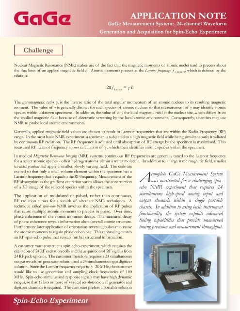
APPLICATION NOTE - Gage Applied Technologies, Inc.
APPLICATION NOTE - Gage Applied Technologies, Inc.
APPLICATION NOTE - Gage Applied Technologies, Inc.

Create successful ePaper yourself
Turn your PDF publications into a flip-book with our unique Google optimized e-Paper software.
fand must control the system from the within the C and MATLAB Windows programming environments.In addition to the basic generator and digitizer requirements, the customer requires extreme timing accuracy and stability. Firstly, allgenerator and digitizer channels must operate using a common master conversion clocking signal that has an absolute accuracy ofbetter than 1 part-per-million. Secondly, the customer must position digitizer sampling clock edges with 1 nanosecond resolutionwithin the spin-echo response signals, which typically occur 20 milliseconds after the excitation pulses.SolutionIntegrated Portable GaGe Measurement SystemThrough direct consultation with the customer, GaGe application engineers prepared a complete GaGe Measurement System tosolve the requirement. Consisting entirely of standard GaGe catalog products and functionalities, the system is equipped withseven GaGe PCI instrument cards:• Three Octopus CompuScope 8389 digitizers (8 channels, 14-bits, 125 MS/s max)• Three CompuGen 8152 waveform generators (8 channels, 12-bits, 150 MS/s max)• CompuGen 11G2 waveform generators (1 channel, 12-bits, 1 GS/s max)All instrument cards are housed within a GaGe Instrument Mainframe 7500 portable lunchbox computer. A photographof the system is shown on Page 1.Figure 1 shows the electrical connectors for all GaGe PCI instrument cards, which are accessed through a PCI back-plate panelon the left hand side of the system. For convenience and slot economy, the auxiliary timing connections for the three CG8152cards (Trigger In, Clock In and Marker Out) havebeen combined on a single auxiliary connectorback-plate. In addition to the usual PCI backplateretaining screw, all cards are secured withinthe chassis by back-end retention bracketing,which improves vibration resistance.The main performance features of the GaGePCI instrument cards meet the requirementof the customer’s application. Each OctopusCompuScope 8389 provides 8 simultaneousinput channels at up to 125 MS/s sampling onall channels with 128 MegaSamples of on-boardacquisition memory. The CS8389 acquires with14 bits of vertical resolution and an impressiveSignal-to-Noise Ratio (SNR) of 66 dB. The threeCS8389s operate together as a 24 input multi-Octopus system, as discussed below.CG8152AuxiliaryConnectionsThree CG8152GeneratorsCG11G2GeneratorThree CS8389DigitizersP S I S IIThe CompuGen 8152 provides 8 simultaneousoutput channels at up to a 150 MHz clockingspeed on all channels with 2 MegaSamples ofwaveform memory behind each channel. TheCG8152 provides 12 bits of vertical resolution andFigure 1: Photo of connections to GaGe PCI instrument cards within the GaGeMeasurement System. Multi-card jumper cables connected between adjacentOctopus CS8389 cards assign them the functional identities of Primary, SecondaryI and Secondary II (from left to right).www.gage-applied.com/applications
<strong>APPLICATION</strong> <strong>NOTE</strong>may drive 50 Ohm loads on each output channel. The customer requires three CG8152s, which will be operated togetherto create a 24 output channel generation system.Multi-card Octopus CompuScope operationEach Octopus CompuScope 8389 is equipped with 8 separate simultaneous input channels. Multiple Octopus CompuScopes mayoperate together with correct cabling of their auxiliary timing connections so that systems with up to 64 simultaneous channelswithin a single chassis may be assembled.Each Octopus CompuScope is equipped with four standard auxiliary timing connections:1. Trigger In: Accepts an external trigger signal.2. Trigger Out: Produces a synchronous digital output pulse whenever the CompuScope triggers3. Clock In: Accepts an external clocking signal.4. Clock Out: Produces an output version of the CompuScope sampling clock signal.For creation of a Multi-Octopus system, one Octopus CompuScope card is selected as the Primary CompuScope . Next, the TriggerOut and Clock Out signals from the Primary CompuScope are respectively connected to the Trigger In and Clock In connectors ofthe neighbouring CompuScope, which is designated as Secondary I. The same connections are made between Secondary I and thelast CompuScope, designated as Secondary II. This cascaded trigger/clock cabling scheme may be repeated for many SecondaryCompuScopes, even if they reside in a separate chassis. Figure 1 shows the customer’s three-card multi-Octopus system connectedby CompuScope jumper cables.The Primary Octopus CompuScope is the Master trigger and clocking source for the multi-Octopus system. All SecondaryCompuScopes are configured in External Clocking and External Triggering Mode. In this way, all cards within the system usethe same trigger and clocking signal, supplied by the Primary, so that all 24 channels sample and trigger together.Small, fixed inter-card propagation delays are introduced by the cascaded clocking and triggering scheme. These delays betweenadjacent Octopus cards may be empirically measured by introducing a simultaneous pulse to all cards. The measurement servesas a calibration, which is then used to time-align waveforms for future waveform acquisitions. Indeed, in many applications,different input signals already suffer differential inter-channel delays, due to differential signal propagation delays in cabling andsensor circuitry. The important thing is that cascading of the clock signal ensures synchronous sampling on all channels, as willbe demonstrated below.The only precaution required when operating an Octopus multi-card system is that all Secondary cards must be armed toawait a trigger before the Primary. Otherwise, a trigger event might occur on the Primary before the Secondaries are armed.Respecting this condition is easy in most applications and this customer will simply generate CompuGen waveforms only afterall CompuScopes are armed.10 MHz reference Signal for High Timing AccuracyWhile the GaGe instrument hardware meets all basic instrumentation requirements, the devil of this experiment is in the highaccuracy timing requirements. Larmor frequencies in the experiment are extremely precise and require instrument timing accuraciesand stabilities that are better than 1 part-per-million (PPM). A 1 PPM 10 MHz reference signal on-board the Octopus CS8389and its accompanying Phase Lock Loop (PLL) circuitry ensure, for instance, that the 125 MHz maximum sampling frequency isexactly 12.5 times the 10 MHz reference frequency. The Octopus CompuScope may be configured to output its 10 MHz referencesignal, which may then be used to synchronize timing on other devices – including another CompuScope cards.www.gage-applied.com/applications
The user may choose to provide an external high-accuracy 10 MHz reference signal to the CompuScope, so that global samplingaccuracy is further improved. Some laboratory facilities are equipped with accurate 10 MHz reference signals that are used byall local experiments. Alternately, 10 MHz reference signals with accuracies a in excess of 50 parts-per-billion may be obtainedfrom IRIG-B devices, which receive accurate timing signals from GPS satellites. The customer has selected the best availableoption and will use an atomic rubidium frequency standard whose 10 MHz reference frequency is accurate to better than 1 partper-billion.Set-up for Testing of Complete SystemTesting of the GaGe Measurement System was accomplished using only GaGe stand-alone Windows application software:CGTest for all CompuGen hardware and <strong>Gage</strong>Scope Professional, the World’s Most Powerful Oscilloscope software, for allCompuScope hardware.The cabling configuration for system testing is shown in Figure 2. At the beginning of the timing signal sequence is a 10 MHzreference signal, which serves as the master timing reference for all instruments. For highest timing accuracy, the customer willuse a 10 MHz reference signal from a rubidium frequency standard. For portable measurements, the customer will use the 10MHz reference from one of the Octopus cards, which provides accuracy of 1 PPM.The CompuGen 11G2 generates its waveform using a 1 GHz clocking signal synchronized to the 10 MHz reference signal. TheCG11G2 phase-locking reference circuitry ensuresthat its 1 GHz clocking frequency is exactly 100times the 10 MHz reference frequency. For testing,the CG11G2 was loaded with a repeating patternof four HIGH samples, followed by four LOWsamples. This pattern is seamlessly looped togenerate a continuous 125 MHz clocking signal thatis exactly 12.5 times the 10 MHz master referencefrequency.A small 16 dB in-line amplifier buffers theCG11G2’s 125 MHz output signal, after whichit is connected to a 1-to-4 RF splitter unit. Asshown in Figure 2, one output of the RF splitteris connected to the Clock In input of the PrimaryCS8389, which then passes the clocking signal toall Secondaries. The remaining three RF outputsare connected to the Clock In inputs of the threeCG8152s. Operation in External Clocking modeensures that all CG8152s and CS8389s use thecommon 125 MHz conversion clocking signal.The three CG8152 cards are configured so thatthey trigger together in a cascaded fashion. Patterngeneration from the CG8152 #1 (as identified inFig 2) is triggered externally by a function generator.Positioned at the beginning of the pattern fromCG8152 #1 is a digital Marker Out pulse, whichexternally triggers CG8152 #2. Similarly, a MarkerOut pulse from CG8152 #2 externally triggersCI1TI1MRK1CI2TI2MRK2CI3TI3MRK3CG8152AUXFUNCTIONGENERATOR12345678CG81521-to-4 RFSPLITTER10 MHzREFERENCESIGNAL12345678CG815212345678CG8152CITICG11G2CG8152 #1 CG8152 #2 CG8152 #3 MasterClockGenerator16 dBOUTMRKR2468TITO1357CICOCS83892468TITO1357CICOCS83892468TITO1357CICOCS8389Primary Secondary I Secondary IIFigure 2: Cabling configuration used for testing of <strong>Gage</strong> Measurement System. Forclarity, cables are illustrated as transparent and connections between the 24 CompuGenoutput channels and the 24 Octopus CompuScope input channels are not shown.The following abbreviations are used: TI for Trigger In, TO for Trigger Out, CI forClock In, CO for Clock Out and MRKR for CompuGen Marker Out.www.gage-applied.com/applications
CG8152 #3. The user may compensate for slight inter-CompuGen delays by appropriately shifting each Marker pulse and/orpattern position in time. Finally, a Marker Out pulse from CG8152 #3 externally triggers the Primary CS8389, which then triggersall Secondary CompuScopes in the multi-Octopus system.ResultsFigure 3 shows a an image of the system during testing under <strong>Gage</strong>Scope, which operates all CompuScope hardware. Separatedisplays for the three CompuScope 8389 cards are shown in their functional order (from left to right, Primary, Secondary I andSecondary II).Figure 3: Image of <strong>Gage</strong>Scope Professional operating the system during testing. TheCompuGen 8152 waveforms acquired by each of the three 8-channel Octopus CS8389cards are shown in three separate displays.As discussed, all CS8389s are externally clockedby the same 125 MHz clocking signal createdby the CG11G2. Clocking and TriggeringSignals are cascaded throughout the threecardmulti-Octopus by the multi-Octopusjumper cables. For testing, a sine wave pulsewas generated upon half of the twenty-fourCG8152 channels. Figure 3 shows that allmulti-Octopus input channels acquire thesame sine pulse with the same amplitude andposition. Consequently, Figure 3 providesbasic validation that the multi-Octopus systemoperates correctly.More powerful validation of the system isshown in Figure 4, where only cosmetic<strong>Gage</strong>Scope display settings have been changedfrom Figure 3. The horizontal and vertical scales are magnified. In addition, <strong>Gage</strong>Scope Persistence mode ensures that displayscreens are not erased between successive waveform acquisitions. Persistence mode allows direct measurement of signal jitter,which is equal to the width in time of the ribbon-like waveform lines of Figure 4.By definition, asynchronous waveform acquisitionmeans that acquired waveforms and thedigitizer sampling clock are not correlated inany way. Asynchronous acquisition alwaysleads to a signal jitter of one samplinginterval, which is 4 nanoseconds at the 125MS/s sampling rate. This one-point jitter isno failing of the CompuScope hardware butis a fundamental consequence of signal andsampling clock asynchronicity.When the sampling clock and acquiredwaveform are synchronous, waveform triggersalways occurs at the same phase of thesampling clock. In this case, waveformstability becomes limited only by the intrinsicelectrical jitter of the CompuScope hardwareFigure 4: <strong>Gage</strong>Scope image taken under the conditions of Figure 3 with changesonly to cosmetic display settings. Both the time-base and horizontal scale settings aremagnified. Persistence or Overdraw Mode, which suppresses the erasure of successivewaveforms, is also active.www.gage-applied.com/applications
components. The magnified view of Figure 4 shows that waveform jitter on all channels of the multi-Octopus system is wellbelow the 4 nanosecond sampling interval. Indeed, the residual jitter is below 1 nanosecond and more likely results from slightnoise on the signals, rather than from intrinsic timing jitter. Consequently, Figure 4 clearly establishes the clock synchronicity ofthe entire system that results from the common 125 MHz clocking signal.CompuScope Software Development KitsUltimately, the customer will create a tailored software application using GaGe’s powerful CompuScope C/C# and MATLABSoftware Development Kits (SDKs). In addition to allowing full hardware control, SDKs also provide access to advancedCompuScope functionality that is not available under <strong>Gage</strong>Scope. For example, the customer’s short spin-echo response pulsestypically occur 20 milliseconds after the CompuGen excitation pulses, which trigger the CompuScope hardware. Simple acquisitionunder <strong>Gage</strong>Scope, therefore, would waste CompuScope memory by acquiring over 2 million samples in order to extract only thefew thousand trailing samples of interest.From any CompuScope SDK, the user may activate the CompuScope Trigger Delay feature, which simply delays the CompuScopetrigger by a programmable number of sample points. In the customer’s case, a Trigger Delay value of 2,000,000 points at 100MS/s delays triggering until occurrence of the few thousand points of interest. Using the Trigger Delay feature from an SDK,therefore, the customer is able to expend only the minimum required amount of on-board memory.Multiple Record ModeThe customer will use Multiple Record Mode to rapidly acquire sequential waveforms, which are stacked in on-board memory. Forexample, in Multiple Record Mode, 8000 waveforms of 2000 Samples each may be acquired into the CS8389’s 128 MegaSamples(16 MS/channel) memory.Between sequential acquisitions in Multiple Record mode, trigger circuitry is re-armed in hardware with no software interventionrequired. Software intervention is accompanied by software latencies of indeterminate length, which may lead to trigger loss inan unpredictable fashion. By contrast, hardware re-arming in Multiple Record Mode is completely deterministic and requires nomore than 2 microseconds at the smallest waveform lengths. For waveform lengths longer than 16,000 Samples, the hardwarere-arm time drops below 0.5 microseconds.Stored with each Multiple Record waveform trigger is a Trigger Time-Stamp value that is derived from a 44-bit on-board counteroutput, which is latched upon each trigger event. The counter may be clocked by the CompuScope sampling clock or by a fixed133 MHz on-board oscillator. Trigger Time Stamps, therefore, allow measurement of each trigger event’s occurrence time withan accuracy of better than 10 nanoseconds.CompuGen Link’N’Loop FunctionalityThe customer’s NMR Larmor frequencies are accurate to better than 1 part-per million and CompuScope sampling clock edgesmust be positioned with a precision of 1 nanosecond – even after a 20 millisecond spin-echo delay. In the simplest approach,clock edge positions might be adjusted within 1 nanosecond by appropriately modifying the 100 MHz clocking signal loaded asCG11G2 pattern. The 16 MegaSamples of CG11G2 memory at a clocking speed of 1 GHz, however, only allows for a maximumarbitrary pattern duration of 16 milliseconds, which is below the 20 millisecond requirement.Fortunately, because the customer’s clocking signal is mostly repetitive, the requirement may exploit CompuGen Link’N’Loopmode. Somewhat similar to CompuScope Multiple Record Mode, Link’N’Loop mode allows a portfolio of waveform patternsto be pre-loaded to CompuGen memory. After loading, the user may rapidly switch amongst the waveform portfolio with adeterministic 64 point pattern switching time. Each waveform may be seamlessly looped for an adjustable loop count.The customer’s requirement is satisfied through the creation of three Link’N’Loop waveform segments that are illustrated inFigure 5. The first Link’N’Loop segment contains all 0 values but also generates a Marker Out Pulse that triggers CG8152 #1,
which, in turn, ultimately triggers all other instrument cards.The second Link’N’Loop segment is a “coarse” repetitive 100 MHz clocking signal. For example, let us assume that Segment#2 is exactly 6,400 samples long and contains exactly 640 clock pulses of 10 samples each. If it operates at a 1 GHz clockingrate and seamlessly loops Segment #2 exactly 3125 times, the CG11G2 will create a continuous 100 MHz clocking signal for aduration of exactly 6,400 x 3125 / 1 GHz = 20 milliseconds. The user may lengthen or shorten the duration of Segment #2 in6.4 microsecond increments, simply by increasing or decreasing the 3125 loop count.Once Segment #2 has completed, Segment #3 serves asa single-shot “Footer” clocking pattern, whose clockingedges may be placed precisely with 1 nanosecondresolution simply by shifting the entire pattern left orright. The length of Segment #3 is only a few thousand100 MHz clock cycles, as required to complete theCompuScope spin-echo response signal acquisition.There are two constant 64-sample segment switchingdelays within the CG11G2 Link’N’Loop generationsequence, in addition to other constant propagationdelays. The user must compensate for these delays forcorrect clocking edge positioning. This is most easilydone once by trial-and–error.MarkerSegment#1SwitchCoarse LongSegment #2Seamless Looping of Segment #2SwitchFooter Segment #3The overall 3-segment Link’N’Loop pattern may beendlessly looped by the CG11G2 or generated onceupon its receipt of an external trigger pulse. By usingCompuGen Link’N’Loop mode, therefore, the customeris able to reduce the raw CG11G2 memory lengthrequirement from an unavailable 20 MegaSamples toonly a few tens of thousands of samples.Endless Looping of Overall Link’N’Loop sequenceFigure 5: The diagram shows the three waveform segments in CompuGenLink’N’Loop mode that are required to create the user’s precision 100 MHzclocking signal.ConclusionA complete portable 24 channel high-speed analog input/output GaGe Measurement System was constructed for a demandingspin-echo NMR using only CompuGen and CompuScope PCI instrument cards from the GaGe catalog. A high-speed CompuGenCG11G2 generator card was used to create a high accuracy, synchronous Master clocking signal for by all GaGe instruments.Almost all functionality required for the application is available under GaGe’s powerful stand-alone application software: CGTestand <strong>Gage</strong>Scope. These functionalities include:• Loading of independent arbitrary waveforms onto all four CompuGen cards.• Simultaneous operation of all three CompuScope cards• Creation of a 125 MHz Master clocking signal with the CompuGen 11G2• Operation of a multi-Octopus system with jumper cables supplied
• Operation with cabling configuration for common clocking and triggering of all instrument cards• Usage of a Master 10 MHz reference signal to provide high accuracy timing on all instrumentsResultsMore advanced functionalities that are accessible from GaGe Software Development Kits include:Drivers• UsageforofboththeWindowsCompuScope95 andTriggerWindowsDelayNTfeatureare availableto minimizefor theCompuScopeCS8500.memory usage in Multiple Record ModeIn addition, <strong>Gage</strong>Scope software will allow the customer to do exactly whatthey • Usage asked: of verify CompuGen the operation Link’N’Loop of the Mode CompuScope to allow nanosecond 8500/PCI positioning without of CG11G2 clocking edges long after the startwriting of generation. any code.Knowing the powerful GaGe PCI instrument portfolio and understanding their basic and advanced functionality, GaGe applicationengineers were able to recommend a GaGe Measurement System that completely fulfills this challenging requirement.Octopus CompuScope Family<strong>Gage</strong>’s Octopus family of multi-channel digitizers features up to 8channels, up to 4 GB of on-board acquisition memory, and up to 125 MS/ssampling per channel on a single-slot PCI card.Features• 2, 4, or 8 digitizing channels• 12 bit or 14 bit vertical resolution• 128 MS to 2 GS on-board acquisitionmemory• 10, 25, 50, 65, 100, or 125 MS/s maximumsampling per channel• More than 100 MHz input analog bandwidth• Full-featured front-end, with software control over input ranges,coupling and terminating impedance• 32 bits, 66 MHz PCI standard for 200 MB/s data transfer to PCmemory• Ease of integration with External or Reference Clock In and ClockOut, External Trigger In and Trigger Out• eXpert on-board processing FPGA firmware available for SignalAveraging, FIR filtering and Peak Detection• Programming-free operation with <strong>Gage</strong>Scope® oscilloscope software• Software Development Kits available for LabVIEW, MATLAB, C/C#This application brief is provided “as is” without any warranties of any kind,either expressed or implied, including but not limited to the implied warranties ofGaGe does not warrant the accuracy andcompleteness of the material contained herein.GaGe may make changes to this material, or to theproducts described in it, at any time without notice.Copyright 900 N. © 2005 State <strong>Gage</strong> Street <strong>Applied</strong> • Lockport, <strong>Technologies</strong>. IL 60441 All rights • 1-800-567-GaGe reserved. • Phone: +1-514-633-7447 • Fax: +1-514-633-0770 • prodinfo@gage-applied.comwww.gage-applied.com/applications