ML13135_rev0 - LANSDALE Semiconductor Inc.
ML13135_rev0 - LANSDALE Semiconductor Inc.
ML13135_rev0 - LANSDALE Semiconductor Inc.

You also want an ePaper? Increase the reach of your titles
YUMPU automatically turns print PDFs into web optimized ePapers that Google loves.
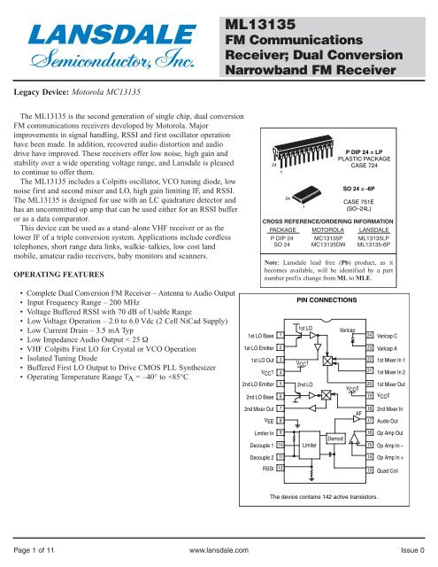
<strong>ML13135</strong><br />
FM Communications<br />
Receiver; Dual Conversion<br />
Narrowband FM Receiver<br />
Legacy Device: Motorola MC13135<br />
The <strong>ML13135</strong> is the second generation of single chip, dual conversion<br />
FM communications receivers developed by Motorola. Major<br />
improvements in signal handling, RSSI and first oscillator operation<br />
have been made. In addition, recovered audio distortion and audio<br />
drive have improved. These receivers offer low noise, high gain and<br />
stability over a wide operating voltage range, and Lansdale is pleased<br />
to continue to offer them.<br />
The <strong>ML13135</strong> includes a Colpitts oscillator, VCO tuning diode, low<br />
noise first and second mixer and LO, high gain limiting IF, and RSSI.<br />
The <strong>ML13135</strong> is designed for use with an LC quadrature detector and<br />
has an uncommitted op amp that can be used either for an RSSI buffer<br />
or as a data comparator.<br />
This device can be used as a stand–alone VHF receiver or as the<br />
lower IF of a triple conversion system. Applications include cordless<br />
telephones, short range data links, walkie–talkies, low cost land<br />
mobile, amateur radio receivers, baby monitors and scanners.<br />
OPERATING FEATURES<br />
24<br />
1<br />
24<br />
1<br />
P DIP 24 = LP<br />
PLASTIC PACKAGE<br />
CASE 724<br />
SO 24 = -6P<br />
CASE 751E<br />
(SO–24L)<br />
CROSS REFERENCE/ORDERING INFORMATION<br />
PACKAGE<br />
MOTOROLA<br />
<strong>LANSDALE</strong><br />
P DIP 24 MC13135P <strong>ML13135</strong>LP<br />
SO 24 MC13135DW <strong>ML13135</strong>-6P<br />
Note: Lansdale lead free (Pb) product, as it<br />
becomes available, will be identified by a part<br />
number prefix change from ML to MLE.<br />
• Complete Dual Conversion FM Receiver – Antenna to Audio Output<br />
• Input Frequency Range – 200 MHz<br />
• Voltage Buffered RSSI with 70 dB of Usable Range<br />
• Low Voltage Operation – 2.0 to 6.0 Vdc (2 Cell NiCad Supply)<br />
• Low Current Drain – 3.5 mA Typ<br />
• Low Impedance Audio Output < 25 Ω<br />
• VHF Colpitts First LO for Crystal or VCO Operation<br />
• Isolated Tuning Diode<br />
• Buffered First LO Output to Drive CMOS PLL Synthesizer<br />
• Operating Temperature Range TA = –40° to +85°C<br />
1st LO Base<br />
1st LO Emitter<br />
1st LO Out<br />
VCC1<br />
2nd LO Emitter<br />
2nd LO Base<br />
PIN CONNECTIONS<br />
1st LO<br />
Varicap<br />
1 24<br />
2<br />
23<br />
3<br />
22<br />
VCC1<br />
4<br />
21<br />
5 2nd LO<br />
20<br />
VCC2<br />
6<br />
19<br />
Varicap C<br />
Varicap A<br />
1st Mixer In 1<br />
1st Mixer In 2<br />
1st Mixer Out<br />
VCC2<br />
2nd Mixer Out<br />
VEE<br />
7<br />
8<br />
AF<br />
18<br />
17<br />
2nd Mixer In<br />
Audio Out<br />
Limiter In<br />
Decouple 1<br />
9<br />
10<br />
Limiter<br />
Demod<br />
16<br />
15<br />
Op Amp Out<br />
Op Amp In –<br />
Decouple 2<br />
11<br />
14<br />
Op Amp In +<br />
RSSI<br />
12<br />
13<br />
Quad Coil<br />
The device contains 142 active transistors.<br />
Page 1 of 11 www.lansdale.com<br />
Issue 0
<strong>ML13135</strong><br />
<strong>LANSDALE</strong> <strong>Semiconductor</strong>, <strong>Inc</strong>.<br />
MAXIMUM RATINGS<br />
Rating Pin Symbol Value Unit<br />
Power Supply Voltage 4, 19 VCC (max) 6.5 Vdc<br />
RF Input Voltage 22 RFin 1.0 Vrms<br />
Junction Temperature – TJ +150 °C<br />
Storage Temperature Range – Tstg – 65 to +150 °C<br />
RECOMMENDED OPERATING CONDITIONS<br />
Rating Pin Symbol Value Unit<br />
Power Supply Voltage 4, 19 VCC 2.0 to 6.0 Vdc<br />
Maximum 1st IF – fIF1 21 MHz<br />
Maximum 2nd IF – fIF2 3.0 MHz<br />
Ambient Temperature Range – TA – 40 to + 85 °C<br />
ELECTRICAL CHARACTERISTICS (TA = 25°C, VCC = 4.0 Vdc, fo = 49.7 MHz, fMOD = 1.0 kHz, Deviation = ±3.0 kHz, f1stLO = 39 MHz, f2nd<br />
LO = 10.245 MHz, IF1 = 10.7 MHz, IF2 = 455 kHz, unless otherwise noted. All measurements performed in the test circuit of Figure 1.)<br />
Characteristic Condition Symbol Min Typ Max Unit<br />
Total Drain Current No Input Signal ICC – 4.0 6.0 mAdc<br />
Sensitivity (Input for 12 dB SINAD) Matched Input VSIN – 1.0 – µVrms<br />
Recovered Audio VRF = 1.0 mV AFO 170 220 300 mVrms<br />
1st Mixer Conversion Gain VRF = – 40 dBm MXgain1 – 12 – dB<br />
2nd Mixer Conversion Gain VRF = – 40 dBm MXgain2 – 13 – dB<br />
First LO Buffered Output – VLO – 100 – mVrms<br />
Total Harmonic Distortion VRF = – 30 dBm THD – 1.2 3.0 %<br />
Demodulator Bandwidth – BW – 50 – kHz<br />
RSSI Dynamic Range – RSSI – 70 – dB<br />
First Mixer 3rd Order Intercept TOIMix1 dBm<br />
(Input) Matched – –17 –<br />
Unmatched – –11 –<br />
Second Mixer 3rd Order Matched TOIMix2 dBm<br />
Intercept (RF Input) Input – – 27 –<br />
First LO Buffer Output Resistance – RLO – – – Ω<br />
First Mixer Parallel Input Resistance – R – 722 – Ω<br />
First Mixer Parallel Input Capacitance – C – 3.3 – pF<br />
First Mixer Output Impedance – ZO – 330 – Ω<br />
Second Mixer Input Impedance – ZI – 4.0 – kΩ<br />
Second Mixer Output Impedance – ZO – 1.8 – kΩ<br />
Detector Output Impedance – ZO – 25 – Ω<br />
Page 2 of 11 www.lansdale.com<br />
Issue 0
<strong>ML13135</strong><br />
<strong>LANSDALE</strong> <strong>Semiconductor</strong>, <strong>Inc</strong>.<br />
TEST CIRCUIT INFORMATION<br />
The recovered audio measurements for the <strong>ML13135</strong> are<br />
made with an LC quadrature detector. The typical recovered<br />
audio will depend on the external circuit; either the Q of the<br />
quad coil, or the RC matching network for the ceramic discriminator.<br />
See Figures 10 and 11 for additional information.<br />
Since adding a matching circuit to the RF input increases the<br />
signal level to the mixer, the third order intercept (TOI) point<br />
is better with an unmatched input (50 Ω from Pin 21 to Pin<br />
22). Typical values for both have been included in the<br />
Electrical Characterization Table. TOI measurements were<br />
taken at the pins with a high impedance probe/spectrum analyzer<br />
system. The first mixer input impedance was measured at<br />
the pin with a network analyzer.<br />
Figure 1a. <strong>ML13135</strong> Test Circuit<br />
VCC<br />
0.1<br />
1.0 k<br />
0.1<br />
0.84 µH<br />
39.0<br />
MHz<br />
Xtal<br />
5.0 k<br />
120 p<br />
0.01<br />
20 p<br />
5.0 p<br />
50 p<br />
1<br />
2<br />
3<br />
4<br />
5<br />
6<br />
1st LO<br />
VCC1<br />
2nd LO<br />
Varicap<br />
VCC2<br />
24<br />
23<br />
22<br />
21<br />
20<br />
19<br />
0.001<br />
0.2 µH<br />
0.01<br />
Ceramic<br />
Filter<br />
10.7 MHz<br />
Figure 1.<br />
62 pF<br />
180 p<br />
RF<br />
Input<br />
10.245<br />
MHz Xtal<br />
Ceramic<br />
Filter<br />
455 kHz<br />
0.1<br />
0.1<br />
0.1<br />
7<br />
8<br />
9<br />
10<br />
11<br />
Limiter<br />
Demod<br />
AF<br />
18<br />
17<br />
16<br />
15<br />
8.2 k<br />
0.1<br />
0.1<br />
360<br />
39 k<br />
12<br />
14<br />
0.1<br />
13<br />
39 k<br />
455 kHz<br />
Quad<br />
Coil<br />
Page 3 of 11 www.lansdale.com<br />
Issue 0
<strong>ML13135</strong><br />
<strong>LANSDALE</strong> <strong>Semiconductor</strong>, <strong>Inc</strong>.<br />
Figure 2. Supply Current versus Supply Voltage<br />
6.0<br />
1400<br />
Figure 3. RSSI Output versus RF Input<br />
I C C , SUPPLY CURRENT (mA )<br />
5.0<br />
4.0<br />
3.0<br />
2.0<br />
1.0<br />
RFin = 49.7 MHz<br />
fMOD = 1.0 kHz<br />
fDEV = ± 3.0 kHz<br />
RSSI OUTPUT (mVdc, Pin 12)<br />
1200<br />
1000<br />
800<br />
600<br />
400<br />
VCC = 4.0 V<br />
RFin = 49.67 MHz<br />
fMOD = 1.0 kHz<br />
fDEV = ± 3.0 kHz<br />
0<br />
0<br />
1.0 2.0 3.0 4.0 5.0 6.0 7.0 8.0<br />
VCC, SUPPLY VOLTAGE (V)<br />
200<br />
–140<br />
–120 –100 – 80 – 60 – 40 – 20<br />
RF INPUT (dBm)<br />
C P , EQUIVALENT PARALLEL CAPACITANCE (pF )<br />
25<br />
20<br />
15<br />
10<br />
5.0<br />
0<br />
0.5<br />
Figure 4. Varactor Capacitance, Resistance<br />
versus Bias Voltage<br />
CP, f = 150 MHz<br />
CP, f = 50 MHz<br />
RP, f = 50 MHz<br />
RP, f = 150 MHz<br />
0<br />
1.0 1.5 2.0 2.5 3.0 3.5 4.0<br />
VB, VARACTOR BIAS VOLTAGE, VPin24 to VPin 23 (Vdc)<br />
10<br />
8.0<br />
6.0<br />
4.0<br />
2.0<br />
R P , EQUIVALENT PARALLEL RESISTANCE (k Ω )<br />
f, FREQUENCY (MHz)<br />
48.0<br />
47.5<br />
47.0<br />
46.5<br />
46.0<br />
45.5<br />
45.0<br />
1.0<br />
Figure 5. Oscillator Frequency<br />
versus Varactor Bias<br />
500 p<br />
27 p<br />
5.0 p<br />
1<br />
2<br />
1st LO<br />
Varicap<br />
2.0 3.0 4.0 5.0 6.0<br />
VB, VARACTOR BIAS VOLTAGE (Vdc)<br />
24<br />
23<br />
0.61 µH<br />
500 p<br />
1.0 MΩ 0.2 µF<br />
V B<br />
POWER (dBm)<br />
Figure 6. Signal Levels versus RF Input<br />
30<br />
10<br />
Second Mixer Output<br />
–10<br />
–30<br />
First Mixer Output<br />
First Mixer Input<br />
–50<br />
Second Mixer Input<br />
– 70<br />
–100 – 90 – 80 – 70 – 60 – 50 – 40 – 30 – 20<br />
RFin, RF INPUT (dBm)<br />
S+N, N, AND AMR (dB)<br />
10<br />
0<br />
–10<br />
– 20<br />
– 30<br />
– 40<br />
– 50<br />
– 60<br />
– 70<br />
–130<br />
Figure 7. Signal + Noise, Noise, and<br />
AM Rejection versus Input Power<br />
VCC = 4.0 Vdc<br />
RFin = 49.67 MHz<br />
fMOD = 1.0 kHz<br />
fDEV = ± 3.0 kHz<br />
–110 – 90 – 70 – 50 – 30<br />
RFin, RF INPUT (dBm)<br />
S + N<br />
S + N 30% AM<br />
N<br />
Page 4 of 11 www.lansdale.com<br />
Issue 0
<strong>ML13135</strong><br />
<strong>LANSDALE</strong> <strong>Semiconductor</strong>, <strong>Inc</strong>.<br />
50<br />
Figure 8. Op Amp Gain and Phase<br />
versus Frequency<br />
80<br />
Figure 9. First Mixer Third Order Intermodulation<br />
(Unmatched Input)<br />
20<br />
A V , GAIN (dB )<br />
30<br />
10<br />
0<br />
–10<br />
– 30<br />
Gain<br />
Phase<br />
120<br />
160<br />
200<br />
240<br />
,φ EXCESS PHASE (DEGREES)<br />
MIXER OUTPUT (dB)<br />
0<br />
– 20<br />
– 40<br />
– 60<br />
– 80<br />
Desired Products<br />
3rd Order<br />
Intermod<br />
Products<br />
– 50<br />
10 k<br />
100 k 1.0 M 10 M<br />
f, FREQUENCY (Hz)<br />
280<br />
–100<br />
–100<br />
– 80 – 60 – 40 – 20 0<br />
RF INPUT (dBm)<br />
pp<br />
)<br />
RA, RECOVERED AUDIO (mV<br />
2000<br />
1500<br />
1000<br />
500<br />
0<br />
±1.0<br />
13<br />
Figure 10. Recovered Audio versus<br />
Deviation for <strong>ML13135</strong><br />
R<br />
VCC<br />
455 kHz<br />
Quad Coil<br />
Toko 7MC–8128Z<br />
fDEV, DEVIATION (kHz)<br />
R = 68 kΩ<br />
R = 47 kΩ<br />
R = 39 kΩ<br />
± 3.0 ± 5.0 ± 7.0 ± 9.0<br />
TOTAL HARMONIC DISTORTION (%)<br />
THD,<br />
8.0<br />
7.0<br />
6.0<br />
5.0<br />
4.0<br />
3.0<br />
13<br />
R<br />
Figure 11. Distortion versus<br />
Deviation for <strong>ML13135</strong><br />
VCC<br />
455 kHz<br />
Quad Coil<br />
Toko 7MC–8128Z<br />
2.0<br />
R = 39 kΩ<br />
1.0<br />
±1.0 ± 3.0 ± 5.0 ± 7.0 ± 9.0<br />
fDEV, DEVIATION (kHz)<br />
R = 68 kΩ<br />
R = 47 kΩ<br />
Page 5 of 11 www.lansdale.com<br />
Issue 0
<strong>ML13135</strong><br />
<strong>LANSDALE</strong> <strong>Semiconductor</strong>, <strong>Inc</strong>.<br />
CIRCUIT DESCRIPTION<br />
The <strong>ML13135</strong> is a complete dual conversion receiver. This<br />
includes two local oscillators, two mixers, a limiting IF amplifier<br />
and detector, and an op amp. It will provide a voltage<br />
buffered RSSI with 70 dB of usable range, isolated tuning<br />
diode and buffered LO output for PLL operation, and a separate<br />
VCC pin for the first mixer and LO. Improvements have<br />
been made in the temperature performance of both the recovered<br />
audio and the RSSI.<br />
VCC<br />
Two separate V CC lines enable the first LO and mixer to<br />
continue running while the rest of the circuit is powered down.<br />
They also isolate the RF from the rest of the internal circuit.<br />
Local Oscillators<br />
The local oscillators are grounded collector Colpitts, which<br />
can be easily crystal–controlled or VCO controlled with the<br />
on–board varactor and external PLL. The first LO transistor is<br />
internally biased, but the emitter is pinned–out and IQ can be<br />
increased for high frequency or VCO operation. The collector<br />
is not pinned out, so for crystal operation, the LO is generally<br />
limited to 3rd overtone crystal frequencies; typically around 60<br />
MHz. For higher frequency operation, the LO can be provided<br />
externally as shown in Figure 16.<br />
Buffer<br />
An amplifier on the 1st LO output converts the single–ended<br />
LO output to a differential signal to drive the mixer. Capacitive<br />
coupling between the LO and the amplifier minimizes the<br />
effects of the change in oscillator current on the mixer.<br />
Buffered LO output is pinned–out at Pin 3 for use with a PLL,<br />
with a typical output voltage of 320 mVpp at VCC= 4.0 V and<br />
with a 5.1 k resistor from Pin 3 to ground. As seen in Figure<br />
14, the buffered LO output varies with the supply voltage and<br />
a smaller external resistor may be needed for low voltage operation.<br />
The LO buffer operates up to 60 MHz, typically. Above<br />
60 MHz, the output at Pin 3 rolls off at approximately 6.0 dB<br />
per octave. Since most PLLs require about 200 mVpp drive, an<br />
external amplifier may be required.<br />
Mixers<br />
The first and second mixer are of similar design. Both are<br />
double balanced to suppress the LO and input frequencies to<br />
give only the sum and difference frequencies out. This configuration<br />
typically provides 40 to 60 dB of LO suppression. New<br />
design techniques provide improved mixer linearity and third<br />
order intercept without increased noise. The gain on the output<br />
of the 1st mixer starts to roll off at about 20 MHz, so this<br />
receiver could be used with a 21 MHz first IF. It is designed<br />
for use with a ceramic filter, with an output impedance of 330<br />
Ω. A series resistor can be used to raise the impedance for use<br />
with a crystal filter, which typically has an input impedance of<br />
4.0 kΩ. The second mixer input impedance is approximately<br />
4.0 kΩ; it requires an external 360 Ω parallel resistor for use<br />
with a standard ceramic filter.<br />
Limiting IF Amplifier and Detector<br />
The limiter has approximately 110 dB of gain, which starts<br />
rolling off at 2.0 MHz. Although not designed for wideband<br />
operation, the bandwidth of the audio frequency amplifier has<br />
been widened to 50 kHz, which gives less phase shift and<br />
enables the receiver to run at higher data rates. However, care<br />
should be taken not to exceed the bandwidth allowed by local<br />
regulations.<br />
The <strong>ML13135</strong> is designed for use with an LC quadrature<br />
detector, and does not have sufficient drive to be used with a<br />
ceramic discriminator. The discriminators and the external<br />
matching circuit will affect the distortion and recovered audio.<br />
RSSI/Op Amp<br />
The Received Signal Strength Indicator (RSSI) on the<br />
<strong>ML13135</strong> has about 70 dB of range. The resistor needed to<br />
translate the RSSI current to a voltage output has been included<br />
on the internal circuit, which gives it a tighter tolerance. A<br />
temperature compensated reference current also improves the<br />
RSSI accuracy over temperature. On the <strong>ML13135</strong>, the op amp<br />
is not connected internally and can be used for the RSSI or as<br />
a data slicer (see Figure 17c).<br />
600<br />
Figure 14. Buffered LO Output Voltage<br />
versus Supply Voltage<br />
500<br />
RPin3 = 3.0 kΩ<br />
O UTPUT (mV p p<br />
)<br />
400<br />
300<br />
RPin3 = 5.1 kΩ<br />
200<br />
100<br />
2.5 3.0 3.5 4.0 4.5 5.0 5.5<br />
VCC, SUPPLY VOLTAGE (Vdc)<br />
Page 6 of 11 www.lansdale.com<br />
Issue 0
<strong>ML13135</strong><br />
<strong>LANSDALE</strong> <strong>Semiconductor</strong>, <strong>Inc</strong>.<br />
Figure 15. PLL Controlled Narrowband FM Receiver at 46/49 MHz<br />
VCC<br />
<strong>ML13135</strong><br />
0.1<br />
OSC<br />
Out<br />
OSC<br />
In<br />
VDD Fin1<br />
D0 PD1<br />
D1 PD2<br />
D2 LD<br />
D3<br />
VSS Fin2<br />
ML145168<br />
0.1<br />
2.7 k<br />
47 k<br />
1.0<br />
3.0 p<br />
100 k<br />
0.01<br />
0.68 µH<br />
0.1<br />
10.245<br />
MHz Xtal<br />
Ceramic<br />
Filter<br />
455 kHz<br />
0.1<br />
500 p<br />
120 p<br />
500 p<br />
27 p<br />
5.0 p<br />
5.1 k<br />
0.1<br />
50 p<br />
1<br />
2<br />
3<br />
4<br />
5<br />
6<br />
7<br />
8<br />
9<br />
10<br />
11<br />
1st LO<br />
VCC1<br />
2nd LO<br />
Limiter<br />
Varicap<br />
VCC2<br />
AF<br />
Demod<br />
24<br />
23<br />
22<br />
21<br />
20<br />
19<br />
18<br />
17<br />
16<br />
15<br />
0.001<br />
0.01<br />
1.0 k<br />
0.1<br />
0.15<br />
0.2 µH<br />
Ceramic<br />
Filter<br />
10.7 MHz<br />
360<br />
10 k<br />
62 pF<br />
150 pF<br />
RF<br />
Input<br />
Recovered<br />
Audio<br />
RSSI<br />
Output<br />
12<br />
14<br />
0.1<br />
13<br />
68 k<br />
455 kHz<br />
Quad Coil<br />
Figure 16. 144 MHz Single Channel Application Circuit<br />
1st LO External Oscillator Circuit<br />
Preamp for <strong>ML13135</strong> at 144.455 MHz<br />
0.82 µ<br />
1.0 k<br />
15 k<br />
100 p<br />
5.6 k<br />
X1<br />
68 p<br />
43 p<br />
L1<br />
VCC<br />
Q1<br />
+<br />
1.0 µF<br />
15 p<br />
1000p<br />
fosc =<br />
133.755 MHz<br />
470 Q1 – MPS5179<br />
X1 – 44.585 MHz 3rd Overtone<br />
Series Resonant Crystal<br />
L1 – 0.078 µH Inductor<br />
(Coilcraft Part # 146–02J08)<br />
RF Input<br />
3300 p<br />
470 p<br />
12 p<br />
L2<br />
5.1 k<br />
3300 p<br />
15 k<br />
1.0 µ<br />
L3<br />
Q1<br />
VCC<br />
470<br />
39 p<br />
+<br />
1.0 µF<br />
12 p<br />
To Mixer<br />
Q1 – MPS5179<br />
L2 – 0.05 µH<br />
L3 – 0.07 µH<br />
Page 7 of 11 www.lansdale.com<br />
Issue 0
<strong>ML13135</strong><br />
<strong>LANSDALE</strong> <strong>Semiconductor</strong>, <strong>Inc</strong>.<br />
Legacy Applications Information<br />
Figure 17a. Single Channel Narrowband FM Receiver at 49.7 MHz<br />
Buffered LO<br />
Output<br />
+<br />
1.0<br />
VCC<br />
1.0 k<br />
1.0 µH<br />
0.01<br />
0.1<br />
2200 p<br />
27 p<br />
39 MHz<br />
Xtal 5.0 p<br />
120 p<br />
5.1 k<br />
50 p<br />
1<br />
2<br />
3<br />
4<br />
5<br />
6<br />
1st LO<br />
VCC1<br />
2nd LO<br />
<strong>ML13135</strong><br />
24<br />
Varicap<br />
23<br />
22<br />
21<br />
20<br />
VCC2<br />
19<br />
0.001<br />
0.01<br />
0.2 µH<br />
Ceramic<br />
Filter<br />
10.7 MHz<br />
Figure 17.<br />
62 pF<br />
150 p<br />
RF Input<br />
50 Ω Source<br />
10.245 MHz<br />
Xtal<br />
Ceramic<br />
Filter<br />
455 kHz<br />
0.1 0.1<br />
7<br />
8<br />
9<br />
10<br />
11<br />
12<br />
Limiter<br />
Demod<br />
18<br />
AF<br />
17<br />
16<br />
15<br />
14<br />
1.0 k<br />
0.1<br />
0.15<br />
360<br />
10 k<br />
Recovered<br />
Audio<br />
RSSI<br />
Output<br />
0.1<br />
13<br />
39 k<br />
455 kHz<br />
Quad Coil<br />
Figure 17b. PC Board Component View<br />
5.1k<br />
3<br />
120p<br />
2200p<br />
27p<br />
5p<br />
0.1<br />
10.245 MHz<br />
XT<br />
4<br />
CF<br />
5<br />
50p<br />
455 KHz<br />
39 MHz<br />
XT<br />
1.0 k<br />
2<br />
MC13135<br />
.001<br />
0.01<br />
10.7 MHz<br />
CF<br />
0.1<br />
7<br />
1<br />
62p<br />
150p<br />
360<br />
1.0k<br />
10k<br />
1.0<br />
+<br />
0.15<br />
NOTES: 1. 0.2 µH tunable (unshielded) inductor<br />
2. 39 MHz Series mode resonant<br />
3rd Overtone Crystal<br />
3. 1.5 µH tunable (shielded) inductor<br />
4. 10.245 MHz Fundamental mode crystal,<br />
32 pF load<br />
5. 455 kHz ceramic filter, muRata CFU 455B<br />
or equivalent<br />
6. Quadrature coil, Toko 7MC–8128Z (7mm)<br />
or Toko RMC–2A6597HM (10mm)<br />
7. 10.7 MHz ceramic filter, muRata SFE10.7MJ–A<br />
or equivalent<br />
0.01<br />
0.1 0.1<br />
0.1<br />
0.22<br />
10<br />
+<br />
+4.7<br />
39K<br />
51K<br />
10k<br />
MC34119<br />
+10<br />
Figure 17c. Optional Data Slicer Circuit<br />
(Using Internal Op Amp)<br />
0.1<br />
6<br />
VCC<br />
Vin<br />
(Pin 17)<br />
20 k 20 k<br />
15<br />
14<br />
0.001 10 k<br />
16<br />
10 k<br />
FSK Data<br />
Output<br />
1.0 M<br />
Page 8 of 11 www.lansdale.com<br />
Issue 0
<strong>ML13135</strong><br />
<strong>LANSDALE</strong> <strong>Semiconductor</strong>, <strong>Inc</strong>.<br />
Legacy Applications Information<br />
Figure 18. PC Board Solder Side View<br />
RF IN<br />
L.O.<br />
A UDIO<br />
V CC<br />
GROUN D<br />
3 .25 ″<br />
SPEAKER<br />
VCC2<br />
RSSI<br />
MC13135<br />
MC13136<br />
3.375″<br />
(Circuit Side View)<br />
Figure 19. PC Board Component View<br />
5.1k<br />
3<br />
120p<br />
2200p<br />
27p<br />
5p<br />
0.1<br />
10.245 MHz<br />
XT<br />
4<br />
CF<br />
5<br />
50p<br />
455 KHz<br />
39 MHz<br />
XT<br />
1.0 k<br />
2<br />
MC13136<br />
.001<br />
0.01<br />
10.7 MHz<br />
CF<br />
0.1<br />
7<br />
1<br />
62p<br />
360<br />
10k<br />
150p<br />
1.0k<br />
1.0<br />
+<br />
0.15<br />
NOTES: 1. 0.2 µH tunable (unshielded) inductor<br />
2. 39 MHz Series mode resonant<br />
3rd Overtone Crystal<br />
3. 1.5 µH tunable (shielded) inductor<br />
4. 10.245 MHz Fundamental mode crystal,<br />
32 pF load<br />
5. 455 kHz ceramic filter, muRata CFU 455B<br />
or equivalent<br />
6. Ceramic discriminator, muRata CDB455C34<br />
or equivalent<br />
7. 10.7 MHz ceramic filter, muRata SFE10.7MJ–A<br />
or equivalent<br />
0.01<br />
0.1 0.1<br />
0.1<br />
270p<br />
0.22<br />
10<br />
+<br />
+4.7<br />
2.7k<br />
10k<br />
6<br />
51K<br />
MC34119<br />
+10<br />
0.1<br />
Page 9 of 11 www.lansdale.com<br />
Issue 0
<strong>ML13135</strong><br />
<strong>LANSDALE</strong> <strong>Semiconductor</strong>, <strong>Inc</strong>.<br />
18<br />
Schematic<br />
<strong>ML13135</strong> Internal<br />
Figure 21.<br />
V C C 1 V C C 2<br />
4.0 k<br />
4.0 k<br />
6.0 k<br />
8.0 k<br />
15 k<br />
7<br />
6<br />
5<br />
12 k<br />
1.6 k<br />
1<br />
3<br />
1.0 k<br />
21<br />
2<br />
100<br />
1.0 k<br />
22<br />
5.0 p<br />
20<br />
V E E<br />
V E E<br />
F irst LO<br />
First Mixer<br />
Second LO<br />
Second Mixe r<br />
V C C 2<br />
16<br />
V C C 2<br />
15<br />
14<br />
Figure 21.<br />
12<br />
100 k<br />
V E E<br />
V E E<br />
Op Amp<br />
13<br />
V C C 2<br />
V C C 2<br />
Bias<br />
5.0 p<br />
9<br />
17<br />
52 k<br />
50 k<br />
2.0 k<br />
10<br />
11<br />
V E E<br />
V E E<br />
L imiting IF Amplifier<br />
Detector and Audio Amplifie r<br />
142 active transistors.<br />
device contains<br />
This<br />
Page 10 of 11 www.lansdale.com<br />
Issue 0
<strong>ML13135</strong><br />
<strong>LANSDALE</strong> <strong>Semiconductor</strong>, <strong>Inc</strong>.<br />
OUTLINE DIMENSIONS<br />
P DIP 24 = LP<br />
PLASTIC PACKAGE<br />
(<strong>ML13135</strong>LP)<br />
CASE 724–03<br />
ISSUE D<br />
–A–<br />
24<br />
13<br />
1 12<br />
–B–<br />
NOTES:<br />
1. CHAMFERED CONTOUR OPTIONAL.<br />
2. DIMENSION L TO CENTER OF LEADS WHEN<br />
FORMED PARALLEL.<br />
3. DIMENSIONING AND TOLERANCING PER ANSI<br />
Y14.5M, 1982.<br />
4. CONTROLLING DIMENSION: INCH.<br />
–T–<br />
SEATING<br />
PLANE<br />
G<br />
E<br />
F<br />
D 24 PL<br />
N<br />
K<br />
C<br />
0.25 (0.010) M T A<br />
M<br />
L<br />
J 24 PL<br />
NOTE 1<br />
M<br />
0.25 (0.010) M T B<br />
M<br />
DIM<br />
A<br />
B<br />
C<br />
D<br />
E<br />
F<br />
G<br />
J<br />
K<br />
L<br />
M<br />
N<br />
INCHES<br />
MIN MAX<br />
1.230 1.265<br />
0.250 0.270<br />
0.145 0.175<br />
0.015 0.020<br />
0.050 BSC<br />
0.040 0.060<br />
0.100 BSC<br />
0.007 0.012<br />
0.110 0.140<br />
0.300 BSC<br />
0°<br />
0.020<br />
15°<br />
0.040<br />
MILLIMETERS<br />
MIN MAX<br />
31.25 32.13<br />
6.35 6.85<br />
3.69 4.44<br />
0.38 0.51<br />
1.27 BSC<br />
1.02 1.52<br />
2.54 BSC<br />
0.18 0.30<br />
2.80 3.55<br />
7.62 BSC<br />
0°<br />
0.51<br />
15°<br />
1.01<br />
–T–<br />
SEATING<br />
PLANE<br />
–A–<br />
24 13<br />
1 12<br />
D 24 PL<br />
0.010 (0.25) M T A S B S<br />
G 22 PL<br />
–B–<br />
C<br />
K<br />
SO 24 = -6P<br />
(<strong>ML13135</strong>-6P)<br />
PLASTIC PACKAGE<br />
CASE 751E–04<br />
ISSUE E<br />
P 12 PL<br />
0.010 (0.25) M B<br />
J<br />
F<br />
M<br />
M<br />
R X 45°<br />
NOTES:<br />
1. DIMENSIONING AND TOLERANCING PER ANSI<br />
Y14.5M, 1982.<br />
2. CONTROLLING DIMENSION: MILLIMETER.<br />
3. DIMENSIONS A AND B DO NOT INCLUDE<br />
MOLD PROTRUSION.<br />
4. MAXIMUM MOLD PROTRUSION 0.15 (0.006)<br />
PER SIDE.<br />
5. DIMENSION D DOES NOT INCLUDE DAMBAR<br />
PROTRUSION. ALLOWABLE DAMBAR<br />
PROTRUSION SHALL BE 0.13 (0.005) TOTAL IN<br />
EXCESS OF D DIMENSION AT MAXIMUM<br />
MATERIAL CONDITION.<br />
DIM<br />
A<br />
B<br />
C<br />
D<br />
F<br />
G<br />
J<br />
K<br />
M<br />
P<br />
R<br />
MILLIMETERS<br />
MIN MAX<br />
15.25 15.54<br />
7.40 7.60<br />
2.35 2.65<br />
0.35 0.49<br />
0.41 0.90<br />
1.27 BSC 0.050 BSC<br />
0.32 0.009<br />
0.29 0.005<br />
8° 0°<br />
10.55 0.395<br />
0.75 0.010<br />
0.23<br />
0.13<br />
0°<br />
10.05<br />
0.25<br />
INCHES<br />
MIN MAX<br />
0.601 0.612<br />
0.292 0.299<br />
0.093 0.104<br />
0.014 0.019<br />
0.016 0.035<br />
0.013<br />
0.011<br />
8°<br />
0.415<br />
0.029<br />
Lansdale <strong>Semiconductor</strong> reserves the right to make changes without further notice to any products herein to improve reliability,<br />
function or design. Lansdale does not assume any liability arising out of the application or use of any product or circuit<br />
described herein; neither does it convey any license under its patent rights nor the rights of others. “Typical” parameters which<br />
may be provided in Lansdale data sheets and/or specifications can vary in different applications, and actual performance may<br />
vary over time. All operating parameters, including “Typicals” must be validated for each customer application by the customer’s<br />
technical experts. Lansdale <strong>Semiconductor</strong> is a registered trademark of Lansdale <strong>Semiconductor</strong>, <strong>Inc</strong>.<br />
Page 11 of 11 www.lansdale.com<br />
Issue 0