MC145146DW2 - LANSDALE Semiconductor Inc.
MC145146DW2 - LANSDALE Semiconductor Inc.
MC145146DW2 - LANSDALE Semiconductor Inc.

Create successful ePaper yourself
Turn your PDF publications into a flip-book with our unique Google optimized e-Paper software.
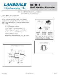
ML145146<br />
4–Bit Data Bus Input PLL<br />
Frequency Synthesizer<br />
INTERFACES WITH DUAL–MODULUS PRESCALERS<br />
Legacy Device: Motorola MC145146-2<br />
The ML145146 is programmed by a 4–bit input, with<br />
strobe and address lines. The device features consist of a<br />
reference oscillator, 12–bit programmable reference<br />
divider, digital phase detector, 10–bit programmable<br />
divide–by–N counter, 7–bit divide–by–A counter, and the<br />
necessary latch circuitry for accepting the 4–bit input data.<br />
• Operating Temperature Range: TA – 40 to +85°C<br />
• Low Power Consumption Through the Use of<br />
CMOS Technology<br />
• 3.0 to 9.0 V Supply Range<br />
• Programmable Reference Divider for Values Between<br />
3 and 4095<br />
• Dual–Modulus 4–Bit Data Bus Programming<br />
• ÷ N Range = 3 to 1023, ÷ A Range= 0 to 127<br />
• “Linearized” Digital Phase Detector Enhances<br />
Transfer Function Linearity<br />
• Two Error Signal Options:<br />
Single–Ended (Three–State)<br />
Double–Ended<br />
20<br />
20<br />
1<br />
1<br />
P DIP 20 = RP<br />
PLASTIC DIP<br />
CASE 738<br />
SOG 20 W = -6P<br />
SOG PACKAGE<br />
CASE 751D<br />
CROSS REFERENCE/ORDERING INFORMATION<br />
PACKAGE<br />
MOTOROLA<br />
<strong>LANSDALE</strong><br />
P DIP 20 MC145146P2 ML145146RP<br />
SOG 20W <strong>MC145146DW2</strong> ML145146-6P<br />
Note: Lansdale lead free (Pb) product, as it<br />
becomes available, will be identified by a part<br />
number prefix change from ML to MLE.<br />
D1<br />
D0<br />
PIN ASSIGNMENT<br />
1<br />
2<br />
20<br />
19<br />
D2<br />
D3<br />
fin<br />
3<br />
18<br />
fR<br />
BLOCK DIAGRAM<br />
VSS 4<br />
PDout 5<br />
17<br />
16<br />
φR<br />
φV<br />
VDD<br />
6<br />
15<br />
fV<br />
OSCin<br />
12–BIT ÷ R COUNTER<br />
fR<br />
OSCin<br />
7<br />
14<br />
MC<br />
OSCout<br />
D0<br />
D1<br />
D2<br />
D3<br />
A2<br />
A1<br />
A0<br />
ST<br />
LATCH<br />
CONTROL<br />
CIRCUITRY<br />
L5 L6 L7<br />
LATCHES<br />
L2 L3 L4 L0 L1<br />
LOCK<br />
DETECT<br />
PHASE<br />
DETECTOR A<br />
PHASE<br />
DETECTOR B<br />
LD<br />
PDout<br />
fV<br />
φV<br />
φR<br />
OSCout<br />
A0<br />
A1<br />
8<br />
9<br />
10<br />
13<br />
12<br />
11<br />
LD<br />
ST<br />
A2<br />
fin<br />
10–BIT ÷ N COUNTER<br />
7–BIT ÷ A COUNTER<br />
CONTROL LOGIC<br />
MODULUS CONTROL (MC)<br />
Page 1 of 12 www.lansdale.com<br />
Issue 0
ML145146<br />
<strong>LANSDALE</strong> <strong>Semiconductor</strong>, <strong>Inc</strong>.<br />
Page 2 of 12 www.lansdale.com<br />
Issue 0
ML145146<br />
<strong>LANSDALE</strong> <strong>Semiconductor</strong>, <strong>Inc</strong>.<br />
Page 3 of 12 www.lansdale.com<br />
Issue 0
ML145146<br />
<strong>LANSDALE</strong> <strong>Semiconductor</strong>, <strong>Inc</strong>.<br />
Page 4 of 12 www.lansdale.com<br />
Issue 0
ML145146<br />
<strong>LANSDALE</strong> <strong>Semiconductor</strong>, <strong>Inc</strong>.<br />
Page 5 of 12 www.lansdale.com<br />
Issue 0
ML145146<br />
PIN DESCRIPTIONS<br />
INPUT PINS<br />
D0 - D3<br />
Data Inputs (Pins 2, 1, 20, 19)<br />
Information at these inputs is transferred to the internal<br />
latches when the ST input is in the high state. D3 (Pin 19) is<br />
the most significant bit.<br />
fin<br />
Frequency Input (Pin 3)<br />
Input to ÷N portion of synthesizer fin is typically derived<br />
from loop VCO and is AC coupled into Pin 3. For larger<br />
amplitude signals (standard CMOS – logic levels) DC coupling<br />
may be used.<br />
OSCin/OSCout<br />
Reference Oscillator Input/Output (Pins 7 and 8)<br />
These pins form an on–chip reference oscillator when connected<br />
to terminals of an external parallel resonant crystal.<br />
Frequency setting capacitors of appropriate value must be connected<br />
from OSCin to ground and OSCout to ground. OSCin<br />
may also serve as input for an externally–generated reference<br />
signal. This signal is typically AC coupled to OSCin, but for<br />
larger amplitude signals (standard CMOS–logic levels) DC<br />
coupling may also be used. In the external reference mode, no<br />
connection is required to OSCout.<br />
A0 - A2<br />
Address Inputs (Pins 9, 10, 11)<br />
A0, A1 and A2 are used to define which latch receives the<br />
information on the data input lines. The addresses refer to the<br />
following latches.<br />
A2 A1 A0 Selected Function D0 D1 D2 D3<br />
0<br />
0<br />
0<br />
0<br />
1<br />
1<br />
1<br />
1<br />
0<br />
0<br />
1<br />
1<br />
0<br />
0<br />
1<br />
1<br />
0<br />
1<br />
0<br />
1<br />
0<br />
1<br />
0<br />
1<br />
Latch 0<br />
Latch 1<br />
Latch 2<br />
Latch 3<br />
Latch 4<br />
Latch 5<br />
Latch 6<br />
Latch 7<br />
÷ A Bits<br />
÷ A Bits<br />
÷ N Bits<br />
÷ N Bits<br />
÷ N Bits<br />
Reference Bits<br />
Reference Bits<br />
Reference Bits<br />
ST<br />
Strobe Transfer (Pin 12)<br />
The rising edge of strobe transfers data into the addressed<br />
latch. The falling edge of strobe latches data into the latch.<br />
This pin should normally be held low to avoid loading latches<br />
with invalid data.<br />
OUTPUT PINS<br />
PDout<br />
Single–ended Phase Detector Output (Pin 5)<br />
Three–state output of phase detector for use as loop error<br />
signal.<br />
Frequency fV>fR or fV Leading: Negative Pulses<br />
Frequency fV
ML145146<br />
<strong>LANSDALE</strong> <strong>Semiconductor</strong>, <strong>Inc</strong>.<br />
Page 7 of 12 www.lansdale.com<br />
Issue 0
ML145146<br />
<strong>LANSDALE</strong> <strong>Semiconductor</strong>, <strong>Inc</strong>.<br />
DESIGN CONSIDERATIONS<br />
CRYSTAL OSCILLATOR CONSIDERATIONS<br />
The following options may be considered to provide a reference<br />
frequency to Motorola’s CMOS frequency synthesizers.<br />
The most desirable is discussed first.<br />
Use of a Hybrid Crystal Oscillator<br />
Commercially available temperature–compensated crystal<br />
oscillators (TCXOs) or crystal–controlled data clock oscillators<br />
provide very stable reference frequencies. An oscillator<br />
capable of sinking and sourcing 50 µA at CMOS logic levels<br />
may be direct or DC coupled to OSCin. In general, the highest<br />
frequency capability is obtained utilizing a direct coupled<br />
square wave having a rail–to–rail (VDD to VSS) voltage<br />
swing. If the oscillator does not have CMOS logic levels on the<br />
outputs, capacitive or AC coupling of OSCin may be used.<br />
OSCout, an unbuffered output, should be left floating.<br />
For additional information about TCXOs and data clock<br />
oscillators, please consult the latest version of the eem<br />
Electronic Engineers Master Catalog, the Gold Book, or similar<br />
publications.<br />
Design an Off–Chip Reference<br />
The user may design and off–chip crystal oscillator using<br />
ICs specifically developed for crystal oscillator applications,<br />
such as the ML12061 MECL device. The reference signal from<br />
the MECL device is AC coupled to OSCin. For large amplitude<br />
signals (standard CMOS logic levels), DC coupling is<br />
used. OSCout, an unbuffered output, should be left floating. In<br />
general, the highest frequency capability is obtained with a<br />
direct–coupled square wave having rail–to–rail voltage swing.<br />
Use of the On–Chip Oscillator Circuitry<br />
The on–chip amplifier (a digital inverter) along with an<br />
appropriate crystal may be used to provide a reference source<br />
frequency. A fundamental mode crystal, parallel resonant at the<br />
desired operating frequency, should be connected as shown in<br />
Figure 8.<br />
For VDD = 5.0 V, the crystal should be specified for a loading<br />
capacitance. CL, which does not exceed 32 pF for frequencies<br />
to approximately 8.0 MHz, 20 pF for frequencies in the<br />
area of 8.0 to 15 MHz, and 10 pF for higher frequencies. These<br />
are guidelines that provide a reasonable compromise between<br />
IC capacitance, drive capability, swamping variations stray in<br />
IC input/output capacitance, and realistic CL values. The shunt<br />
load capacitance, CL, presented across the crystal can be estimated<br />
to be:<br />
The oscillator can be “trimmed” on–frequency by making a<br />
portion or all of C1 variable. The crystal and associated components<br />
must be located as close as possible to the OSCin and<br />
OSCout pins to minimize distortion, stray capacitance, stray<br />
inductance, and startup stabilization time. In some cases, stray<br />
capacitance should be added to the value for Cin and Cout.<br />
Power is dissipated in the effective series resistance of the<br />
crystal, Re. In Figure 10 The drive level specified by the crystal<br />
manufacturer is the maximum stress that a crystal can withstand<br />
without damaging or excessive shift in frequency. R1 in<br />
Figure 8 limits the drive level. The use of R1 may not be necessary<br />
in some cases (i.e. R1 = 0 ohms).<br />
To verify that the maximum DC supply voltage does not<br />
overdrive the crystal, monitor the output frequency as a function<br />
of voltage at OSCout. (care should be taken to minimize<br />
loading.) the frequency should increase very slightly as the dc<br />
supply voltage is increased. An overdriven crystal will decrease<br />
in frequency or become unstable with an increase in supply<br />
voltage. The operating supply voltage must be reduced or R1<br />
must be increased in value if the overdrive condition exists.<br />
The user should note that the oscillator start–up time is proportional<br />
to the value of R1.<br />
Through the process of supplying crystals for use with<br />
CMOS inverters, many crystal manufacturers have developed<br />
expertise in CMOS oscillator design with crystals. Discussions<br />
with such manufacturers can prove very helpful. See Table 1.<br />
where<br />
Cin = 5.0pF (See Figure 9)<br />
Cout = 6.0pF (See Figure 9)<br />
Ca = 1.0pF (See Figure 9)<br />
CO = the crystal’s holder capacitance (See Figure 10)<br />
C1 and C2 = external capacitors (See Figure 8)<br />
Page 8 of 12 www.lansdale.com<br />
Issue 0
ML145146<br />
<strong>LANSDALE</strong> <strong>Semiconductor</strong>, <strong>Inc</strong>.<br />
RECOMMENDED READING<br />
Technical Note TN–24 Statek Corp.<br />
Technical Note TN–7 Statek Corp.<br />
E. Hafner, “The Piezoelectric Crystal Unit – Definitions and<br />
Method of Measurement”, Proc. iEEE, Vol 57, No 2 Feb, 1969<br />
D. Kemper, L. Rosine, “Quartz Crystals for Frequency<br />
Control”, Electro–Tecchnology, June 1969<br />
P.J. Ottowitz, “AGuide to Crystal Selection”, Electronic<br />
Design, May 1966<br />
DUAL–MODULUS PRESCALING<br />
The technique of dual–modulus prescaling is well established<br />
as a method of acheiving high performance frequency<br />
synthesizer operation at high frequencies. Basically, the<br />
approach allows relatively low–frequency programmable counters<br />
to be used as high–frequency programmable counters with<br />
speed capability of several hundred MHz. This is possible<br />
without the sacrifice in system resolution and performance that<br />
results if a fixed (single–modulus) divider is used for the<br />
prescaler.<br />
In dual–modulus prescaling, the lower speed counters must<br />
be uniquely configured. Special control logic is necessary to<br />
select the divide value P or P ÷ 1 in the prescaler for the<br />
required amount of time (see modullus control definition).<br />
Lansdale’s dual–modulus frequency synthesizers contain this<br />
feature and can be used with a variety of dual–modulus<br />
prescalers to allow speed, complexity and cost to be tailored to<br />
the system requirements. Prescalers having P, P ÷ 1 divide values<br />
in the range of ÷3/÷4 to ÷128/÷129 can be controlled by<br />
most Lansdale frequency synthesizers.<br />
Several dual–modulus prescaler approaches suitable for use<br />
with the ML145146 are:<br />
ML12009<br />
ML12011<br />
ML12013<br />
ML12015<br />
ML12016<br />
ML12017<br />
ML12018<br />
ML12032<br />
DESIGN GUIDELINES<br />
÷5/÷6<br />
÷8/÷9<br />
÷10/÷11<br />
÷32/÷33<br />
÷40/÷41<br />
÷64/÷65<br />
÷128/÷129<br />
÷64/65 or ÷128/129<br />
440 MHz<br />
500 MHz<br />
500 MHz<br />
225 MHz<br />
225 MHz<br />
225 MHz<br />
520 MHz<br />
1.1 GHz<br />
The system total divide value. Ntotal (NT) will be dictated<br />
by the application. i.e.,<br />
N is the number programmed into the ÷N counter, A is the<br />
number programmed into the ÷A counter, P and P ÷ 1 are the<br />
two selectable divide ratios available in the dual–modulus<br />
prescalers. To have a range of NT values in sequence, the ÷A<br />
counter is programmed from zero through P ÷ 1 for a particular<br />
value N in the ÷N counter. N is then incremented to the N<br />
÷ 1, and the ÷A is sequenced from 0 through P ÷ 1 again.<br />
There are minimum and maximum values that can be<br />
achieved for NT. These values are a function of P and the size<br />
of the ÷N and ÷A counters. The constraint N ≥ A always<br />
applies. If Amax = P – 1, then Nmin ≥ P – 1. Then NTmin =<br />
(P – 1) P + A or (P – 1)P since A is free to assume the value of 0.<br />
NTmax ÷Nmax • P + Amax<br />
To maximize system frequency capability, the dual–modulus<br />
prescaler output must go from low to high after each group of<br />
P or P – 1 input cycles. The prescaler should divide by P when<br />
its modulus control line is high and by P – 1 when the modulus<br />
control is low.<br />
For the maximum frequency into the prescaler (fVCOmax),<br />
the value used for P must be large enough such that:<br />
1. f VCO max divided by P may not exceed the frequency<br />
capability of fin (input to the ÷N and ÷A counters).<br />
2. The period of fVCO divided by P must be greater than the<br />
sum of the times:<br />
a. Propagation delay through the dual modulus<br />
prescaler.<br />
b. Prescaler setup or release time relative to its modulus<br />
control signal.<br />
c. Propagation time from fin to the modulus control<br />
output for the frequency synthesizer device.<br />
A sometimes useful simplification in the programming code<br />
can be achieved by choosing the values for P of 8, 16, 32, or<br />
64. For these cases, the desired value of NT results when NT<br />
in binary is used as the program code to the ÷N and ÷A counters<br />
treated in the following manner:<br />
1. Assume the ÷A counter contains “a” bits where 2 a ≥P.<br />
2. Always program all higher order ÷A counter bits<br />
above “a” to 0<br />
3. Assume the ÷N counter and the ÷A counter (with all<br />
the higher order bits above “a” ignored) combined<br />
into a single binary counter of n + a bits in length (n =<br />
number of divider stages in the ÷N counter). The<br />
MSB of this “hypothetical” counter is to correspond to<br />
the MSB of ÷N and the LSB is to correspond to the<br />
LSB of ÷A. The system divide value, NT, now results<br />
when the value of NT in binary is used to program<br />
the “new” n + a bit counter.<br />
By using the two devices, several dual–modulus values are<br />
achievable (shown in Figure 11).<br />
Page 9 of 12 www.lansdale.com<br />
Issue 0
ML145146<br />
<strong>LANSDALE</strong> <strong>Semiconductor</strong>, <strong>Inc</strong>.<br />
APPLICATION<br />
The features of the ML145146 permit bus operation with a<br />
dedicated wire needed only for the strobe input. In a microprocessor–controlled<br />
system this strobe input is accessed<br />
when the phase lock loop is addressed. The remaining data<br />
and address inputs will directly interface to the microprocessor’s<br />
data and address buses.<br />
The device architecture allows the user to establish any<br />
integer reference divide value between 3 and 4095. The wide<br />
selection of ÷R values permits a high degree of flexibility in<br />
choosing the reference oscillator frequency. As a result the<br />
reference oscillator can frequently be chosen to serve multiple<br />
system functions such as a second local oscillator in a<br />
receiver design or a microprocessor system clock. Typical<br />
applications that take advantage of these ML145146 features<br />
including the dual modulus capability are shown in Figures<br />
12, 13 and 14.<br />
DEVICE A<br />
MC<br />
DEVICE B<br />
DEVICE<br />
B<br />
DEVICE A ML12009 ML12011 ML12013<br />
MC10131<br />
MC10138<br />
MC10154<br />
÷20/÷21<br />
÷50/÷51<br />
÷40/÷41<br />
OR<br />
÷80/÷81<br />
÷32/÷33<br />
÷80/÷81<br />
÷64/÷65<br />
OR<br />
÷128/÷129<br />
÷40/÷41<br />
÷100/÷101<br />
÷80/÷81<br />
NOTE: ML12009, ML12011 and ML12013 are pin equivalent.<br />
ML12015, ML12016 and ML12017 are pin equivalent.<br />
Figure 11. Dual Modulus Values<br />
Page 10 of 12 www.lansdale.com<br />
Issue 0
ML145146<br />
<strong>LANSDALE</strong> <strong>Semiconductor</strong>, <strong>Inc</strong>.<br />
CHOICE OF<br />
REF. OSC.<br />
FREQUENCY<br />
(ON–CHIP OSC.<br />
OPTIONAL)<br />
7<br />
6<br />
4<br />
8<br />
OSC out<br />
OSC in<br />
18 15 13<br />
f R f V LD<br />
PD out<br />
φ R<br />
V DD<br />
ML145146<br />
φ V<br />
V SS<br />
MOD<br />
CONTROL<br />
f in<br />
D3 D2 D1 D0 A2 A1 A0 ST<br />
19 20 1 2 11 10 9 12<br />
5<br />
3<br />
}<br />
17<br />
16<br />
14<br />
FOR USE WITH EXTERNAL<br />
PHASE DETECTOR (OPTIONAL)<br />
}<br />
LOCK DETECT<br />
SIGNAL<br />
LOOP<br />
FILTER<br />
CHOICE OF DETECTOR<br />
ERROR SIGNALS<br />
RECEIVER LO.<br />
443.325 443.950 MHz<br />
(25 kHz STEPS)<br />
VCO<br />
ML12034 PRESCALER<br />
TRANSMITTER<br />
MODULATION<br />
AND 15.7 MHz<br />
TRANSMITTER SIGNAL<br />
OFFSET<br />
459.025 – 459.650 MHz<br />
(25 kHz STEPS)<br />
CHIP<br />
TO SHARED CONTROLLER BUS SELECT TO<br />
NOTES:<br />
CONTROLLER<br />
1. Reciever I.F = 10.7 MHz, low side injection.<br />
2. Duplex operation with 5 MHz receive/transmit separation.<br />
3. f R = 25 kHz, + R chosen to correspond with desired reference oscillator frequency.<br />
4. N total = 17,733 to 17,758 = N • P + A; N = 227, A = 5 to 30 for P = 64.<br />
Figure 13. Synthesizer for UHF Mobil Radio Telephone Channels Demonstrates Use of the ML145146 in<br />
Microprocessor/Microcomputer Controlled Systems Operating to Several Hundred MHz<br />
CHOICE OF<br />
REF. OSC.<br />
FREQUENCY<br />
(ON–CHIP OSC.<br />
OPTIONAL)<br />
7<br />
6<br />
4<br />
8<br />
OSC out<br />
OSC in<br />
X3<br />
f R<br />
f V<br />
5<br />
LD<br />
PD out<br />
φ R<br />
V DD<br />
ML145146<br />
φ V<br />
16<br />
V SS<br />
MOD<br />
CONTROL<br />
f in<br />
14<br />
3<br />
D3 D2 D1 D0 A2 A1 A0 ST<br />
19 20 1 2 11 10 9 12<br />
TO SHARED CONTROLLER BUS<br />
CHIP<br />
SELECT TO<br />
CONTROLLER<br />
}<br />
17<br />
RECEIVER<br />
2ND, L.O.<br />
33,300 MHZ<br />
FOR USE WITH EXTERNAL<br />
PHASE DETECTOR (OPTIONAL)<br />
}<br />
LOCK DETECT<br />
SIGNAL<br />
LOOP<br />
FILTER<br />
CHOICE OF DETECTOR<br />
ERROR SIGNALS<br />
MC10131<br />
DUAL F/F<br />
RECEIVER FIRST L.O.<br />
825.030 844.980 MHZ<br />
(30 KHz STEPS)<br />
NOTES:<br />
1. Receiver 1st I.F. = 45 MHz, low side injection; Receiver 2nd I.F. = 11.7 MHz, low side injection.<br />
2. Duplex operation with 45 MHz receive/transmit separation.<br />
3. f R = 7.5 kHz, + R = 1480.<br />
4. N total = N • 32 + A = 27,501 to 28,166: N = 859 to 880; A = 0 to 31.<br />
5. Only one implementation is shown. Various other configurations and dual–modulus prescaling values to ÷128/÷129 are possible.<br />
Figure 14. 666 Channel, Computer Controlled, Mobile Radio Telephone Synthesizer for<br />
800 MHz Cellular Radio Systems<br />
VCO<br />
X4<br />
ML12011<br />
÷8/÷9 PRESCALER<br />
+32/+32 DUAL MODULUS PRESCALER<br />
TRANSMITTER<br />
MODULATION<br />
X4<br />
TRANSMITTER SIGNAL<br />
825.030 844.880 MHz<br />
(30 kHz STEPS)<br />
Page 11 of 12 www.lansdale.com<br />
Issue 0
ML145146<br />
<strong>LANSDALE</strong> <strong>Semiconductor</strong>, <strong>Inc</strong>.<br />
OUTLINE DIMENSIONS<br />
SOG = -6P<br />
(MC145146-6P)<br />
CASE 751D-04<br />
20<br />
11<br />
1 1 0<br />
-B-<br />
0.25 (0.010) M T B S A S<br />
K<br />
C<br />
P 10 PL<br />
0.25 (0.010) M B M<br />
J<br />
F<br />
M<br />
R X 45°<br />
NOTES:<br />
1. DIMENSIONING AND TOLERANCING PER ANSI<br />
Y14.5M, 1982<br />
2. CONTROLLING DIMENSION: MILLIMETER<br />
3. DIMENSIONA AND B DO NOT INCLUDE<br />
MOLD PROTRUSION.<br />
4. MAXIMUM MOLD PROTRUSION 0.150 (0.006)<br />
PER SIDE<br />
5. DIMENSION D DOES NOT INCLUDE DAMBAR<br />
PROTRUSION. ALLOWABLE DAMBAR<br />
PROTRUSION SHALL BE 0.13 (0.005) TOTAL, IN<br />
EXCESS OF D DIMENSION AT MAXIMUM<br />
MATERIAL CONDITION.<br />
DIM<br />
A<br />
B<br />
MIN<br />
12.65<br />
7.40<br />
INCHES<br />
MAX<br />
12.95<br />
7.60<br />
MILLIMETERS<br />
MAX<br />
0.510<br />
0.299<br />
MIN<br />
0.499<br />
0.292<br />
C 2.35 2.65 0.093 0.104<br />
D 0.35 0.49 0.014 0.019<br />
F 0.50 0.90 0.020 0.035<br />
G 1.27 BSC 0.050 BSC<br />
J 0.25 0.32 0.010 0.012<br />
K 0.10 0.25 0.020 0.035<br />
M<br />
P 10.05 10.56 .0395 0.415<br />
R 0.25 0.75 0.010 0.029<br />
PLASTIC DIP<br />
(MC145146RP)<br />
CASE 738-03<br />
-A-<br />
-T-<br />
-A-<br />
20<br />
11<br />
1 1 0<br />
B<br />
C<br />
L<br />
NOTES:<br />
1. DIMENSIONING AND TOLERANCING PER ANSI<br />
Y14.5M, 1982<br />
2. CONTROLLING DIMENSION: INCH<br />
3. DIMENSION L TO CENTER OF LEAD WHEN<br />
FORMED PARALLEL<br />
4. DIMENSION B DOES NOT INCLUDE MOLD<br />
FLASH<br />
-T-<br />
SEATING<br />
PLANE<br />
G<br />
E<br />
F<br />
D 20 PL<br />
N<br />
K<br />
0.25 (0.010) M T A<br />
M<br />
M<br />
J 20 PL<br />
0.25 (0.010) M T B<br />
M<br />
DIM<br />
A<br />
B<br />
C<br />
D<br />
E<br />
F<br />
G<br />
J<br />
K<br />
L<br />
M<br />
N<br />
INCHES MILLIMETERS<br />
MIN MAX MIN MAX<br />
1.010 1.070 25.66 27.17<br />
0.240 .0260 6.10 6.60<br />
0.150 0.180 3.81 4.57<br />
0.015 0.022 0.39 0.55<br />
0.050 BSC 1.27BSC<br />
0.050 0.070 1.27 1.77<br />
0.100 BSC 2.54 BSC<br />
0.008 0.015 0.21 0.38<br />
0.110 0.140 2.80 3.55<br />
0.300 BSC 7.62 BSC<br />
0.020<br />
0.040<br />
0.51<br />
1.01<br />
Lansdale <strong>Semiconductor</strong> reserves the right to make changes without further notice to any products herein to improve reliability,<br />
function or design. Lansdale does not assume any liability arising out of the application or use of any product or circuit<br />
described herein; neither does it convey any license under its patent rights nor the rights of others. “Typical” parameters which<br />
may be provided in Lansdale data sheets and/or specifications can vary in different applications, and actual performance may<br />
vary over time. All operating parameters, including “Typicals” must be validated for each customer application by the customer’s<br />
technical experts. Lansdale <strong>Semiconductor</strong> is a registered trademark of Lansdale <strong>Semiconductor</strong>, <strong>Inc</strong>.<br />
Page 12 of 12 www.lansdale.com<br />
Issue 0