MC13155D - LANSDALE Semiconductor Inc.
MC13155D - LANSDALE Semiconductor Inc.
MC13155D - LANSDALE Semiconductor Inc.

Create successful ePaper yourself
Turn your PDF publications into a flip-book with our unique Google optimized e-Paper software.
ML13155<br />
Wideband FM IF<br />
SEMICONDUCTOR TECHNICAL DATA<br />
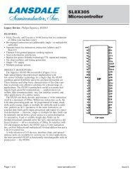
Legacy Device: Motorola MC13155<br />
The ML13155 is a complete wideband FM detector designed for<br />
satellite TV and other wideband data and analog FM applications.<br />
This device may be cascaded for higher IF gain and<br />
extended Receive Signal Strength Indicator (RSSI) range.<br />
• 12 MHz Video/Baseband Demodulator<br />
• Ideal for Wideband Data and Analog FM Systems<br />
• Limiter Output for Cascade Operation<br />
• Low Drain Current: 7.0 mA<br />
• Low Supply Voltage: 3.0 to 6.0 V<br />
• Operates to 300 Mhz<br />
• Operating Temperature Range TA = –40 to +85°C<br />
MAXIMUM RATINGS<br />
Rating Pin Symbol Value Unit<br />
Power Supply Voltage 11, 14 VEE (max) 6.5 Vdc<br />
Input Voltage 1, 16 Vin 1.0 Vrms<br />
Junction Temperature – TJ +150 °C<br />
Storage Temperature Range – Tstg – 65 to +150 °C<br />
16<br />
1<br />
SO–16 = -5P<br />
PLASTIC PACKAGE<br />
CASE 751B<br />
(SO–16)<br />
CROSS REFERENCE/ORDERING INFORMATION<br />
PACKAGE MOTOROLA <strong>LANSDALE</strong><br />
SO 16 <strong>MC13155D</strong> ML13155-5P<br />
Note: Lansdale lead free (Pb) product, as it<br />
becomes available, will be identified by a part<br />
number prefix change from ML to MLE.<br />
NOTE:<br />
Devices should not be operated at or outside these values. The “Recommended<br />
Operating Conditions” provide for actual device operation.<br />
PIN CONNECTIONS<br />
Figure 1. Representative Block Diagram<br />
Input<br />
1<br />
16<br />
Input<br />
Decouple<br />
2<br />
15<br />
Decouple<br />
Decouple<br />
15<br />
Buffered<br />
RSSI<br />
Output<br />
13<br />
RSSI<br />
Output<br />
12<br />
Limiter<br />
Output<br />
10<br />
VCC1<br />
Output<br />
3<br />
4<br />
14<br />
13<br />
VEE1<br />
RSSI Buffer<br />
Output<br />
5<br />
12<br />
RSSI<br />
Input<br />
Input<br />
16<br />
1<br />
Three Stage<br />
Amplifier<br />
Detector<br />
9<br />
8<br />
Quad<br />
Coil<br />
VCC2<br />
Limiter Out<br />
Quad Coil<br />
6<br />
7<br />
8<br />
11<br />
10<br />
9<br />
VEE2<br />
Limiter Out<br />
Quad Coil<br />
(Top View)<br />
2<br />
Decouple<br />
4<br />
Balanced<br />
Outputs<br />
5<br />
7<br />
Limiter<br />
Output<br />
NOTE: This device requires careful layout and decoupling to ensure stable operation.<br />
Page 1 of 16<br />
www.lansdale.com<br />
Issue A
ML13155<br />
<strong>LANSDALE</strong> <strong>Semiconductor</strong>, <strong>Inc</strong>.<br />
RECOMMENDED OPERATING CONDITIONS<br />
Rating Pin Symbol Value Unit<br />
Power Supply Voltage (TA= 25°C) 11, 14 VEE – 3.0 to – 6.0 Vdc<br />
– 40C ≤ TA ≤ 85°C 3, 6 VCC Grounded<br />
Maximum Input Frequency 1, 16 fin 300 MHz<br />
Ambient Temperature Range – TJ – 40 to + 85 °C<br />
DC ELECTRICAL CHARACTERISTICS (TA = 25°C, no input signal.)<br />
Characteristic Pin Symbol Min Typ Max Unit<br />
Drain Current 11 I11 2.0 2.8 4.0 mA<br />
(VEE = – 5.0 Vdc) 14 I14 3.0 4.3 6.0<br />
(VEE = – 5.0 Vdc) 14 I14 3.0 4.3 6.0<br />
Drain Current Total (see Figure 3) 11, 14 ITotal 5.0 7.1 10 mA<br />
(VEE = – 5.0 Vdc) 5.0 7.5 10.5<br />
(VEE = – 6.0 Vdc) 5.0 7.5 10.5<br />
(VEE = – 3.0 Vdc) 4.7 6.6 9.5<br />
AC ELECTRICAL CHARACTERISTICS (TA = 25°C, fIF = 70 MHz, VEE = – 5.0 Vdc Figure 2, unless otherwise noted.)<br />
Characteristic Pin Min Typ Max Unit<br />
Input for – 3 dB Limiting Sensitivity 1, 16 – 1.0 2.0 mVrms<br />
Differential Detector Output Voltage (Vin = 10 mVrms) 4, 5 mVp–p<br />
(fdev = ± 3.0 MHz) (VEE = – 6.0 Vdc) 470 590 700<br />
(VEE = – 5.0 Vdc) 450 570 680<br />
(VEE = – 3.0 Vdc) 380 500 620<br />
Detector DC Offset Voltage 4, 5 – 250 – 250 mVdc<br />
RSSI Slope 13 1.4 2.1 2.8 µA/dB<br />
RSSI Dynamic Range 13 31 35 39 dB<br />
RSSI Output 12 µA<br />
(Vin = 100 µVrms) – 2.1 –<br />
(Vin = 1.0 mVrms) – 2.4 –<br />
(Vin = 10 mVrms) 16 24 36<br />
(Vin = 100 mVrms) – 65 –<br />
(Vin = 500 mVrms) – 75 –<br />
RSSI Buffer Maximum Output Current (Vin = 10 mVrms) 13 – 2.3 – mAdc<br />
Differential Limiter Output<br />
(Vin = 1.0 mVrms) 7, 10 100 140 –<br />
(Vin = 10 mVrms) – 180 –<br />
Demodulator Video 3.0 dB Bandwidth 4, 5 – 12 – MHz<br />
Input Impedance (Figure 14) 1, 16<br />
@ 70 MHz Rp (VEE = – 5.0 Vdc) – 450 – Ω<br />
@ 70 MHz Cp (C2=C15 = 100 p) – 4.8 – pF<br />
Differential IF Power Gain 1, 7, 10, 16 – 46 – dB<br />
mVrms<br />
NOTE:<br />
Positive currents are out of the pins of the device.<br />
Page 2 of 16<br />
www.lansdale.com<br />
Issue A
ML13155<br />
<strong>LANSDALE</strong> <strong>Semiconductor</strong>, <strong>Inc</strong>.<br />
The ML13155 consists of a wideband three–stage limiting<br />
amplifier, a wideband quadrature detector which may be<br />
operated up to 200 MHz, and a received signal strength<br />
CIRCUIT DESCRIPTION<br />
indicator (RSSI) circuit which provides a current output linearly<br />
proportional to the IF input signal level for approximately<br />
35 dB range of input level.<br />
Figure 2. Test Circuit<br />
Vin<br />
1.0n<br />
1<br />
IN1<br />
IN2<br />
16<br />
1.0n<br />
27<br />
49.9<br />
2<br />
DEC1<br />
DEC2<br />
15<br />
10n<br />
Video<br />
Output<br />
3<br />
4<br />
5<br />
VCC1<br />
DETO1<br />
DETO2<br />
VEE1<br />
RSSI<br />
Buffer<br />
RSSI<br />
14<br />
13<br />
12<br />
1.0n<br />
1.0n<br />
100n<br />
1.0k<br />
10µ<br />
+<br />
VEE<br />
VEE<br />
Limiter 1<br />
Output<br />
1.0n<br />
330<br />
6<br />
7<br />
8<br />
VCC2<br />
LIMO1<br />
QUAD1<br />
VEE2<br />
LIMO2<br />
QUAD2<br />
11<br />
10<br />
9<br />
1.0n<br />
1.0n<br />
100n<br />
330<br />
Limiter 2<br />
Output<br />
10µ<br />
+<br />
VEE<br />
499<br />
20p<br />
L1<br />
L1 – Coilcraft part number 146–09J08S<br />
260n<br />
APPLICATIONS INFORMATION<br />
EVALUATION PC BOARD<br />
The evaluation PCB shown in Figures 19 and 20 is very versatile<br />
and is designed to cascade two ICs. The center section<br />
of the board provides an area for attaching all surface mount<br />
components to the circuit side and radial leaded components<br />
to the component ground side of the PCB (see Figures 17 and<br />
18). Additionally, the peripheral area surrounding the RF<br />
core provides pads to add supporting and interface circuitry<br />
as a particular application dictates. This evaluation board will<br />
be discussed and referenced in this section.<br />
LIMITING AMPLIFIER<br />
Differential input and output ports interfacing the three stage<br />
limiting amplifier provide a differential power gain of typically<br />
46 dB and useable frequency range of 300 MHz. The IF<br />
gain flatness may be controlled by decoupling of the internal<br />
feedback network at Pins 2 and 15.<br />
Scattering parameter (S–parameter) characterization of the IF<br />
as a two port linear amplifier is useful to implement maximum<br />
stable power gain, input matching, and stability over a<br />
desired bandpass response and to ensure stable operation outside<br />
the bandpass as well. The ML13155 is unconditionally<br />
stable over most of its useful operating frequency range; however,<br />
it can be made unconditionally stable over its entire<br />
operating range with the proper decoupling of Pins 2 and 15.<br />
Relatively small decoupling capacitors of about 100 pF have a<br />
significant effect on the wideband response and stability.<br />
This is shown in the scattering parameter tables where<br />
S–parameters are shown for various values of C2 and C15<br />
and at VEE of –3.0 and –5.0 V DC.<br />
Page 3 of 16<br />
www.lansdale.com<br />
Issue A
ML13155<br />
<strong>LANSDALE</strong> <strong>Semiconductor</strong>, <strong>Inc</strong>.<br />
I 11 and I 14 , TOTAL DRAIN CURRENT (mAdc)<br />
I 14 and I Total , DRAIN CURRENT (mAdc)<br />
10<br />
8.0<br />
6.0<br />
4.0<br />
2.0<br />
0.0<br />
0.0<br />
9.0<br />
8.5<br />
8.0<br />
7.5<br />
7.0<br />
6.5<br />
6.0<br />
Figure 3. Drain Current versus Supply Voltage<br />
TA = 25°C<br />
ITotal = I14 + I11<br />
– 5.0 Vdc<br />
RSSI OUTPUT ( A)<br />
12 µ<br />
I ,<br />
– 40 dBm<br />
0<br />
1.0 2.0 3.0 4.0 5.0 6.0 7.0 8.0 10<br />
100 1000<br />
VEE, SUPPLY VOLTAGE (–Vdc)<br />
Figure 5. Total Drain Current versus Ambient<br />
Temperature and Supply Voltage<br />
I14<br />
VEE = – 6.0 Vdc<br />
– 3.0 Vdc<br />
TA, AMBIENT TEMPERATURE (°C)<br />
TYPICAL PERFORMANCE AT TEMPERATURE<br />
(See Figure 2. Test Circuit)<br />
DRAIN CURRENT (mAdc)<br />
I 14 and I 11 ,<br />
5.5 2.5<br />
Figure 4. RSSI Output versus Frequency and<br />
Input Signal Level<br />
0 dBm<br />
–10 dBm<br />
– 20 dBm<br />
– 30 dBm<br />
VEE = – 5.0Vdc<br />
f, FREQUENCY (MHz)<br />
Figure 6. Detector Drain Current and Limiter<br />
Drain Current versus Ambient Temperature<br />
f = 70 MHz<br />
VEE = – 5.0 Vdc<br />
5.0<br />
2.0<br />
– 50 – 30 –10 10 30 50 70 90 110 – 50 – 30 –10 10 30 50 70 90 110<br />
100<br />
80<br />
60<br />
40<br />
20<br />
5.5<br />
5.0<br />
4.5<br />
4.0<br />
3.5<br />
3.0<br />
I11<br />
TA, AMBIENT TEMPERATURE (°C)<br />
I14<br />
RSSI OUTPUT ( µ A)<br />
I ,<br />
12<br />
25.0<br />
24.5<br />
24.0<br />
23.5<br />
23.0<br />
22.5<br />
22.0<br />
Figure 7. RSSI Output versus Ambient<br />
Temperature and Supply Voltage<br />
VEE = – 6.0 Vdc<br />
VEE = – 5.0 Vdc<br />
VEE = – 3.0 Vdc<br />
RSSI OUTPUT ( µ A)<br />
I ,<br />
12<br />
100<br />
80<br />
60<br />
40<br />
20<br />
Figure 8. RSSI Output versus Input Signal<br />
Voltage (Vin at Temperature)<br />
TA = + 85°C<br />
+ 25°C<br />
– 40°C<br />
21.5<br />
– 50<br />
0<br />
– 30 – 10 10 30 50 70 90 110 0.1<br />
1.0 10 100 1000<br />
TA, AMBIENT TEMPERATURE (°C)<br />
Vin, INPUT VOLTAGE (mVrms)<br />
Page 4 of 16<br />
www.lansdale.com<br />
Issue A
ML13155<br />
<strong>LANSDALE</strong> <strong>Semiconductor</strong>, <strong>Inc</strong>.<br />
DIFFERENTIAL DETECTOR OUTPUT VOLTAGE<br />
(Pins 4, 5), (mV pp )<br />
Figure 9. Differential Detector Output<br />
Voltage versus Ambient Temperature<br />
and Supply Voltage<br />
750 220<br />
VEE = – 6.0 Vdc<br />
700<br />
– 5.0 Vdc<br />
200<br />
650<br />
– 3.0 Vdc<br />
600<br />
180<br />
550<br />
500<br />
450<br />
400<br />
TA, AMBIENT TEMPERATURE (C)<br />
DIFFERENTIAL LIMITER OUTPUT VOLTAGE<br />
(Pins 7, 10), (mVrms)<br />
Figure 10. Differential Limiter Output Voltage<br />
versus Ambient Temperature<br />
(Vin = 1 and 10 mVrms)<br />
Vin = 10 mVrms<br />
350<br />
120<br />
– 50 – 30 –10 10 30 50 70 90 110 – 50 – 30 –10 10 30 50 70 90<br />
160<br />
140<br />
f = 70 MHz<br />
VEE = – 5.0 Vdc<br />
TA, AMBIENT TEMPERATURE (C)<br />
Vin = 1.0 mVrms<br />
DIFFERENTIAL DETECTOR OUTPUT (mV pp )<br />
1600<br />
1400<br />
1200<br />
1000<br />
800<br />
600<br />
400<br />
200<br />
0<br />
1.5<br />
Figure 11A. Differential Detector Output Voltage<br />
versus Q of Quadrature LC Tank<br />
Vin = – 30 dBm<br />
VEE = – 5.0 Vdc<br />
fc = 70 MHz<br />
fmod = 1.0 MHz<br />
(Figure 16 no external capacitors<br />
between Pins 7, 8 and 9, 10)<br />
Q OF QUADRATURE LC TANK<br />
Figure 11.<br />
f dev = ± 6.0 MHz<br />
± 5.0 MHz<br />
±4.0 MHz<br />
± 3.0 MHz<br />
± 2.0 MHz<br />
± 1.0 MHz<br />
)<br />
DIFFERENTIAL DETECTOR OUTPUT (mV pp<br />
2400<br />
2000<br />
1600<br />
1200<br />
Figure 11B. Differential Detector Output Voltage<br />
versus Q of Quadrature LC Tank<br />
Vin = – 30 dBm<br />
VEE = – 5.0 Vdc<br />
fc = 70 MHz<br />
fmod = 1.0 MHz<br />
(Figure 16 no external capacitors<br />
between Pins 7, 8 and 9, 10)<br />
Q OF QUADRATURE LC TANK<br />
f dev = ± 6.0 MHz<br />
± 5.0 MHz<br />
± 4.0 MHz<br />
± 3.0 MHz<br />
± 2.0 MHz<br />
± 1.0 MHz<br />
0<br />
2.0 2.5 3.0 3.5 4.0 4.5 5.0 5.5 6.0 1.5 2.0 2.5 3.0 3.5 4.0 4.5 5.0 5.5 6.0<br />
800<br />
400<br />
RSSI OUTPUT VOLTAGE, (Vdc)<br />
0<br />
– 1.0<br />
– 2.0<br />
– 3.0<br />
– 4.0<br />
– 5.0<br />
Figure 12. RSSI Output Voltage versus IF Input<br />
VEE = – 5.0 Vdc<br />
fc = 70 MHz<br />
(See Figure 16)<br />
Capacitively coupled<br />
interstage: no attenuation<br />
– 80 – 60 – 40 – 20 0 20<br />
IF INPUT, (dBm)<br />
15 dB Interstage<br />
Attenuator<br />
S+N, N (dB)<br />
10<br />
0<br />
–10<br />
– 20<br />
– 30<br />
– 40<br />
Figure 13. S+N, N versus IF Input<br />
S+N<br />
– 50<br />
fc = 70 MHz<br />
N<br />
fmod = 1.0 MHz<br />
– 60 fdev = ± 5.0 MHz<br />
VEE = – 5.0 Vdc<br />
– 70<br />
– 90 – 70 – 50 – 30 – 10 10<br />
IF INPUT (dBm)<br />
Page 5 of 16<br />
www.lansdale.com<br />
Issue A
ML13155<br />
<strong>LANSDALE</strong> <strong>Semiconductor</strong>, <strong>Inc</strong>.<br />
In the S–parameters measurements, the IF is treated as a<br />
two–port linear class A amplifier. The IF amplifier is measured<br />
with a single–ended input and output configuration in<br />
which the Pins 16 and 7 are terminated in the series combination<br />
of a 47 resistor and a 10 nF capacitor to VCC ground<br />
(see Figure 14. S–Parameter Test Circuit).<br />
The S–parameters are in polar form a the magnitude (MAG)<br />
and angle (ANG). Also listed in the tables are the calculated<br />
values for the stability and factor (K) and the Maximum<br />
Available Gain (MAG). These terms are related in the following<br />
equations:<br />
K = (1–IS11 I2–IS22I2 + I∆I2)/(2 I S12 S21 I)<br />
where: I ∆ I = I S11 S22–S12 S21 I.<br />
MAG = 10 log I S21 I/I S12 I + 10 log I K–(K2–1)1/2 I<br />
where: K >1. The necessary and sufficient conditions for<br />
unconditional stability are given as K>1:<br />
B1 = 1 + I S11 I2 – I S22 I2 – I ∆ I2 > 0<br />
Figure 14. S–Parameter Test Circuit<br />
IF<br />
Input<br />
SMA<br />
1.0n<br />
C2<br />
1<br />
2<br />
IN1<br />
DEC1<br />
IN2<br />
DEC2<br />
16<br />
15<br />
1.0n<br />
C15<br />
47<br />
3<br />
VCC1<br />
VEE1<br />
14<br />
VEE<br />
4<br />
DETO1<br />
RSSI<br />
Buffer<br />
13<br />
1.0n<br />
100n<br />
10µ<br />
+<br />
5<br />
DETO2<br />
RSSI<br />
12<br />
47<br />
1.0n<br />
6<br />
7<br />
8<br />
VCC2<br />
LIMO1<br />
QUAD1<br />
VEE2<br />
LIMO2<br />
QUAD2<br />
11<br />
10<br />
9<br />
1.0n<br />
SMA<br />
IF<br />
Output<br />
Page 6 of 16<br />
www.lansdale.com<br />
Issue A
ML13155<br />
<strong>LANSDALE</strong> <strong>Semiconductor</strong>, <strong>Inc</strong>.<br />
S–Parameters (VEE = – 5.0 Vdc, TA = 25°C, C2 and C15 = 0 pF)<br />
Frequency Input S11 Forward S21 Rev S12 Output S22 K MAG<br />
MHz MAG ANG MAG ANG MAG ANG MAG ANG MAG dB<br />
1.0 0.94 –13 8.2 143 0.001 7.0 0.87 – 22 2.2 32<br />
2.0 0.78 –2 3 23.5 109 0.001 – 40 0.64 – 31 4.2 33.5<br />
5.0 0.48 1.0 39.2 51 0.001 – 97 0.34 –17 8.7 33.7<br />
7.0 0.59 15 40.3 34 0.001 – 41 0.33 –13 10.6 34.6<br />
10 0.75 17 40.9 19 0.001 – 82 0.41 –1.0 5.7 36.7<br />
20 0.95 7.0 42.9 – 6.0 0.001 – 42 0.45 0 1.05 46.4<br />
50 0.98 –10 42.2 – 48 0.001 – 9.0 0.52 – 3.0 0.29 –<br />
70 0.95 –16 39.8 – 68 0.001 112 0.54 –16 1.05 46.4<br />
100 0.93 –2 3 44.2 – 93 0.001 80 0.53 – 22 0.76 –<br />
150 0.91 –3 4 39.5 –139 0.001 106 0.50 – 34 0.94 –<br />
200 0.87 –4 7 34.9 –179 0.002 77 0.42 – 44 0.97 –<br />
500 0.89 –103 11.1 – 58 0.022 57 0.40 –117 0.75 –<br />
700 0.61 –156 3.5 –164 0.03 0 0.52 179 2.6 13.7<br />
900 0.56 162 1.2 92 0.048 – 44 0.47 112 4.7 4.5<br />
1000 0.54 131 0.8 42 0.072 – 48 0.44 76 5.1 0.4<br />
S–Parameters (VEE = – 5.0 Vdc, TA = 25°C, C2 and C15 = 100 pF)<br />
Frequency Input S11 Forward S21 Rev S12 Output S22 K MAG<br />
MHz MAG ANG MAG ANG MAG ANG MAG ANG MAG dB<br />
1.0 0.98 –15 11.7 174 0.001 –14 0.84 – 27 1.2 37.4<br />
2.0 0.50 – 2.0 39.2 85.5 0.001 –108 0.62 – 35 6.0 35.5<br />
5.0 0.87 8.0 39.9 19 0.001 100 0.47 – 9.0 4.2 39.2<br />
7.0 0.90 5.0 40.4 9.0 0.001 – 40 0.45 – 8.0 3.1 40.3<br />
10 0.92 3.0 41 1.0 0.001 – 40 0.44 – 5.0 2.4 41.8<br />
20 0.92 – 2.0 42.4 –14 0.001 – 87 0.49 – 6.0 2.4 41.9<br />
50 0.91 – 8.0 41.2 – 45 0.001 85 0.50 – 5.0 2.3 42<br />
70 0.91 –11 39.1 – 63 0.001 76 0.52 – 4.0 2.2 41.6<br />
100 0.91 –15 43.4 – 84 0.001 85 0.50 –11 1.3 43.6<br />
150 0.90 – 22 38.2 –126 0.001 96 0.43 – 22 1.4 41.8<br />
200 0.86 – 33 35.5 –160 0.002 78 0.43 – 21 1.3 39.4<br />
500 0.80 – 66 8.3 – 9.0 0.012 75 0.57 – 63 1.7 23.5<br />
700 0.62 – 96 2.9 – 95 0.013 50 0.49 –111 6.3 12.5<br />
900 0.56 –120 1.0 –171 0.020 53 0.44 –150 13.3 2.8<br />
1000 0.54 –136 0.69 154 0.034 65 0.44 –179 12.5 – 0.8<br />
Page 7 of 16<br />
www.lansdale.com<br />
Issue A
ML13155<br />
<strong>LANSDALE</strong> <strong>Semiconductor</strong>, <strong>Inc</strong>.<br />
S–Parameters (VEE = – 5.0 Vdc, TA = 25°C, C2 and C15 = 680 pF)<br />
Frequency Input S11 Forward S21 Rev S12 Output S22 K MAG<br />
MHz MAG ANG MAG ANG MAG ANG MAG ANG MAG dB<br />
1.0 0.74 4.0 53.6 110 0.001 101 0.97 – 35 0.58 –<br />
2.0 0.90 3.0 70.8 55 0.001 60 0.68 – 34 1.4 45.6<br />
5.0 0.91 0 87.1 21 0.001 –121 0.33 – 60 1.1 49<br />
7.0 0.91 0 90.3 11 0.001 –18 0.25 – 67 1.2 48.4<br />
10 0.91 – 2.0 92.4 2.0 0.001 33 0.14 – 67 1.5 47.5<br />
20 0.91 – 4.0 95.5 –16 0.001 63 0.12 –15 1.3 48.2<br />
50 0.90 – 8.0 89.7 – 50 0.001 – 43 0.24 26 1.8 46.5<br />
70 0.90 –10 82.6 –70 0.001 92 0.33 21 1.4 47.4<br />
100 0.91 –14 77.12 –93 0.001 23 0.42 –1.0 1.05 49<br />
150 0.94 – 20 62.0 –122 0.001 96 0.42 – 22 0.54 –<br />
200 0.95 – 33 56.9 –148 0.003 146 0.33 – 62 0.75 –<br />
500 0.82 – 63 12.3 –12 0.007 79 0.44 – 67 1.8 26.9<br />
700 0.66 – 98 3.8 –107 0.014 84 0.40 –115 4.8 14.6<br />
900 0.56 –122 1.3 177 0.028 78 0.39 –166 8.0 4.7<br />
1000 0.54 –139 0.87 141 0.048 76 0.41 165 7.4 0.96<br />
S–Parameters (VEE = – 3.0 Vdc, TA = 25°C, C2 and C15 = 0 pF)<br />
Frequency Input S11 Forward S21 Rev S12 Output S22 K MAG<br />
MHz MAG ANG MAG ANG MAG ANG MAG ANG MAG dB<br />
1.0 0.89 –14 9.3 136 0.001 2.0 0.84 – 27 3.2 30.7<br />
2.0 0.76 – 22 24.2 105 0.001 – 90 0.67 – 37 3.5 34.3<br />
5.0 0.52 5.0 35.7 46 0.001 – 32 0.40 –13 10.6 33.3<br />
7.0 0.59 12 38.1 34 0.001 – 41 0.40 –10 9.1 34.6<br />
10 0.78 15 37.2 16 0.001 – 92 0.40 –1.0 5.7 36.3<br />
20 0.95 5.0 38.2 – 9.0 0.001 47 0.51 – 4.0 0.94 –<br />
50 0.96 –11 39.1 – 50 0.001 –103 0.48 – 6.0 1.4 43.7<br />
70 0.93 –17 36.8 – 71 0.001 – 76 0.52 –13 2.2 41.4<br />
100 0.91 – 25 34.7 – 99 0.001 –152 0.51 –19 3.0 39.0<br />
150 0.86 – 37 33.8 –143 0.001 53 0.49 – 34 1.7 39.1<br />
200 0.81 – 49 27.8 86 0.003 76 0.55 – 56 2.4 35.1<br />
500 0.70 – 93 6.2 – 41 0.015 93 0.40 –110 2.4 19.5<br />
700 0.62 –144 1.9 –133 0.049 56 0.40 –150 3.0 8.25<br />
900 0.39 –176 0.72 125 0.11 –18 0.25 163 5.1 –1.9<br />
1000 0.44 166 0.49 80 0.10 – 52 0.33 127 7.5 – 4.8<br />
Page 8 of 16<br />
www.lansdale.com<br />
Issue A
ML13155<br />
<strong>LANSDALE</strong> <strong>Semiconductor</strong>, <strong>Inc</strong>.<br />
S–Parameters (VEE = – 3.0 Vdc, TA = 25°C, C2 and C15 = 100 pF)<br />
Frequency Input S11 Forward S21 Rev S12 Output S22 K MAG<br />
MHz MAG ANG MAG ANG MAG ANG MAG ANG MAG dB<br />
1.0 0.97 –15 11.7 171 0.001 – 4.0 0.84 – 27 1.4 36.8<br />
2.0 0.53 2.0 37.1 80 0.001 – 91 0.57 – 31 6.0 34.8<br />
5.0 0.88 7.0 37.7 18 0.001 – 9.0 0.48 – 7.0 3.4 39.7<br />
7.0 0.90 5.0 37.7 8.0 0.001 –11 0.49 – 7.0 2.3 41<br />
10 0.92 2.0 38.3 1.0 0.001 – 59 0.51 – 9.0 2.0 41.8<br />
20 0.92 – 2.0 39.6 –15 0.001 29 0.48 – 3.0 1.9 42.5<br />
50 0.91 – 8.0 38.5 – 46 0.001 – 21 0.51 – 7.0 2.3 41.4<br />
70 0.91 –11 36.1 – 64 0.001 49 0.50 – 8.0 2.3 40.8<br />
100 0.91 –15 39.6 – 85 0.001 114 0.52 –13 1.7 37.8<br />
150 0.89 – 22 34.4 –128 0.001 120 0.48 – 23 1.6 40.1<br />
200 0.86 – 33 32 –163 0.002 86 0.40 – 26 1.7 37.8<br />
500 0.78 – 64 7.6 –12 0.013 94 0.46 – 71 1.9 22.1<br />
700 0.64 – 98 2.3 –102 0.027 58 0.42 –109 4.1 10.1<br />
900 0.54 –122 0.78 179 0.040 38.6 0.35 –147 10.0 – 0.14<br />
1000 0.53 –136 0.47 144 0.043 23 0.38 –171 15.4 – 4.52<br />
S–Parameters (VEE = – 3.0 Vdc, TA = 25°C, C2 and C15 = 680 pF)<br />
Frequency Input S11 Forward S21 Rev S12 Output S22 K MAG<br />
MHz MAG ANG MAG ANG MAG ANG MAG ANG MAG dB<br />
1.0 0.81 3.0 37 101 0.001 –19 0.90 – 32 1.1 43.5<br />
2.0 0.90 2.0 47.8 52.7 0.001 – 82 0.66 – 39 0.72 –<br />
5.0 0.91 0 58.9 20 0.001 104 0.37 – 56 2.3 44<br />
7.0 0.90 –1 60.3 11 0.001 – 76 0.26 – 55 2.04 44<br />
10 0.91 – 2.0 61.8 3.0 0.001 105 0.18 – 52 2.2 43.9<br />
20 0.91 – 4.0 63.8 – 15 0.001 59 0.11 –13 2.0 44.1<br />
50 0.90 – 8.0 60.0 – 48 0.001 96 0.22 33 2.3 43.7<br />
70 0.90 –11 56.5 – 67 0.001 113 0.29 15 2.3 43.2<br />
100 0.91 –14 52.7 – 91 0.001 177 0.36 5.0 2.0 43<br />
150 0.93 – 21 44.5 –126 0.001 155 0.35 –17 1.8 42.7<br />
200 0.90 – 43 41.2 –162 0.003 144 0.17 – 31 1.6 34.1<br />
500 0.79 – 65 7.3 –13 0.008 80 0.44 – 75 3.0 22<br />
700 0.65 – 97 2.3 –107 0.016 86 0.38 –124 7.1 10.2<br />
900 0.56 –122 0.80 174 0.031 73 0.38 –174 12 0.37<br />
1000 0.55 –139 0.52 137 0.50 71 0.41 157 11.3 – 3.4<br />
Page 9 of 16<br />
www.lansdale.com<br />
Issue A
ML13155<br />
<strong>LANSDALE</strong> <strong>Semiconductor</strong>, <strong>Inc</strong>.<br />
DC BIASING CONSIDERATIONS<br />
The DC biasing scheme utilizes two VCC connections (Pins 3 and<br />
6) and two VEE connections (Pins 14 and 11). VEE1 (Pin 14) is<br />
connected internally to the IF and RSSI circuits’ negative supply bus<br />
while the VEE2 (Pin 11) is connected internally to the quadrature<br />
detector’s negative bus. Under positive ground operation, this<br />
unique configuration offers the ability to bias the RSSI and IF separately<br />
from the quadrature detector. When two ICs are cascaded as<br />
shown in the 70 MHz application circuit and provided by the PCB<br />
(see Figures 17 and 18), the first ML13155 is used without biasing<br />
its quadrature detector, thereby saving approximately 3.0 mA. A<br />
total current of 7.0 mA is used to fully bias each IC, thus the total<br />
current in the application circuit is approximately 11 mA. Both VCC<br />
pins are biased by the same supply. VCC1 (Pin 3) is connected internally<br />
to the positive bus of the first half of the IF limiting amplifier,<br />
while VCC2 is internally connected to the positive bus of the RSSI,<br />
the quadrature detector circuit, and the second half of the IF limiting<br />
amplifier (see Figure 15). This distribution of the VCC enhances the<br />
stability of the IC.<br />
RSSI CIRCUITRY<br />
The RSSI circuitry provides typically 35 dB of linear dynamic range<br />
and its output voltage swing is adjusted by selection of the resistor<br />
from Pin 12 to VEE. The RSSI slope is typically 2.1 µA/dB; thus,<br />
for a dynamic range of 35 dB, the current output is approximately<br />
74 µA. A 47 k resistor will yield an RSSI output voltage swing of<br />
3.5 Vdc. The RSSI buffer output at Pin 13 is an emitter–follower<br />
and needs an external emitter resistor of 10 k to VEE.<br />
In a cascaded configuration (see circuit application in Figure 16),<br />
only one of the RSSI Buffer outputs (Pin 13) is used; the RSSI outputs<br />
(Pin 12 of each IC) are tied together and the one closest to the<br />
VEE supply trace is decoupled to VCC ground. The two pins are<br />
connected to VEE through a 47 k resistor. This resistor sources a<br />
RSSI current which is proportional to the signal level at the IF input;<br />
typically 1.0 mVms (–47 dBm) is required to place the ML13155<br />
into limiting. The measured RSSI output voltage response of the<br />
application circuit is shown in Figure 12. Since the RSSI current<br />
output is dependent upon the input signal level at the IF input, a<br />
careful accounting of filter losses, matching and other losses and<br />
gains must be made in the entire receiver system. In the block diagram<br />
of the application circuit shown below, an accounting of the<br />
signal levels at points throughout the system shows how the RSSI<br />
response in Figure 12 is justified.<br />
Block Diagram of 70 MHz Video Receiver Application Circuit<br />
Input – 45 dBm – 70 dBm – 72 dBm – 32 dBm – 47 dBm Minimum Input to Acquire<br />
Level: 1.26 mVrms 71 µVrms 57 µVrms 57 µVrms 1.0 mVrms Limiting in ML13155<br />
IF<br />
Input<br />
Saw<br />
Filter<br />
1:4<br />
Transformer<br />
– 25 dB<br />
2.0 dB<br />
(Insertion Loss)<br />
(Insertion Loss)<br />
16<br />
1<br />
ML13155<br />
40 dB Gain<br />
10<br />
7<br />
–15 dB<br />
(Attenuator)<br />
16<br />
1<br />
ML13155<br />
40 dB Gain<br />
CASCADING STAGES<br />
The limiting IF output is pinned–out differentially, cascading is easily<br />
achieved by AC coupling stage to stage. In the evaluation PCB,<br />
AC coupling is shown, however interstage filtering may be desirable<br />
in some application. In which case, the S–parameters provide a<br />
means to implement a low loss interstage match and better receiver<br />
sensitivity.<br />
selecting the insertion loss. A network topology shown below may<br />
be used to provide a bandpass response with the desired insertion loss.<br />
Network Topology<br />
1.0n<br />
Where a linear response of the RSSI output is desired when cascading<br />
the ICs, it is necessary to provide at least 10 dB of interstage<br />
loss. Figure 12 shows the RSSI response with and without interstage<br />
loss. A 15 dB resistive attenuator is an inexpensive way to linearize<br />
the RSSI response. This has its drawbacks since it is a wideband<br />
noise source that is dependent upon the source and load impedance<br />
and the amount of attenuation that it provides. A better, although<br />
more costly, solution would be a bandpass filter designed to the<br />
desired center frequency and bandpass response while carefully<br />
10<br />
7<br />
0.22µ<br />
1.0n<br />
16<br />
1<br />
Page 10 of 16<br />
www.lansdale.com<br />
Issue A
ML13155<br />
<strong>LANSDALE</strong> <strong>Semiconductor</strong>, <strong>Inc</strong>.<br />
QUADRATURE DETECTOR<br />
The quadrature detector is coupled to the IF with internal 2.0<br />
pF. capacitors between Pins 7 and 8 and Pins 9 and 10. For<br />
wideband data applications, such as FM video and satellite<br />
receivers, the drive to the the detector can be increased with<br />
additional external capacitors between these pins, thus, the<br />
recovered video signal level output is increased for a given<br />
bandwidth (see Figure 11A and Figure 11B).<br />
The wideband performance of the detector is controlled by<br />
the loaded Q of the LC tank circuit. The following equation<br />
defines the components which set the detector circuit's bandwidth:<br />
Q=RT/XL (1)<br />
where: RT is the equivalent shunt resistance across the LC<br />
Tank and XL is the reactance of the quadrature inductor at the<br />
IF frequency (XL = 2πfL).<br />
The inductor and capacitor are chosen to form a resonant LC<br />
Tank with the PCB and parasitic device capacitance at the<br />
desired IF center frequency as predicted by:<br />
fc = (2π √(LCp))–1 (2)<br />
where: L is the parallel tank inductor and Cp is the equivalent<br />
parallel capacitance of the parallel resonant tank circuit.<br />
The following is a design example for a wideband detector at<br />
70 MHz and a loaded Q of 5. The loaded Q of the quadrature<br />
detector is chosen somewhat less than the Q of the IF bandpass.<br />
For an IF frequency of 70 MHz and an IF bandpass of<br />
10.9 MHz, the IF bandpass Q is approximately 6.4.<br />
Example:<br />
Let thE external Cext = 20 pF. (The minimum value here<br />
should be greater than 15 pF making it greater than the internal<br />
device and PCB parasitic capacitance. Cint ≈ 3.0 pF).<br />
Cp = Cint + Cext = 23 pF<br />
Rewrite Equation 2 and solve for L:<br />
L = (0.159)2/(Cp fc2)<br />
L = 198 nH, thus, a standard value is chosen.<br />
L = 0.22 µH (tunable shielded inductor).<br />
The value of the total damping resistor to obtain the required<br />
loaded Q of 5 can be calculated by rearranging Equation 1:<br />
RT = Q(2πfl)<br />
RT = 5(2π)(70)(0.22) - 483.8 Ω<br />
The internal resistance, Rint between the quadrature tank Pins<br />
8 and 9 is approximately 3200 Ω and is considered in determining<br />
the external resistance, Rext which is calculated from:<br />
Rext = ((RT)(Rint))/(Rint–RT)<br />
Rext = 570, thus, choose the standard value<br />
Rext = 560 Ω<br />
SAW FILTER<br />
In wideband video data applications, the IF occupied bandwidth<br />
may be several MHz wide. A good rule of thumb is to<br />
choose the IF frequency about 10 or more times greater than<br />
the IF occupied bandwidth. The IF bandpass filter is a SAW<br />
filter in video data applications where a very selective<br />
response is needed (i.e., very sharp bandpass response). The<br />
evaluation PCB is laid out to accommodate two SAW filter<br />
package types: 1) A five–leaded plastic SIP package.<br />
Recommended part numbers are Siemens X6950M which<br />
operates at 70 MHz; 10.4 Mhz 3 dB passband, X6951M<br />
(X252.8) which operates at 70 Mhz; 9.2 MHz 3 dB passband;<br />
and X6958M which operates at 70 MHz, 6.3 MHz 3 dB passband,<br />
and 2) A four–leaded TO–39 metal can package.<br />
Typical insertion loss in a wide bandpass SAW filter is 25 dB.<br />
The above SAW filters require source and load impedances of<br />
50 Ω to assure stable operation. On the PC board layout,<br />
space is provided to add a matching network, such as a 1:4<br />
surface mount transformer between the SAW filter output and<br />
the input to the ML13155. A 1:4 transformer, made by<br />
Coilcraft and Mini Circuits, provides a suitable interface (see<br />
Figures 16, 17 and 18). In the circuit and layout, the SAW filter<br />
and the ML13155 are differentially configured with interconnect<br />
traces which are equal in length and symmetrical.<br />
This balanced feed enhances RF stability, phase linearity, and<br />
noise performance.<br />
Page 11 of 16<br />
www.lansdale.com<br />
Issue A
ML13155<br />
<strong>LANSDALE</strong> <strong>Semiconductor</strong>, <strong>Inc</strong>.<br />
Det<br />
Out<br />
Figure 15.<br />
Figure 15. Simplified Internal Circuit Schematic<br />
Decouple<br />
RSSI RSSI<br />
Buffer<br />
VCC1 LIM Out<br />
Quad Coil<br />
LIM Out VCC2<br />
15 2 13 12 3 10 9 8 7 6<br />
1.6k 1.6k<br />
2.0p 2.0p<br />
10p<br />
8.0k<br />
1.0k 1.0k<br />
8.0k<br />
Bias Bias<br />
1.0p<br />
16<br />
1<br />
14<br />
11<br />
Input Input<br />
VEE 1<br />
VEE 2<br />
Page 12 of 16<br />
www.lansdale.com<br />
Issue A
ML13155<br />
<strong>LANSDALE</strong> <strong>Semiconductor</strong>, <strong>Inc</strong>.<br />
Figure 16. 70 MHz Video Receiver Application Circuit<br />
If Input<br />
1:4<br />
2<br />
1<br />
SAW Filter<br />
5<br />
3<br />
4<br />
220<br />
SAW Filter is Siemens<br />
Part Number X6950M<br />
1.0n<br />
ML13155<br />
1.0n<br />
RSSI<br />
Output<br />
1<br />
IN1<br />
IN2<br />
16<br />
100p<br />
2<br />
DEC1<br />
DEC2<br />
15<br />
100p<br />
10k<br />
3<br />
4<br />
VCC1<br />
DETO1<br />
VEE1<br />
RSSI<br />
Buffer<br />
14<br />
13<br />
10n<br />
47k<br />
100n<br />
5<br />
DETO2<br />
RSSI<br />
12<br />
1.0n<br />
6<br />
7<br />
VCC2<br />
LIMO1<br />
VEE2<br />
LIMO2<br />
11<br />
10<br />
10n<br />
8 QUAD1 QUAD2 9<br />
820<br />
820 820<br />
820<br />
+<br />
10µ<br />
VEE1<br />
1.0n<br />
ML13155<br />
1.0n<br />
1<br />
IN1<br />
IN2<br />
16<br />
100p<br />
2<br />
DEC1<br />
DEC2<br />
15<br />
100p<br />
Detector<br />
Output<br />
100n<br />
100n<br />
33p<br />
33p<br />
1.0k<br />
1.0k<br />
2.0p<br />
3<br />
4<br />
5<br />
6<br />
7<br />
8<br />
VCC1<br />
DETO1<br />
DETO2<br />
VCC2<br />
LIMO1<br />
QUAD1<br />
VEE1<br />
RSSI<br />
Buffer<br />
RSSI<br />
VEE2<br />
LIMO2<br />
QUAD2<br />
14<br />
13<br />
12<br />
11<br />
10<br />
9<br />
10n<br />
10n<br />
2.0p<br />
10µ<br />
+<br />
VEE2<br />
560<br />
20p<br />
L<br />
0.22µ<br />
L– Coilcraft part number 146–08J08S<br />
Page 13 of 16<br />
www.lansdale.com<br />
Issue A
ML13155<br />
<strong>LANSDALE</strong> <strong>Semiconductor</strong>, <strong>Inc</strong>.<br />
Legacy Applications Information<br />
Figure 17. Component Placement (Circuit Side)<br />
Figure 18. Component Placement (Ground Side)<br />
Page 14 of 16<br />
www.lansdale.com<br />
Issue A
ML13155<br />
<strong>LANSDALE</strong> <strong>Semiconductor</strong>, <strong>Inc</strong>.<br />
Legacy Applications Information<br />
Figure 19. Circuit Side View<br />
4.0"<br />
4.0"<br />
Figure 20. Ground Side View<br />
Page 15 of 16<br />
www.lansdale.com<br />
Issue A
ML13155<br />
<strong>LANSDALE</strong> <strong>Semiconductor</strong>, <strong>Inc</strong>.<br />
OUTLINE DIMENSIONS<br />
SO–16 = -5P<br />
(ML13155-5P)<br />
PLASTIC PACKAGE<br />
CASE 751B<br />
(SO–16)<br />
SEATING<br />
PLANE<br />
16<br />
1<br />
G<br />
–A<br />
–<br />
9<br />
–B P<br />
–<br />
–T<br />
– D16 PL<br />
K<br />
0.25 (0.010) M T B S A S<br />
8<br />
C<br />
8 PL<br />
0.25 (0.010) M B<br />
M<br />
M<br />
R X 45<br />
F<br />
J<br />
NOTES:<br />
1. DIMENSIONING AND TOLERANCING PER ANSI<br />
Y14.5M, 1982.<br />
2. CONTROLLING DIMENSION: MILLIMETER.<br />
3. DIMENSION A AND B DO NOT INCLUDE MOLD<br />
PROTRUSION.<br />
4. MAXIMUM MOLD PROTRUSION 0.15 (0.006)<br />
PER SIDE.<br />
5. 751B–03 IS OBSOLETE, NEW STANDARD<br />
751B–04.<br />
DIM<br />
A<br />
B<br />
C<br />
D<br />
F<br />
G<br />
J<br />
K<br />
M<br />
P<br />
R<br />
MILLIMETERS<br />
MIN MAX<br />
9.80 10.00<br />
3.80 4.00<br />
1.35 1.75<br />
0.35 0.49<br />
0.40 1.25<br />
1.27 BSC 0.050 BSC<br />
0.25 0.008<br />
0.25 0.004<br />
7 0<br />
6.20 0.229<br />
0.50 0.010<br />
0.19<br />
0.10<br />
0<br />
5.80<br />
0.25<br />
INCHES<br />
MIN MAX<br />
0.386 0.393<br />
0.150 0.157<br />
0.054 0.068<br />
0.014 0.019<br />
0.016 0.049<br />
0.009<br />
0.009<br />
7<br />
0.244<br />
0.019<br />
Lansdale <strong>Semiconductor</strong> reserves the right to make changes without further notice to any products herein to improve reliability,<br />
function or design. Lansdale does not assume any liability arising out of the application or use of any product or circuit<br />
described herein; neither does it convey any license under its patent rights nor the rights of others. “Typical” parameters which<br />
may be provided in Lansdale data sheets and/or specifications can vary in different applications, and actual performance may<br />
vary over time. All operating parameters, including “Typicals” must be validated for each customer application by the customer’s<br />
technical experts. Lansdale <strong>Semiconductor</strong> is a registered trademark of Lansdale <strong>Semiconductor</strong>, <strong>Inc</strong>.<br />
Page 16 of 16<br />
www.lansdale.com<br />
Issue A