

Investigation of the Onset Voltage for the Design of a ... - IEEE Xplore
Investigation of the Onset Voltage for the Design of a ... - IEEE Xplore
Investigation of the Onset Voltage for the Design of a ... - IEEE Xplore

You also want an ePaper? Increase the reach of your titles
YUMPU automatically turns print PDFs into web optimized ePapers that Google loves.
66 <strong>IEEE</strong>/ASME TRANSACTIONS ON MECHATRONICS, VOL. 11, NO. 1, FEBRUARY 2006<br />
<strong>Investigation</strong> <strong>of</strong> <strong>the</strong> <strong>Onset</strong> <strong>Voltage</strong> <strong>for</strong> <strong>the</strong> <strong>Design</strong> <strong>of</strong> a<br />
Micr<strong>of</strong>abricated Colloid Thruster<br />
Jijun Xiong, Dong Sun, Member, <strong>IEEE</strong>, Zhaoying Zhou, Senior Member, <strong>IEEE</strong>, and Wendong Zhang, Member, <strong>IEEE</strong><br />
Abstract—<strong>Onset</strong> voltage plays a crucial role in <strong>the</strong> design <strong>of</strong> a<br />
microcolloid thruster. This paper presents a methodology to estimate<br />
<strong>the</strong> onset voltage <strong>for</strong> <strong>the</strong> design <strong>of</strong> a new micr<strong>of</strong>abricated<br />
colloid thruster. The basic idea <strong>of</strong> this method is to simplify <strong>the</strong><br />
source emitter and <strong>the</strong> extractor <strong>of</strong> <strong>the</strong> microthruster as two hyperboloids<br />
<strong>of</strong> two sheets <strong>of</strong> a set <strong>of</strong> equal potential surfaces. The<br />
maximum electric field between electrodes is modeled using <strong>the</strong><br />
Lamé method, on which a method to estimate <strong>the</strong> onset voltage is<br />
developed. To avoid <strong>the</strong> aberration <strong>of</strong> electric field caused by protuberances<br />
on <strong>the</strong> surface <strong>of</strong> <strong>the</strong> source emitter, <strong>the</strong> height <strong>of</strong> <strong>the</strong><br />
source emitter must be much greater than that <strong>of</strong> protuberance.<br />
Experiments conducted on <strong>the</strong> homemade microcolloid thrusters,<br />
designed based on <strong>the</strong> proposed onset voltage estimation, verify <strong>the</strong><br />
correctness <strong>of</strong> <strong>the</strong> approach.<br />
Index Terms—Colloid thruster, electric field, micr<strong>of</strong>abrication,<br />
onset voltage.<br />
I. INTRODUCTION<br />
COLLOID thruster was firstly proposed and studied in<br />
1960s [1], [2], with a working principle <strong>of</strong> electrospraying<br />
[3]–[5]. A colloid thruster consists <strong>of</strong> a source emitter and an<br />
extractor, between which a high voltage is applied (Fig. 1). The<br />
minimum applied voltage to start <strong>the</strong> electrospraying is called<br />
<strong>the</strong> onset voltage <strong>of</strong> a colloid thruster. Due to high efficiency<br />
and high specific impulse ability, <strong>the</strong> colloid thruster appears to<br />
be an alternative to <strong>the</strong> conventional ion engine [2]. However,<br />
<strong>the</strong> thrust produced by <strong>the</strong> colloid thruster was not high enough<br />
to meet <strong>the</strong> needs <strong>of</strong> propulsions <strong>for</strong> spacecrafts in <strong>the</strong> past. Ano<strong>the</strong>r<br />
drawback <strong>of</strong> <strong>the</strong> colloid thruster is that <strong>the</strong> onset voltage,<br />
with a typical value <strong>of</strong> 10 kV, was so high that serious packaging<br />
problems might be caused [2], [6]. As a result, <strong>the</strong> application<br />
<strong>of</strong> colloid thruster has not obtained considerable interest in <strong>the</strong><br />
past.<br />
Motivated by micropropulsion <strong>of</strong> microspacecrafts, <strong>the</strong> microcolloid<br />
thruster has attracted increasingly more attention in<br />
recent years, <strong>for</strong> reasons <strong>of</strong> lower cost, smaller risk in launch,<br />
and ability <strong>of</strong> <strong>for</strong>mation flight <strong>of</strong> <strong>the</strong> microspacecraft [7]–[11]. A<br />
significant requirement <strong>for</strong> <strong>the</strong> micropulsion system lies in <strong>the</strong><br />
Manuscript received March 24, 2003; revised February 10, 2005.<br />
Recommended by Technical Editor K. Ohnishi. Recommended by Technical<br />
Editor K. Ohnishi. This work was supported in part by a grant from <strong>the</strong> Research<br />
Grants Council <strong>of</strong> <strong>the</strong> Hong Kong Special Administrative Region, Hong<br />
Kong, China (Reference CityU 1124/03E).<br />
J. Xiong and W. Zhang are with <strong>the</strong> Key Laboratory <strong>of</strong> <strong>the</strong> State Education<br />
Ministry on Instrumentation Science and Dynamic Measurement, North University<br />
<strong>of</strong> China, Shan’xi, China (e-mail: xiongjj@263.net; wdzhang@nuc.edu.cn).<br />
D. Sun is with <strong>the</strong> Department <strong>of</strong> Manufacturing Engineering and Engineering<br />
Management, City University <strong>of</strong> Hong Kong, Kowloon, Hong Kong (e-mail:<br />
medsun@cityu.edu.hk).<br />
Z. Zhou is with <strong>the</strong> Department <strong>of</strong> Precision Instruments and Mechanology,<br />
Tsinghua University, Beijing, China (e-mail: zhouzy@mail.tsinghua.edu.cn).<br />
Digital Object Identifier 10.1109/TMECH.2005.859843<br />
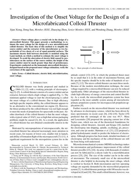
Fig. 1.<br />
Basic principle <strong>of</strong> colloid thruster.<br />
attitude control [12]–[15], in which <strong>the</strong> produced thrust must<br />
be so small that it is in <strong>the</strong> order <strong>of</strong> micrometer-Newton, and<br />
<strong>the</strong> specific impulse should be in <strong>the</strong> order <strong>of</strong> hundreds <strong>of</strong> seconds<br />
[7], [12]. The micro colloid thruster can meet <strong>the</strong>se needs.<br />
Because <strong>of</strong> <strong>the</strong> modern micr<strong>of</strong>abrication technique, <strong>the</strong> onset<br />
voltage required by a microcolloid thruster can now be reduced<br />
significantly. O<strong>the</strong>r advantages <strong>of</strong> <strong>the</strong> microcolloid thruster include<br />
high efficiency <strong>of</strong> energy conversion and control flexibility.<br />
As a result, <strong>the</strong> microcolloid propulsion system has been<br />
regarded as <strong>the</strong> most suitable system among all microelectric<br />
primary propulsion systems <strong>for</strong> microspacecraft propulsion applications<br />
[9].<br />
Fur<strong>the</strong>r research on <strong>the</strong> microcolloid thruster was motivated<br />
by advances in electrospray science, which has been driven by<br />
mass spectrometry in recent years [6], [16]–[18]. Taylor [19]<br />
predicted that <strong>the</strong> semiangle <strong>of</strong> <strong>the</strong> cone was 49.3 ◦ . Mora<br />
and Loscertales [20] proposed <strong>the</strong> spraying current law <strong>of</strong> <strong>the</strong><br />
Taylor cone, which was one <strong>of</strong> <strong>the</strong> <strong>the</strong>oretical foundations <strong>for</strong><br />
designing colloid thrusters. Jaworek and Krupa [18] clarified<br />
<strong>the</strong> electrospray into dripping, spindle, oscillating, jet, precession,<br />
and cone-jet modes. Hartman et al. [21], [22] proposed a<br />
global hydrodynamic model to predict <strong>the</strong> behavior <strong>of</strong> electrospray.<br />
Although progress has been made, detailed mechanics <strong>of</strong><br />
electrospray and <strong>the</strong> mechanics <strong>of</strong> <strong>the</strong> colloid thruster are still<br />
far from being well understood.<br />
Microelectromechanical systems (MEMS) technology makes<br />
<strong>the</strong> micromation and per<strong>for</strong>mance improvement <strong>of</strong> <strong>the</strong> colloid<br />
thruster possible [23], [24]. An array with thousands <strong>of</strong> emitters<br />
can now be fabricated in a silicon wafer by a micr<strong>of</strong>abrication<br />
process [25], [26]. The size <strong>of</strong> <strong>the</strong> emitter can be in <strong>the</strong> order<br />
<strong>of</strong> micrometer. The extremely small size <strong>of</strong> <strong>the</strong> microcolloid<br />
thruster is also helpful in decreasing <strong>the</strong> onset voltage, which<br />
is verified in Section II. Both micromation and low operating<br />
voltage are urgently demanded by <strong>the</strong> microcolloid propulsion<br />
system [7]. A colloid thruster prototype with 100 nozzles was developed<br />
in [4] and [10]. This small colloid thruster, however, was<br />
1083-4435/$20.00 © 2006 <strong>IEEE</strong>
XIONG et al.: INVESTIGATION OF THE ONSET VOLTAGE FOR THE DESIGN OF A MICROFABRICATED COLLOID THRUSTER 67<br />
Fig. 2.<br />
Typical shape <strong>of</strong> conventional colloid thrusters.<br />
Fig. 4.<br />
Electrostatic field <strong>of</strong> electrodes <strong>of</strong> microthruster.<br />
microthruster are regarded as two hyperboloids <strong>of</strong> two sheets<br />
<strong>of</strong> a set <strong>of</strong> equal potential surfaces. The maximum electric field<br />
between electrodes is derived by Lamé method, based on which<br />
a method to estimate <strong>the</strong> onset voltage is proposed. The condition<br />
to eliminate <strong>the</strong> influence <strong>of</strong> protuberances produced in micr<strong>of</strong>abrication<br />
is also discussed in this paper. Four microthrusters<br />
are designed according to <strong>the</strong> onset voltage estimation. Testing<br />
results <strong>of</strong> <strong>the</strong>se thrusters show that <strong>the</strong> proposed onset voltage<br />
estimation works effectively.<br />
Fig. 3.<br />
Surface <strong>of</strong> silicon after ICP etching.<br />
not based on <strong>the</strong> micr<strong>of</strong>abrication. Fur<strong>the</strong>r work on microcolloid<br />
thruster array was per<strong>for</strong>med by Fernando. 1 Paine [27] designed<br />
ano<strong>the</strong>r addressable microcolloid thruster array, in which a minimum<br />
thrust <strong>of</strong> 0.1 µmN was expected.<br />
It is noted that <strong>the</strong> fabrication process <strong>of</strong> a microcolloid<br />
thruster is largely different than that <strong>of</strong> a conventional thruster.<br />
To obtain <strong>the</strong> high electric field, <strong>the</strong> source emitter <strong>of</strong> <strong>the</strong> conventional<br />
colloid thruster usually employs a tapered tip [1], [2],<br />
as shown in Fig. 2. However, it is difficult to fabricate <strong>the</strong> tapered<br />
source emitter in <strong>the</strong> micr<strong>of</strong>abrication process. A typical shape<br />
<strong>of</strong> <strong>the</strong> micr<strong>of</strong>abricated source emitter looks like a hollowed<br />
cylinder with dimensions in <strong>the</strong> order <strong>of</strong> tens <strong>of</strong> micrometer,<br />
<strong>for</strong>med by deep dry etching on <strong>the</strong> silicon such as inductively<br />
coupled plasma (ICP) or deep reactive ion etching. Due to <strong>the</strong><br />
long-time deep dry etching, many protuberances exist on <strong>the</strong><br />
surface <strong>of</strong> silicon. Fig. 3 shows <strong>the</strong> surface <strong>of</strong> silicon at 40 min<br />
after ICP etching, from which 2-µm-high protuberances can be<br />
found. These protuberances may result in a serious coarseness<br />
problem.<br />
To solve problems <strong>of</strong> <strong>the</strong> electrode shape and coarseness, we<br />
need to reconsider <strong>the</strong> electric field distribution between electrodes<br />
and <strong>the</strong> onset voltage <strong>of</strong> <strong>the</strong> microcolloid thruster. This<br />
paper presents a new method <strong>for</strong> estimating <strong>the</strong> onset voltage<br />
through analyzing <strong>the</strong> surface tension stress and <strong>the</strong> <strong>for</strong>ce <strong>of</strong><br />
<strong>the</strong> electric field at <strong>the</strong> tip <strong>of</strong> <strong>the</strong> source emitter <strong>of</strong> <strong>the</strong> microcolloid<br />
thruster. The source emitter and <strong>the</strong> extractor <strong>of</strong> <strong>the</strong><br />
1 Online. Available: http://web.mit.edu/aeroastro/www/labs/SPL/Research/<br />
colloid.htm<br />
II. ONSET VOLTAGE ESTIMATION<br />
The onset voltage is estimated based on <strong>the</strong> balance between<br />
<strong>the</strong> surface tension and <strong>the</strong> <strong>for</strong>ce <strong>of</strong> <strong>the</strong> electrostatic field on <strong>the</strong><br />
surface <strong>of</strong> droplet at <strong>the</strong> tip <strong>of</strong> source emitter <strong>of</strong> a microcolloid<br />
thruster. In this section, <strong>the</strong> electrostatic field between <strong>the</strong> source<br />
emitter and <strong>the</strong> extractor <strong>of</strong> <strong>the</strong> microcolloid thruster, as well as<br />
an estimation <strong>for</strong> <strong>the</strong> onset voltage estimation, are discussed.<br />
A. Electrostatic Field Distribution<br />
The potential between electrodes <strong>of</strong> <strong>the</strong> microcolloid thruster,<br />
denoted by V, can be described in a cylindrical coordinate frame<br />
[30],i.e.,<br />
1<br />
r<br />
∂<br />
∂r<br />
(<br />
r ∂V )<br />
+ 1 ∂ 2 V<br />
∂r r 2 ∂θ 2<br />
+ ∂2 V<br />
=0 (1)<br />
∂z2 where r, θ, and z are three basic coordinates <strong>of</strong> <strong>the</strong> cylindrical<br />
coordinate system. The boundary conditions <strong>of</strong> (1) are<br />
V = V 0 (r = r 1 ,z =0)<br />
V =0 (R 1 ≤ r ≤ R 2 ,z = d + r)<br />
where r 1 is <strong>the</strong> inner radius <strong>of</strong> <strong>the</strong> source emitter, R 1 is <strong>the</strong> outer<br />
radius <strong>of</strong> <strong>the</strong> extractor, R 2 is <strong>the</strong> inner radius <strong>of</strong> <strong>the</strong> extractor,<br />
d is <strong>the</strong> distance between two electrodes, and V 0 is <strong>the</strong> applied<br />
voltage between two electrodes. Fig. 4 illustrates <strong>the</strong> electrostatic<br />
field <strong>of</strong> electrodes <strong>of</strong> <strong>the</strong> microthruster, where <strong>the</strong> origin<br />
<strong>of</strong> <strong>the</strong> inertia coordinate frame o-xyz is located in <strong>the</strong> center<br />
top <strong>of</strong> <strong>the</strong> cylinder. The droplet is supposed to be a cone with<br />
height <strong>of</strong> 2r 1 . To enhance electric field in <strong>the</strong> z direction, d ≫ r 1<br />
in <strong>the</strong> design.
68 <strong>IEEE</strong>/ASME TRANSACTIONS ON MECHATRONICS, VOL. 11, NO. 1, FEBRUARY 2006<br />
The solution <strong>of</strong> (1) is [30]<br />
∞∑<br />
V =<br />
i=0<br />
A i J 0<br />
(<br />
x i<br />
r<br />
r 1<br />
)<br />
sh<br />
(<br />
x i<br />
z<br />
r 1<br />
)<br />
where J 0 (·) is <strong>the</strong> zero-order Bessel function, and coefficients<br />
A i can be determined by <strong>the</strong> boundary conditions. Note that <strong>the</strong><br />
coefficients A i are hard to determine exactly.<br />
Equation (2) is too complicated to be used <strong>for</strong> estimation <strong>of</strong><br />
<strong>the</strong> electric field distribution between electrodes. An approximate<br />
solution <strong>of</strong> (1) is developed here, based on <strong>the</strong> Lamé<br />
method .[29]–[31] In <strong>the</strong> inertia coordinate frame o-xyz, <strong>the</strong> following<br />
equation represents a set <strong>of</strong> hyperboloids <strong>of</strong> two sheets:<br />
x 2<br />
λ + y2<br />
λ −<br />
z2<br />
c 2 = −1 (3)<br />
− λ<br />
where c denotes <strong>the</strong> distance between <strong>the</strong> focal point and <strong>the</strong><br />
origin, λ is a variable, and λ
XIONG et al.: INVESTIGATION OF THE ONSET VOLTAGE FOR THE DESIGN OF A MICROFABRICATED COLLOID THRUSTER 69<br />
where δ denotes <strong>the</strong> surface tension coefficient <strong>of</strong> <strong>the</strong> liquid<br />
cone. The electrostatic stress is<br />
P E = 1 2 ε 0E 2 (15)<br />
where ε 0 is <strong>the</strong> permittivity <strong>of</strong> vacuum. Suppose P E = P δ ,we<br />
<strong>the</strong>n have<br />
√<br />
δ<br />
E =2<br />
r 1 ε 0 tan(a) . (16)<br />
Substituting (16) into (11) yields <strong>the</strong> onset voltage<br />
√<br />
(<br />
1 √<br />
V 0 =<br />
δr1 ln 2+2 d ε 0 tan(a)<br />
r 1<br />
√ (<br />
− 2 d +1<br />
)(3+2 d ) )<br />
r 1 r 1<br />
(<br />
=0.312 × 10 6√ δr 1 ln 2+2 d r 1<br />
√ (<br />
− 2 d )(<br />
+1 3+2 d ) ) . (17)<br />
r 1 r 1<br />
Fig. 6.<br />
Meshing model <strong>of</strong> electrodes <strong>of</strong> microcolloid thruster.<br />
It can be seen from (17) that <strong>the</strong> onset voltage V 0 greatly<br />
depends on <strong>the</strong> design <strong>of</strong> <strong>the</strong> radius r 1 , via a relationship <strong>of</strong> √ r 1<br />
in <strong>the</strong> expression <strong>of</strong> V 0 . [The variation <strong>of</strong> r 1 in ln(·) has little<br />
influence to V 0 .] A small value <strong>of</strong> r 1 results in a small value <strong>of</strong><br />
V 0 directly. In conventional colloid thrusters, <strong>the</strong> radius r 1 <strong>of</strong><br />
<strong>the</strong> source emitter is in <strong>the</strong> scale <strong>of</strong> millimeter, whereas in <strong>the</strong><br />
proposed MEMS-based thruster, <strong>the</strong> radius r 1 is in <strong>the</strong> scale <strong>of</strong><br />
micrometer. This is <strong>the</strong> main reason why <strong>the</strong> onset voltage <strong>of</strong><br />
<strong>the</strong> proposed microthruster can be reduced dramatically.<br />
III. SIMULATIONS AND DISCUSSIONS<br />
A. Simulations <strong>of</strong> Electric Field<br />
To verify <strong>the</strong> electric field in (11), a comparison between<br />
results obtained by (11) and results obtained by <strong>the</strong> finite element<br />
method was per<strong>for</strong>med in simulations. The meshing model used<br />
by <strong>the</strong> finite element method is shown in Fig. 6. The units <strong>of</strong> all<br />
length variables (e.g., d and r 1 ) are micrometers. The electric<br />
field between electrodes in <strong>the</strong> z direction has <strong>the</strong> maximum<br />
value at <strong>the</strong> tip <strong>of</strong> <strong>the</strong> source emitter (as seen in Fig. 5), which<br />
has <strong>the</strong> great influence to <strong>the</strong> onset voltage. Fig. 7 illustrates<br />
<strong>the</strong> numerical solution <strong>of</strong> <strong>the</strong> electric field by <strong>the</strong> finite element<br />
method, where R 1 =30µm, R 2 =50µm, R =15µm, d =<br />
420 µm, h =80µm, V = 2000 V, and h denotes <strong>the</strong> height <strong>of</strong><br />
<strong>the</strong> source emitter (see more details in Fig. 12). It is seen that <strong>the</strong><br />
maximum value <strong>of</strong> <strong>the</strong> electric field between electrodes around<br />
<strong>the</strong> tip <strong>of</strong> <strong>the</strong> source emitter ranges between 55.2 V/µm and<br />
55.7 V/µm. By (11), <strong>the</strong> maximum electric field was estimated<br />
to be 57.26 V/µm. The results obtained by <strong>the</strong> two methods are<br />
quite similar.<br />
The same analysis was fur<strong>the</strong>r per<strong>for</strong>med when electrodes<br />
have different sizes. Results are listed in Table I, where Ea denotes<br />
<strong>the</strong> value <strong>of</strong> <strong>the</strong> maximum electric field calculated by <strong>the</strong><br />
Fig. 7.<br />
Results obtained by finite element analysis.<br />
TABLE I<br />
MAXIMUM ELECTRIC FIELD BETWEEN ELECTRODES<br />
finite element method, and Es denotes <strong>the</strong> value <strong>of</strong> <strong>the</strong> maximum<br />
electric field calculated by (11). It is seen that all values <strong>of</strong> Es<br />
are close to those <strong>of</strong> Ea, which indicates that <strong>the</strong> proposed simple<br />
electric field estimation is comparable to <strong>the</strong> finite element<br />
method. Note that <strong>the</strong> extractor is simplified as a plane when<br />
using (11), which enhances <strong>the</strong> electrical field <strong>of</strong> <strong>the</strong> source<br />
emitter. In <strong>the</strong> meshing model used by <strong>the</strong> finite element analysis,<br />
<strong>the</strong> extractor is a hollowed cylinder with <strong>the</strong> inner and outer<br />
radius. This is why Es is slightly larger than Ea in Table I.<br />
B. Influence <strong>of</strong> Aberration <strong>of</strong> Electric Field<br />
As mentioned in Section I and illustrated in Fig. 3, deep dry<br />
etch results in protuberances on <strong>the</strong> silicon surface. Heights <strong>of</strong>
70 <strong>IEEE</strong>/ASME TRANSACTIONS ON MECHATRONICS, VOL. 11, NO. 1, FEBRUARY 2006<br />
TABLE II<br />
ESTIMATED ONSET VOLTAGES<br />
Fig. 8.<br />
Model <strong>of</strong> electrodes with protuberances.<br />
To eliminate <strong>the</strong> influence <strong>of</strong> <strong>the</strong> aberration <strong>of</strong> electric field,<br />
<strong>the</strong> height <strong>of</strong> <strong>the</strong> source emitter should be more than 75 µm.<br />
There<strong>for</strong>e, we conclude that when (11) and (17) are used to<br />
design <strong>the</strong> microcolloid thruster, it is necessary to ensure <strong>the</strong><br />
height <strong>of</strong> <strong>the</strong> source emitter is great enough compared with that<br />
<strong>of</strong> protuberances. O<strong>the</strong>rwise, <strong>the</strong> aberration <strong>of</strong> <strong>the</strong> electric field<br />
caused by <strong>the</strong> protuberances has to be taken into account. Fur<strong>the</strong>r<br />
analysis has been given when H P =1µm, R P =0.5 µm, and<br />
H P =0.5 µm, and R P =0.25 µm, and it was found that <strong>the</strong><br />
values <strong>of</strong> <strong>the</strong> electric field stabilize around 55.5 V/µm at smaller<br />
values <strong>of</strong> h (i.e., 60 and 48 µm, respectively). It will be helpful<br />
to reduce <strong>the</strong> influence <strong>of</strong> <strong>the</strong> aberration <strong>of</strong> electric field induced<br />
by protuberances, if micr<strong>of</strong>abrication is improved and <strong>the</strong> height<br />
<strong>of</strong> protuberance is decreased.<br />
Fig. 9.<br />
Electric field versus height <strong>of</strong> source emitter.<br />
protuberances are not identical and increase as <strong>the</strong> ICP etching<br />
time increases. Protuberances affect <strong>the</strong> distribution <strong>of</strong> <strong>the</strong><br />
electric field between electrodes, but this influence can be eliminated<br />
if <strong>the</strong> source emitter <strong>of</strong> <strong>the</strong> microcolloid thruster is high<br />
enough. In <strong>the</strong> following, a finite element analysis model <strong>of</strong> <strong>the</strong><br />
microthruster with protuberances is developed <strong>for</strong> investigation<br />
<strong>of</strong> <strong>the</strong> relationship between <strong>the</strong> aberration <strong>of</strong> <strong>the</strong> electric field<br />
caused by protuberances and <strong>the</strong> height <strong>of</strong> <strong>the</strong> source emitter.<br />
Fig. 8 illustrates <strong>the</strong> finite element model, in which <strong>the</strong> height<br />
<strong>of</strong> <strong>the</strong> protuberance, denoted by H P ,is2µm, and <strong>the</strong> radius R P<br />
is 1 µm. The o<strong>the</strong>r parameters are R 1 =30µm, R 2 =50µm,<br />
r 1 =15µm, and d = 420 µm. For simplicity, only eight protuberances<br />
were considered in <strong>the</strong> model. These protuberances<br />
are identical in height and located in <strong>the</strong> axial symmetry<br />
positions.<br />
The relationship between <strong>the</strong> electrical field and <strong>the</strong> height<br />
<strong>of</strong> <strong>the</strong> source emitter is shown in Fig. 9. It can be seen that<br />
<strong>the</strong> maximum value <strong>of</strong> <strong>the</strong> electrical field between electrodes<br />
increases as <strong>the</strong> height <strong>of</strong> <strong>the</strong> source emitter increases. When<br />
<strong>the</strong> height <strong>of</strong> <strong>the</strong> source emitter is more than 75 µm, <strong>the</strong> value<br />
<strong>of</strong> <strong>the</strong> electric field stabilizes around 55.5 V/µm. In <strong>the</strong> case <strong>of</strong><br />
H P =2µm and R P =1µm, protuberances weaken <strong>the</strong> electric<br />
field obviously when <strong>the</strong> source emitter is shorter than 70 µm.<br />
C. <strong>Onset</strong> <strong>Voltage</strong> Estimation<br />
We now estimate <strong>the</strong> onset voltages <strong>of</strong> <strong>the</strong> microcolloid<br />
thrusters listed in Table I by (17). The onset voltage relates to <strong>the</strong><br />
surface tension coefficient <strong>of</strong> <strong>the</strong> propellant. When <strong>for</strong>mamide<br />
doped with 30% NaI in weight is used as <strong>the</strong> propellant, δ is<br />
about 0.058 N/m. Using <strong>the</strong> same parameters as in Table I, <strong>the</strong><br />
onset voltages <strong>of</strong> <strong>the</strong> microthrusters were predicted and given<br />
in Table II, where <strong>the</strong> numbers 1–4 correspond to <strong>the</strong> numbers<br />
in Table I. The values <strong>of</strong> <strong>the</strong> onset voltage in Table II are significantly<br />
smaller than those <strong>of</strong> conventional colloid thrusters.<br />
The correctness <strong>of</strong> such estimation and <strong>the</strong> design followed is<br />
verified in <strong>the</strong> experiment in Section IV.<br />
IV. EXPERIMENTS<br />
To verify <strong>the</strong> correctness <strong>of</strong> (17), four microcolloid thrusters<br />
with <strong>the</strong> same parameters as given in Table I, were fabricated and<br />
used in <strong>the</strong> tests. The thrusters were fabricated by bulk silicon<br />
process.<br />
A. Fabrication<br />
The fabrication <strong>of</strong> <strong>the</strong> microthruster includes fabrication <strong>of</strong><br />
<strong>the</strong> source emitter and <strong>the</strong> extractor, as shown in Figs. 10 and 11.<br />
The first step <strong>of</strong> <strong>the</strong> source emitter fabrication process was that<br />
50% KOH etched <strong>the</strong> silicon wafer to create a square pyramidal<br />
pit. The etching depth was about 280 µm. SiO 2 /Si 3 N 4 was used<br />
as <strong>the</strong> mask. Second, <strong>the</strong> source emitter with a cylinder shape<br />
was built by ICP. Patterned photoresist mask was used <strong>for</strong> <strong>the</strong><br />
ICP to <strong>for</strong>m a round pit with 60 µm in depth. The outer wall <strong>of</strong><br />
<strong>the</strong> source emitter was <strong>for</strong>med by <strong>the</strong> o<strong>the</strong>r ICP with aluminium<br />
layer as <strong>the</strong> mask, where <strong>the</strong> depth was 80 µm. Finally, <strong>the</strong> inner<br />
wall <strong>of</strong> <strong>the</strong> source emitter was <strong>for</strong>med, where <strong>the</strong> depth was
XIONG et al.: INVESTIGATION OF THE ONSET VOLTAGE FOR THE DESIGN OF A MICROFABRICATED COLLOID THRUSTER 71<br />
Fig. 12.<br />
SEM photo <strong>of</strong> source emitter.<br />
Fig. 10.<br />
Fabrication process steps <strong>of</strong> source.<br />
Fig. 13.<br />
SEM photo <strong>of</strong> extractor.<br />
Fig. 11.<br />
Fabrication process steps <strong>of</strong> extractor.<br />
Fig. 14.<br />
Packaged microcolloid thruster.<br />
140 µm, which was enough to make ICP penetrate through <strong>the</strong><br />
silicon wafer.<br />
The fabrication process <strong>of</strong> <strong>the</strong> extractor was relatively simple.<br />
As shown in Fig. 11, <strong>the</strong> first step was similar to that <strong>of</strong> <strong>the</strong><br />
source emitter, except that <strong>the</strong> etching depth was 360 µm. The<br />
following step was to <strong>for</strong>m <strong>the</strong> aluminium electrode, and <strong>the</strong>n<br />
ICP was used to penetrate through <strong>the</strong> silicon wafer and <strong>for</strong>m<br />
<strong>the</strong> exiting channel <strong>of</strong> <strong>the</strong> spraying droplet.<br />
Two scanning electron microscope (SEM) photos <strong>of</strong> a source<br />
emitter and an extractor are shown in Figs. 12 and 13, respectively.<br />
The height <strong>of</strong> <strong>the</strong> source emitter is about 80 µm. In<br />
Fig. 12, <strong>the</strong> protuberances are about 2 µm in height and 1 µmin<br />
width. There is a glass spacer in <strong>the</strong> middle <strong>of</strong> <strong>the</strong> source emitter<br />
and <strong>the</strong> extractor. Epoxy was used to bond <strong>the</strong> structure. Fig. 14<br />
illustrates <strong>the</strong> photo <strong>of</strong> a packaged microcolloid thruster.
72 <strong>IEEE</strong>/ASME TRANSACTIONS ON MECHATRONICS, VOL. 11, NO. 1, FEBRUARY 2006<br />
Fig. 15.<br />
Block diagram <strong>of</strong> test system.<br />
Fig. 17.<br />
Original output <strong>of</strong> displacement sensor (U =0V).<br />
Fig. 18.<br />
Output <strong>of</strong> displacement sensor after filtering (U = 1400 V).<br />
Fig. 16.<br />
Photo <strong>of</strong> test facility.<br />
TABLE III<br />
ONSET VOLTAGES IN TESTS.<br />
B. Tests<br />
Fig. 15 illustrates a testing structure used to verify <strong>the</strong> developed<br />
thruster. A cantilever beam with a thruster onboard was<br />
used as a sensor. When <strong>the</strong> <strong>for</strong>ce produced by <strong>the</strong> thruster acts<br />
on <strong>the</strong> cantilever beam, <strong>the</strong> beam deflects. The deflection was<br />
measured by a current vortex displacement sensor, which could<br />
translate <strong>the</strong> displacement into an electrical signal with a sensitivity<br />
<strong>of</strong> 8 mV/µm. The electrical signal was recorded by an<br />
A/D converter. The sensing system was placed in a high vacuum<br />
box with 10 −5 torr air pressure. Fig. 16 illustrates a photo <strong>of</strong> <strong>the</strong><br />
testing system.<br />
The output <strong>of</strong> <strong>the</strong> displacement sensor includes two parts:<br />
<strong>the</strong> displacement <strong>of</strong> <strong>the</strong> cantilever beam caused by <strong>the</strong> external<br />
<strong>for</strong>ce, and <strong>the</strong> vibration superposed on that displacement.<br />
Because <strong>the</strong> displacement is so small that is in <strong>the</strong> scale <strong>of</strong><br />
micrometer, <strong>the</strong> effect <strong>of</strong> <strong>the</strong> vibration to <strong>the</strong> output must be<br />
considered. The wave pr<strong>of</strong>ile <strong>of</strong> <strong>the</strong> free vibration is shown in<br />
Fig. 17, where <strong>the</strong> vibration amplitude is about several micrometers.<br />
Vibration analysis shows that <strong>the</strong> main components <strong>of</strong><br />
<strong>the</strong> vibration signal have frequencies <strong>of</strong> 1.95 and 13.67 Hz, respectively.<br />
To obtain <strong>the</strong> exact value <strong>of</strong> <strong>the</strong> displacement, <strong>the</strong><br />
output components with frequencies <strong>of</strong> 1.95 and 13.67 Hz were<br />
removed from <strong>the</strong> signal. After removing <strong>the</strong>se two components<br />
from Fig. 17, <strong>the</strong> displacement sensor appeared an output <strong>of</strong><br />
−3.12 V when <strong>the</strong> external <strong>for</strong>ce is zero.<br />
Experimental results show that <strong>the</strong> onset voltage <strong>of</strong> <strong>the</strong> first<br />
microthruster is about 1260 V. When <strong>the</strong> applied voltage increases<br />
from 0 to 1300 V, <strong>the</strong> cantilever beam remains balanced,<br />
as shown in Fig. 17. When <strong>the</strong> applied voltage reached<br />
1300 V, <strong>the</strong> beam began to deflect. Removing components with<br />
<strong>the</strong> first- and <strong>the</strong> second-order natural frequencies from <strong>the</strong> signal,<br />
<strong>the</strong> output <strong>of</strong> <strong>the</strong> displacement sensor is plotted in Fig. 18.<br />
Compared with <strong>the</strong> output <strong>of</strong> <strong>the</strong> displacement sensor with zero<br />
input, <strong>the</strong>re is an <strong>of</strong>fset <strong>of</strong> about 0.49 V, which implies that <strong>the</strong><br />
electrospray begins.<br />
The tests were fur<strong>the</strong>r per<strong>for</strong>med on <strong>the</strong> remaining three microthrusters.<br />
All results are listed in Table III. It can be seen<br />
that <strong>the</strong> testing results in Table III basically agree with those<br />
predicted by (17) in Table II. The slight difference is explained<br />
as follows: 1) <strong>the</strong> size <strong>of</strong> <strong>the</strong> extractor is neglected when using<br />
(17); 2) <strong>the</strong> size <strong>of</strong> <strong>the</strong> designed thruster is slightly different
XIONG et al.: INVESTIGATION OF THE ONSET VOLTAGE FOR THE DESIGN OF A MICROFABRICATED COLLOID THRUSTER 73<br />
from that <strong>of</strong> <strong>the</strong> actual one; and 3) <strong>the</strong>re is a “voltage loss” due<br />
to <strong>the</strong> interaction <strong>of</strong> <strong>the</strong> charged droplets [5].<br />
It is also verified in <strong>the</strong> test that <strong>the</strong> onset voltage <strong>of</strong> <strong>the</strong> microcolloid<br />
thruster can be reduced dramatically compared with that<br />
<strong>of</strong> conventional colloid thrusters. In our test, <strong>the</strong> microcolloid<br />
thruster could work under 1300 V, whereas <strong>the</strong> working voltage<br />
<strong>of</strong> a conventional colloid thruster is usually at least 5000–<br />
10 000 V. The advantage <strong>of</strong> <strong>the</strong> low onset voltage required by<br />
our microcolloid thruster makes it easier to be integrated with<br />
<strong>the</strong> o<strong>the</strong>r colloid system components.<br />
V. CONCLUSION<br />
This paper presents a new method to analyze <strong>the</strong> electric field<br />
distribution between <strong>the</strong> source emitter and <strong>the</strong> extractor, and<br />
an estimation <strong>of</strong> <strong>the</strong> onset voltage <strong>of</strong> <strong>the</strong> microcolloid thruster.<br />
The basic idea is to regard two electrodes as two equal potential<br />
surfaces. To avoid <strong>the</strong> aberration <strong>of</strong> <strong>the</strong> electric field caused by<br />
protuberances on <strong>the</strong> surface <strong>of</strong> <strong>the</strong> source emitter, <strong>the</strong> height<br />
<strong>of</strong> <strong>the</strong> source emitter must be great enough compared with that<br />
<strong>of</strong> protuberances. Several microcolloid thrusters are designed<br />
and fabricated based on <strong>the</strong> proposed onset voltage estimation.<br />
Testing results show that <strong>the</strong> actual onset voltages <strong>of</strong> <strong>the</strong> newly<br />
designed thrusters match <strong>the</strong> estimated values. Meanwhile, it<br />
has been shown that <strong>the</strong> micromation <strong>of</strong> <strong>the</strong> colloid thruster<br />
helps decrease <strong>the</strong> operating voltage dramatically.<br />
REFERENCES<br />
[1] A. G. Bailey and J. E. Bracher, “Capillary-fed annular colloid thruster,”<br />
J. Spacecraft Rockets, vol. 9, no. 7, pp. 518–524, 1972.<br />
[2] S. Zafran, J. C. Beynon, P. W. Kidd, H. Shelton, and F. A. Jackson, “Onemillipound<br />
colloid thruster system development,” J. Spacecraft Rockets,<br />
vol. 10, no. 8, pp. 531–533, 1973.<br />
[3] C. D. Hendricks, “Parametric studies <strong>of</strong> electrohydrodynamic spraying,”<br />
AIAA66-252, 1966.<br />
[4] P. Lozano and M. Martinez-Sanchez, “Experimental study <strong>of</strong> colloid<br />
plumes,” AIAA2001-3334, 2001.<br />
[5] M. Gamero-Castano and V. Hruby, “Electrospray as a source <strong>of</strong> nanoparticles<br />
<strong>for</strong> efficient colloid thrusters,” J. Propulsion Power, vol. 17, no. 5,<br />
pp. 977–987, 2001.<br />
[6] M. Martinez-Sanchez, J. F. de la Mora, H. M. Gamero-Castano, and<br />
V. Khayms, “Research on colloid thrusters,” presented at <strong>the</strong> 26th Int.<br />
Electric Propulsion Conf., Kitakyushu, Japan, 1999.<br />
[7] J. G. Reichbach, R. J. Sedwick, and M. Martinez-Sanchez, “Micropropulsion<br />
system selection <strong>for</strong> precision <strong>for</strong>mation flying satellites,”<br />
AIAA2001-3646, 2001.<br />
[8] S. Marcuccio, G. L. Lorenzi, and M. A. Centrospazio, “Development <strong>of</strong> a<br />
miniaturized field emission propulsion system,” AIAA98-3919, 1998.<br />
[9] J. Mueller, “Thruster options <strong>for</strong> microspacecraft: A review and evaluation<br />
<strong>of</strong> existing hardware and emerging technologies,” AIAA97-3058, 1997.<br />
[10] F. M. Pranajaya and M. A. Cappelli, “Development <strong>of</strong> a colloid<br />
micro-thruster <strong>for</strong> flight demonstration on <strong>the</strong> emerald nanosatellite,”<br />
AIAA2001-23, 2001.<br />
[11] E. Y. Choueiri, “Overview <strong>of</strong> U.S. academic programs in electric propulsion,”<br />
presented at <strong>the</strong> 35th AIAA Joint Propulsion Conf., Los Angeles,<br />
CA, Jun. 1999.<br />
[12] J. Mueller, I. Chakraborty, S. Vargo, C. Marrese, V. White, and D. Bame,<br />
“Towards micropropulsion systems on-a-chip: Initial results <strong>of</strong> component<br />
feasibility studies,” in Proc. <strong>IEEE</strong> Aerospace Conf., vol. 4, 2000, pp. 149–<br />
168.<br />
[13] V. Khayms and M. Martinez-Sanchez, “<strong>Design</strong> <strong>of</strong> a miniaturized Hall<br />
thruster <strong>for</strong> microsatellites,” AIAA96-3291, 1996.<br />
[14] M. Young and E. P. Munta, “Unique hollow cathode as a code validation<br />
experiment and candidate non-magnetic ion micro-thruster,” AIAA99-<br />
2854, 1999.<br />
[15] P. J. Turchi, I. G. Mikellides, P. G. Mikellides, and H. Kamhawi, “Optimization<br />
<strong>of</strong> pulsed plasma thrusters <strong>for</strong> microsatellite propulsion,”<br />
AIAA99-2301, 1999.<br />
[16] L. Wei, W. Baoping, G. Li, Y. Hanchun, and T. Yan, “Analysis <strong>of</strong> <strong>the</strong><br />
emission per<strong>for</strong>mance <strong>of</strong> field emitter with Laplace interpolation method,”<br />
Appl. Surf. Sci., vol. 161, pp. 1–8, 2000.<br />
[17] A. M. Ganan-Calvo, “The surface charge in electrospraying: Its nature<br />
and its universal scaling laws,” J. Aerosol Sci., vol. 30, no. 7, pp. 863–872,<br />
1999.<br />
[18] A. Jaworek and A. Krupa, “Classification <strong>of</strong> <strong>the</strong> modes <strong>of</strong> EHD spraying,”<br />
J. Aerosol Sci., vol. 30, no. 7, pp. 873–893, 1999.<br />
[19] G. I. Taylor, “Disintegration <strong>of</strong> water drops in an electric field,” Proc. R.<br />
Soc. A, vol. 3, pp. 383–397, 1964.<br />
[20] J. F. de la Mora and I. G. Loscertales, “The current emitted by highly<br />
conducting Taylor cones,” J. Fluid Mech., vol. 260, pp. 155–184, 1994.<br />
[21] P. D. Noymer and M. Garel, “Stability and atomization characteristics <strong>of</strong><br />
electrohydrodynamic jets in <strong>the</strong> cone-jet and multi-jet modes,” J. Aerosol<br />
Sci., vol. 31, no. 10, pp. 1165–1172, 2000.<br />
[22] R. P. A. Hartman, D. J. Brunner, D. M. A. Camelot, J. C. M. Marijinissen,<br />
and B. Scarlett, “Jet break-up in electrohydrodynamic atomization in <strong>the</strong><br />
cone-jet mode,” J. Aerosol Sci., vol. 31, no. 1, pp. 65–95, 2000.<br />
[23] S. W. Janson and H. Helvajian, “MEMS, microengineering and serospace<br />
systems,” presented at <strong>the</strong> AIAA Joint Propulsion Conf., 1999, Paper<br />
AIAA99-3802.<br />
[24] J. Mueller et al. “A review and applicability assessment <strong>of</strong> MEMS-Based<br />
microvalve technologies <strong>for</strong> microspacecraft propulsion, ” presented at<br />
<strong>the</strong> AIAA Joint Propulsion Conf., 1999, Paper AIAA99-2725.<br />
[25] D. H. Lewis, S. W. Janson, R. B. Cohen, and E. K. Antonsson, “Digital<br />
micropropulsion,” Sens. Actuators A, Phys., vol. 80, no. 2, pp. 143–154,<br />
2000.<br />
[26] J. Mueller, I. Chakraborty, D. Bame, W. Tang, R. Lawton, and A. Wallace,<br />
“Pro<strong>of</strong>-<strong>of</strong>-concept demonstration <strong>of</strong> a vaporizing liquid micro-thruster, ”<br />
presented at <strong>the</strong> AIAA Joint Propulsion Conf., 1998, Paper AIAA98-3924.<br />
[27] M. Paine and S. Gabriel, “A micro-fabricated colloidal thruster array, ”<br />
presented at <strong>the</strong> AIAA Joint Propulsion Conf., 2001, Paper AIAA2001-<br />
3329.<br />
[28] R. S. Elliott, “Electromagnetics: History, <strong>the</strong>ory, and applications,” in<br />
<strong>IEEE</strong> Press Series on Electromagnetic Waves. New York: <strong>IEEE</strong> Press,<br />
1991, pp. 152–165.<br />
[29] P. Moon and D. E. Spencer, Field Theory Handbook, New York:<br />
Springer, 1971.<br />
[30] G. Xie, High <strong>Voltage</strong> Electrostatic Field. Shanghai, China: Shanghai<br />
Science and Technology, 1987 (in Chinese).<br />
[31] A. Beyer and D. Kö<strong>the</strong>r, “Solution <strong>of</strong> <strong>the</strong> direct stationary current problem<br />
<strong>of</strong> a three-axial ellipsoid,” Arch. Elecktrotechnik, vol. 71, pp. 131–137,<br />
1988.<br />
Jijun Xiong received <strong>the</strong> B.S. and M.S. degrees from<br />
<strong>the</strong> North China Institute <strong>of</strong> Technology in Shanxi,<br />
China, in 1993 and 1998, respectively, both in electrical<br />
engineering. He received <strong>the</strong> Ph.D. degree from<br />
Tsinghua University, Beijing, China, in 2003.<br />
From 2002 to 2003, he was a Research Assistant<br />
with <strong>the</strong> Department <strong>of</strong> Manufacturing Engineering<br />
and Engineering Management at <strong>the</strong> City University<br />
<strong>of</strong> Hong Kong, Kowloon, Hong Kong, China. He was<br />
an Associate Pr<strong>of</strong>essor in <strong>the</strong> Department <strong>of</strong> Electrical<br />
Engineering <strong>of</strong> <strong>the</strong> North University <strong>of</strong> China. He<br />
is currently with <strong>the</strong> Key Laboratory <strong>of</strong> <strong>the</strong> State Education Ministry on Instrumentation<br />
Science and Dynamic Measurement, North University <strong>of</strong> China,<br />
Shan’xi, China. His recent research interests lie in <strong>the</strong> fields <strong>of</strong> measurement<br />
and MEMS.<br />
Dong Sun (S’95–M’00) received <strong>the</strong> B.Sc. and M.Sc.<br />
degrees from Tsinghua University, Beijing, China, in<br />
1990 and 1994, respectively, both in mechatronics.<br />
He received <strong>the</strong> Ph.D. degree in robotics and automation<br />
from <strong>the</strong> Chinese University <strong>of</strong> Hong Kong,<br />
Hong Kong, in 1997.<br />
He was a Postdoctoral Researcher with <strong>the</strong> University<br />
<strong>of</strong> Toronto and a Research and Development Engineer<br />
with Ontario Industry. Since 2000, he has been<br />
with <strong>the</strong> Department <strong>of</strong> Manufacturing Engineering<br />
and Engineering Management at <strong>the</strong> City University
74 <strong>IEEE</strong>/ASME TRANSACTIONS ON MECHATRONICS, VOL. 11, NO. 1, FEBRUARY 2006<br />
<strong>of</strong> Hong Kong, Kowloon, Hong, Kong, China, where he is now an Associate<br />
Pr<strong>of</strong>essor. He is also an Adjunct Pr<strong>of</strong>essor at <strong>the</strong> University <strong>of</strong> Toronto. His<br />
research interests lie in robotics and automation, motion controls, and mechatronics.<br />
Dr. Sun is a Pr<strong>of</strong>essional Engineer in <strong>the</strong> Province <strong>of</strong> Ontario, Canada.<br />
Since 2004, he has served as an Associate Editor <strong>for</strong> <strong>IEEE</strong> TRANSACTIONS ON<br />
ROBOTICS.<br />
He is an Editor <strong>of</strong> <strong>the</strong> International Journal <strong>of</strong> Micromechatronics and Sensors<br />
and Actuators A: Physical. He also serves as Vice President <strong>of</strong> <strong>the</strong> China<br />
Instrument Society. He has received 30 patents, three national awards, and ten<br />
Ministry Awards <strong>of</strong> Science and Technology Invention and Achievement.<br />
Zhaoying Zhou (SM’02) graduated from <strong>the</strong> Department<br />
<strong>of</strong> Precision Instruments <strong>of</strong> Tsinghua University,<br />
Beijing, China, in 1961.<br />
From 1979 to 1981, he was a Visiting Scientist<br />
at <strong>the</strong> Department <strong>of</strong> Automatic Control <strong>of</strong> Lund<br />
University, Lund, Sweden. He is currently a Pr<strong>of</strong>essor<br />
in <strong>the</strong> Department <strong>of</strong> Precision Instruments<br />
and Mechanology and Chairman <strong>of</strong> <strong>the</strong> Academic<br />
Committee <strong>of</strong> <strong>the</strong> Micro/Nano Technology Research<br />
Center, Tsinghua University, Beijing, China. He has<br />
published more than 300 scientific and technical papers.<br />
His recent research interests lie in <strong>the</strong> fields <strong>of</strong> measurement, control, and<br />
micro/nano technology.<br />
Wendong Zhang (M’02) received <strong>the</strong> Ph.D. degree<br />
from Beijing Institute <strong>of</strong> Technology, Beijing, China,<br />
in 1995.<br />
From 1996 to 1998, he was a Postdoctoral Researcher<br />
at Tsinghua University, Beijing, China.<br />
From 1998 to 2001, he conducted his research at<br />
<strong>the</strong> University <strong>of</strong> Cali<strong>for</strong>nia at Berkeley and at <strong>the</strong><br />
National Measurement Laboratory, Japan. He is currently<br />
<strong>the</strong> President <strong>of</strong> North University <strong>of</strong> China,<br />
Shan’xi, China, where he is also with <strong>the</strong> Key Laboratory<br />
<strong>of</strong> <strong>the</strong> State Education Ministry on Instrumentation<br />
Science and Dynamic Measurement. His recent research interests lie in<br />
<strong>the</strong> fields <strong>of</strong> instrumentation science and MEMS.


