STK402-070 - Audio Lab of Ga
STK402-070 - Audio Lab of Ga
STK402-070 - Audio Lab of Ga

You also want an ePaper? Increase the reach of your titles
YUMPU automatically turns print PDFs into web optimized ePapers that Google loves.
Ordering number : ENN7047<br />
Thick-Film Hybrid IC<br />
<strong>STK402</strong>-<strong>070</strong><br />
Two-Channel Class AB <strong>Audio</strong> Power Amplifier IC<br />
40W + 40W<br />
Overview<br />
The <strong>STK402</strong>-000 series products are audio power<br />
amplifier hybrid ICs that consist <strong>of</strong> optimally-designed<br />
discrete component power amplifier circuits that have<br />
been miniaturized using SANYO's unique insulated metal<br />
substrate technology (IMST). SANYO has adopted a new<br />
low thermal resistance substrate in these products to<br />
reduce the package size by about 60% as compared to the<br />
earlier SANYO STK407-000 series.<br />
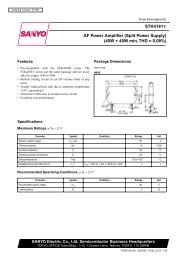
Features<br />
Package Dimensions<br />
unit: mm<br />
4189-SIP15<br />
[<strong>STK402</strong>-<strong>070</strong>]<br />
• Series <strong>of</strong> pin compatible power amplifiers ranging from<br />
20 W × 2 channels to 120 W × 2 channel (10%/1 kHz)<br />
devices. The same printed circuit board can be used<br />
depending on the output power grade.<br />
• The pin arrangement is compatible with that <strong>of</strong> the 3-<br />
channel <strong>STK402</strong>-200 series. This means that 3-channel<br />
printed circuit boards can also be used for 2-channel<br />
products.<br />
• Miniature packages<br />
— 15 W/ch to 40 W/ch (THD = 0.4%, f = 20 Hz to<br />
20 kHz); 46.6 mm × 25.5 mm × 8.5 mm *<br />
— 50 W/ch to 80 W/ch (THD = 0.4%, f = 20 Hz to<br />
20 kHz); 59.2 mm × 31.0 mm × 8.5 mm *<br />
*: Not including the pins.<br />
• Output load impedance: R L = 6 Ω<br />
• Allowable load shorted time: 0.3 seconds<br />
• Supports the use <strong>of</strong> standby, muting, and load shorting<br />
protection circuits.<br />
SANYO: SIP15<br />
Any and all SANYO products described or contained herein do not have specifications that can handle<br />
applications that require extremely high levels <strong>of</strong> reliability, such as life-support systems, aircraft’s<br />
control systems, or other applications whose failure can be reasonably expected to result in serious<br />
physical and/or material damage. Consult with your SANYO representative nearest you before using<br />
any SANYO products described or contained herein in such applications.<br />
SANYO assumes no responsibility for equipment failures that result from using products at values that<br />
exceed, even momentarily, rated values (such as maximum ratings, operating condition ranges, or other<br />
parameters) listed in products specifications <strong>of</strong> any and all SANYO products described or contained<br />
herein.<br />
SANYO Electric Co.,Ltd. Semiconductor Company<br />
TOKYO OFFICE Tokyo Bldg., 1-10, 1 Chome, Ueno, Taito-ku, TOKYO, 110-8534 JAPAN<br />
92801RM (OT) No. 7047-1/6
Series Organization<br />
<strong>STK402</strong>-<strong>070</strong><br />
These products are organized as a series based on their output capacity.<br />
Type No.<br />
Item<br />
<strong>STK402</strong>-020 <strong>STK402</strong>-030 <strong>STK402</strong>-040 <strong>STK402</strong>-050 <strong>STK402</strong>-<strong>070</strong> <strong>STK402</strong>-090 <strong>STK402</strong>-100 <strong>STK402</strong>-120<br />
Output 1 (10%/1 kHz) 20 W + 20 W 30 W + 30 W 40 W + 40 W 45 W +45 W 60 W + 60 W 80 W + 80 W 100 W + 100 W 120 W + 120 W<br />
Output 2 (0.4%/20 Hz to 20 kHz) 15 W + 15 W 20 W + 20 W 25 W + 25 W 30 W + 30 W 40 W + 40 W 50 W + 50 W 60 W + 60 W 80 W + 80 W<br />
Maximum supply voltage<br />
(No signal)<br />
±30 V ±34 V ±38 V ±40 V ±50 V ±54 V ±57 V ±65 V<br />
Maximum supply voltage<br />
(6 Ω)<br />
±28 V ±32 V ±36 V ±38 V ±44 V ±47 V ±50 V ±57 V<br />
Recommended supply voltage<br />
(6 Ω)<br />
±19 V ±22 V ±25 V ±26.5 V ±30 V ±32 V ±35 V ±39 V<br />
Package 46.6 mm × 25.5 mm × 8.5 mm 59.2 mm × 31.0 mm × 8.5 mm<br />
Specifications<br />
Maximum Ratings at Ta = 25°C<br />
Parameter Symbol Conditions Ratings Unit<br />
Maximum supply voltage (No signal) V CC max(0) ±50 V<br />
Maximum supply voltage V CC max(1) R L = 6 Ω ±44 V<br />
Thermal resistance θj-c Per power transistor 3.2 °C/W<br />
Junction temperature<br />
Tj max<br />
150 °C<br />
Both the Tj max and the Tc max conditions must be met.<br />
Operating IC substrate temperature Tc max 125 °C<br />
Storage temperature Tstg –30 to +125 °C<br />
Allowable load shorted time ts V CC = ±30.0 V, R L = 6 Ω, f = 50 Hz, P O = 40 W 0.3 s<br />
Operating Characteristics at Ta = 25°C, R L = 6 Ω (noninductive load), Rg = 600 Ω, VG = 30 dB<br />
Conditions* 1<br />
Ratings<br />
Parameter<br />
Symbol<br />
V CC (V) f (Hz) P O (W) THD (%) min typ max<br />
Output power P O (1) ±30.0 20 to 20 k 0.4 38 40<br />
(continuous output) P O (2) ±30.0 1 k 10 60<br />
Total harmonic distortion<br />
THD (1) ±30.0 20 to 20 k 1.0 VG = 30 dB 0.4<br />
THD (2) ±30.0 1 k 5.0 VG = 30 dB 0.01<br />
%<br />
Frequency characteristics f L , f H ±30.0 1.0 +0 –3 dB 20 to 50 k Hz<br />
Input impedance ri ±30.0 1 k 1.0 55 kΩ<br />
Output noise voltage *2 V NO ±36.0 Rg = 2.2 kΩ 1.2 mVrms<br />
Quiescent current I CCO ±36.0 10 40 80 mA<br />
Neutral voltage V N ±36.0 –70 0 +70 mV<br />
Notes: 1. Unless otherwise noted, use a constant-voltage supply for the power supply used during inspection.<br />
2. The output noise voltage values shown are peak values read with a VTVM. However, an AC stabilized (50 Hz) power supply should be used to<br />
minimize the influence <strong>of</strong> AC primary side flicker noise on the reading.<br />
Use the transformer power supply circuit stipulated in the figure below for output noise voltage measurement.<br />
3. Use the transformer power supply circuit stipulated in the figure below for allowable load shorted time measurement.<br />
Unit<br />
W<br />
DBA40C 10000µF<br />
+V CC<br />
500Ω<br />
500Ω<br />
--V CC<br />
10000µF<br />
Stipulated Transformer Power Supply (MG-200 equivalent)<br />
No. 7047-2/6
4.7Ω<br />
4.7Ω<br />
33µF<br />
100µF<br />
10µF<br />
10µF<br />
100µF<br />
33µF<br />
56kΩ<br />
1.8kΩ<br />
1.8kΩ<br />
56kΩ<br />
10kΩ<br />
0.22Ω<br />
0.22Ω<br />
0.22Ω<br />
0.22Ω<br />
<strong>STK402</strong>-<strong>070</strong><br />
Internal Equivalent Circuit<br />
8<br />
4<br />
R1<br />
TR7<br />
TR9<br />
R13<br />
C1<br />
TR4<br />
R6<br />
TR11<br />
R8<br />
C2<br />
1<br />
TR1<br />
TR2<br />
R3<br />
TR5<br />
TR12<br />
R11<br />
TR14<br />
TR15<br />
2<br />
R4<br />
TR8<br />
TR10<br />
R12<br />
TR3<br />
R5<br />
TR6<br />
TR13<br />
R10<br />
TR16<br />
R2<br />
D1<br />
R7<br />
R9<br />
R14<br />
13<br />
9<br />
SUB<br />
5 12 7 6<br />
10<br />
11<br />
14 15<br />
Sample Application Circuit<br />
Ch.1<br />
Ch.2<br />
Ch.1<br />
IN<br />
Ch.1<br />
NF<br />
Pre<br />
Ch.1<br />
+V CC BIAS +VE<br />
Ch.1<br />
-VE +V CC -V CC<br />
Ch.2<br />
+VE<br />
SUB<br />
Ch.2 Pre<br />
-VE -V CC<br />
SUB<br />
GND<br />
Ch.2<br />
NF<br />
1 2 4 5 6 7 8 9 10 11 12 13 14 15<br />
Ch.2<br />
IN<br />
Ch.1 IN<br />
1kΩ<br />
2.2µF<br />
470pF<br />
220pF<br />
3pF<br />
3pF<br />
220pF 2.2µF 1kΩ<br />
470pF<br />
Ch.2 IN<br />
56kΩ<br />
56kΩ<br />
100Ω<br />
100Ω<br />
3µH<br />
3µH<br />
Ch.1 OUT<br />
0.1µF<br />
4.7Ω<br />
4.7Ω<br />
0.1µF<br />
Ch.2 OUT<br />
+V CC<br />
-V CC<br />
No. 7047-3/6
<strong>STK402</strong>-<strong>070</strong><br />
Thermal Design Example<br />
The thermal resistance, θc-a <strong>of</strong> the required heat sink for the power dissipation, Pd, within the hybrid IC is determined as<br />
follows.<br />
Condition 1: The IC substrate temperature, Tc, must not exceed 125°C.<br />
Pd × θc – a + Ta < 125°C .........(1)<br />
Ta: Guaranteed ambient temperature for the end product.<br />
Condition 2: The junction temperature, Tj, <strong>of</strong> each power transistor must not exceed 150°C.<br />
Pd × θc – a + Pd/N × θj – c + Ta < 150°C .........(2)<br />
N: Number <strong>of</strong> power transistors<br />
θc-a: Thermal resistance per power transistor<br />
However, the power dissipation, Pd, for the power transistors shall be allocated equally among the N transistors.<br />
The following inequalities results from solving equations (1) and (2) for θc-a.<br />
θc – a < (125 – Ta) /Pd ..................(1)’<br />
θc – a < (150 – Ta) /Pd – θj – c/N .........(2)’<br />
Values that satisfy these two inequalities at the same time represent the required heat sink thermal resistance.<br />
When the following specifications have been stipulated, the required heat sink thermal resistance can be determined from<br />
formulas (1)’ and (2)’.<br />
• Supply voltage — V CC<br />
• Load resistance value — RL<br />
• Guaranteed ambient temperature — Ta<br />
[Example]<br />
When the IC supply voltage, V CC , is ±30 V and R L is 6 Ω, the IC internal power dissipation, Pd, will be a maximum <strong>of</strong><br />
63 W for a continuous sine wave signal at 1 kHz, according to the Pd – P O characteristics.<br />
For the music signals normally handled by audio amplifiers, a value <strong>of</strong> 1/8 P O max is generally used for Pd as an estimate<br />
<strong>of</strong> the power dissipation based on this type <strong>of</strong> continuous signal. (Note that the factor used may differ depending on the<br />
safety standards used.)<br />
That is:<br />
Pd = 42 W (When 1/8 P O max = 5 W)<br />
The number <strong>of</strong> power transistors in the audio amplifier block <strong>of</strong> these hybrid ICs, N, is 4, and the thermal resistance per<br />
transistor is 3.2°C/W. Therefore, the required heat sink thermal resistance for a guaranteed ambient temperature <strong>of</strong> 50°C<br />
will be as follows.<br />
From formula (1)’ θc – a < (125 – 50) /42<br />
< 1.78<br />
From formula (2)’ θc – a < (150 – 50) /42 – 3.2/4<br />
< 1.58<br />
Therefore, 1.58°C/W is the required heat sink thermal resistance.<br />
Note that this thermal design example assumes the use <strong>of</strong> a constant-voltage power supply, and is therefore not a verified<br />
design for any particular user's end product.<br />
No. 7047-4/6
<strong>STK402</strong>-<strong>070</strong><br />
Total device power dissipation, Pd — W<br />
Total current consumption, ICCO / ch — A<br />
Output power, PO — W<br />
80<br />
70<br />
60<br />
50<br />
40<br />
30<br />
20<br />
10<br />
0<br />
0.1<br />
1.6<br />
1.4<br />
1.2<br />
1.0<br />
0.8<br />
0.6<br />
0.4<br />
0.2<br />
0<br />
0.1<br />
100<br />
90<br />
80<br />
70<br />
60<br />
50<br />
40<br />
30<br />
V CC =±30V<br />
R L =6Ω<br />
f=1kHz<br />
VG=30dB<br />
Rg=600Ω<br />
2ch drive<br />
(same output rating)<br />
Pd — P O<br />
THD — P O<br />
7 2 3 5 7 1.0 2 3 5 7 10 2 3 5 7 100<br />
0.1<br />
1.0<br />
Output power per channel, P O / ch — W ITF02132<br />
Output power, P O — W<br />
I CCO — P O<br />
P O — f<br />
2 3 5 7 1.0 2 3 5 7 2 3 5 10 100<br />
1k<br />
80<br />
70 R L =6Ω, V CC =±30V, THD=10%<br />
60<br />
R L =6Ω, V CC =±30V, THD=0.4%<br />
50<br />
40<br />
30<br />
20<br />
10<br />
0<br />
10<br />
Output power per channel, P O / ch — W<br />
100<br />
ITF02134<br />
Frequency, f — Hz<br />
P O — V CC<br />
R L =6Ω<br />
f=1kHz<br />
Rg=600Ω<br />
1ch drive<br />
Tc=25°C<br />
f=1kHz<br />
VG=30dB<br />
R L =6Ω<br />
Rg=600Ω<br />
2ch drive<br />
THD=10%<br />
THD=0.4%<br />
Total harmonic distortion, THD — %<br />
Output power, PO — W<br />
10<br />
75<br />
3<br />
2<br />
1.0<br />
75<br />
3<br />
2<br />
0.1<br />
75<br />
3<br />
2<br />
0.01<br />
75<br />
3<br />
2<br />
0.001<br />
Tc=25°C<br />
V CC =±30V<br />
VG=30dB<br />
R L =6Ω<br />
Rg=600Ω<br />
20kH<br />
1kHz<br />
20Hz<br />
2 3 5 7 2 3 5 7 10 2 3 5 7 100<br />
ITF02133<br />
Tc=25°C<br />
VG=30dB<br />
Rg=600Ω<br />
2 3 5 7 2 3 5 7 2 3 5 710k<br />
2 3 5 7100k<br />
ITF02135<br />
20<br />
10<br />
0<br />
16 18 20 22 24 26 28 30 32 34 36<br />
Supply voltage, V CC — V ITF02136<br />
No. 7047-5/6
<strong>STK402</strong>-<strong>070</strong><br />
Specifications <strong>of</strong> any and all SANYO products described or contained herein stipulate the performance,<br />
characteristics, and functions <strong>of</strong> the described products in the independent state, and are not guarantees<br />
<strong>of</strong> the performance, characteristics, and functions <strong>of</strong> the described products as mounted in the customer’s<br />
products or equipment. To verify symptoms and states that cannot be evaluated in an independent device,<br />
the customer should always evaluate and test devices mounted in the customer’s products or equipment.<br />
SANYO Electric Co., Ltd. strives to supply high-quality high-reliability products. However, any and all<br />
semiconductor products fail with some probability. It is possible that these probabilistic failures could<br />
give rise to accidents or events that could endanger human lives, that could give rise to smoke or fire,<br />
or that could cause damage to other property. When designing equipment, adopt safety measures so<br />
that these kinds <strong>of</strong> accidents or events cannot occur. Such measures include but are not limited to protective<br />
circuits and error prevention circuits for safe design, redundant design, and structural design.<br />
In the event that any or all SANYO products (including technical data, services) described or contained<br />
herein are controlled under any <strong>of</strong> applicable local export control laws and regulations, such products must<br />
not be exported without obtaining the export license from the authorities concerned in accordance with the<br />
above law.<br />
No part <strong>of</strong> this publication may be reproduced or transmitted in any form or by any means, electronic or<br />
mechanical, including photocopying and recording, or any information storage or retrieval system,<br />
or otherwise, without the prior written permission <strong>of</strong> SANYO Electric Co., Ltd.<br />
Any and all information described or contained herein are subject to change without notice due to<br />
product/technology improvement, etc. When designing equipment, refer to the “Delivery Specification”<br />
for the SANYO product that you intend to use.<br />
Information (including circuit diagrams and circuit parameters) herein is for example only; it is not<br />
guaranteed for volume production. SANYO believes information herein is accurate and reliable, but<br />
no guarantees are made or implied regarding its use or any infringements <strong>of</strong> intellectual property rights<br />
or other rights <strong>of</strong> third parties.<br />
This catalog provides information as <strong>of</strong> September, 2001. Specifications and information herein are<br />
subject to change without notice.<br />
PS No. 7047-6/6