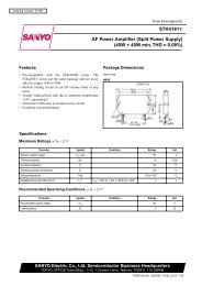
TDA7375 - Laro
TDA7375 - Laro
TDA7375 - Laro

Create successful ePaper yourself
Turn your PDF publications into a flip-book with our unique Google optimized e-Paper software.
<strong>TDA7375</strong><br />
Figure 28. Waveforms<br />
Figure 29.<br />
5.9 PCB-LAYOUT GROUNDING (general rules)<br />
The device has 2 distinct ground leads, P-GND (POWER GROUND) and S-GND (SIGNAL GROUND)<br />
which are practically disconnected from each other at chip level. Proper operation requires that P-GND<br />
and S-GND leads be connected together on the PCB-layout by means of reasonably low-resistance<br />
tracks.<br />
As for the PCB-ground configuration, a star-like arrangement whose center is represented by the supplyfiltering<br />
electrolytic capacitor ground is highly advisable. In such context, at least 2 separate paths have<br />
to be provided, one for P-GND and one for S-GND. The correct ground assignments are as follows:<br />
STANDBY CAPACITOR, pin 7 (or any other standby driving networks): on S-GND<br />
SVR CAPACITOR (pin 6): on S-GND and to be placed as close as possible to the device.<br />
INPUT SIGNAL GROUND (from active/passive signal processor stages): on S-GND.<br />
SUPPLY FILTERING CAPACITORS (pins 3,13): on P-GND.<br />
The (-) terminal of the electrolytic capacitor has to be directly tied to the battery (-) line and this should<br />
represent the starting point for all the ground paths.<br />
12/15