Current-mode PWM controller
Current-mode PWM controller
Current-mode PWM controller

Create successful ePaper yourself
Turn your PDF publications into a flip-book with our unique Google optimized e-Paper software.
Philips Semiconductors Linear Products<br />
Product specification<br />
<strong>Current</strong>-<strong>mode</strong> <strong>PWM</strong> <strong>controller</strong><br />
UC3842<br />
DESCRIPTION<br />
The UC3842 is available in an 8-Pin mini-DIP the necessary<br />
features to implement off-line, fixed-frequency current-<strong>mode</strong> control<br />
schemes with a minimal external parts count. This technique results<br />
in improved line regulation, enhanced load response characteristics,<br />
and a simpler, easier to design control loop. Topological advantages<br />
include inherent pulse-by-pulse current limiting.<br />
Protection circuitry includes built-in undervoltage lock-out and<br />
current limiting. Other features include fully-latched operation, a 1%<br />
trimmed bandgap reference, and start-up current less than 1mA.<br />
These devices feature a totem-pole output designed to source and<br />
sink high peak current from a capacitive load, such as the gate of a<br />
power MOSFET. Consistent with N-channel power devices, the<br />
output is low in the OFF-state.<br />
FEATURES<br />
• Low start-up current (≤1mA)<br />
• Automatic feed-forward compensation<br />
• Pulse-by-pulse current limiting<br />
• Enhanced load response characteristics<br />
• Undervoltage lock-out with hysteresis<br />
• Double pulse suppression<br />
• High current totem-pole output<br />
• Internally-trimmed bandgap reference<br />
• 400kHz operation, guaranteed min<br />
PIN CONFIGURATIONS<br />
COMP<br />
V FB<br />
I SENSE<br />
R T /C T<br />
COMP<br />
NC<br />
V FB<br />
NC<br />
I SENSE<br />
NC<br />
R T /C T<br />
1<br />
2<br />
3<br />
N Package<br />
4 5<br />
1<br />
2<br />
3<br />
4<br />
5<br />
6<br />
TOP VIEW<br />
D Package<br />
8<br />
7<br />
6<br />
14<br />
13<br />
12<br />
11<br />
10<br />
9<br />
7 8<br />
TOP VIEW<br />
APPLICATIONS<br />
• Off-line switched <strong>mode</strong> power supplies<br />
• DC-to-DC converters UC3842<br />
V REF<br />
V CC<br />
OUTPUT<br />
GROUND<br />
V REF<br />
NC<br />
V CC<br />
V C<br />
OUTPUT<br />
GROUND<br />
POWER GROUND<br />
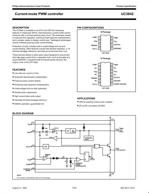
BLOCK DIAGRAM<br />
7(11)<br />
(12)7<br />
V CC<br />
GND<br />
(9)5<br />
34V<br />
16V<br />
UVLO<br />
6V<br />
S/R<br />
5V<br />
REF<br />
8(14)<br />
V REF<br />
5.0V<br />
50mA<br />
2.5V<br />
INTERNAL<br />
BIAS<br />
R T /C T<br />
(7)4<br />
OSC<br />
6(10)<br />
OUTPUT<br />
V FB<br />
COMP<br />
CURRENT<br />
SENSE<br />
(3)2<br />
(1)1<br />
(5)3<br />
ERROR<br />
AMP<br />
+<br />
–<br />
2R<br />
R<br />
1V<br />
S<br />
R<br />
CURRENT<br />
SENSE<br />
COMPARATOR<br />
<strong>PWM</strong><br />
LATCH<br />
NOTE:<br />
Pin numbers in parentheses refer to the D package.<br />
5(8)<br />
August 31, 1994 1100<br />
853-0614 13721
Philips Semiconductors Linear Products<br />
<strong>Current</strong>-<strong>mode</strong> <strong>PWM</strong> <strong>controller</strong><br />
Product specification<br />
UC3842<br />
ORDERING INFORMATION<br />
DESCRIPTION TEMPERATURE RANGE ORDER CODE DWG #<br />
8-Pin Plastic Dual In-Line Package (DIP) 0 to +70°C UC3842N 0404B<br />
14-Pin Plastic Small Outline (SO) Package 0 to +70°C UC3842D 0405B<br />
ABSOLUTE MAXIMUM RATINGS 1<br />
SYMBOL PARAMETER RATING UNIT<br />
V CC Supply voltage (I CC 70°C) 2<br />
T STG Storage temperature range -65 to +150 °C<br />
T SOLD<br />
Lead temperature<br />
(soldering, 10sec max)<br />
NOTES:<br />
1. All voltages are with respect to Pin 5; all currents are positive into the specified terminal.<br />
2. See section in application note on “Power Dissipation Calculation”.<br />
3. This parameter is guaranteed, but not 100% tested in production.<br />
300 °C<br />
August 31, 1994 1101
Philips Semiconductors Linear Products<br />
<strong>Current</strong>-<strong>mode</strong> <strong>PWM</strong> <strong>controller</strong><br />
Product specification<br />
UC3842<br />
DC AND AC ELECTRICAL CHARACTERISTICS<br />
0≤T J ≤70°C for UC3842; V CC =15V; R T =10kW; C T =3.3nF, unless otherwise specified.<br />
SYMBOL PARAMETER TEST CONDITIONS<br />
Reference section<br />
UC3842<br />
Min Typ Max<br />
V OUT Output voltage T J =25°C, I O =1mA 4.90 5.00 5.10 V<br />
Line regulation 12≤V IN ≤25V 6 20 mV<br />
Load regulation 1≤I O ≤20mA 6 25 mV<br />
UNIT<br />
Temp. stability 1 0.2 0.4 mV/°C<br />
Total output variation 1 Line, load, temp. 4.82 5.18 V<br />
V NOISE Output noise voltage 1 10Hz≤f≤10kHz, T J =25°C 50 µV<br />
Oscillator section<br />
Error amp section<br />
Long-term stability 1 T J =125°C, 1000 Hrs. 5 25 mV<br />
Output short-circuit T J =25 -30 -100 -130 mA<br />
Output short-circuit -55
Philips Semiconductors Linear Products<br />
<strong>Current</strong>-<strong>mode</strong> <strong>PWM</strong> <strong>controller</strong><br />
Product specification<br />
UC3842<br />
DC AND AC ELECTRICAL CHARACTERISTICS<br />
0≤T J ≤70°C for UC3842; V CC =15 4 ; R T =10kΩ; C T =3.3nF, unless otherwise specified<br />
SYMBOL PARAMETER TEST CONDITIONS<br />
Output section<br />
V OL<br />
V OH<br />
Output Low-Level<br />
Output High-Level<br />
UC3842<br />
Min Typ Max<br />
I SINK =20mA 0.1 0.4<br />
I SINK =200mA 1.5 2.2<br />
I SOURCE =20mA 13 13.5<br />
I SOURCE =200mA 12 13.5<br />
t R Rise time C L =1nF 50 150 ns<br />
t F Fall time C L =1nF 50 150 ns<br />
Undervoltage lockout section<br />
<strong>PWM</strong> section<br />
Start threshold 14.5 16 17.5 V<br />
Min. operating voltage after turn on 8.5 10 11.5 V<br />
Maximum duty cycle 93 97 100<br />
Minimum duty cycle 0<br />
Total standby current<br />
Start-up current 0.5 1 mA<br />
I CC Operating supply current V PIN 2 =V PIN 3 =0V 11 17 mA<br />
V CC zener voltage I CC =25mA 34 V<br />
Maximum operating frequency section<br />
Maximum operating frequency for all<br />
functions operating cycle-by-cycle<br />
NOTES:<br />
1. These parameters, although guaranteed, are not 100% tested in production.<br />
2. Parameter measured at trip point of latch with V PIN 2 =0.<br />
3. Gain defined as:<br />
A V PIN 1<br />
; 0 V<br />
V PIN 3 0.8V<br />
PIN 3<br />
UNIT<br />
V<br />
V<br />
%<br />
400 kHz<br />
UNDERVOLTAGE LOCKOUT<br />
ERROR AMP CONFIGURATION<br />
V CC<br />
7<br />
ON/OFF COMMAND<br />
TO REST OF IC<br />
2.5V<br />
+<br />
0.5mA<br />
I CC<br />
V ON<br />
V OFF<br />
UC3842<br />
16V<br />
10V<br />
Z I<br />
NOTE:<br />
Error AMP can source or sink up to 0.5mA.<br />
2<br />
V FB<br />
1<br />
COMP<br />
–<br />
Philips Semiconductors Linear Products<br />
Product specification<br />
<strong>Current</strong>-<strong>mode</strong> <strong>PWM</strong> <strong>controller</strong><br />
UC3842<br />
CURRENT SENSE CIRCUIT<br />
I S<br />
COMP<br />
1<br />
ERROR<br />
AMP<br />
2R<br />
R<br />
1V<br />
CURRENT<br />
SENSE<br />
COMPARATOR<br />
R S<br />
R<br />
3<br />
CURRENT<br />
SENSE<br />
5<br />
GND<br />
NOTE:<br />
Peak current (I S ) is determined by the formula:<br />
I S<br />
MAX 1.0V<br />
R s<br />
A small RC filter may be required to suppress switch transients.<br />
TYPICAL PERFORMANCE CHARACTERISTICS<br />
SATURATION VOLTAGE (V)<br />
Output Saturation Characteristics<br />
4<br />
3<br />
2<br />
1<br />
0<br />
0.01 0.03 0.05 0.1 0.3 0.5 1.0<br />
OUTPUT CURRENT, SOURCE OR SINK (A)<br />
VOLTAGE GAIN (dB)<br />
100<br />
Error Amplifier Open-Loop<br />
Frequency Response<br />
45<br />
80<br />
0<br />
0<br />
Av<br />
60<br />
–45<br />
40<br />
–90<br />
20<br />
–135<br />
0<br />
–180<br />
–20 –225<br />
10 100 1k 10k 100k 1M 10M<br />
FREQUENCY (Hz)<br />
PHASE (DEG)<br />
August 31, 1994 1104
Philips Semiconductors Linear Products<br />
<strong>Current</strong>-<strong>mode</strong> <strong>PWM</strong> <strong>controller</strong><br />
Product specification<br />
UC3842<br />
OPEN-LOOP LABORATORY TEST FIXTURE<br />
V REF<br />
R T<br />
A<br />
V CC<br />
4.7k<br />
2N2222<br />
100k<br />
1<br />
COMP<br />
UC3842<br />
8<br />
V REF<br />
0.1µF<br />
ERROR AMP<br />
ADJUST<br />
4.7k<br />
5k<br />
I SENSE<br />
ADJUST<br />
2<br />
V FB<br />
3<br />
I SENSE<br />
4<br />
R T /C T<br />
7<br />
V CC<br />
6<br />
OUTPUT<br />
5<br />
GND<br />
0.1µF<br />
1k<br />
1W<br />
OUTPUT<br />
C T<br />
NOTE:<br />
High peak currents associated with capacitive loads necessitate careful grounding techniques. Timing and bypass capacitors should be connected close to Pin 5 in a single point<br />
ground. The transistor and 5k potentiometer are used to sample the oscillator waveform and apply an adjustable ramp to Pin 3.<br />
GND<br />
SHUTDOWN TECHNIQUES<br />
4.7k 8<br />
1<br />
COMP<br />
3<br />
4.7k<br />
I SENSE<br />
SHUTDOWN<br />
500<br />
SHUTDOWN<br />
TO CURRENT<br />
SENSE RESISTOR<br />
NOTE:<br />
Shutdown of the UC3842 can be accomplished by two methods; either raise Pin 3 above 1V or pull Pin 1 below a voltage two diode drops above ground. Either method causes the<br />
output of the <strong>PWM</strong> comparator to be high (refer to Block Diagram). The <strong>PWM</strong> latch is reset dominant so that the output will remain low until the next clock cycle after the shutdown<br />
condition at Pins 1 and/or 3 is removed. In the examples shown, an externally-latched shutdown may be accomplished by adding an SCR which will be reset by cycling<br />
V CC below the lower UVLO threshold (10V). At this point all internal bias is removed, allowing the SCR to reset.<br />
August 31, 1994 1105
Philips Semiconductors Linear Products<br />
<strong>Current</strong>-<strong>mode</strong> <strong>PWM</strong> <strong>controller</strong><br />
Product specification<br />
UC3842<br />
OFF-LINE FLYBACK REGULATOR<br />
4.7 1W<br />
T1<br />
USD735<br />
+<br />
673-3<br />
220µF<br />
250V<br />
56k<br />
1W<br />
4.7k<br />
4W<br />
0.01µF<br />
400V<br />
1N3613<br />
4700µF<br />
10V<br />
DC (5V 2–5A)<br />
OUT<br />
AC<br />
INPUT<br />
1N3613<br />
–<br />
16V<br />
20k<br />
UC3842<br />
V CC<br />
7<br />
0.01µF<br />
10µF<br />
20V<br />
1N3613<br />
820pF<br />
2.5k<br />
2<br />
3.6k<br />
150k V FB<br />
1<br />
COMP<br />
100pF<br />
8<br />
V REF<br />
10k<br />
4<br />
6<br />
OUT<br />
3<br />
CUR<br />
SEN<br />
27<br />
470pF<br />
20k<br />
1k<br />
UFN432<br />
0.85<br />
NOTES:<br />
T1: Coilcraft E-4140-B<br />
Primary – 97 turns<br />
single AWG24<br />
Secondary – 4 turns<br />
4 parallel<br />
AWG22<br />
control – 9 turns<br />
–3 parallel AWG28<br />
R T /C T<br />
0.01µF<br />
0.0047µF<br />
GND<br />
5<br />
ISOLATION<br />
BOUNDARY<br />
SPECIFICATIONS<br />
Input line voltage:<br />
90V AC to 130V AC<br />
Input frequency:<br />
50 or 60Hz<br />
Switching frequency:<br />
40kHz±10%<br />
Output power:<br />
25W maximum<br />
Output voltage:<br />
5V±5%<br />
Output current:<br />
2 to 5A<br />
Line regulation:<br />
0.01%/V<br />
Load regulation: 8%/A *<br />
Efficiency @ 25 W,<br />
V IN =90V AC : 70%<br />
V IN =130V AC : 65%<br />
Output short-circuit current: 2.5A average<br />
NOTE:<br />
This circuit uses a low-cost feedback scheme in which the DC<br />
voltage developed from the primary-side control winding is sensed<br />
by the UC3842 error amplifier. Load regulation is therefore<br />
dependent on the coupling between secondary and control<br />
windings, and on transformer leakage inductance. For applications<br />
requiring better load regulation, a UC1901 Isolated Feedback<br />
Generator can be used to directly sense the output voltage.<br />
August 31, 1994 1106
Philips Semiconductors Linear Products<br />
Product specification<br />
<strong>Current</strong>-<strong>mode</strong> <strong>PWM</strong> <strong>controller</strong><br />
UC3842<br />
SYNCHRONIZATION AND MAXIMUM DUTY CYCLE CLAMP<br />
<br />
R A<br />
2R B<br />
D MAX<br />
5V<br />
4 8<br />
R A<br />
RESET V CC<br />
7<br />
DISCH<br />
R B<br />
NE555<br />
OUT<br />
2<br />
6<br />
TRIG<br />
THRESH<br />
GND<br />
C<br />
1<br />
NOTES:<br />
1.44<br />
f <br />
(R A<br />
2R B<br />
) C<br />
R B<br />
3<br />
R T /C T<br />
TO OTHER<br />
UC3842s<br />
4<br />
V CC<br />
7<br />
UC3842<br />
5<br />
GND<br />
August 31, 1994 1107