high voltage fast-switching npn power transistor - Laro
high voltage fast-switching npn power transistor - Laro high voltage fast-switching npn power transistor - Laro
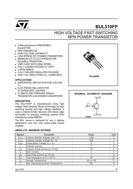
® BUL310FP HIGH VOLTAGE FAST-SWITCHING NPN POWER TRANSISTOR ■ ■ ■ ■ ■ ■ ■ ■ ■ ■ STMicroelectronics PREFERRED SALESTYPE NPN TRANSISTOR HIGH VOLTAGE CAPABILITY LOW SPREAD OF DYNAMIC PARAMETERS MINIMUM LOT-TO-LOT SPREAD FOR RELIABLE OPERATION VERY HIGH SWITCHING SPEED FULLY CHARACTERIZED AT 125 o C LARGE RBSOA FULLY MOLDED INSULATED PACKAGE 2000 V DC INSULATION (U.L. COMPLIANT) APPLICATIONS ■ HORIZONTAL DEFLECTION FOR COLOUR TV ■ ELECTRONIC BALLASTS FOR FLUORESCENT LIGHTING ■ FLYBACK AND FORWARD SINGLE TRANSISTOR LOW POWER CONVERTERS TO-220FP 1 2 3 INTERNAL SCHEMATIC DIAGRAM DESCRIPTION The BUL310FP is manufactured using high voltage Multi Epitaxial Planar technology for high switching speeds and high voltage capability. It uses a Cellular Emitter structure with planar edge termination to enhance switching speeds while maintaining a wide RBSOA. The BUL series is designed for use in lighting applications and low cost switch-mode power supplies. ABSOLUTE MAXIMUM RATINGS Symbol Parameter Value Unit VCES Collector-Emitter Voltage (VBE = 0) 1000 V V CEO Collector-Emitter Voltage (I B = 0) 500 V V EBO Emitter-Base Voltage (I C = 0) 9 V I C Collector Current 5 A ICM Collector Peak Current (tp
- Page 2 and 3: BUL310FP THERMAL DATA R thj-case Rt
- Page 4 and 5: BUL310FP Reverse Biased SOA Figure
- Page 6: BUL310FP Information furnished is b
®<br />
BUL310FP<br />
HIGH VOLTAGE FAST-SWITCHING<br />
NPN POWER TRANSISTOR<br />
■<br />
■<br />
■<br />
■<br />
■<br />
■<br />
■<br />
■<br />
■<br />
■<br />
STMicroelectronics PREFERRED<br />
SALESTYPE<br />
NPN TRANSISTOR<br />
HIGH VOLTAGE CAPABILITY<br />
LOW SPREAD OF DYNAMIC PARAMETERS<br />
MINIMUM LOT-TO-LOT SPREAD FOR<br />
RELIABLE OPERATION<br />
VERY HIGH SWITCHING SPEED<br />
FULLY CHARACTERIZED AT 125 o C<br />
LARGE RBSOA<br />
FULLY MOLDED INSULATED PACKAGE<br />
2000 V DC INSULATION (U.L. COMPLIANT)<br />
APPLICATIONS<br />
■ HORIZONTAL DEFLECTION FOR COLOUR<br />
TV<br />
■ ELECTRONIC BALLASTS FOR<br />
FLUORESCENT LIGHTING<br />
■ FLYBACK AND FORWARD SINGLE<br />
TRANSISTOR LOW POWER CONVERTERS<br />
TO-220FP<br />
1 2 3<br />
INTERNAL SCHEMATIC DIAGRAM<br />
DESCRIPTION<br />
The BUL310FP is manufactured using <strong>high</strong><br />
<strong>voltage</strong> Multi Epitaxial Planar technology for <strong>high</strong><br />
<strong>switching</strong> speeds and <strong>high</strong> <strong>voltage</strong> capability. It<br />
uses a Cellular Emitter structure with planar edge<br />
termination to enhance <strong>switching</strong> speeds while<br />
maintaining a wide RBSOA.<br />
The BUL series is designed for use in lighting<br />
applications and low cost switch-mode <strong>power</strong><br />
supplies.<br />
ABSOLUTE MAXIMUM RATINGS<br />
Symbol Parameter Value Unit<br />
VCES Collector-Emitter Voltage (VBE = 0) 1000 V<br />
V CEO Collector-Emitter Voltage (I B = 0) 500 V<br />
V EBO Emitter-Base Voltage (I C = 0) 9 V<br />
I C Collector Current 5 A<br />
ICM Collector Peak Current (tp
BUL310FP<br />
THERMAL DATA<br />
R thj-case<br />
Rthj-amb<br />
Thermal Resistance Junction-Case<br />
Thermal Resistance Junction-Ambient<br />
Max<br />
Max<br />
3.5<br />
62.5<br />
o C/W<br />
o C/W<br />
ELECTRICAL CHARACTERISTICS (T case = 25 o C unless otherwise specified)<br />
Symbol Parameter Test Conditions Min. Typ. Max. Unit<br />
ICES<br />
ICEO<br />
VCEO(sus)∗<br />
VEBO<br />
V CE(sat)∗<br />
V BE(sat)∗<br />
Collector Cut-off<br />
Current (V BE = 0)<br />
Collector Cut-off<br />
Current (I B = 0)<br />
Collector-Emitter<br />
Sustaining Voltage<br />
(IB = 0)<br />
Emitter-Base Voltage<br />
(I C = 0)<br />
Collector-Emitter<br />
Saturation Voltage<br />
Base-Emitter<br />
Saturation Voltage<br />
VCE = 1000 V<br />
V CE = 1000 V<br />
T j = 125 o C<br />
100<br />
500<br />
VCE = 500 V 250 µA<br />
IC = 100 mA L= 25 mH 500 V<br />
IE = 10 mA 9 V<br />
I C = 1 A<br />
I C = 2 A<br />
IC = 3 A<br />
I C = 1 A<br />
I C = 2 A<br />
I C = 3 A<br />
I B = 0.2 A<br />
I B = 0.4 A<br />
IB = 0.6 A<br />
I B = 0.2 A<br />
I B = 0.4 A<br />
I B = 0.6 A<br />
h FE∗ DC Current Gain I C = 10 mA V CE = 5 V<br />
IC = 3 A VCE = 2.5 V<br />
t s<br />
t f<br />
INDUCTIVE LOAD<br />
Storage Time<br />
Fall Time<br />
I C = 2 A I B1 = 0.4 A<br />
V BE(off) = -5 V R BB = 0 Ω<br />
VCL = 250 V L = 200 µH<br />
(see figure 1)<br />
INDUCTIVE LOAD I C = 2 A I B1 = 0.4 A<br />
t s Storage Time<br />
V BE(off) = -5V R BB = 0 Ω<br />
t f Fall Time<br />
V CL = 250 V L = 200 µH<br />
T j = 125 o C (see figure 1)<br />
∗ Pulsed: Pulse duration = 300 µs, duty cycle 1.5 %<br />
0.5<br />
0.7<br />
1.1<br />
1<br />
1.1<br />
1.2<br />
10<br />
6 10 14<br />
1.2<br />
80<br />
1.8<br />
150<br />
1.9<br />
160<br />
µA<br />
µA<br />
V<br />
V<br />
V<br />
V<br />
V<br />
V<br />
µs<br />
ns<br />
µs<br />
ns<br />
Safe Operating Areas<br />
Derating Curve<br />
2/6
BUL310FP<br />
DC Current Gain<br />
DC Current Gain<br />
Collector Emitter Saturation Voltage<br />
Base Emitter Saturation Voltage<br />
Inductive Load Fall Time<br />
Inductive Load Storage Time<br />
3/6
BUL310FP<br />
Reverse Biased SOA<br />
Figure 1: Inductive Load Switching Test Circuit<br />
(1) Fast electronic switch<br />
(2) Non-inductive Resistor<br />
(3) Fast recovery rectifier<br />
4/6
BUL310FP<br />
TO-220FP MECHANICAL DATA<br />
DIM.<br />
mm<br />
inch<br />
MIN. TYP. MAX. MIN. TYP. MAX.<br />
A 4.4 4.6 0.173 0.181<br />
B 2.5 2.7 0.098 0.106<br />
D 2.5 2.75 0.098 0.108<br />
E 0.45 0.7 0.017 0.027<br />
F 0.75 1 0.030 0.039<br />
F1 1.15 1.7 0.045 0.067<br />
F2 1.15 1.7 0.045 0.067<br />
G 4.95 5.2 0.195 0.204<br />
G1 2.4 2.7 0.094 0.106<br />
H 10 10.4 0.393 0.409<br />
L2 16 0.630<br />
L3 28.6 30.6 1.126 1.204<br />
L4 9.8 10.6 0.385 0.417<br />
L6 15.9 16.4 0.626 0.645<br />
L7 9 9.3 0.354 0.366<br />
Ø 3 3.2 0.118 0.126<br />
E<br />
D<br />
A<br />
B<br />
L6<br />
L7<br />
L3<br />
¯<br />
F1<br />
F<br />
G1<br />
H<br />
G<br />
L2<br />
F2<br />
L4<br />
1 2 3<br />
5/6
BUL310FP<br />
Information furnished is believed to be accurate and reliable. However, STMicroelectronics assumes no responsibility for the consequences<br />
of use of such information nor for any infringement of patents or other rights of third parties which may result from its use. No license is<br />
granted by implication or otherwise under any patent or patent rights of STMicroelectronics. Specification mentioned in this publication are<br />
subject to change without notice. This publication supersedes and replaces all information previously supplied. STMicroelectronics products<br />
are not authorized for use as critical components in life support devices or systems without express written approval of STMicroelectronics.<br />
The ST logo is a trademark of STMicroelectronics<br />
© 2003 STMicroelectronics – Printed in Italy – All Rights Reserved<br />
STMicroelectronics GROUP OF COMPANIES<br />
Australia - Brazil - Canada - China - Finland - France - Germany - Hong Kong - India - Israel - Italy - Japan - Malaysia - Malta - Morocco -<br />
Singapore - Spain - Sweden - Switzerland - United Kingdom - United States.<br />
http://www.st.com<br />
6/6


