T260XW02 VA Customer Part No/Project Name - M-COMP
T260XW02 VA Customer Part No/Project Name - M-COMP
T260XW02 VA Customer Part No/Project Name - M-COMP

Create successful ePaper yourself
Turn your PDF publications into a flip-book with our unique Google optimized e-Paper software.
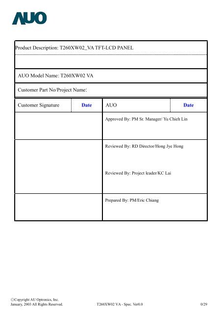
Product Description: <strong>T260XW02</strong>_<strong>VA</strong> TFT-LCD PANEL<br />
AUO Model <strong>Name</strong>: <strong>T260XW02</strong> <strong>VA</strong><br />
<strong>Customer</strong> <strong>Part</strong> <strong>No</strong>/<strong>Project</strong> <strong>Name</strong>:<br />
<strong>Customer</strong> Signature Date AUO Date<br />
Approved By: PM Sr. Manager/ Yu Chieh Lin<br />
Reviewed By: RD Director/Hong Jye Hong<br />
Reviewed By: <strong>Project</strong> leader/KC Lai<br />
Prepared By: PM/Eric Chiang<br />
◎Copyright AU Optronics, Inc.<br />
January, 2003 All Rights Reserved. <strong>T260XW02</strong> <strong>VA</strong> - Spec. Ver0.0 0/29<br />
<strong>No</strong> Reproduction and Redistribution Allowed
Document Version: 0.0<br />
Date: 2007/1/26<br />
Product Specifications<br />
26.0” WXGA Color TFT-LCD Module<br />
Model <strong>Name</strong>: <strong>T260XW02</strong> <strong>VA</strong><br />
(*) Preliminary Specifications<br />
() Final Specifications<br />
◎Copyright AU Optronics, Inc.<br />
January, 2003 All Rights Reserved. <strong>T260XW02</strong> <strong>VA</strong> - Spec. Ver0.0 1/29<br />
<strong>No</strong> Reproduction and Redistribution Allowed
<strong>No</strong><br />
Contents<br />
ITEM<br />
COVER<br />
CONTENTS<br />
RECORD OF REVISIONS<br />
1 GENERAL DESCRIPTION<br />
2 ABSOLUTION MAXIMUM RATINGS<br />
3 ELECTRICAL SPECIFICATIONS<br />
3-1 ELECTRICAL CHARACTERISTICS<br />
3-2 INTERFACE CONNECTIONS<br />
3-3 SIGNAL TIMING SPECIFICATIONS<br />
3-4 SIGNAL TIMING WAVEFORMS<br />
3-5 COLOR INPUT DATA REFERENCE<br />
3-6 POWER SEQUENCE for LCD<br />
3-7 POWER SEQUENCE for INVERTER<br />
4 OPTICAL SPECIFICATIONS<br />
5 MECHANICAL CHARACTERISTICS<br />
5-1 Front view<br />
5-2 Rear view<br />
6 RELIABILITY<br />
7 INTERNATIONAL STANDARDS<br />
7-1 SAFETY<br />
7-2 EMC<br />
7-3 Green<br />
8 PACKING<br />
9 PRECAUTIONS<br />
◎Copyright AU Optronics, Inc.<br />
January, 2003 All Rights Reserved. <strong>T260XW02</strong> <strong>VA</strong> - Spec. Ver0.0 2/29<br />
<strong>No</strong> Reproduction and Redistribution Allowed
Record of Revision<br />
Version Date <strong>No</strong> Old Description New Description Remark<br />
0.0 2007/01/26 First Release<br />
◎Copyright AU Optronics, Inc.<br />
January, 2003 All Rights Reserved. <strong>T260XW02</strong> <strong>VA</strong> - Spec. Ver0.0 3/29<br />
<strong>No</strong> Reproduction and Redistribution Allowed
1. General Description<br />
This specification applies to the 26.0 inch Color TFT-LCD Module <strong>T260XW02</strong>. This LCD module has a TFT<br />
active matrix type liquid crystal panel 1366x768 pixels, and diagonal size of 26.0 inch. This module supports<br />
1366x768 XGA-WIDE mode (<strong>No</strong>n-interlace).<br />
Each pixel is divided into Red, Green and Blue sub-pixels or dots which are arranged in vertical stripes. Gray<br />
scale or the brightness of the sub-pixel color is determined with a 8-bit gray scale signal for each dot.<br />
The <strong>T260XW02</strong> has been designed to apply the 8-bit 1 channel LVDS interface method. It is intended to<br />
support displays where high brightness, wide viewing angle, high color saturation, and high color depth are<br />
very important.<br />
* General Information<br />
Items Specification Unit <strong>No</strong>te<br />
Active Screen Size 26.0 inches<br />
Display Area 575.769 (H) x 323.712(V) mm<br />
Pixel Pitch 0.4215 mm<br />
Outline Dimension 626.0 (H) x 373.0 (V) x 47.5(D) mm With inverter<br />
Driver Element<br />
a-Si TFT active matrix<br />
Display Colors 16.7M Colors<br />
Number of Pixels 1366 x 768 Pixel<br />
Pixel Arrangement<br />
RGB vertical stripe<br />
Display Mode<br />
<strong>No</strong>rmally Black<br />
BL Structure<br />
6 U-Lamps<br />
Surface Treatment<br />
AG, 3H<br />
Green<br />
RoHS compliance<br />
◎Copyright AU Optronics, Inc.<br />
January, 2003 All Rights Reserved. <strong>T260XW02</strong> <strong>VA</strong> - Spec. Ver0.0 4/29<br />
<strong>No</strong> Reproduction and Redistribution Allowed
2. Absolute Maximum Ratings<br />
The following are maximum values which, if exceeded, may cause faulty operation or damage to the unit.<br />
Item Symbol Min Max Unit Conditions<br />
Logic/LCD Drive Voltage V CC -0.3 6.0 [Volt] <strong>No</strong>te 1<br />
LVDS Option Control Voltage V LVDSOPT -0.3 3.6 [Volt] <strong>No</strong>te 1<br />
BLU Input Voltage VDDB -0.3 27.0 [Volt] <strong>No</strong>te 1<br />
External Analog Dimming Control Voltage VDIM -0.3 6.0 [Volt] <strong>No</strong>te 1<br />
On/Off Control Voltage VBLON -0.3 6.0 [Volt] <strong>No</strong>te 1<br />
External PWM Dimming Control Voltage EV PWM -0.3 6.0 [Volt] <strong>No</strong>te 1<br />
Operating Temperature TOP 0 +50 [ o C] <strong>No</strong>te 2<br />
Operating Humidity HOP 10 90 [%RH] <strong>No</strong>te 2<br />
Storage Temperature TST -20 +60 [ o C] <strong>No</strong>te 2<br />
Storage Humidity HST 10 90 [%RH] <strong>No</strong>te 2<br />
<strong>No</strong>te 1: Duration = 1 sec<br />
<strong>No</strong>te 2: Maximum Wet-Bulb should be 39℃ and <strong>No</strong> condensation.<br />
◎Copyright AU Optronics, Inc.<br />
January, 2003 All Rights Reserved. <strong>T260XW02</strong> <strong>VA</strong> - Spec. Ver0.0 5/29<br />
<strong>No</strong> Reproduction and Redistribution Allowed
3. Electrical Specification<br />
The <strong>T260XW02</strong> requires two power inputs. One is employed to power the LCD electronics and to drive the<br />
TFT array and liquid crystal. The second input power for the BLU is to power inverter.<br />
3-1 Electrical Characteristics<br />
Values<br />
Parameter<br />
Symbol<br />
Min. Typ. Max.<br />
Unit <strong>No</strong>tes<br />
LCD:<br />
Power Supply Input Voltage V cc 4.5 5.0 5.5 V<br />
Power Supply Input Current Icc - 1.40 1.78 A 1<br />
Power Consumption Pc - 7.0 9.0 Watt 1<br />
Inrush Current I RUSH - - 3.0 A 2<br />
LVDS Interface:<br />
Differential Input High Threshold<br />
Voltage<br />
VTH +100 mV<br />
Differential Input Low Threshold<br />
Voltage<br />
VTL -100 mV<br />
Common Input Voltage VCIM 1.10 1.25 1.40 V<br />
CMOS Interface:<br />
Input High Threshold Voltage VIH(High) 2.4 3.3 Vdc<br />
Input Low Threshold Voltage VIL(Low) 0 0.7 Vdc<br />
Backlight Power Consumption - - 85.4 Watt 3<br />
Life Time 50,000 60,000 Hours 4<br />
<strong>No</strong>te :<br />
1. Vcc=5.0V, Fv=60Hz, Fclk= 85.0 MHz , 25℃. , Test Pattern : White Pattern<br />
2. Vcc rising time = 470 µ s , Vcc=5.0V<br />
3. VDDB=24V, VDIM=3.3V, EDPWM=100%, test in the whole period from VDDB power on to power off.<br />
4. The performance of the Lamp in LCM, for example: lifetime or brightness, is extremely influenced by the characteristics<br />
of the DC-AC Inverter. So all the parameters of an inverter should be carefully designed so as not to produce too much<br />
leakage current from high-voltage output of the inverter. When you design or order the inverter, please make sure<br />
unwanted lighting caused by the mismatch of the lamp and the inverter (no lighting, flicker, etc) never occurs. When you<br />
confirm it, the LCD Assembly should be operated in the same condition as installed in your instrument.<br />
5. Do not attach a conducting tape to lamp connecting wire. If the lamp wire attach to conducting tape, TFT-LCD Module<br />
have a low luminance and the inverter has abnormal action because leakage current occurs between lamp wire and<br />
conducting tape.<br />
6. The relative humidity must not exceed 80% non-condensing at temperatures of 40℃ or less. At temperatures greater than<br />
40℃, the wet bulb temperature must not exceed 39℃. When operate at low temperatures, the brightness of CCFL will<br />
drop and the lifetime of CCFL will be reduced.<br />
◎Copyright AU Optronics, Inc.<br />
January, 2003 All Rights Reserved. <strong>T260XW02</strong> <strong>VA</strong> - Spec. Ver0.0 6/29<br />
<strong>No</strong> Reproduction and Redistribution Allowed
3-2 Interface Connections<br />
- LCD connector (CN1): JAE FI-E30S<br />
- LVDS Transmitter: SN75LVDS83(Texas Instruments) or equivalent<br />
<strong>No</strong>te:<br />
1. All GND (ground) pins should be connected together and should also be connected to the LCD’s metal frame. All Vcc<br />
(power input) pins should be connected together.<br />
Pin <strong>No</strong> Symbol Description Default<br />
1 N.C. <strong>No</strong> Connection ( Auo internal Test Pin)<br />
2 N.C. <strong>No</strong> Connection ( Auo internal Test Pin)<br />
3 N.C. <strong>No</strong> Connection ( Auo internal Test Pin)<br />
4 GND Power Ground<br />
5 Rx0- Negative LVDS differential data input<br />
6 Rx0+ Positive LVDS differential data input<br />
7 GND Power Ground<br />
8 Rx1- Negative LVDS differential data input<br />
9 Rx1+ Positive LVDS differential data input<br />
10 GND Power Ground<br />
11 Rx2- Negative LVDS differential data input<br />
12 Rx2+ Positive LVDS differential data input<br />
13 GND Power Ground<br />
14 RxCLK- Negative LVDS differential clock input<br />
15 RxCLK+ Positive LVDS differential clock input<br />
16 GND Power Ground<br />
17 Rx3- Negative LVDS differential data input<br />
18 Rx3+ Positive LVDS differential data input<br />
19 GND Power Ground<br />
20 N.C. <strong>No</strong> Connection ( Auo internal Test Pin)<br />
21 LVDS Option Pull Low : JETDA LVDS format; Pull High or N.C.: NS LVDS format<br />
22 N.C. <strong>No</strong> Connection ( Auo internal Test Pin)<br />
23 GND Power Ground<br />
24 GND Power Ground<br />
25 GND Power Ground<br />
26 V CC +5V Power Input<br />
27 V CC +5V Power Input<br />
28 V CC +5V Power Input<br />
29 V CC +5V Power Input<br />
30 V CC +5V Power Input<br />
** LVDS Option: H (3.3V) or N.C.Ł NS<br />
L (GND) Ł JETDA<br />
◎Copyright AU Optronics, Inc.<br />
January, 2003 All Rights Reserved. <strong>T260XW02</strong> <strong>VA</strong> - Spec. Ver0.0 7/29<br />
<strong>No</strong> Reproduction and Redistribution Allowed
LVDS Option = L (GND)Ł JETDA Format<br />
Previous Cycle Current Cycle Next Cycle<br />
Clock<br />
RIN0+<br />
RIN0-<br />
R3<br />
R2<br />
G2<br />
R7<br />
R6<br />
R5<br />
R4<br />
R3<br />
R2<br />
G2<br />
RIN1+<br />
RIN1-<br />
G4<br />
G3<br />
B3<br />
B2<br />
G7<br />
G6<br />
G5<br />
G4<br />
G3<br />
B3<br />
RIN2+<br />
RIN2-<br />
B5<br />
B4<br />
DE<br />
NA<br />
NA<br />
B7<br />
B6<br />
B5<br />
B4<br />
DE<br />
RIN3+<br />
RIN3-<br />
R1<br />
R0<br />
NA<br />
B1<br />
B0<br />
G1<br />
G0<br />
R1<br />
R0<br />
NA<br />
LVDS Option = H (3.3V) or N.C.Ł NS Format<br />
Previous Cycle Current Cycle Next Cycle<br />
Clock<br />
RIN0+<br />
RIN0-<br />
R1<br />
R0<br />
G0<br />
R5<br />
R4<br />
R3<br />
R2<br />
R1<br />
R0<br />
G0<br />
RIN1+<br />
RIN1-<br />
G2<br />
G1<br />
B1<br />
B0<br />
G5<br />
G4<br />
G3<br />
G2<br />
G1<br />
B1<br />
RIN2+<br />
RIN2-<br />
B3<br />
B2<br />
DE<br />
NA<br />
NA<br />
B5<br />
B4<br />
B3<br />
B2<br />
DE<br />
RIN3+<br />
RIN3-<br />
R7<br />
R6<br />
NA<br />
B7<br />
B6<br />
G7<br />
G6<br />
R7<br />
R6<br />
NA<br />
◎Copyright AU Optronics, Inc.<br />
January, 2003 All Rights Reserved. <strong>T260XW02</strong> <strong>VA</strong> - Spec. Ver0.0 8/29<br />
<strong>No</strong> Reproduction and Redistribution Allowed
BACKLIGHT CONNECTOR PIN CONFIGURATION<br />
1. Electrical specification<br />
(Ta=25±5℃)<br />
<strong>No</strong> ITEM SYMBOL CONDITION MIN TYP MAX UNIT <strong>No</strong>te<br />
1 Input Voltage V DDB --- 21.6 24.0 26.4 V<br />
2 Input Current (Turn on Condition) I DDB<br />
V DDB =24V<br />
VDIM=3.3V 3.23 3.39 3.55 A 1<br />
3 Input Power (Turn on Condition) P DDB<br />
4 Input Current (Stable Condition) I DDB<br />
5 Input Power (Stable Condition) P DDB<br />
6 Input inrush current, 20ms I RUSH<br />
V DDB =24V<br />
VDIM=3.3V --- 81.4 85.4 W 1<br />
V DDB =24V<br />
VDIM=3.3V 2.93 3.08 3.23 A 1<br />
V DDB =24V<br />
VDIM=3.3V 70.3 74 77.7 W 1<br />
V DD =24V<br />
VDIM=3.3V --- --- 6 A<br />
7 Output Frequency F BL V DD =24V 56 58 60 kHz<br />
ON V DD =24V 2.0 3.3 5.0 V<br />
8 ON/OFF Control Voltage V BLON<br />
OFF V DD =24V 0.0 --- 0.8 V or Open<br />
9 ON/OFF Control Current I BLON V DD =24V -1 --- 1.5 mA<br />
MAX V DD =24V --- 3.3 --- V or Open<br />
10 Dimming Control Voltage V DIM<br />
MIN V DD =24V --- 0.0 --- V<br />
11 Dimming Control Current I DIM MIN V DD =24V --- --- 1.5 mA<br />
◎Copyright AU Optronics, Inc.<br />
January, 2003 All Rights Reserved. <strong>T260XW02</strong> <strong>VA</strong> - Spec. Ver0.0 9/29<br />
<strong>No</strong> Reproduction and Redistribution Allowed
2. Input specification<br />
Pin <strong>No</strong> Symbol Description Default<br />
1 VDDB Operating Voltage Supply, +24V DC regulated 24V<br />
2 VDDB Operating Voltage Supply, +24V DC regulated 24V<br />
3 VDDB Operating Voltage Supply, +24V DC regulated 24V<br />
4 VDDB Operating Voltage Supply, +24V DC regulated 24V<br />
5 VDDB Operating Voltage Supply, +24V DC regulated 24V<br />
6 GND Ground GND<br />
7 GND Ground GND<br />
8 GND Ground GND<br />
9 GND Ground GND<br />
10 GND Ground GND<br />
11 DET<br />
Inverter OK: High (min/typ/max: 3/3.3/3.6)<br />
Inverter NG: Low/GND ( min/typ/max:-0.3/0/0.8)<br />
-<br />
Inverter side open collector 10 mA<br />
12 VBLON<br />
BL on/off: High (3.3V) for BL ON<br />
Open/Low (GND) for BL OFF<br />
-<br />
Output impedance: 4.7KΩ<br />
13 VDIM<br />
Analog brightness control<br />
Brightness max (min/typ/max: 3/3.3/3.6)<br />
Brightness min(min/typ/max: -0.3/0/0.36)<br />
-<br />
Output impedance: 1KΩ<br />
14 NC NC -<br />
CN1: S14B-PHA-SM (JST) or equivalent<br />
CN2~7: BDAMR-02<strong>VA</strong>S-1 (JST) or equivalent<br />
◎Copyright AU Optronics, Inc.<br />
January, 2003 All Rights Reserved. <strong>T260XW02</strong> <strong>VA</strong> - Spec. Ver0.0 10/29<br />
<strong>No</strong> Reproduction and Redistribution Allowed
3. Backlight Diagram<br />
◎Copyright AU Optronics, Inc.<br />
January, 2003 All Rights Reserved. <strong>T260XW02</strong> <strong>VA</strong> - Spec. Ver0.0 11/29<br />
<strong>No</strong> Reproduction and Redistribution Allowed
3-3 Signal Timing Specifications<br />
This is the signal timing required at the input of the User connector. All of the interface signal timing should<br />
be satisfied with the following specifications for its proper operation.<br />
* Timing Table<br />
DE only Mode<br />
Vertical Frequency<br />
Signal Item Symbol Min. Typ. Max. Unit<br />
Period Tv 789 806 1000 Th<br />
Vertical<br />
Section<br />
Active Tdisp(v) 768 Th<br />
Horizontal<br />
Section<br />
Blanking Tblk (v) 21 38 232 Th<br />
Period Th 1414 1560 1722 Tclk<br />
Active Tdisp(h) 1366 Tclk<br />
Blanking Tblk (h) 48 194 356 Tclk<br />
LVDS Clock Frequency Fclk (1/Tclk) 65 76 88 MHz<br />
Vertical<br />
Frequency<br />
Horizontal<br />
Frequency<br />
Frequency Fv 47 60 63 Hz<br />
Frequency Fh 43 48 53 kHz<br />
*1) Display position is specific by the rise of DE signal only.<br />
Horizontal display position is specified by the falling edge of 1 st Clock right after the rise of DE, is displayed<br />
on the left edge of the screen.<br />
Vertical display position is specified by the rise of DE after a “Low” level period equivalent to eight times of<br />
horizontal period. The 1 st data corresponding to one horizontal line after the rise of DE is displayed at the top<br />
line of screen.<br />
*2) If a period of DE “High” is less than 1366 Clock or less than 768 lines, the rest of the screen displays<br />
black.<br />
*3) The display position does not fit to the screen if a period of DE “High” and the effective data period do<br />
not synchronize with each other.<br />
◎Copyright AU Optronics, Inc.<br />
January, 2003 All Rights Reserved. <strong>T260XW02</strong> <strong>VA</strong> - Spec. Ver0.0 12/29<br />
<strong>No</strong> Reproduction and Redistribution Allowed
3-4 Signal Timing Waveforms<br />
DE<br />
RGB<br />
Data<br />
CLK<br />
DE<br />
RGB Data<br />
768<br />
Line<br />
Tv<br />
Tdisp(v)<br />
Th<br />
Invalid Data 1<br />
2<br />
3<br />
4<br />
768<br />
Invalid Data<br />
Line Line Line Line<br />
Line<br />
Tclk<br />
Th<br />
Tdisp(h)<br />
Pixel<br />
1366<br />
Invalid Data<br />
Pixel<br />
1<br />
Pixel<br />
2<br />
Pixel<br />
3<br />
Pixel<br />
4<br />
Pixel<br />
5<br />
Pixel<br />
6<br />
Pixel<br />
1366<br />
Invalid Data<br />
Pixel<br />
1<br />
Pixel<br />
2<br />
◎Copyright AU Optronics, Inc.<br />
January, 2003 All Rights Reserved. <strong>T260XW02</strong> <strong>VA</strong> - Spec. Ver0.0 13/29<br />
<strong>No</strong> Reproduction and Redistribution Allowed
3-5 Color Input Data Reference<br />
The brightness of each primary color (red, green and blue) is based on the 8 bit gray scale data input for the<br />
color; the higher the binary input, the brighter the color. The table below provides a reference for color versus<br />
data input.<br />
COLOR DATA REFERENCE<br />
Input Color Data<br />
Color<br />
RED<br />
GREEN<br />
BLUE<br />
MSB<br />
LSB MSB<br />
LSB MSB<br />
LSB<br />
R7 R6 R5 R4 R3 R2 R1 R0 G7 G6 G5 G4 G3 G2 G1 G0 B7 B6 B5 B4 B3 B2 B1 B0<br />
Black 0 0 0 0 0 0 0 0 0 0 0 0 0 0 0 0 0 0 0 0 0 0 0 0<br />
Red(255) 1 1 1 1 1 1 1 1 0 0 0 0 0 0 0 0 0 0 0 0 0 0 0 0<br />
Green(255) 0 0 0 0 0 0 0 0 1 1 1 1 1 1 1 1 0 0 0 0 0 0 0 0<br />
Basic Blue(255) 0 0 0 0 0 0 0 0 0 0 0 0 0 0 0 0 1 1 1 1 1 1 1 1<br />
Color Cyan 0 0 0 0 0 0 0 0 1 1 1 1 1 1 1 1 1 1 1 1 1 1 1 1<br />
Magenta 1 1 1 1 1 1 1 1 0 0 0 0 0 0 0 0 1 1 1 1 1 1 1 1<br />
Yellow 1 1 1 1 1 1 1 1 1 1 1 1 1 1 1 1 0 0 0 0 0 0 0 0<br />
White 1 1 1 1 1 1 1 1 1 1 1 1 1 1 1 1 1 1 1 1 1 1 1 1<br />
RED(000) 0 0 0 0 0 0 0 0 0 0 0 0 0 0 0 0 0 0 0 0 0 0 0 0<br />
RED(001) 0 0 0 0 0 0 0 1 0 0 0 0 0 0 0 0 0 0 0 0 0 0 0 0<br />
RED ----<br />
RED(254) 1 1 1 1 1 1 1 0 0 0 0 0 0 0 0 0 0 0 0 0 0 0 0 0<br />
RED(255) 1 1 1 1 1 1 1 1 0 0 0 0 0 0 0 0 0 0 0 0 0 0 0 0<br />
GREEN(000) 0 0 0 0 0 0 0 0 0 0 0 0 0 0 0 0 0 0 0 0 0 0 0 0<br />
GREEN(001) 0 0 0 0 0 0 0 0 0 0 0 0 0 0 0 1 0 0 0 0 0 0 0 0<br />
GREEN ----<br />
GREEN(254) 0 0 0 0 0 0 0 0 1 1 1 1 1 1 1 0 0 0 0 0 0 0 0 0<br />
GREEN(255) 0 0 0 0 0 0 0 0 1 1 1 1 1 1 1 1 0 0 0 0 0 0 0 0<br />
BLUE(000) 0 0 0 0 0 0 0 0 0 0 0 0 0 0 0 0 0 0 0 0 0 0 0 0<br />
BLUE(001) 0 0 0 0 0 0 0 0 0 0 0 0 0 0 0 0 0 0 0 0 0 0 0 1<br />
BLUE -------<br />
BLUE(254) 0 0 0 0 0 0 0 0 0 0 0 0 0 0 0 0 1 1 1 1 1 1 1 0<br />
BLUE(255) 0 0 0 0 0 0 0 0 0 0 0 0 0 0 0 0 1 1 1 1 1 1 1 1<br />
◎Copyright AU Optronics, Inc.<br />
January, 2003 All Rights Reserved. <strong>T260XW02</strong> <strong>VA</strong> - Spec. Ver0.0 14/29<br />
<strong>No</strong> Reproduction and Redistribution Allowed
3-6 Power Sequence for LCD<br />
Parameter<br />
Values<br />
Min. Typ. Max.<br />
Units<br />
t1 1 - 30 ms<br />
t2 10 - 100 ms<br />
t3 550*1 - - ms<br />
t4 100 - - ms<br />
t5 50 - - ms<br />
t6 -- - 300 ms<br />
t7 300 - - ms<br />
*1: If t3=200ms, input black signal till 550ms from system is necessary.<br />
In case of t3
3-7 Power Sequence for Inverter<br />
Parameter<br />
Values<br />
Min. Typ. Max.<br />
Units<br />
T1 20 - - ms<br />
T2 10 - - ms<br />
T3 0 - - ms<br />
T4 50 - - ms<br />
T5 0 - - ms<br />
◎Copyright AU Optronics, Inc.<br />
January, 2003 All Rights Reserved. <strong>T260XW02</strong> <strong>VA</strong> - Spec. Ver0.0 16/29<br />
<strong>No</strong> Reproduction and Redistribution Allowed
4. Optical Specification<br />
Optical characteristics are determined after the unit has been ‘ON’ and stable for approximately 45 minutes in<br />
a dark environment at 25 ℃ . The values specified are at an approximate distance 50cm from the LCD surface<br />
at a viewing angle of Φ and θequal to 0°. Signal generator used for measurement is “Chroma 2913” and<br />
signal setting follows the typical value shown in page 13 with vertical frequency range A (fv=60Hz).<br />
Meanwhile, dimmer is 3.3(V) for its maximum setting.<br />
Fig.1 1 presents additional information concerning the measurement equipment and method.<br />
Values<br />
Parameter<br />
Symbol<br />
Units <strong>No</strong>tes<br />
Min. Typ. Max.<br />
Contrast Ratio CR (1200) (1500) 1<br />
Surface Luminance, white LWH (400) (500) cd/m2 2<br />
Luminance Variation δ WHITE 9 p 1.3 3<br />
Response Rise Time Tr R 15<br />
Time Decay Time Tr D 5<br />
ms 4<br />
Gray to Gray Tγ 8 ms 5<br />
Color Gamut NTSC 72 %<br />
Color Coordinates<br />
RED<br />
R X 0.640<br />
R Y 0.330<br />
G X 0.290<br />
GREEN<br />
G Y 0.600<br />
Typ.-0.03<br />
B X 0.150<br />
BLUE<br />
0.060<br />
B Y<br />
Typ.+0.03<br />
WHITE<br />
W X 0.280<br />
W Y<br />
0.290<br />
Viewing Angle<br />
x axis, right(φ=0°) θ r 88 Degree<br />
x axis, left(φ=180°) θ l 88 Degree 6<br />
y axis, up(φ=90°) θ u 88 Degree<br />
y axis, down (φ=0°) θ d 88 Degree<br />
◎Copyright AU Optronics, Inc.<br />
January, 2003 All Rights Reserved. <strong>T260XW02</strong> <strong>VA</strong> - Spec. Ver0.0 17/29<br />
<strong>No</strong> Reproduction and Redistribution Allowed
<strong>No</strong>te:<br />
1. Contrast Ratio (CR) is defined mathematically as:<br />
Contrast Ratio=<br />
Surface Luminance of L on1<br />
Surface Luminance of L off1<br />
2. Surface luminance is luminance value at point 1 across the LCD surface 50cm from the surface with all pixels displaying white.<br />
From more information see FIG 2. When V DDB = 24V, I DDB = 3.5A. L WH =Lon1<br />
Where Lon1 is the luminance with all pixels displaying white at center 1 location.<br />
3. The variation in surface luminance, δ WHITE is defined (center of Screen) as:<br />
δ WHITE(9P) = Maximum(L on1 , L on2 ,…L on9 ) / Minimum(L on1 , L on2 ,…,L on9 )<br />
4. Response time is the time required for the display to transition from black to white(Rise Time, Tr R ) and from white to black<br />
(Decay Time, Tr D ). For additional information see FIG3.<br />
5. Tγ is the response time between any two gray scale (steps size=32 levels) and is based on f v =60Hz to optimize.<br />
6. Viewing angle is the angle at which the contrast ratio is greater than 10. The angles are determined for the horizontal or x axis<br />
and the vertical or y axis with respect to the z axis which is normal to the LCD surface. For more information see FIG4.<br />
FIG. 2 Luminance<br />
V<br />
H/2<br />
1 2 3<br />
4 5 6<br />
H<br />
H/6<br />
7 8<br />
V/6<br />
V/2<br />
◎Copyright AU Optronics, Inc.<br />
January, 2003 All Rights Reserved. <strong>T260XW02</strong> <strong>VA</strong> - Spec. Ver0.0 18/29<br />
<strong>No</strong> Reproduction and Redistribution Allowed
FIG.3 Response Time<br />
The response time is defined as the following figure and shall be measured by switching the input signal for<br />
“black” and “white”.<br />
Any brighter gray level (White)<br />
Any brighter gray level (White)<br />
100%<br />
90%<br />
Optical<br />
Response<br />
a n c e<br />
10%<br />
0<br />
Tr D<br />
Any darker gray (Black)<br />
Tr R<br />
Time<br />
FIG.4 Viewing angle<br />
◎Copyright AU Optronics, Inc.<br />
January, 2003 All Rights Reserved. <strong>T260XW02</strong> <strong>VA</strong> - Spec. Ver0.0 19/29<br />
<strong>No</strong> Reproduction and Redistribution Allowed
5. Mechanical Characteristics<br />
The contents provide general mechanical characteristics for the model <strong>T260XW02</strong>. In addition the figures in<br />
the next page are detailed mechanical drawing of the LCD.<br />
Outline Dimension<br />
Bezel Area<br />
Active Display Area<br />
Weight<br />
Surface Treatment<br />
Horizontal<br />
Vertical<br />
Depth<br />
Horizontal<br />
Vertical<br />
Horizontal<br />
Vertical<br />
626.0mm<br />
373.0mm<br />
47.5mm(w/i inverter & Shielding)<br />
30.3mm(w/o inverter)<br />
580.8mm±0.5mm<br />
328.8mm±0.5mm<br />
575.769mm<br />
323.712mm<br />
4500g (Typ.)<br />
Anti-Glare, 3H<br />
◎Copyright AU Optronics, Inc.<br />
January, 2003 All Rights Reserved. <strong>T260XW02</strong> <strong>VA</strong> - Spec. Ver0.0 20/29<br />
<strong>No</strong> Reproduction and Redistribution Allowed
5.1 Front View<br />
◎Copyright AU Optronics, Inc.<br />
January, 2003 All Rights Reserved. <strong>T260XW02</strong> <strong>VA</strong> - Spec. Ver0.0 21/29<br />
<strong>No</strong> Reproduction and Redistribution Allowed
5.2 Rear View<br />
6.<br />
◎Copyright AU Optronics, Inc.<br />
January, 2003 All Rights Reserved. <strong>T260XW02</strong> <strong>VA</strong> - Spec. Ver0.0 22/29<br />
<strong>No</strong> Reproduction and Redistribution Allowed
Reliability<br />
Environment test condition<br />
<strong>No</strong> Test Item Condition<br />
1 High temperature storage test Ta=60℃ 300h<br />
2 Low temperature storage test Ta=-20℃ 300h<br />
3 High temperature operation test Ta=50℃ 300h<br />
4 Low temperature operation test Ta=-5℃ 300h<br />
5 Temperature Humidity Bias Ta=50℃/80% 300h<br />
6 Thermal Shock Test -20℃/0.5h~60℃/0.5h, 500cycles<br />
7 Power On / Off Test 30000cycles<br />
8<br />
9<br />
10<br />
11<br />
Vibration test<br />
(non-operating)<br />
Shock test<br />
(non-operating)<br />
Vibration test<br />
(with carton)<br />
Drop test<br />
(with carton)<br />
Wave form: random<br />
Vibration level: 1.5G RMS<br />
Bandwidth: 10-500Hz<br />
Duration: X, Y, Z 30min<br />
One time each direction<br />
Shock level: 50G<br />
Waveform: half since wave, 11ms<br />
Direction: ±X, ±Y, ±Z<br />
One time each direction<br />
Random Vibration: 10~200Hz, 1.5G, 30minutes<br />
in each X, Y, Z direction<br />
Height: 53.3cm<br />
1 corner, 3 edges, 6 surfaces<br />
(ASTMD4169-I)<br />
{Result Evaluation Criteria}<br />
There should be no change which might affect the practical display function when the display quality test is<br />
conducted under normal operating condition.<br />
◎Copyright AU Optronics, Inc.<br />
January, 2003 All Rights Reserved. <strong>T260XW02</strong> <strong>VA</strong> - Spec. Ver0.0 23/29<br />
<strong>No</strong> Reproduction and Redistribution Allowed
7. International Standard<br />
7-1. Safety<br />
(1) UL1950 Third Edition, Underwriters Laboratories, Inc. Jan. 28, 1995<br />
Standard for Safety of Information Technology Equipment Including electrical Business Equipment.<br />
(2) CAN/CSA C22.2 <strong>No</strong>. 950-95 Third Edition, Canadian Standards Association, Jan. 28, 1995<br />
Standard for Safety of Information Technology Equipment Including Electrical Business Equipment.<br />
(3) EN60950: 1992+A2: 1993+A2: 1993+C3: 1995+A4: 1997+A11: 1997<br />
IEC 950: 1991+A1: 1992+A2: 1993+C3: 1995+A4:1996<br />
European Committee for Electro technical Standardization (CENELEC)<br />
EUROPEAN STANDARD for Safety of Information Technology Equipment Including Electrical<br />
Business Equipment.<br />
(4) EN60065<br />
7-2. EMC<br />
a) ANSI C63.4 “Methods of Measurement of Radio-<strong>No</strong>ise Emissions from Low-Voltage Electrical<br />
and Electrical Equipment in the Range of 9kHz to 40GHz. “American National standards<br />
Institute(ANSI), 1992.<br />
b) C.I.S.P.R “Limits and Methods of Measurement of Radio Interface Characteristics of Information<br />
Technology Equipment.” International Special committee on Radio Interference.<br />
c) EN 55022 “Limits and Methods of Measurement of Radio Interface Characteristics of Information<br />
Technology Equipment.” European Committee for Electro technical Standardization. (CENELEC),<br />
1998.<br />
7-3. Green<br />
Green Mark Description:<br />
a) For Pb Free products, AUO will add for identification.<br />
b) For RoHS compatible products, AUO will add for identification.<br />
<strong>No</strong>te. The Green Mark will be present only when the green documents have been ready by AUO Internal<br />
Green Team. (The definition of green design follows the AUO green design checklist.)<br />
◎Copyright AU Optronics, Inc.<br />
January, 2003 All Rights Reserved. <strong>T260XW02</strong> <strong>VA</strong> - Spec. Ver0.0 24/29<br />
<strong>No</strong> Reproduction and Redistribution Allowed
8. Packing<br />
Label sample<br />
V.A<br />
TW5A01100005-ZMA00*<br />
TW5A011: Production lot (T-Taiwan, 5-year, 1~C-month)<br />
00005: Panel serial number<br />
ZMA: AUO internal code<br />
Manufactured 05/43: 2005 week 43<br />
Carton Label<br />
AU Optronics QTY: 45<br />
MODEL NO: <strong>T260XW02</strong> VX<br />
PART NO: 97.26T02.XXX<br />
CUSTOMER NO:<br />
CARTON NO:<br />
Made in Taiwan<br />
*PM100-01A1600001*<br />
◎Copyright AU Optronics, Inc.<br />
January, 2003 All Rights Reserved. <strong>T260XW02</strong> <strong>VA</strong> - Spec. Ver0.0 25/29<br />
<strong>No</strong> Reproduction and Redistribution Allowed
Carton Size<br />
722(L) mm*325(W) mm*469(H) mm<br />
1pcs Module/ESD Bag<br />
Module<br />
5pcs Modules<br />
Cushion top<br />
Cushion set<br />
Cushion down<br />
5pcs / 1 carton<br />
◎Copyright AU Optronics, Inc.<br />
January, 2003 All Rights Reserved. <strong>T260XW02</strong> <strong>VA</strong> - Spec. Ver0.0 26/29<br />
<strong>No</strong> Reproduction and Redistribution Allowed
Item<br />
Specification<br />
Qty. Dimension Weight (kg)<br />
1 Packing BOX 5pcs/box 722(L)mm*325(W)mm*469(H)mm 26.4<br />
2 Pallet 1 980(L)mm*730(W)mm*120(H)mm<br />
3 Boxes per Pallet 6 boxes/Pallet<br />
4 Panels per Pallet 30pcs/pallet<br />
Pallet after packing 30 980(L)mm*730(W)mm*1058(H)mm 178.4<br />
Packing Remark<br />
◎Copyright AU Optronics, Inc.<br />
January, 2003 All Rights Reserved. <strong>T260XW02</strong> <strong>VA</strong> - Spec. Ver0.0 27/29<br />
<strong>No</strong> Reproduction and Redistribution Allowed
9. PRECAUTIONS<br />
Please pay attention to the followings when you use this TFT LCD module.<br />
9-1 MOUNTING PRECAUTIONS<br />
(1) You must mount a module using holes arranged in four corners or four sides.<br />
(2) You should consider the mounting structure so that uneven force (ex. Twisted stress) is not applied<br />
to module. And the case on which a module is mounted should have sufficient strength so that external<br />
force is not transmitted directly to the module.<br />
(3) Please attach the surface transparent protective plate to the surface in order to protect the polarizer.<br />
Transparent protective plate should have sufficient strength in order to the resist external force.<br />
(4) You should adopt radiation structure to satisfy the temperature specification.<br />
(5) Acetic acid type and chlorine type materials for the cover case are not desirable because the former<br />
generates corrosive gas of attacking the polarizer at high temperature and the latter causes circuit break<br />
by electro-chemical reaction.<br />
(6) Do not touch, push or rub the exposed polarizers with glass, tweezers or anything harder than HB<br />
pencil lead. And please do not rub with dust clothes with chemical treatment. Do not touch the surface<br />
of polarizer for bare hand or greasy cloth. (Some cosmetics are detrimental to the polarizer.)<br />
(7) When the surface becomes dusty, please wipe gently with absorbent cotton or other soft materials<br />
like chamois soaks with petroleum benzene. <strong>No</strong>rmal-hexane is recommended for cleaning the<br />
adhesives used to attach front/ rear polarizers. Do not use acetone, toluene and alcohol because they<br />
cause chemical damage to the polarizer.<br />
(8) Wipe off saliva or water drops as soon as possible. Their long time contact with polarizer causes<br />
deformations and color fading.<br />
(9) Do not open the case because inside circuits do not have sufficient strength.<br />
9-2 OPERATING PRECAUTIONS<br />
(1) The spike noise causes the mis-operation of circuits. It should be lower than following voltage:<br />
V=±200mV(Over and under shoot voltage)<br />
(2) Response time depends on the temperature. (In lower temperature, it becomes longer..)<br />
(3) Brightness depends on the temperature. (In lower temperature, it becomes lower.) And in lower<br />
temperature, response time (required time that brightness is stable after turned on) becomes longer.<br />
(4) Be careful for condensation at sudden temperature change. Condensation makes damage to<br />
polarizer or electrical contacted parts. And after fading condensation, smear or spot will occur.<br />
(5) When fixed patterns are displayed for a long time, remnant image is likely to occur.<br />
(6) Module has high frequency circuits. Sufficient suppression to the electromagnetic interference shall<br />
be done by system manufacturers. Grounding and shielding methods may be important to minimize the<br />
interface.<br />
◎Copyright AU Optronics, Inc.<br />
January, 2003 All Rights Reserved. <strong>T260XW02</strong> <strong>VA</strong> - Spec. Ver0.0 28/29<br />
<strong>No</strong> Reproduction and Redistribution Allowed
9-3 ELECTROSTATIC DISCHARGE CONTROL<br />
Since a module is composed of electronic circuits, it is not strong to electrostatic discharge. Make certain that<br />
treatment persons are connected to ground through wrist band etc. And don’t touch interface pin directly.<br />
9-4 PRECAUTIONS FOR STRONG LIGHT EXPOSURE<br />
Strong light exposure causes degradation of polarizer and color filter.<br />
9-5 STORAGE<br />
When storing modules as spares for a long time, the following precautions are necessary.<br />
(1) Store them in a dark place. Do not expose the module to sunlight or fluorescent light. Keep the<br />
temperature between 5 ℃ and 35 ℃ at normal humidity.<br />
(2) The polarizer surface should not come in contact with any other object. It is recommended that they<br />
be stored in the container in which they were shipped.<br />
9-6 HANDLING PRECAUTIONS FOR PROTECTION FILM<br />
(1) The protection film is attached to the bezel with a small masking tape. When the protection film is<br />
peeled off, static electricity is generated between the film and polarizer. This should be peeled off<br />
slowly and carefully by people who are electrically grounded and with well ion-blown equipment or in<br />
such a condition, etc.<br />
(2) When the module with protection film attached is stored for a long time, sometimes there remains a<br />
very small amount of flue still on the Bezel after the protection film is peeled off.<br />
(3) You can remove the glue easily. When the glue remains on the Bezel or its vestige is recognized,<br />
please wipe them off with absorbent cotton waste or other soft material like chamois soaked with<br />
normal-hexane.<br />
◎Copyright AU Optronics, Inc.<br />
January, 2003 All Rights Reserved. <strong>T260XW02</strong> <strong>VA</strong> - Spec. Ver0.0 29/29<br />
<strong>No</strong> Reproduction and Redistribution Allowed