QUAD/DUAL N-CHANNEL ENHANCEMENT MODE EPAD ...
QUAD/DUAL N-CHANNEL ENHANCEMENT MODE EPAD ...
QUAD/DUAL N-CHANNEL ENHANCEMENT MODE EPAD ...

You also want an ePaper? Increase the reach of your titles
YUMPU automatically turns print PDFs into web optimized ePapers that Google loves.
TM<br />
ADVANCED<br />
LINEAR<br />
DEVICES, INC.<br />
<strong>QUAD</strong>/<strong>DUAL</strong> N-<strong>CHANNEL</strong> <strong>ENHANCEMENT</strong> <strong>MODE</strong> <strong>EPAD</strong> ®<br />
MATCHED PAIR MOSFET ARRAY<br />
e<br />
®<br />
<strong>EPAD</strong><br />
ALD110814/ALD110914<br />
E N A B L E D<br />
VGS(th)= +1.40V<br />
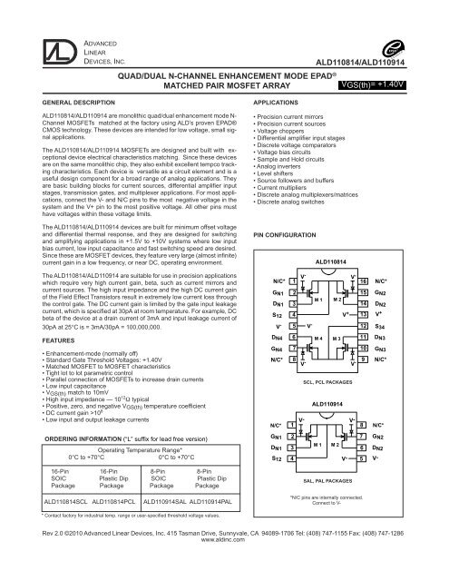
GENERAL DESCRIPTION<br />
ALD110814/ALD110914 are monolithic quad/dual enhancement mode N-<br />
Channel MOSFETs matched at the factory using ALD’s proven <strong>EPAD</strong>®<br />
CMOS technology. These devices are intended for low voltage, small signal<br />
applications.<br />
The ALD110814/ALD110914 MOSFETs are designed and built with exceptional<br />
device electrical characteristics matching. Since these devices<br />
are on the same monolithic chip, they also exhibit excellent tempco tracking<br />
characteristics. Each device is versatile as a circuit element and is a<br />
useful design component for a broad range of analog applications. They<br />
are basic building blocks for current sources, differential amplifier input<br />
stages, transmission gates, and multiplexer applications. For most applications,<br />
connect the V- and N/C pins to the most negative voltage in the<br />
system and the V+ pin to the most positive voltage. All other pins must<br />
have voltages within these voltage limits.<br />
The ALD110814/ALD110914 devices are built for minimum offset voltage<br />
and differential thermal response, and they are designed for switching<br />
and amplifying applications in +1.5V to +10V systems where low input<br />
bias current, low input capacitance and fast switching speed are desired.<br />
Since these are MOSFET devices, they feature very large (almost infinite)<br />
current gain in a low frequency, or near DC, operating environment.<br />
The ALD110814/ALD110914 are suitable for use in precision applications<br />
which require very high current gain, beta, such as current mirrors and<br />
current sources. The high input impedance and the high DC current gain<br />
of the Field Effect Transistors result in extremely low current loss through<br />
the control gate. The DC current gain is limited by the gate input leakage<br />
current, which is specified at 30pA at room temperature. For example, DC<br />
beta of the device at a drain current of 3mA and input leakage current of<br />
30pA at 25°C is = 3mA/30pA = 100,000,000.<br />
FEATURES<br />
• Enhancement-mode (normally off)<br />
• Standard Gate Threshold Voltages: +1.40V<br />
• Matched MOSFET to MOSFET characteristics<br />
• Tight lot to lot parametric control<br />
• Parallel connection of MOSFETs to increase drain currents<br />
• Low input capacitance<br />
• V GS(th) match to 10mV<br />
• High input impedance — 10 12 Ω typical<br />
• Positive, zero, and negative V GS(th) temperature coefficient<br />
• DC current gain >10 8<br />
• Low input and output leakage currents<br />
ORDERING INFORMATION (“L” suffix for lead free version)<br />
Operating Temperature Range*<br />
0°C to +70°C 0°C to +70°C<br />
APPLICATIONS<br />
• Precision current mirrors<br />
• Precision current sources<br />
• Voltage choppers<br />
• Differential amplifier input stages<br />
• Discrete voltage comparators<br />
• Voltage bias circuits<br />
• Sample and Hold circuits<br />
• Analog inverters<br />
• Level shifters<br />
• Source followers and buffers<br />
• Current multipliers<br />
• Discrete analog multiplexers/matrices<br />
• Discrete analog switches<br />
PIN CONFIGURATION<br />
<br />
N/C*<br />
G N1<br />
D N1<br />
1<br />
2<br />
V -<br />
16<br />
15<br />
3<br />
M 1 M 2<br />
14<br />
S 12 4 V + 13<br />
V - 5 12<br />
V - ALD110814<br />
D N4<br />
G N4<br />
6<br />
7<br />
M 4 M 3 11<br />
10<br />
N/C* 8<br />
V - V - 9<br />
N/C*<br />
G N1<br />
D N1<br />
S 12<br />
SCL, PCL PACKAGES<br />
ALD110914<br />
1<br />
2<br />
V-<br />
V-<br />
8<br />
7<br />
3<br />
M 1 M 2<br />
6<br />
4 V- 5<br />
N/C*<br />
G N2<br />
D N2<br />
V +<br />
S 34<br />
D N3<br />
G N3<br />
N/C*<br />
N/C*<br />
G N2<br />
D N2<br />
V - V-<br />
16-Pin 16-Pin 8-Pin 8-Pin<br />
SOIC Plastic Dip SOIC Plastic Dip<br />
Package Package Package Package<br />
SAL, PAL PACKAGES<br />
ALD110814SCL ALD110814PCL<br />
ALD110914SAL ALD110914PAL<br />
*N/C pins are internally connected.<br />
Connect to V-<br />
* Contact factory for industrial temp. range or user-specified threshold voltage values.<br />
Rev 2.0 ©2010 Advanced Linear Devices, Inc. 415 Tasman Drive, Sunnyvale, CA 94089-1706 Tel: (408) 747-1155 Fax: (408) 747-1286<br />
www.aldinc.com
ABSOLUTE MAXIMUM RATINGS<br />
Drain-Source voltage, V DS 10.6V<br />
Gate-Source voltage, V GS 10.6V<br />
Power dissipation<br />
500 mW<br />
Operating temperature range SCL, PCL, SAL, PAL package<br />
0°C to +70°C<br />
Storage temperature range<br />
-65°C to +150°C<br />
Lead temperature, 10 seconds<br />
+260°C<br />
OPERATING ELECTRICAL CHARACTERISTICS<br />
V+ = +5V V- = GND TA = 25°C unless otherwise specified<br />
CAUTION: ESD Sensitive Device. Use static control procedures in ESD controlled environment.<br />
ALD110814 / ALD110914<br />
Parameter Symbol Min Typ Max Unit Test Conditions<br />
Gate Threshold Voltage VGS(th) 1.38 1.40 1.42 V IDS =1µA, VDS = 0.1V<br />
Offset Voltage<br />
VGS(th)1-VGS(th)2 VOS 3 10 mV IDS =1µA<br />
Offset VoltageTempco TC ∆VOS 5 µV/ °C VDS1 = VDS2<br />
GateThreshold Voltage Tempco TC∆VGS(th) -1.7 mV °C ID = 1µA, VDS = 0.1V<br />
0.0 ID = 20µA, VDS = 0.1V<br />
+1.6 ID = 40µA, VDS = 0.1V<br />
On Drain Current IDS (ON) 12.0 mA VGS = +10.6V, VDS = + 5V<br />
3.0 VGS = + 5.4V, VDS = + 5V<br />
Forward Transconductance GFS 1.4 mmho VGS = +5.4V<br />
VDS = +10.4V<br />
Transconductance Mismatch ∆GFS 1.8 %<br />
VGS = + 5.4V<br />
Output Conductance GOS 68 µmho VDS = +10.4V<br />
Drain Source On Resistance RDS (ON) 500 Ω VDS = 0.1V<br />
VGS = +5.6V<br />
Drain Source On Resistance ∆RDS (ON) 0.5 %<br />
Mismatch<br />
Drain Source Breakdown Voltage BVDSX 10 V IDS = 1.0µA<br />
VGS = +0.4V<br />
Drain Source Leakage Current1 IDS (OFF) 10 400 pA VGS = +0.4V<br />
4 nA VDS =5V, TA = 125°C<br />
Gate Leakage Current1 IGSS 3 200 pA VDS = 0V, VGS = 5V<br />
1 nA TA =125°C<br />
Input Capacitance CISS 2.5 pF<br />
Transfer Reverse Capacitance CRSS 0.1 pF<br />
Turn-on Delay Time ton 10 ns V+ = 5V RL= 5KΩ<br />
Turn-off Delay Time toff 10 ns V+ = 5V RL= 5KΩ<br />
Crosstalk 60 dB f = 100KHz<br />
Notes:<br />
1<br />
Consists of junction leakage currents<br />
ALD110814/ALD110914 Advanced Linear Devices 2 of 11
PERFORMANCE CHARACTERISTICS OF <strong>EPAD</strong>® MATCHED PAIR MOSFET FAMILY<br />
ALD1108xx/ALD1109xx/ALD1148xx/ALD1149xx are monolithic<br />
quad/dual N-Channel MOSFETs matched at the factory using ALD’s<br />
proven <strong>EPAD</strong>® CMOS technology. These devices are intended for<br />
low voltage, small signal applications.<br />
ALD’s Electrically Programmable Analog Device (<strong>EPAD</strong>) technology<br />
provides the industry’s only family of matched transistors with<br />
a range of precision threshold values. All members of this family<br />
are designed and actively programmed for exceptional matching of<br />
device electrical characteristics. Threshold values range from -<br />
3.50V Depletion to +3.50V Enhancement devices, including standard<br />
products specified at -3.50V, -1.30V, -0.40V, +0.00V, +0.20V,<br />
+0.40V, +0.80V, +1.40V, and +3.30V. ALD can also provide any<br />
customer desired value between -3.50V and +3.50V. For all these<br />
devices, even the depletion and zero threshold transistors, ALD<br />
<strong>EPAD</strong> technology enables the same well controlled turn-off, subthreshold,<br />
and low leakage characteristics as standard enhancement<br />
mode MOSFETs. With the design and active programming,<br />
even units from different batches and different date of manufacture<br />
have well matched characteristics. As these devices are on the<br />
same monolithic chip, they also exhibit excellent tempco tracking.<br />
This <strong>EPAD</strong> MOSFET Array product family (<strong>EPAD</strong> MOSFET) is available<br />
in the three separate categories, each providing a distinctly<br />
different set of electrical specifications and characteristics. The first<br />
category is the ALD110800/ALD110900 Zero-Threshold mode<br />
<strong>EPAD</strong> MOSFETs. The second category is the ALD1108xx/<br />
ALD1109xx enhancement mode <strong>EPAD</strong> MOSFETs. The third category<br />
is the ALD1148xx/ALD1149xx depletion mode <strong>EPAD</strong><br />
MOSFETs. (The suffix “xx” denotes threshold voltage in 0.1 V steps,<br />
for example, xx=08 denotes 0.80V).<br />
The ALD110800/ALD110900 (quad/dual) are <strong>EPAD</strong> MOSFETs in<br />
which the individual threshold voltage of each MOSFET is fixed at<br />
zero. The threshold voltage is defined as I DS = 1uA @ V DS = 0.1V<br />
when the gate voltage V GS = 0.00V. Zero threshold devices operate<br />
in the enhancement region when operated above threshold voltage<br />
and current level (V GS > 0.00V and I DS > 1uA) and subthreshold<br />
region when operated at or below threshold voltage and current<br />
level (V GS = V GS - V GS(th) , the saturation<br />
current I DS is now given by (approx.):<br />
I DS = u . C OX . W/L . [V GS - V GS(th) ]2<br />
ALD110814/ALD110914 Advanced Linear Devices 3 of 11
PERFORMANCE CHARACTERISTICS OF <strong>EPAD</strong>® MATCHED PAIR MOSFET FAMILY (cont.)<br />
SUB-THRESHOLD REGION OF OPERATION<br />
Low voltage systems, namely those operating at 5V, 3.3V or less,<br />
typically require MOSFETs that have threshold voltage of 1V or<br />
less. The threshold, or turn-on, voltage of the MOSFET is a voltage<br />
below which the MOSFET conduction channel rapidly turns off. For<br />
analog designs, this threshold voltage directly affects the operating<br />
signal voltage range and the operating bias current levels.<br />
At or below threshold voltage, an <strong>EPAD</strong> MOSFET exhibits a turnoff<br />
characteristic in an operating region called the subthreshold region.<br />
This is when the <strong>EPAD</strong> MOSFET conduction channel rapidly<br />
turns off as a function of decreasing applied gate voltage. The conduction<br />
channel induced by the gate voltage on the gate electrode<br />
decreases exponentially and causes the drain current to decrease<br />
exponentially. However, the conduction channel does not shut off<br />
abruptly with decreasing gate voltage, but decreases at a fixed rate<br />
of approximately 116mV per decade of drain current decrease. Thus<br />
if the threshold voltage is +0.20V, for example, the drain current is<br />
1uA at V GS = +0.20V. At V GS = +0.09V, the drain current would<br />
decrease to 0.1uA. Extrapolating from this, the drain current is<br />
0.01uA (10nA) at V GS = -0.03V, 1nA at V GS = -0.14V, and so forth.<br />
This subthreshold characteristic extends all the way down to current<br />
levels below 1nA and is limited by other currents such as junction<br />
leakage currents.<br />
At a drain current to be declared “zero current” by the user, the Vgs<br />
voltage at that zero current can now be estimated. Note that using<br />
the above example, with V GS(th) = +0.20V, the drain current still<br />
hovers around 20nA when the gate is at zero volt, or ground.<br />
LOW POWER AND NANOPOWER<br />
When supply voltages decrease, the power consumption of a given<br />
load resistor decreases as the square of the supply voltage. So<br />
one of the benefits in reducing supply voltage is to reduce power<br />
consumption. While decreasing power supply voltages and power<br />
consumption go hand-in-hand with decreasing useful AC bandwidth<br />
and at the same time increases noise effects in the circuit, a circuit<br />
designer can make the necessary tradeoffs and adjustments in any<br />
given circuit design and bias the circuit accordingly.<br />
With <strong>EPAD</strong> MOSFETs, a circuit that performs a specific function<br />
can be designed so that power consumption can be minimized. In<br />
some cases, these circuits operate in low power mode where the<br />
power consumed is measure in micro-watts. In other cases, power<br />
dissipation can be reduced to nano-watt region and still provide a<br />
useful and controlled circuit function operation.<br />
ZERO TEMPERATURE COEFFICIENT (ZTC) OPERATION<br />
For an <strong>EPAD</strong> MOSFET in this product family, there exist operating<br />
points where the various factors that cause the current to increase<br />
as a function of temperature balance out those that cause the current<br />
to decrease, thereby canceling each other, and resulting in net<br />
temperature coefficient of near zero. One of this temperature stable<br />
operating point is obtained by a ZTC voltage bias condition, which<br />
is 0.55V above a threshold voltage when V GS = V DS , resulting in a<br />
temperature stable current level of about 68uA. For other ZTC operating<br />
points, see ZTC characteristics.<br />
PERFORMANCE CHARACTERISTICS<br />
Performance characteristics of the <strong>EPAD</strong> MOSFET product family<br />
are shown in the following graphs. In general, the threshold voltage<br />
shift for each member of the product family causes other affected<br />
electrical characteristics to shift with an equivalent linear shift in<br />
V GS(th) bias voltage. This linear shift in V GS causes the subthreshold<br />
I-V curves to shift linearly as well. Accordingly, the subthreshold<br />
operating current can be determined by calculating the gate voltage<br />
drop relative from its threshold voltage, V GS(th) .<br />
RDS(ON) AT VGS=GROUND<br />
Several of the <strong>EPAD</strong> MOSFETs produce a fixed resistance when<br />
their gate is grounded. For ALD110800, the drain current at V DS =<br />
0.1V is at 1uA at V GS = 0.0V. Thus just by grounding the gate of the<br />
ALD110800, a resistor with R DS(ON) = ~100KOhm is produced.<br />
When an ALD114804 gate is grounded, the drain current I DS = 18.5<br />
uA@ V DS = 0.1V, producing R DS(ON) = 5.4KOhm. Similarly,<br />
ALD114813 and ALD114835 produces 77uA and 185uA, respectively,<br />
at V GS = 0.0V, producing R DS(ON) values of 1.3KOhm and<br />
540Ohm, respectively.<br />
MATCHING CHARACTERISTICS<br />
A key benefit of using matched-pair <strong>EPAD</strong> MOSFET is to maintain<br />
temperature tracking. In general, for <strong>EPAD</strong> MOSFET matched pair<br />
devices, one device of the matched pair has gate leakage currents,<br />
junction temperature effects, and drain current temperature coefficient<br />
as a function of bias voltage that cancel out similar effects of<br />
the other device, resulting in a temperature stable circuit. As mentioned<br />
earlier, this temperature stability can be further enhanced by<br />
biasing the matched-pairs at Zero Tempco (ZTC) point, even though<br />
that could require special circuit configuration and power consumption<br />
design consideration.<br />
ALD110814/ALD110914 Advanced Linear Devices 4 of 11
TYPICAL PERFORMANCE CHARACTERISTICS<br />
DRAIN SOURCE ON CURRENT<br />
(mA)<br />
OUTPUT CHARACTERISTICS<br />
5<br />
T A = +25°C<br />
V GS -V GS(TH) =+5V<br />
4<br />
V GS -V GS(TH) =+4V<br />
3<br />
V GS -V GS(TH) =+3V<br />
2<br />
V GS -V GS(TH) =+2V<br />
1<br />
V GS -V GS(TH) =+1V<br />
0<br />
0 2 4 6 8 10<br />
DRAIN-SOURCE ON VOLTAGE (V)<br />
DRAIN-SOURCE ON RESISTANCE <br />
(Ω)<br />
2500<br />
2000<br />
1500<br />
1000<br />
500<br />
0<br />
DRAIN-SOURCE ON RESISTANCE <br />
vs. DRAIN-SOURCE ON CURRENT<br />
<br />
<br />
TA = 25°C<br />
V GS = V GS(TH) +4V<br />
V GS = V GS(TH) +6V<br />
100<br />
10 1000 10000<br />
DRAIN-SOURCE ON CURRENT (µA)<br />
DRAIN- SOURCE ON CURRENT<br />
(mA )<br />
20<br />
15<br />
10<br />
5<br />
0<br />
FORWARD TRANSFER CHARACTERISTICS<br />
<br />
T A = 25°C<br />
V DS = +10V<br />
VGS(TH) = 0.0V<br />
VGS(TH) = +0.2V<br />
VGS(TH) = -0.4V<br />
VGS(TH) = -1.3V<br />
-4 -2 0 2 4 6 8 10<br />
GATE-SOURCE VOLTAGE (V)<br />
VGS(TH) = -3.5V<br />
VGS(TH) = +1.4V<br />
VGS(TH) = +0.8V<br />
TRANSCONDUCTANCE <br />
(mA/V)<br />
2.5<br />
2.0<br />
1.5<br />
1.0<br />
0.5<br />
0<br />
TRANSCONDUCTANCE vs.<br />
AMBIENT TEMPERATURE<br />
<br />
-50 -25 0 25 50 75 100 125<br />
AMBIENT TEMPERATURE (°C)<br />
DRAIN-SOURCE ON CURRENT<br />
(nA)<br />
<br />
100000<br />
10000<br />
1000<br />
100<br />
10<br />
1<br />
SUBTHRESHOLD FORWARD TRANSFER <br />
CHARACTERISTICS<br />
<br />
T A = +25°C<br />
V DS =+0.1V<br />
V GS(TH) =-1.3V<br />
V GS(TH) =0.0V<br />
0.1 V GS(TH) =-3.5V<br />
V GS(TH) =+0.2V<br />
V GS(TH) =+0.8V<br />
0.01<br />
-4 -3 -2 -1 0 1 2<br />
GATE-SOURCE VOLTAGE (V)<br />
V GS(TH) =-0.4V<br />
V GS(TH) =+1.4V<br />
DRAIN-SOURCE ON CURRENT<br />
(nA)<br />
1000<br />
100<br />
10<br />
1<br />
0.1<br />
SUBTHRESHOLD FORWARD TRANSFER<br />
CHARACTERISTICS<br />
V DS =0.1V<br />
Slope ~ = 110mV/decade<br />
0.01<br />
V GS(th) V GS(th) V GS(th) V GS(th) V GS(th) V GS(th)<br />
-0.5 -0.4 -0.3 -0.2 -0.1<br />
GATE-SOURCE VOLTAGE (V)<br />
ALD110814/ALD110914 Advanced Linear Devices 5 of 11
TYPICAL PERFORMANCE CHARACTERISTICS<br />
DRAIN SOURCE ON CURRENT<br />
(mA)<br />
<br />
DRAIN-SOURCE ON CURRENT<br />
(µA)<br />
<br />
5<br />
4<br />
3<br />
2<br />
1<br />
0<br />
DRAIN SOURCE ON CURRENT, BIAS <br />
CURRENT vs. AMBIENT TEMPERATURE<br />
-55°C<br />
-25°C<br />
0°C<br />
70°C 125°C<br />
VGS(TH)-1 VGS(TH) VGS(TH)+1 VGS(TH)+2 VGS(TH)+3 VGS(TH)+4<br />
GATE AND DRAIN SOURCE VOLTAGE<br />
(VGS = VDS) (V) <br />
<br />
DRAIN-SOURCE ON CURRENT vs. ON RESISTANCE<br />
<br />
100000<br />
10000<br />
1000<br />
100<br />
10<br />
1<br />
0.1<br />
VDS =+10V T A = 25°C<br />
VGS=-4.0V to +5.4V<br />
V DS =+0.1V<br />
0.01<br />
0.1 1 10 100 1000<br />
ON RESISTANCE (KΩ)<br />
V DS =+5V<br />
V DS =+1V<br />
10000<br />
DRAIN SOURCE ON CURRENT<br />
( µA)<br />
GATE SOURCE VOLTAGE (V)<br />
100<br />
50<br />
V GS(TH) +4<br />
V GS(TH) +3<br />
V GS(TH) +2<br />
V GS(TH) +1<br />
V GS(TH)<br />
V GS(TH) -1<br />
DRAIN SOURCE ON CURRENT, BIAS<br />
CURRENT vs. AMBIENT TEMPERATURE<br />
Zero Temperature<br />
Coefficient (ZTC)<br />
125°C<br />
- 25°C<br />
0<br />
V GS(TH) V GS(TH) V GS(TH) V GS(TH) V GS(TH) V GS(TH)<br />
+0.0 +0.2 +0.4 +0.6 +0.8 +1.0<br />
GATE AND DRAIN SOURCE VOLTAGE<br />
(VGS = VDS) (V)<br />
GATE SOURCE VOLTAGE vs. DRAIN<br />
SOURCE ON CURRENT<br />
V GS<br />
D<br />
S<br />
V DS<br />
I DS(ON)<br />
V DS = 0.5V<br />
T A = +25°C<br />
V DS = 0.5V<br />
T A = +125°C<br />
DRAIN SOURCE ON CURRENT (µA)<br />
V DS = 5V<br />
T A = +25°C<br />
V DS = 5V V DS = R ON • I DS(ON)<br />
T A = +125°C<br />
0.1 1 10 100 1000 10000<br />
DRAIN SOURCE ON CURRENT<br />
(mA)<br />
5<br />
4<br />
3<br />
2<br />
1<br />
0<br />
DRAIN SOURCE ON CURRENT vs.<br />
OUTPUT VOLTAGE<br />
TA = 25°C<br />
V DS = +10V<br />
V DS = +5V<br />
V DS = +1V<br />
OFFSET VOLTAGE (mV)<br />
4<br />
3<br />
2<br />
1<br />
0<br />
-1<br />
-2<br />
-3<br />
-4<br />
OFFSET VOLTAGE vs.<br />
AMBIENT TEMPERATURE<br />
REPRESENTATIVE UNITS<br />
VGS(TH) V GS(TH) +1 VGS(TH)+2 V GS(TH) +3 VGS(TH)+4 VGS(TH)+5<br />
-50 -25 0 25 50 75 100 125<br />
OUTPUT VOLTAGE (V)<br />
AMBIENT TEMPERATURE (°C)<br />
GATE LEAKAGE CURRENT (pA)<br />
<br />
<br />
600<br />
500<br />
400<br />
300<br />
200<br />
100<br />
GATE LEAKAGE CURRENT <br />
vs. AMBIENT TEMPERATURE<br />
I GSS<br />
0<br />
-50 -25 0 25 50 75 100 125<br />
AMBIENT TEMPERATURE (°C)<br />
GATE SOURCE VOLTAGE <br />
vs. ON - RESISTANCE<br />
<br />
D V DS<br />
0.1 1 10 100 1000 10000<br />
ALD110814/ALD110914 Advanced Linear Devices 6 of 11<br />
GATE SOURCE VOLTAGE (V)<br />
V GS(TH) +4<br />
V GS(TH) +3<br />
V GS(TH) +2<br />
V GS(TH) +1<br />
V GS(TH)<br />
+25°C<br />
+125°C<br />
V GS<br />
ON - RESISTANCE (KΩ)<br />
I DS(ON)<br />
S<br />
0.0V ≤ V DS ≤ 5.0V
TYPICAL PERFORMANCE CHARACTERISTICS<br />
DRAIN- GATE DIODE CONNECTED <br />
VOLTAGE TEMPCO (mV/ °C )<br />
DRAIN - GATE DIODE CONNECTED VOLTAGE<br />
TEMPCO vs. DRAIN SOURCE ON CURRENT<br />
5<br />
<br />
2.5<br />
0<br />
-2.5<br />
-5<br />
-55°C ≤ T A ≤ +125°C<br />
1 10 100 1000<br />
DRAIN SOURCE ON CURRENT (µA)<br />
TRANSCONDUCTANCE<br />
( mΩ -1 )<br />
<br />
1.6<br />
1.2<br />
0.8<br />
0.4<br />
0.0<br />
TRANSFER CHARACTERISTICS<br />
<br />
T A = 25°C<br />
V DS = +10V<br />
VGS(TH) = 0.0V<br />
VGS(TH) = +0.2V<br />
VGS(TH) = -0.4V<br />
VGS(TH) = -3.5V<br />
VGS(TH) = -1.3V<br />
VGS(TH) = +1.4V<br />
VGS(TH) = +0.8V<br />
-4 -2 0 2 4 6 8 10<br />
GATE-SOURCE VOLTAGE (V)<br />
GATE-SOURCE VOLTAGE - THRESHOLD<br />
VOLTAGE (V)<br />
<br />
ZERO TEMPERETURE COEFFICIENT CHARACTERISTIC<br />
0.6<br />
0.5<br />
0.3<br />
0.2<br />
V GS(TH) =-3.5V<br />
VGS(TH)=-1.3V, -0.4V, 0.0V, +0.2V, +0.8V, +1.4V<br />
0.0<br />
0.1 0.2 0.5 1.0 2.0 5.0<br />
DRAIN-SOURCE ON VOLTAGE (V)<br />
<br />
GATE-SOURCE VOLTAGE (V)<br />
<br />
2.5<br />
2.0<br />
1.5<br />
1.0<br />
SUBTHRESHOLD CHARACTERISTICS <br />
<br />
<br />
<br />
25°C<br />
0.5<br />
V GS(th) = 0.4V<br />
<br />
0.0<br />
55°C VGS(th) = 0.2V<br />
-0.5<br />
<br />
100000 10000 1000 100 10 1 0.1<br />
DRAIN -SOURCE CURRENT (nA)<br />
TARNCONDUCTANCE<br />
( mΩ -1 )<br />
<br />
TRANCONDUCTANCE vs. DRAIN-SOURCE <br />
ON CURRENT<br />
1.2<br />
T A = 25°C<br />
V DS = +10V<br />
0.9<br />
0.6<br />
0.3<br />
0.0<br />
0<br />
2 4 6 8 10<br />
<br />
DRAIN -SOURCE ON CURRENT(mA)<br />
THRESHOLD VOTAGE<br />
(V)<br />
4.0<br />
3.0<br />
2.0<br />
1.0<br />
0<br />
V t = 0.0V<br />
THRESHOLD VOLTAGE vs.<br />
AMBIENT TEMPERATURE<br />
V DS = +0.1V I D = 1.0 µA<br />
V t = 0.2V<br />
AMBIENT TEMPERATURE (°C)<br />
V t = 1.4V<br />
V t = 0.8V<br />
V t = 0.4V<br />
-50 -25 0 25 50 75 100 125<br />
GATE-SOURCE VOLTAGE - THRESHOLD <br />
VOLTAGE<br />
<br />
(V)<br />
V GS - VGS(th)<br />
<br />
0.3<br />
0.2<br />
0.1<br />
0<br />
NORMALIZED SUBTHRESHOLD <br />
CHARACTERISTICS RELATIVE<br />
GATE THRESHOLD VOLTAGE<br />
<br />
-0.1<br />
25°C<br />
-0.2<br />
55°C<br />
-0.3<br />
-0.4<br />
10000 1000 100 10 1 0.1<br />
DRAIN-SOURCE CURRENT (nA)<br />
<br />
V D = 0.1V<br />
ALD110814/ALD110914 Advanced Linear Devices 7 of 11<br />
THRESHOLD VOLTAGE<br />
(V)<br />
2.0<br />
1.0<br />
0.0<br />
-1.0<br />
-2.0<br />
-3.0<br />
-4.0<br />
THRESHOLD VOLTAGES<br />
vs. AMBIENT TEMPERATURES<br />
V GS(th) = 0.0V<br />
V GS(th) = -0.4V<br />
V GS(th) = -1.3V<br />
V GS(th) = -3.5V<br />
-25 25 75 125<br />
AMBIENT TEMPERATURE ( O C)<br />
I DS = +1µA<br />
V DS = +0.1V
SOIC-16 PACKAGE DRAWING<br />
16 Pin Plastic SOIC Package<br />
E<br />
Millimeters<br />
Inches<br />
Dim<br />
Min Max Min Max<br />
S (45°)<br />
A<br />
A 1<br />
1.35<br />
0.10<br />
1.75<br />
0.25<br />
0.053<br />
0.004<br />
0.069<br />
0.010<br />
b<br />
0.35<br />
0.45<br />
0.014<br />
0.018<br />
C<br />
0.18<br />
0.25<br />
0.007<br />
0.010<br />
D-16<br />
9.80<br />
10.00<br />
0.385<br />
0.394<br />
D<br />
E<br />
e<br />
3.50 4.05 0.140 0.160<br />
1.27 BSC 0.050 BSC<br />
H<br />
5.70<br />
6.30<br />
0.224<br />
0.248<br />
A<br />
L<br />
ø<br />
0.60<br />
0°<br />
0.937<br />
8°<br />
0.024<br />
0°<br />
0.037<br />
8°<br />
e<br />
A 1<br />
b<br />
S<br />
0.25<br />
0.50<br />
0.010<br />
<br />
0.020<br />
S (45°)<br />
H<br />
C<br />
L<br />
ø<br />
ALD110814/ALD110914 Advanced Linear Devices 8 of 11
PDIP-16 PACKAGE DRAWING<br />
16 Pin Plastic DIP Package<br />
E<br />
E1<br />
Millimeters<br />
Inches<br />
Dim<br />
Min Max Min Max<br />
A<br />
3.81<br />
5.08<br />
0.105<br />
0.200<br />
A 1<br />
0.38<br />
1.27<br />
0.015<br />
0.050<br />
A 2<br />
1.27<br />
2.03<br />
0.050<br />
0.080<br />
b<br />
0.89<br />
1.65<br />
0.035<br />
0.065<br />
b 1<br />
0.38<br />
0.51<br />
0.015<br />
0.020<br />
S<br />
D<br />
c<br />
D-16<br />
E<br />
0.20<br />
18.93<br />
5.59<br />
0.30<br />
21.33<br />
7.11<br />
0.008<br />
0.745<br />
0.220<br />
0.012<br />
0.840<br />
0.280<br />
E 1<br />
7.62<br />
8.26<br />
0.300<br />
0.325<br />
b<br />
e<br />
A 2<br />
A 1<br />
L<br />
A<br />
e<br />
e 1<br />
L<br />
S-16<br />
2.29<br />
7.37<br />
2.79<br />
0.38<br />
2.79<br />
7.87<br />
3.81<br />
1.52<br />
0.090<br />
0.290<br />
0.110<br />
0.015<br />
0.110<br />
0.310<br />
0.150<br />
0.060<br />
ø<br />
0°<br />
15°<br />
0°<br />
15°<br />
b 1<br />
c<br />
e 1<br />
ø<br />
ALD110814/ALD110914 Advanced Linear Devices 9 of 11
SOIC-8 PACKAGE DRAWING<br />
8 Pin Plastic SOIC Package<br />
E<br />
Millimeters<br />
Inches<br />
S (45°)<br />
D<br />
Dim<br />
A<br />
A 1<br />
b<br />
C<br />
D-8<br />
E<br />
Min Max Min Max<br />
1.35 1.75 0.053 0.069<br />
0.10 0.25 0.004 0.010<br />
0.35 0.45 0.014 0.018<br />
0.18 0.25 0.007 0.010<br />
4.69 5.00 0.185 0.196<br />
3.50 4.05 0.140 0.160<br />
e<br />
1.27 BSC 0.050 BSC<br />
e<br />
b<br />
A<br />
A 1<br />
H<br />
L<br />
ø<br />
S<br />
5.70<br />
0.60<br />
0°<br />
0.25<br />
6.30<br />
0.937<br />
8°<br />
0.50<br />
0.224<br />
0.024<br />
0°<br />
0.010<br />
<br />
0.248<br />
0.037<br />
8°<br />
0.020<br />
S (45°)<br />
H<br />
C<br />
L<br />
ø<br />
ALD110814/ALD110914 Advanced Linear Devices 10 of 11
PDIP-8 PACKAGE DRAWING<br />
8 Pin Plastic DIP Package<br />
E<br />
E1<br />
Millimeters<br />
Inches<br />
Dim<br />
A<br />
Min Max Min Max<br />
3.81 5.08 0.105 0.200<br />
A 1<br />
0.38<br />
1.27<br />
0.015<br />
0.050<br />
A 2<br />
1.27<br />
2.03<br />
0.050<br />
0.080<br />
b<br />
0.89<br />
1.65<br />
0.035<br />
0.065<br />
S<br />
D<br />
b 1<br />
c<br />
D-8<br />
0.38<br />
0.20<br />
9.40<br />
0.51<br />
0.30<br />
11.68<br />
0.015<br />
0.008<br />
0.370<br />
0.020<br />
0.012<br />
0.460<br />
E<br />
5.59<br />
7.11<br />
0.220<br />
0.280<br />
b<br />
b 1<br />
e<br />
A2<br />
A 1<br />
L<br />
A<br />
E 1<br />
e<br />
e 1<br />
L<br />
S-8<br />
ø<br />
7.62<br />
2.29<br />
7.37<br />
2.79<br />
1.02<br />
0°<br />
8.26<br />
2.79<br />
7.87<br />
3.81<br />
2.03<br />
15°<br />
0.300<br />
0.090<br />
0.290<br />
0.110<br />
0.040<br />
0°<br />
0.325<br />
0.110<br />
0.310<br />
0.150<br />
0.080<br />
15°<br />
c<br />
e 1<br />
ø<br />
ALD110814/ALD110914 Advanced Linear Devices 11 of 11