PIC24F Family Reference Manual, Sect. 6 Oscillator - Microchip
PIC24F Family Reference Manual, Sect. 6 Oscillator - Microchip
PIC24F Family Reference Manual, Sect. 6 Oscillator - Microchip

Create successful ePaper yourself
Turn your PDF publications into a flip-book with our unique Google optimized e-Paper software.
6<br />
<strong>Sect</strong>ion 6. <strong>Oscillator</strong><br />
<strong>Oscillator</strong><br />
HIGHLIGHTS<br />
This section of the manual contains the following major topics:<br />
6.1 Introduction .................................................................................................................... 6-2<br />
6.2 CPU Clocking Scheme .................................................................................................. 6-3<br />
6.3 <strong>Oscillator</strong> Configuration.................................................................................................. 6-3<br />
6.4 Control Registers ........................................................................................................... 6-5<br />
6.5 Primary <strong>Oscillator</strong> (POSC) ........................................................................................... 6-10<br />
6.6 Phase Locked Loop (PLL) ........................................................................................... 6-14<br />
6.7 Low-Power Secondary <strong>Oscillator</strong> (SOSC) ................................................................... 6-15<br />
6.8 Internal Fast RC <strong>Oscillator</strong> (FRC) ................................................................................ 6-16<br />
6.9 Internal Low-Power RC <strong>Oscillator</strong> (LPRC)................................................................... 6-16<br />
6.10 Fail-Safe Clock Monitor (FSCM) .................................................................................. 6-17<br />
6.11 Clock Switching Operation........................................................................................... 6-18<br />
6.12 Two-Speed Start-up ..................................................................................................... 6-21<br />
6.13 AC Electrical Specifications ......................................................................................... 6-22<br />
6.14 Design Tips .................................................................................................................. 6-23<br />
6.16 Related Application Notes............................................................................................ 6-25<br />
6.17 Revision History ........................................................................................................... 6-26<br />
© 2006 <strong>Microchip</strong> Technology Inc. Advance Information DS39700A-page 6-1
<strong>PIC24F</strong> <strong>Family</strong> <strong>Reference</strong> <strong>Manual</strong><br />
6.1 INTRODUCTION<br />
This section describes the <strong>PIC24F</strong> oscillator system and its operation. The <strong>PIC24F</strong> oscillator<br />
system has the following modules and features:<br />
• A total of four external and internal oscillator options as clock sources, providing<br />
11 different clock modes<br />
• On-chip 4x PLL to boost internal operating frequency on select internal and external<br />
oscillator sources<br />
• Software-controllable switching between various clock sources<br />
• Software-controllable postscaler for selective clocking of CPU for system power savings<br />
• A Fail-Safe Clock Monitor (FSCM) that detects clock failure and permits safe application<br />
recovery or shutdown<br />
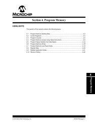
A simplified diagram of the oscillator system is shown in Figure 6-1.<br />
Figure 6-1:<br />
<strong>PIC24F</strong> <strong>Family</strong> Clock Diagram<br />
Primary <strong>Oscillator</strong><br />
<strong>PIC24F</strong> <strong>Family</strong><br />
CLKO<br />
OSC2<br />
XT, HS, EC<br />
CLKDIV<br />
OSC1<br />
8 MHz<br />
4 MHz<br />
4 x PLL<br />
XTPLL, HSPLL,<br />
ECPLL, FRCPLL<br />
Postscaler<br />
CPU<br />
FRC<br />
<strong>Oscillator</strong><br />
8 MHz<br />
(Nominal)<br />
Postscaler<br />
FRCDIV<br />
Peripherals<br />
OSCTUN<br />
CLKDIV<br />
FRC<br />
LPRC<br />
<strong>Oscillator</strong><br />
31 kHz (Nominal)<br />
LPRC<br />
Secondary <strong>Oscillator</strong><br />
SOSCO<br />
SOSCI<br />
SOSCEN<br />
SOSC<br />
Clock Control Logic<br />
Fail-Safe<br />
Clock<br />
Monitor<br />
WDT, PWRT<br />
Timer1, RTCC<br />
DS39700A-page 6-2 Advance Information © 2006 <strong>Microchip</strong> Technology Inc.
6.2 CPU CLOCKING SCHEME<br />
<strong>Sect</strong>ion 6. <strong>Oscillator</strong><br />
The system clock source can be provided by one of four sources:<br />
• Primary <strong>Oscillator</strong> (POSC) on the OSC1 and OSC2 pins<br />
• Secondary <strong>Oscillator</strong> (SOSC) on the SOSCI and SOSCO pins<br />
• Internal Fast RC <strong>Oscillator</strong> (FRC)<br />
• Internal Low-Power RC <strong>Oscillator</strong> (LPRC)<br />
The Primary <strong>Oscillator</strong> and FRC sources have the option of using the internal 4x PLL. The<br />
frequency of the FRC clock source can optionally be reduced by the programmable clock divider.<br />
The selected clock source generates the processor and peripheral clock sources.<br />
The processor clock source is divided by two to produce the internal instruction cycle clock, FCY.<br />
In this document, the instruction cycle clock is also denoted by FOSC/2. The timing diagram in<br />
Figure 6-2 shows the relationship between the processor clock source and instruction execution.<br />
The internal instruction cycle clock, FOSC/2, can be provided on the OSC2 I/O pin for some<br />
operating modes of the Primary <strong>Oscillator</strong>.<br />
6<br />
<strong>Oscillator</strong><br />
Figure 6-2:<br />
Clock/Instruction Cycle Timing<br />
TCY<br />
FOSC<br />
FCY<br />
PC<br />
PC PC + 2 PC + 4<br />
Fetch INST (PC)<br />
Execute INST (PC – 2) Fetch INST (PC + 2)<br />
Execute INST (PC) Fetch INST (PC + 4)<br />
Execute INST (PC + 2)<br />
6.3 OSCILLATOR CONFIGURATION<br />
The oscillator source (and operating mode) that is used at a device Power-on Reset event is<br />
selected using Configuration bit settings. The oscillator Configuration bit settings are in the<br />
Configuration registers located in the program memory (refer to the specific product data sheet for<br />
further details). The Primary <strong>Oscillator</strong> Configuration bits, POSCMD1:POSCMD0<br />
(Configuration Word 2), and oscillator Configuration bits, FNOSC2:FNOSC0<br />
(Configuration Word 2), select the oscillator source that is used at a Power-on Reset. The<br />
FRC oscillator with Postscaler (FRCDIV) is the default (unprogrammed) selection. The Secondary<br />
<strong>Oscillator</strong>, or one of the internal oscillators, may be chosen by programming these bit locations.<br />
The Configuration bits allow users to choose between 11 different clock modes, shown in<br />
Table 6-1.<br />
© 2006 <strong>Microchip</strong> Technology Inc. Advance Information DS39700A-page 6-3
<strong>PIC24F</strong> <strong>Family</strong> <strong>Reference</strong> <strong>Manual</strong><br />
Table 6-1:<br />
<strong>Oscillator</strong> Mode<br />
Configuration Bit Values for Clock Selection<br />
<strong>Oscillator</strong><br />
Source<br />
POSCMD1:<br />
POSCMD0<br />
6.3.1 Clock Switching Mode Configuration Bits<br />
FNOSC2:<br />
FNOSC0<br />
The FCKSM Configuration bits (Configuration Word 2) are used to jointly configure device<br />
clock switching and the Fail-Safe Clock Monitor (FSCM). Clock switching is enabled only when<br />
FCKSM1 is programmed (‘0’). The FSCM is enabled only when FCKSM1:FCKSM0 are both<br />
programmed (‘00’).<br />
6.3.2 OSC1 and OSC2 Pin Functions in Non-Crystal Modes<br />
Note<br />
Fast RC <strong>Oscillator</strong> with<br />
Internal xx 111 1, 2<br />
Postscaler (FRCDIV)<br />
(Reserved) Internal xx 110 1<br />
Low-Power RC <strong>Oscillator</strong> Internal xx 101 1<br />
(LPRC)<br />
Secondary (Timer1) <strong>Oscillator</strong> Secondary xx 100 1<br />
(SOSC)<br />
Primary <strong>Oscillator</strong> (HS) with Primary 10 011<br />
PLL Module (HSPLL)<br />
Primary <strong>Oscillator</strong> (XT) with Primary 01 011<br />
PLL Module (XTPLL)<br />
Primary <strong>Oscillator</strong> (EC) with Primary 00 011<br />
PLL Module (ECPLL)<br />
Primary <strong>Oscillator</strong> (HS) Primary 10 010<br />
Primary <strong>Oscillator</strong> (XT) Primary 01 010<br />
Primary <strong>Oscillator</strong> (EC) Primary 00 010<br />
Fast RC <strong>Oscillator</strong> with PLL Internal xx 001 1<br />
Module (FRCPLL)<br />
Fast RC <strong>Oscillator</strong> (FRC) Internal xx 000 1<br />
Note 1: OSC2 pin function is determined by the OSCIOFCN Configuration bit.<br />
2: Default oscillator mode for an unprogrammed (erased) device.<br />
When the Primary <strong>Oscillator</strong> on OSC1 and OSC2 is not configured as the clock source<br />
(POSCMD1:POSCMD0 = 11), the OSC1 pin is automatically reconfigured as a digital I/O. In this<br />
configuration, as well as when the Primary <strong>Oscillator</strong> is configured for EC mode<br />
(POSCMD1:POSCMD0 = 00), the OSC2 pin can also be configured as a digital I/O by<br />
programming the OSCIOFCN Configuration bit (Configuration Word 2).<br />
When OSCIOFCN is unprogrammed (‘1’), a FOSC/2 clock output is available on OSC2 for testing<br />
or synchronization purposes. With OSCIOFCN programmed (‘0’), the OSC2 pin becomes a<br />
general purpose I/O pin. In both of these configurations, the feedback device between OSC1 and<br />
OSC2 is turned off to save current.<br />
DS39700A-page 6-4 Advance Information © 2006 <strong>Microchip</strong> Technology Inc.
6.4 CONTROL REGISTERS<br />
<strong>Sect</strong>ion 6. <strong>Oscillator</strong><br />
The operation of the oscillator is controlled by three Special Function Registers:<br />
• OSCCON<br />
• CLKDIV<br />
• OSCTUN<br />
6.4.1 <strong>Oscillator</strong> Control Register (OSCCON)<br />
The OSCCON register (Register 6-1) is the main control register for the oscillator. It controls<br />
clock source switching and allows the monitoring of clock sources.<br />
The COSC status bits are read-only bits that indicate the current oscillator source the device is<br />
operating from. The COSC bits default to the Internal Fast RC <strong>Oscillator</strong> with Postscaler<br />
(FRCDIV), configured for 4 MHz, on a Power-on Reset and Master Clear Reset. A clock switch<br />
will automatically be performed to the new oscillator source selected by the FNOSC Configuration<br />
bits (Configuration Word 2). The COSC bits will change to indicate the new oscillator<br />
source at the end of a clock switch operation.<br />
The NOSC status bits select the clock source for the next clock switch operation. On Power-on<br />
Reset and Master Clear Resets, these bits automatically select the oscillator source defined by<br />
the FNOSC Configuration bits. These bits can be modified by software.<br />
6<br />
<strong>Oscillator</strong><br />
Note:<br />
An unlock sequence must be performed before writing to OSCCON. Refer to<br />
<strong>Sect</strong>ion 6.11.2 “<strong>Oscillator</strong> Switching Sequence” for more information.<br />
Setting the CLKLOCK bit (OSCCON) prevents clock switching if the FCKSM1 Configuration<br />
bit is set. If the FCKSM1 bit is clear, the CLKLOCK bit state is ignored and clock switching can<br />
occur.<br />
The LOCK status bit (OSCCON) is read-only and indicates the status of the PLL circuit. It is<br />
set when the PLL achieves a frequency lock, and is reset when a valid clock switching sequence<br />
is initiated. It reads as ‘0’ whenever the PLL is not used as part of the current clock source.<br />
The CF status bit (OSCCON) is a readable/clearable status bit that indicates a clock failure.<br />
It is reset whenever a valid clock switch occurs.<br />
The SOSCEN control bit (OSCCON) is used to enable or disable the 32 kHz SOSC crystal<br />
oscillator.<br />
The OSWEN control bit (OSCCON) is used to initiate a clock switch operation. OSWEN is<br />
cleared automatically after a successful clock switch, any redundant clock switch, and by the<br />
FSCM module after the switch to the FRC has completed.<br />
© 2006 <strong>Microchip</strong> Technology Inc. Advance Information DS39700A-page 6-5
<strong>PIC24F</strong> <strong>Family</strong> <strong>Reference</strong> <strong>Manual</strong><br />
Register 6-1:<br />
OSCCON: <strong>Oscillator</strong> Control Register<br />
U-0 R-0 R-0 R-0 U-0 R/W-x (1) R/W-x (1) R/W-x (1)<br />
— COSC2 COSC1 COSC0 — NOSC2 NOSC1 NOSC0<br />
bit 15 bit 8<br />
R/SO-0 U-0 R-0 (2) U-0 R/CO-0 U-0 R/W-0 R/W-0<br />
CLKLOCK — LOCK — CF — SOSCEN OSWEN<br />
bit 7 bit 0<br />
Legend: U = Unimplemented bit, read as ‘0’<br />
R = Readable bit W = Writable bit CO = Clearable Only bit SO = Settable Only bit<br />
- n = Value at all Resets ‘1’ = Bit is set ‘0’ = Bit is cleared x = Bit is unknown<br />
bit 15 Unimplemented: Read as ‘0’<br />
bit 14-12 COSC2:COSC0: Current <strong>Oscillator</strong> Selection bits<br />
111 = Fast RC <strong>Oscillator</strong> with Postscaler (FRCDIV)<br />
110 = Reserved<br />
101 = Low-Power RC <strong>Oscillator</strong> (LPRC)<br />
100 = Secondary <strong>Oscillator</strong> (SOSC)<br />
011 = Primary <strong>Oscillator</strong> with PLL module (XTPLL, HSPLL or ECPLL)<br />
010 = Primary <strong>Oscillator</strong> (XT, HS or EC)<br />
001 = Fast RC <strong>Oscillator</strong> with PLL module via Postscaler (FRCPLL) (3)<br />
000 = Fast RC <strong>Oscillator</strong> (FRC)<br />
bit 11 Unimplemented: Read as ‘0’<br />
bit 10-8 NOSC2:NOSC0: New <strong>Oscillator</strong> Selection bits<br />
111 = Fast RC <strong>Oscillator</strong> with Postscaler (FRCDIV)<br />
110 = Reserved<br />
101 = Low-Power RC <strong>Oscillator</strong> (LPRC)<br />
100 = Secondary <strong>Oscillator</strong> (SOSC)<br />
011 = Primary <strong>Oscillator</strong> with PLL module (XTPLL, HSPLL or ECPLL)<br />
010 = Primary <strong>Oscillator</strong> (XT, HS or EC)<br />
001 = Fast RC <strong>Oscillator</strong> with PLL module via Postscaler (FRCPLL) (3)<br />
000 = Fast RC <strong>Oscillator</strong> (FRC)<br />
bit 7 CLKLOCK: Clock Selection Lock Enable bit<br />
If FSCM is enabled (FCKSM1 = 1):<br />
1 = Clock and PLL selections are locked.<br />
0 = Clock and PLL selections are not locked and may be modified by setting the OSWEN bit<br />
If FSCM is disabled (FCKSM1 = 0):<br />
Clock and PLL selections are never locked and may be modified by setting the OSWEN bit.<br />
bit 6 Unimplemented: Read as ‘0’<br />
bit 5 LOCK: PLL Lock Status bit<br />
1 = PLL module is in lock or PLL module start-up timer is satisfied<br />
0 = PLL module is out of lock, PLL start-up timer is running or PLL is disabled<br />
bit 4 Unimplemented: Read as ‘0’<br />
bit 3 CF: Clock Fail Detect bit<br />
1 = FSCM has detected a clock failure<br />
0 = No clock failure has been detected<br />
bit 2 Unimplemented: Read as ‘0’<br />
Note 1: Reset values for these bits are determined by the FNOSC Configuration bits.<br />
2: Also resets to ‘0’ during any valid clock switch, or whenever a non-PLL clock mode is selected.<br />
3: Available only with 4 MHz and 8 MHz FRC postscaler options.<br />
DS39700A-page 6-6 Advance Information © 2006 <strong>Microchip</strong> Technology Inc.
Register 6-1:<br />
OSCCON: <strong>Oscillator</strong> Control Register (Continued)<br />
<strong>Sect</strong>ion 6. <strong>Oscillator</strong><br />
6<br />
bit 1<br />
bit 0<br />
SOSCEN: 32 kHz Secondary <strong>Oscillator</strong> (SOSC) Enable bit<br />
1 = Enable Secondary <strong>Oscillator</strong><br />
0 = Disable Secondary <strong>Oscillator</strong><br />
OSWEN: <strong>Oscillator</strong> Switch Enable bit<br />
1 = Initiate an oscillator switch to selection specified by NOSC2:NOSC0 bits<br />
0 = <strong>Oscillator</strong> switch is complete<br />
<strong>Oscillator</strong><br />
Note 1: Reset values for these bits are determined by the FNOSC Configuration bits.<br />
2: Also resets to ‘0’ during any valid clock switch, or whenever a non-PLL clock mode is selected.<br />
3: Available only with 4 MHz and 8 MHz FRC postscaler options.<br />
6.4.2 Clock Divider Register (CLKDIV)<br />
The Clock Divider register (Register 6-2) controls the features associated with Doze mode, as<br />
well as the postscaler for the FRC oscillator.<br />
The ROI bit (CLKDIV) allows an interrupt to exit Doze mode and automatically selects a<br />
1:1 ratio for the processor and peripheral clocks. The DOZEN bit (CLKDIV) is cleared after<br />
the exit from Doze mode. Clearing the ROI bit prevents interrupts from affecting Doze mode.<br />
The DOZE bits (CLKDIV) select the ratio of processor clocks to peripheral clocks. The<br />
range is software selectable between 1:1 to 1:128. Master Clear and Power-on Resets default to<br />
the 1:1 ratio. This feature allows the CPU to consume less power without disrupting the<br />
peripheral’s operations.<br />
Setting the DOZEN bit places the device into Doze mode and engages the processor clock<br />
postscaler. This bit is cleared when the ROI bit is set and an interrupt occurs.<br />
The RCDIV bits (CLKDIV) select the postscaler option for the FRC oscillator output, allowing<br />
users to choose a lower clock frequency than the nominal 8 MHz. This option is described in more<br />
detail in <strong>Sect</strong>ion 6.8.2 “FRC Postscaler Mode (FRCDIV)” and <strong>Sect</strong>ion 6.8.3 “FRC <strong>Oscillator</strong><br />
with PLL Mode (FRCPLL)”.<br />
© 2006 <strong>Microchip</strong> Technology Inc. Advance Information DS39700A-page 6-7
<strong>PIC24F</strong> <strong>Family</strong> <strong>Reference</strong> <strong>Manual</strong><br />
Register 6-2:<br />
CLKDIV: Clock Divider Register<br />
R/W-0 R/W-0 R/W-0 R/W-0 R/W-0 R/W-0 R/W-0 R/W-1<br />
ROI DOZE2 DOZE1 DOZE0 DOZEN (1) RCDIV2 RCDIV1 RCDIV0<br />
bit 15 bit 8<br />
U-0 U-0 U-0 U-0 U-0 U-0 U-0 U-0<br />
— — — — — — — —<br />
bit 7 bit 0<br />
Legend:<br />
R = Readable bit W = Writable bit U = Unimplemented bit, read as ‘0’<br />
-n = Value at all Resets ‘1’ = Bit is set ‘0’ = Bit is cleared x = Bit is unknown<br />
bit 15<br />
ROI: Recover on Interrupt bit<br />
1 = Interrupts clear the DOZEN bit and reset the CPU/peripheral clock ratio to 1:1<br />
0 = Interrupts have no effect on the DOZEN bit<br />
bit 14-12 DOZE2:DOZE0: CPU:Peripheral Clock Ratio Select bits<br />
111 = 1:128<br />
110 = 1:64<br />
101 = 1:32<br />
100 = 1:16<br />
011 = 1:8<br />
010 = 1:4<br />
001 = 1:2<br />
000 = 1:1<br />
bit 11 DOZEN: DOZE Enable bit (1)<br />
1 = DOZE2:DOZE0 bits specify the CPU peripheral clock ratio<br />
0 = Processor clock/peripheral clock ratio set to 1:1<br />
bit 10-8 RCDIV2:RCDIV0: FRC Postscaler Select bits<br />
111 = 31.25 kHz (divide-by-256)<br />
110 = 125 kHz (divide-by-64)<br />
101 = 250 kHz (divide-by-32)<br />
100 = 500 kHz (divide-by-16)<br />
011 = 1 MHz (divide-by-8)<br />
010 = 2 MHz (divide-by-4)<br />
001 = 4 MHz (divide-by-2)<br />
000 = 8 MHz (direct FRC output)<br />
bit 7-0 Unimplemented: Read as ‘0’<br />
Note 1: This bit is automatically cleared when the ROI bit is set and an interrupt occurs.<br />
DS39700A-page 6-8 Advance Information © 2006 <strong>Microchip</strong> Technology Inc.
6.4.3 <strong>Oscillator</strong> Trim Register (OSCTUN)<br />
<strong>Sect</strong>ion 6. <strong>Oscillator</strong><br />
6<br />
Register 6-3:<br />
The FRC <strong>Oscillator</strong> Tuning register (Register 6-3) allows the user to fine tune the FRC oscillator<br />
over a range of approximately ±12%. Each bit increment or decrement changes the factory<br />
calibrated frequency of the FRC oscillator by a fixed amount.<br />
OSCTUN: FRC <strong>Oscillator</strong> Tuning Register<br />
<strong>Oscillator</strong><br />
U-0 U-0 U-0 U-0 U-0 U-0 U-0 U-0<br />
— — — — — — — —<br />
bit 15 bit 8<br />
U-0 U-0 R/W-0 R/W-0 R/W-0 R/W-0 R/W-0 R/W-0<br />
— — TUN5 TUN4 TUN3 TUN2 TUN1 TUN0<br />
bit 7 bit 0<br />
Legend:<br />
R = Readable bit W = Writable bit U = Unimplemented bit, read as ‘0’<br />
-n = Value at all Resets ‘1’ = Bit is set ‘0’ = Bit is cleared x = Bit is unknown<br />
bit 15-6 Unimplemented: Read as ‘0’<br />
bit 5-0 TUN5:TUN0: FRC <strong>Oscillator</strong> Tuning bits<br />
011111 = Maximum frequency deviation<br />
011110 =<br />
•<br />
•<br />
•<br />
000001 =<br />
000000 = Center frequency, oscillator is running at factory calibrated frequency<br />
111111 =<br />
•<br />
•<br />
•<br />
100001 =<br />
100000 = Minimum frequency deviation<br />
© 2006 <strong>Microchip</strong> Technology Inc. Advance Information DS39700A-page 6-9
<strong>PIC24F</strong> <strong>Family</strong> <strong>Reference</strong> <strong>Manual</strong><br />
6.5 PRIMARY OSCILLATOR (POSC)<br />
The Primary <strong>Oscillator</strong> is available on the OSC1 and OSC2 pins of the <strong>PIC24F</strong> family. In general,<br />
the Primary <strong>Oscillator</strong> can be configured for an external clock input or an external crystal. Further<br />
details of the Primary <strong>Oscillator</strong> operating modes are described in subsequent sections. The<br />
Primary <strong>Oscillator</strong> has 6 operating modes, summarized in Table 6-2.<br />
Table 6-2:<br />
<strong>Oscillator</strong><br />
Mode<br />
Primary <strong>Oscillator</strong> Operating Modes<br />
Description<br />
OSC2 Pin<br />
Function<br />
EC External clock input (0-32 MHz) FOSC/2<br />
ECPLL External clock input (4-8 MHz), PLL enabled FOSC/2<br />
HS 10 MHz-32 MHz crystal (Note 1)<br />
HSPLL 4 MHz-8 MHz crystal, PLL enabled (Note 1)<br />
XT 3.5 MHz-10 MHz crystal (Note 1)<br />
XTPLL 3.5 MHz-8 MHz crystal, PLL enabled (Note 1)<br />
Note 1: External crystal connected to OSC1 and OSC2 in these modes.<br />
The POSCMD and FNOSC Configuration bits (Configuration Word 2 and , respectively)<br />
select the operating mode of the Primary <strong>Oscillator</strong>. The POSCMD1:POSCMD0 bits select<br />
the particular submode to be used (XT, HS or EC), while the FNOSC2:FNOSC0 bits determine<br />
if the oscillator will be used by itself or with the internal PLL. The <strong>PIC24F</strong> operates from the<br />
Primary <strong>Oscillator</strong> whenever the COSC bits (OSCCON) are set to ‘010’ or ‘011’.<br />
Refer to the Electrical Characteristics section in the specific device data sheet for further<br />
information regarding frequency range for each crystal mode.<br />
Figure 6-3:<br />
Crystal or Ceramic Resonator Operation (XT or HS <strong>Oscillator</strong> Mode)<br />
OSC1<br />
To Internal Logic<br />
C1 (3)<br />
C2 (3)<br />
XTAL<br />
OSC2<br />
RS (1)<br />
RF (2)<br />
Sleep<br />
<strong>PIC24F</strong><br />
Note 1: A series resistor, Rs, may be required for AT strip cut crystals.<br />
2: The internal feedback resistor, RF, is typically in the range of 2 to 10 MΩ.<br />
3: See <strong>Sect</strong>ion 6.5.2.4 “Determining the Best Values for <strong>Oscillator</strong> Components”.<br />
DS39700A-page 6-10 Advance Information © 2006 <strong>Microchip</strong> Technology Inc.
6.5.1 Selecting a Primary <strong>Oscillator</strong> Mode<br />
<strong>Sect</strong>ion 6. <strong>Oscillator</strong><br />
The main difference between the XT and HS modes is the gain of the internal inverter of the oscillator<br />
circuit, which allows the different frequency ranges. The XT mode is a medium power,<br />
medium frequency mode. HS mode provides the highest oscillator frequencies with a crystal.<br />
OSC2 provides crystal feedback in both HS and XT <strong>Oscillator</strong> modes.<br />
The EC and HS modes that use the PLL circuit provide the highest device operating frequencies.<br />
The oscillator circuit will consume the most current in these modes because the PLL is enabled<br />
to multiply the frequency of the oscillator by 4.<br />
In general, users should select the oscillator option with the lowest possible gain that still meets<br />
their specifications. This will result in lower dynamic currents (IDD). The frequency range of each<br />
oscillator mode is the recommended frequency cutoff, but the selection of a different gain mode<br />
is acceptable as long as a thorough validation is performed (voltage, temperature and<br />
component variations, such as resistor, capacitor and internal oscillator circuitry).<br />
The oscillator feedback circuit is disabled in all EC modes. The OSC1 pin is a high-impedance<br />
input and can be driven by a CMOS driver.<br />
If the Primary <strong>Oscillator</strong> is configured for an external clock input, the OSC2 pin is not required to<br />
support the oscillator function. For these modes, the OSC2 pin can be used as an additional<br />
device I/O pin or a clock output pin. When the OSC2 pin is used as a clock output pin, the output<br />
frequency is FOSC/2.<br />
6<br />
<strong>Oscillator</strong><br />
6.5.2 Crystal <strong>Oscillator</strong>s and Ceramic Resonators<br />
In XT and HS modes, a crystal or ceramic resonator is connected to the OSC1 and OSC2 pins to<br />
establish oscillation (Figure 6-3). The <strong>PIC24F</strong> oscillator design requires the use of a parallel cut crystal.<br />
Using a series cut crystal may give a frequency out of the crystal manufacturer’s specifications.<br />
6.5.2.1 OSCILLATOR/RESONATOR START-UP<br />
As the device voltage increases from VSS, the oscillator will start its oscillations. The time<br />
required for the oscillator to start oscillating depends on many factors, including:<br />
• Crystal/resonator frequency<br />
• Capacitor values used<br />
• Series resistor, if used, and its value and type<br />
• Device VDD rise time<br />
• System temperature<br />
• <strong>Oscillator</strong> mode selection of device (selects the gain of the internal oscillator inverter)<br />
• Crystal quality<br />
• <strong>Oscillator</strong> circuit layout<br />
• System noise<br />
The course of a typical crystal or resonator start-up is shown in Figure 6-4. Notice that the time<br />
to achieve stable oscillation is not instantaneous.<br />
Figure 6-4:<br />
Example <strong>Oscillator</strong>/Resonator Start-up Characteristics<br />
Maximum VDD of System<br />
Device VDD<br />
VIH<br />
Voltage<br />
VIL<br />
0V<br />
Crystal Start-up Time<br />
Time<br />
© 2006 <strong>Microchip</strong> Technology Inc. Advance Information DS39700A-page 6-11
<strong>PIC24F</strong> <strong>Family</strong> <strong>Reference</strong> <strong>Manual</strong><br />
6.5.2.1.1 Primary <strong>Oscillator</strong> Start-up from Sleep Mode<br />
The most difficult time for the oscillator to start-up is when waking up from Sleep mode. This is<br />
because the load capacitors have both partially charged to some quiescent value and phase<br />
differential at wake-up is minimal. Thus, more time is required to achieve stable oscillation.<br />
Remember also that low voltage, high temperatures and the lower frequency clock modes also<br />
impose limitations on loop gain, which in turn, affects start-up.<br />
Each of the following factors increases the start-up time:<br />
• Low-frequency design (with a Low Gain Clock mode)<br />
• Quiet environment (such as a battery operated device)<br />
• Operating in a shielded box (away from the noisy RF area)<br />
• Low voltage<br />
• High temperature<br />
• Wake-up from Sleep mode<br />
Circuit noise, on the other hand, may actually help to “kick start” the oscillator and help to lower<br />
the oscillator start-up time.<br />
6.5.2.2 OSCILLATOR START-UP TIMER<br />
In order to ensure that a crystal oscillator (or ceramic resonator) has started and stabilized, an<br />
<strong>Oscillator</strong> Start-up Timer (OST) is provided. The OST is a simple 10-bit counter that counts<br />
1024 TOSC cycles before releasing the oscillator clock to the rest of the system. This time-out<br />
period is designated as TOST. The amplitude of the oscillator signal must reach the VIL and VIH<br />
thresholds for the oscillator pins before the OST can begin to count cycles.<br />
The TOST interval is required every time the oscillator has to restart (i.e., on POR, BOR and<br />
wake-up from Sleep mode). The <strong>Oscillator</strong> Start-up Timer is applied to the XT and HS modes for<br />
the Primary <strong>Oscillator</strong>, as well as the Secondary <strong>Oscillator</strong>, SOSC (see <strong>Sect</strong>ion 6.7 “Low-Power<br />
Secondary <strong>Oscillator</strong> (SOSC)”).<br />
6.5.2.3 TUNING THE OSCILLATOR CIRCUIT<br />
Since <strong>Microchip</strong> devices have wide operating ranges (frequency, voltage and temperature;<br />
depending on the part and version ordered) and external components (crystals, capacitors, etc.)<br />
of varying quality and manufacture, validation of operation needs to be performed to ensure that<br />
the component selection will comply with the requirements of the application. There are many<br />
factors that go into the selection and arrangement of these external components. Depending on<br />
the application, these may include any of the following:<br />
• Amplifier gain<br />
• Desired frequency<br />
• Resonant frequency(s) of the crystal<br />
• Temperature of operation<br />
• Supply voltage range<br />
• Start-up time<br />
• Stability<br />
• Crystal life<br />
• Power consumption<br />
• Simplification of the circuit<br />
• Use of standard components<br />
• Component count<br />
DS39700A-page 6-12 Advance Information © 2006 <strong>Microchip</strong> Technology Inc.
<strong>Sect</strong>ion 6. <strong>Oscillator</strong><br />
6.5.2.4 DETERMINING THE BEST VALUES FOR OSCILLATOR COMPONENTS<br />
The best method for selecting components is to apply a little knowledge and a lot of trial<br />
measurement and testing. Crystals are usually selected by their parallel resonant frequency only;<br />
however, other parameters may be important to your design, such as temperature or frequency<br />
tolerance. <strong>Microchip</strong> application note AN588, “PICmicro ® Microcontroller <strong>Oscillator</strong> Design<br />
Guide” is an excellent reference to learn more about crystal operation and ordering information.<br />
The <strong>PIC24F</strong> internal oscillator circuit is a parallel oscillator circuit which requires that a parallel<br />
resonant crystal be selected. The load capacitance is usually specified in the 22 pF to 33 pF<br />
range. The crystal will oscillate closest to the desired frequency with a load capacitance in this<br />
range. It may be necessary to alter these values, as described later, in order to achieve other<br />
benefits.<br />
The clock mode is primarily chosen based on the desired frequency of the crystal oscillator. The<br />
main difference between the XT and HS <strong>Oscillator</strong> modes is the gain of the internal inverter of<br />
the oscillator circuit which allows the different frequency ranges. In general, use the oscillator<br />
option with the lowest possible gain that still meets specifications. This will result in lower<br />
dynamic currents (IDD). The frequency range of each oscillator mode is the recommended<br />
frequency cutoff, but the selection of a different gain mode is acceptable as long as a thorough<br />
validation is performed (voltage, temperature and component variations, such as resistor, capacitor<br />
and internal oscillator circuitry). C1 and C2 should also be initially selected based on the load<br />
capacitance, as suggested by the crystal manufacturer, and the tables supplied in the device data<br />
sheet. The values given in the device data sheet can only be used as a starting point since the<br />
crystal manufacturer, supply voltage and other factors already mentioned may cause your circuit<br />
to differ from the one used in the factory characterization process.<br />
Ideally, the capacitance is chosen so that it will oscillate at the highest temperature and the lowest<br />
VDD that the circuit will be expected to perform under. High temperature and low VDD both have<br />
a limiting effect on the loop gain, such that if the circuit functions at these extremes, the designer<br />
can be more assured of proper operation at other temperatures and supply voltage combinations.<br />
The output sine wave should not be clipped in the highest gain environment (highest VDD<br />
and lowest temperature) and the sine output amplitude should be large enough in the lowest gain<br />
environment (lowest VDD and highest temperature) to cover the logic input requirements of the<br />
clock as listed in the device data sheet. OSC1 may have specified VIL and VIH Levels (refer to<br />
the specific product data sheet for more information).<br />
A method for improving start-up is to use a value of C2 greater than C1. This causes a greater<br />
phase shift across the crystal at power-up which speeds oscillator start-up. Besides loading the<br />
crystal for proper frequency response, these capacitors can have the effect of lowering loop gain<br />
if their value is increased. C2 can be selected to affect the overall gain of the circuit. A higher C2<br />
can lower the gain if the crystal is being overdriven (also, see discussion on Rs). Capacitance<br />
values that are too high can store and dump too much current through the crystal, so C1 and C2<br />
should not become excessively large. Unfortunately, measuring the wattage through a crystal is<br />
difficult, but if you do not stray too far from the suggested values you should not have to be<br />
concerned with this.<br />
A series resistor, Rs, is added to the circuit if, after all other external components are selected to<br />
satisfaction, the crystal is still being overdriven. This can be determined by looking at the OSC2<br />
pin, which is the driven pin, with an oscilloscope. Connecting the probe to the OSC1 pin will load<br />
the pin too much and negatively affect performance. Remember that a scope probe adds its own<br />
capacitance to the circuit, so this may have to be accounted for in your design (i.e., if the circuit<br />
worked best with a C2 of 22 pF and the scope probe was 10 pF, a 33 pF capacitor may actually<br />
be called for). The output signal should not be clipping or flattened. Overdriving the crystal can<br />
also lead to the circuit jumping to a higher harmonic level, or even, crystal damage.<br />
The OSC2 signal should be a clean sine wave that easily spans the input minimum and maximum<br />
of the clock input pin. An easy way to set this is to again test the circuit at the minimum temperature<br />
and maximum VDD that the design will be expected to perform in, then look at the output.<br />
This should be the maximum amplitude of the clock output. If there is clipping, or the sine wave<br />
is distorted near VDD and VSS, increasing load capacitors may cause too much current to flow<br />
through the crystal or push the value too far from the manufacturer’s load specification. To adjust<br />
the crystal current, add a trimmer potentiometer between the crystal inverter output pin and C2<br />
and adjust it until the sine wave is clean. The crystal will experience the highest drive currents at<br />
the low temperature and high VDD extremes.<br />
6<br />
<strong>Oscillator</strong><br />
© 2006 <strong>Microchip</strong> Technology Inc. Advance Information DS39700A-page 6-13
<strong>PIC24F</strong> <strong>Family</strong> <strong>Reference</strong> <strong>Manual</strong><br />
The trimmer potentiometer should be adjusted at these limits to prevent overdriving. A series<br />
resistor, Rs, of the closest standard value can now be inserted in place of the trimmer. If Rs is<br />
too high, perhaps more than 20 kΩ, the input will be too isolated from the output, making the clock<br />
more susceptible to noise. If you find a value this high is needed to prevent overdriving the<br />
crystal, try increasing C2 to compensate or changing the oscillator operating mode. Try to get a<br />
combination where Rs is around 10 kΩ or less and load capacitance is not too far from the<br />
manufacturer’s specification.<br />
6.5.3 External Clock Input<br />
In EC mode, the OSC1 pin is in a high-impedance state and can be driven by CMOS drivers. The<br />
OSC2 pin can be configured as either an I/O or the clock output (FOSC/2) by selecting the<br />
OSCIOFCN bit (Configuration Word 2). With OSCIOFCN set (Figure 6-5), the clock output is<br />
available for testing or synchronization purposes. With the OSCIOFCN clear (Figure 6-6), the<br />
OSC2 pin becomes a general purpose I/O pin. The feedback device between OSC1 and OSC2<br />
is turned off to save current.<br />
Figure 6-5: External Clock Input Operation (OSCIOFCN = 1)<br />
Clock from<br />
Ext. System<br />
FOSC/2<br />
OSC1<br />
OSC2<br />
<strong>PIC24F</strong><br />
Figure 6-6: External Clock Input Operation (OSCIOFCN = 0)<br />
Clock from<br />
Ext. System<br />
I/O<br />
OSC1<br />
I/O (OSC2)<br />
<strong>PIC24F</strong><br />
6.6 PHASE LOCKED LOOP (PLL)<br />
The PLL provides a fixed 4x multiplier which can be used with XT, HS and EC Primary <strong>Oscillator</strong>s<br />
and the Internal Fast RC <strong>Oscillator</strong> (FRC). Whenever the clock source of the PLL is changed, the<br />
PLL ready timer must be reset to allow the PLL to synchronize to the new clock source. After the<br />
ready timer has counted the required time, the PLL output is ready for use.<br />
6.6.1 PLL Lock Status<br />
The LOCK bit (OSCCON) is a read-only status bit that indicates the lock status of the PLL. It<br />
is automatically set after the typical time delay for the PLL to achieve lock, also designated as<br />
TLOCK. If the PLL does not stabilize properly during start-up, LOCK may not reflect the actual<br />
status of PLL lock, nor does it detect when the PLL loses lock during normal operation.<br />
The LOCK bit is cleared at a Power-on Reset and on clock switches when the PLL is selected<br />
as a destination clock source. It remains clear when any clock source not using the PLL is<br />
selected.<br />
Refer to the Electrical Characteristics section in the specific device data sheet for further<br />
information on the PLL lock interval.<br />
DS39700A-page 6-14 Advance Information © 2006 <strong>Microchip</strong> Technology Inc.
6.7 LOW-POWER SECONDARY OSCILLATOR (SOSC)<br />
<strong>Sect</strong>ion 6. <strong>Oscillator</strong><br />
The low-power or Secondary <strong>Oscillator</strong> (SOSC) is designed specifically for low-power operation<br />
with a 32.768 kHz crystal. The oscillator is located on the SOSCO and SOSCI device pins and<br />
serves as a secondary crystal clock source for low-power operation. It can also drive Timer1 or<br />
the Real-Time Clock/Calendar module for Real-Time Clock applications.<br />
6.7.1 Enabling the Secondary <strong>Oscillator</strong><br />
The operation of SOSC is selected by the FNOSC Configuration bits and is further controlled by<br />
the SOSCEN bit (OSCCON). Setting SOSCEN enables the oscillator; the SOSCO and<br />
SOSCI pins are controlled by the oscillator and cannot be used for port I/O or other functions.<br />
6<br />
<strong>Oscillator</strong><br />
Note:<br />
An unlock sequence is required before a write to OSCCON can occur. Refer to<br />
<strong>Sect</strong>ion 6.11.2 “<strong>Oscillator</strong> Switching Sequence” for more information.<br />
6.7.2 Secondary <strong>Oscillator</strong> Continuous Operation<br />
The SOSC is always enabled when SOSCEN is set. Leaving the oscillator running at all times allows<br />
a fast switch to the 32 kHz system clock for lower power operation. Returning to the faster main<br />
oscillator will still require an oscillator start-up time if it is a crystal type source (see <strong>Sect</strong>ion 6.5.2.2<br />
“<strong>Oscillator</strong> Start-up Timer”).<br />
In addition, the oscillator will need to remain running at all times for Real-Time Clock application using<br />
Timer1 or the RTCC module. Refer to <strong>Sect</strong>ion 14. “Timers” and <strong>Sect</strong>ion 29. “Real-Time Clock<br />
and Calendar (RTCC)” for further details.<br />
6.7.3 Secondary <strong>Oscillator</strong> Intermittent Operation<br />
When SOSCEN is cleared, the oscillator will only operate when it is selected as the current<br />
device clock source (COSC2:COSC0 = 100). It will be disabled automatically if it is the current<br />
device clock source and the device enters Sleep mode.<br />
© 2006 <strong>Microchip</strong> Technology Inc. Advance Information DS39700A-page 6-15
<strong>PIC24F</strong> <strong>Family</strong> <strong>Reference</strong> <strong>Manual</strong><br />
6.8 INTERNAL FAST RC OSCILLATOR (FRC)<br />
The FRC oscillator is a fast (8 MHz nominal), internal RC oscillator. This oscillator is intended to<br />
provide reasonable device operating speeds without the use of an external crystal or ceramic<br />
resonator. The <strong>PIC24F</strong> operates from the FRC oscillator whenever the COSC bits are ‘111’,<br />
‘001’ or ‘000’.<br />
6.8.1 Enabling the FRC <strong>Oscillator</strong><br />
Since it serves as the reference clock during device initialization, the FRC oscillator is always<br />
enabled at a Power-on Reset. After the device is configured and PWRT expires, FRC remains<br />
active only if it is selected as the device clock source.<br />
6.8.2 FRC Postscaler Mode (FRCDIV)<br />
Users are not limited to the nominal 8 MHz FRC output if they wish to use the fast internal<br />
oscillator as a clock source. An additional FRC mode, FRCDIV, implements a selectable<br />
postscaler that allows the choice of a lower clock frequency from 7 different options, plus the<br />
direct 8 MHz output. The postscaler is configured using the RCDIV2:RCDIV0 bits<br />
(CLKDIV). Assuming a nominal 8 MHz output, available lower frequency options range<br />
from 4 MHz (divide-by-2) to 31 kHz (divide-by-256). The range of frequencies allows users the<br />
ability to save power at any time in an application by simply changing the RCDIV bits.<br />
The FRCDIV mode is selected whenever the COSC bits are ‘111’.<br />
6.8.3 FRC <strong>Oscillator</strong> with PLL Mode (FRCPLL)<br />
The output of the FRC postscaler block may also be combined with the 4x PLL to produce a<br />
nominal system clock of either 16 MHz or 32 MHz. Although somewhat less precise in frequency<br />
than using the Primary <strong>Oscillator</strong> with a crystal or resonator, it still allows high-speed operation<br />
of the device without the use of external oscillator components.<br />
The FRCPLL mode is selected whenever the COSC bits are ‘001’. In addition, this mode only functions<br />
when the direct or divide-by-2 FRC postscaler options are selected (RCDIV2:RCDIV0 = 000<br />
or 001).<br />
6.9 INTERNAL LOW-POWER RC OSCILLATOR (LPRC)<br />
The LPRC oscillator is separate from the FRC and oscillates at a nominal frequency of 31 kHz.<br />
LPRC is the clock source for the Power-up Timer (PWRT), WDT and FSCM circuits. It may also<br />
be used to provide a low-frequency clock source option for the device in those applications where<br />
power consumption is critical, and timing accuracy is not required.<br />
6.9.1 Enabling the LPRC <strong>Oscillator</strong><br />
Since it serves the PWRT clock source, the LPRC oscillator is enabled at Power-on Resets<br />
whenever the on-board voltage regulator is disabled. After the PWRT expires, the LPRC<br />
oscillator will remain on if any one of the following is true:<br />
• The Fail-Safe Clock Monitor is enabled.<br />
• The WDT is enabled.<br />
• The LPRC oscillator is selected as the system clock (COSC2:COSC0 = 100).<br />
If none of the above is true, the LPRC will shut off after the PWRT expires.<br />
DS39700A-page 6-16 Advance Information © 2006 <strong>Microchip</strong> Technology Inc.
6.10 FAIL-SAFE CLOCK MONITOR (FSCM)<br />
<strong>Sect</strong>ion 6. <strong>Oscillator</strong><br />
The Fail-Safe Clock Monitor (FSCM) allows the device to continue to operate even in the event<br />
of an oscillator failure. The FSCM function is enabled by programming the FCKSM (Clock Switch<br />
and Monitor) bits in the Configuration Word 2. FSCM is only enabled when both bits are programmed<br />
(‘00’). When FSCM is enabled, the LPRC internal oscillator will run at all times (except<br />
during Sleep mode).<br />
In the event of an oscillator failure, the FSCM will generate a clock failure trap and will switch the<br />
system clock to the FRC oscillator. The user will then have the option to either attempt to restart<br />
the oscillator or execute a controlled shutdown. FSCM will monitor the system clock source<br />
regardless of its source or oscillator mode. This includes the Primary <strong>Oscillator</strong> for all oscillator<br />
modes and the Secondary <strong>Oscillator</strong>, SOSC, when configured as the system clock.<br />
The FSCM module takes the following actions when switching to the FRC oscillator:<br />
1. The COSC bits are loaded with ‘000’.<br />
2. The CF status bit is set to indicate the clock failure.<br />
3. The OSWEN control bit is cleared to cancel any pending clock switches.<br />
Note:<br />
For more information about the oscillator failure trap, refer to <strong>Sect</strong>ion 8. “Interrupts”.<br />
6<br />
<strong>Oscillator</strong><br />
6.10.1 FSCM Delay<br />
On a POR, BOR or wake from Sleep mode event, a nominal delay (TFSCM) may be inserted<br />
before the FSCM begins to monitor the system clock source. The purpose of the FSCM delay is<br />
to provide time for the oscillator and/or PLL to stabilize when the Power-up Timer (PWRT) is not<br />
utilized. The FSCM delay will be generated after the internal System Reset signal, SYSRST, has<br />
been released. Refer to <strong>Sect</strong>ion 7. “Reset” for FSCM delay timing information.<br />
The TFSCM interval is applied whenever the FSCM is enabled and the EC, HS or SOSC <strong>Oscillator</strong><br />
modes are selected as the system clock.<br />
Note:<br />
Please refer to the Electrical Characteristics section of the specific device data<br />
sheet for TFSCM specification values.<br />
6.10.2 FSCM and Slow <strong>Oscillator</strong> Start-up<br />
If the chosen device oscillator has a slow start-up time coming out of POR, BOR or Sleep mode,<br />
it is possible that the FSCM delay will expire before the oscillator has started. In this case, the<br />
FSCM will initiate a clock failure trap. As this happens, the COSC bits are loaded with the FRC<br />
oscillator selection. This will effectively shut off the original oscillator that was trying to start. The<br />
user can detect this situation and initiate a clock switch back to the desired oscillator in the Trap<br />
Service Routine.<br />
6.10.3 FSCM and WDT<br />
The FSCM and the WDT both use the LPRC oscillator as their time base. In the event of a clock<br />
failure, the WDT is unaffected and continues to run on the LPRC.<br />
© 2006 <strong>Microchip</strong> Technology Inc. Advance Information DS39700A-page 6-17
<strong>PIC24F</strong> <strong>Family</strong> <strong>Reference</strong> <strong>Manual</strong><br />
6.11 CLOCK SWITCHING OPERATION<br />
With few limitations, applications are free to switch between any of the four clock sources<br />
(Primary, SOSC, FRC and LPRC) under software control and at any time. To limit the possible<br />
side effects that could result from this flexibility, <strong>PIC24F</strong> devices have a safeguard lock built into<br />
the switch process.<br />
Note:<br />
Primary <strong>Oscillator</strong> mode has three different submodes (XT, HS and EC) which are<br />
determined by the POSCMD Configuration bits. While an application can switch to<br />
and from Primary <strong>Oscillator</strong> mode in software, it cannot switch between the different<br />
primary submodes without reprogramming the device.<br />
6.11.1 Enabling Clock Switching<br />
To enable clock switching, the FCKSM1 Configuration bit must be programmed to ‘0’. (Refer to<br />
the specific device data sheet for further details.) If the FCKSM1 Configuration bit is unprogrammed<br />
(‘1’), the clock switching function and Fail-Safe Clock Monitor function are disabled.<br />
This is the default setting.<br />
The NOSC control bits (OSCCON) do not control the clock selection when clock switching<br />
is disabled. However, the COSC bits (OSCCON) will reflect the clock source selected by<br />
the FNOSC Configuration bits.<br />
The OSWEN control bit (OSCCON) has no effect when clock switching is disabled. It is held<br />
at ‘0’ at all times.<br />
6.11.2 <strong>Oscillator</strong> Switching Sequence<br />
At a minimum, performing a clock switch requires this basic sequence:<br />
1. If desired, read the COSC bits (OSCCON) to determine the current oscillator<br />
source.<br />
2. Perform the unlock sequence to allow a write to the OSCCON register high byte.<br />
3. Write the appropriate value to the NOSC control bits (OSCCON) for the new<br />
oscillator source.<br />
4. Perform the unlock sequence to allow a write to the OSCCON register low byte.<br />
5. Set the OSWEN bit to initiate the oscillator switch.<br />
Once the basic sequence is completed, the system clock hardware responds automatically as<br />
follows:<br />
1. The clock switching hardware compares the COSC status bits with the new value of the<br />
NOSC control bits. If they are the same, then the clock switch is a redundant operation.<br />
In this case, the OSWEN bit is cleared automatically and the clock switch is aborted.<br />
2. If a valid clock switch has been initiated, the LOCK (OSCCON) and the CF<br />
(OSCCON) status bits are cleared.<br />
3. The new oscillator is turned on by the hardware if it is not currently running. If a crystal<br />
oscillator must be turned on, the hardware will wait until the OST expires. If the new<br />
source is using the PLL, then the hardware waits until a PLL lock is detected (LOCK = 1).<br />
4. The hardware waits for the new clock source to stabilize and then performs the clock<br />
switch.<br />
5. The hardware clears the OSWEN bit to indicate a successful clock transition. In addition,<br />
the NOSC bit values are transferred to the COSC status bits.<br />
6. The old clock source is turned off at this time, with the exception of LPRC (if WDT or<br />
FSCM are enabled) or SOSC (if SOSCEN remains set).<br />
The timing of the transition between clock sources in shown in Figure 6-7.<br />
Note:<br />
The processor will continue to execute code throughout the clock switching<br />
sequence. Timing-sensitive code should not be executed during this time.<br />
DS39700A-page 6-18 Advance Information © 2006 <strong>Microchip</strong> Technology Inc.
<strong>Sect</strong>ion 6. <strong>Oscillator</strong><br />
6<br />
Figure 6-7:<br />
Clock Transition Timing Diagram<br />
Old Clock Source<br />
New Source<br />
Enabled<br />
New Source<br />
Stable<br />
Old Source<br />
Disabled<br />
<strong>Oscillator</strong><br />
New Clock Source<br />
System Clock<br />
OSWEN bit<br />
Both <strong>Oscillator</strong>s Active<br />
Note: The system clock can be any selected source (Primary, Secondary, FRC or LPRC).<br />
A recommended code sequence for a clock switch includes the following:<br />
1. Disable interrupts during the OSCCON register unlock and write sequence.<br />
2. Execute the unlock sequence for the OSCCON high byte by writing 78h and 9Ah to<br />
OSCCON in two back-to-back instructions.<br />
3. Write new oscillator source to NOSC control bits in the instruction immediately following<br />
the unlock sequence.<br />
4. Execute the unlock sequence for the OSCCON low byte by writing 46h and 57h to<br />
OSCCON in two back-to-back instructions.<br />
5. Set the OSWEN bit in the instruction immediately following the unlock sequence.<br />
6. Continue to execute code that is not clock-sensitive (optional).<br />
7. Invoke an appropriate amount of software delay (cycle counting) to allow the selected<br />
oscillator and/or PLL to start and stabilize.<br />
8. Check to see if OSWEN is ‘0’. If it is, the switch was successful.<br />
The core sequence for unlocking the OSCCON register and initiating a clock switch is shown in<br />
Example 6-1.<br />
Example 6-1:<br />
Basic Code Sequence for Clock Switching<br />
;Place the new oscillator selection in W0<br />
;OSCCONH (high byte) Unlock Sequence<br />
MOV<br />
#OSCCONH,w1<br />
MOV<br />
#0x78, w2<br />
MOV<br />
#0x9A, w3<br />
MOV.b w2, [w1]<br />
MOV.b w3, [w1]<br />
;Set new oscillator selection<br />
MOV.b WREG, OSCCONH<br />
;OSCCONL (low byte) unlock sequence<br />
MOV<br />
#OSCCONL,w1<br />
MOV.b #0x01, w0<br />
MOV<br />
#0x46, w2<br />
MOV<br />
#0x57, w3<br />
MOV.b w2, [w1]<br />
MOV.b w3, [w1]<br />
;Start oscillator switch operation<br />
MOV.b w0, [w1]<br />
© 2006 <strong>Microchip</strong> Technology Inc. Advance Information DS39700A-page 6-19
<strong>PIC24F</strong> <strong>Family</strong> <strong>Reference</strong> <strong>Manual</strong><br />
6.11.2.1 CLOCK SWITCHING CONSIDERATIONS<br />
When incorporating clock switching into an application, users should keep certain things in mind<br />
when designing their code.<br />
• The OSCCON unlock sequence is extremely timing critical; the OSCCON register byte is<br />
only writable for one instruction cycle following the sequence. Some high-level languages,<br />
such as C, may not preserve the timing-sensitive sequence of instructions when compiled.<br />
When clock switching is required for an application written in a high-level language, it is<br />
best to create the routine in assembler and link it to the application, calling it as a function<br />
when it is required.<br />
• If the destination clock source is a crystal oscillator, the clock switch time will be dominated<br />
by the oscillator start-up time.<br />
• If the new clock source does not start, or is not present, the clock switching hardware will<br />
wait indefinitely for the new clock source. The user can detect this situation because the<br />
OSWEN bit remains set indefinitely.<br />
• If the new clock source uses the PLL, a clock switch will not occur until lock has been<br />
achieved. The user can detect a loss of PLL lock because the LOCK bit will be cleared and<br />
the OSWEN bit is set.<br />
• Switching to a low-frequency clock source, such as the Secondary <strong>Oscillator</strong>, will result in<br />
very slow device operation.<br />
Note:<br />
The application should not attempt to switch to a clock with a frequency lower than<br />
100 kHz when the Fail-Safe Clock Monitor is enabled. Clock switching in these<br />
instances may generate a false oscillator fail trap and result in a switch to the<br />
Internal Fast RC oscillator.<br />
6.11.3 Aborting a Clock Switch<br />
In the event the clock switch did not complete, the clock switch logic can be reset by clearing the<br />
OSWEN bit. This will abandon the clock switch process, stop and reset the OST (if applicable)<br />
and stop the PLL (if applicable). Typical assembly code for aborting a clock switch is shown in<br />
Example 6-2.<br />
A clock switch procedure can be aborted at any time. A clock switch that is already in progress<br />
can also be aborted by performing a second clock switch.<br />
Example 6-2: Aborting a Clock Switch<br />
MOV #OSCCON,W1 ; pointer to OSCCON<br />
MOV.b #0x46,W2 ; first unlock code<br />
MOV.b #0x57,W3 ; second unlock code<br />
MOV.b W2, [W1] ; write first unlock code<br />
MOV.b W3, [W1] ; write second unlock code<br />
BCLR OSCCON,#OSWEN ; ABORT the switch<br />
6.11.4 Entering Sleep Mode During a Clock Switch<br />
If the device enters Sleep mode during a clock switch operation, the clock switch operation is<br />
aborted. The processor keeps the old clock selection and the OSWEN bit is cleared. The PWRSAV<br />
instruction is then executed normally.<br />
DS39700A-page 6-20 Advance Information © 2006 <strong>Microchip</strong> Technology Inc.
6.12 TWO-SPEED START-UP<br />
<strong>Sect</strong>ion 6. <strong>Oscillator</strong><br />
Two-Speed Start-up is an automatic clock switching feature that is independent of the manually<br />
controlled clock switching previously described. It helps to minimize the latency period, from<br />
oscillator start-up to code execution, by allowing the microcontroller to use the FRC oscillator as<br />
a clock source until the primary clock source is available. This feature is controlled by the IESO<br />
Configuration bit (Configuration Word 2) and operates independently of the state of the<br />
FCKSM Configuration bits.<br />
Two-Speed Start-up is particularly useful when an external oscillator is selected by the FNOSC<br />
Configuration bits and a crystal-based oscillator (either a Primary or Secondary <strong>Oscillator</strong>) may<br />
have a longer start-up time. As an internal RC oscillator, the FRC clock source is available almost<br />
immediately following POR or device wake-up.<br />
With Two-Speed Start-up, the device starts executing code on POR in its default oscillator configuration<br />
(FRC). It continues to operate in this mode until the external oscillator source specified<br />
by the FNOSC Configuration bits becomes stable; at which time, it automatically switches to that<br />
source.<br />
Two-Speed Start-up is used on wake-up from the Power-Saving Sleep mode. The device uses<br />
the FRC clock source until the selected primary clock is ready. It is not used in Idle mode, as the<br />
device will be clocked by the currently selected clock source until the primary clock source<br />
becomes available.<br />
6<br />
<strong>Oscillator</strong><br />
6.12.1 Special Considerations for Using Two-Speed Start-up<br />
While using the FRC oscillator in Two-Speed Start-up, the device still obeys the normal command<br />
sequences for entering Power-Saving modes, including serial PWRSAV instructions. In practice,<br />
this means that user code can change the NOSC2:NOSC0 bit settings or issue PWRSAV #SLEEP<br />
instructions before the OST times out. This would allow an application to briefly wake-up, perform<br />
routine “housekeeping” tasks and return to Sleep before the device starts to operate from the<br />
external oscillator.<br />
User code can also check which clock source is currently providing the device clocking by checking<br />
the status of the COSC2:COSC0 bits against the NOSC2:NOSC0 bits. If these two sets of<br />
bits match, the clock switch has been completed successfully and the device is running from the<br />
intended clock source; the Primary <strong>Oscillator</strong> is providing the clock. Otherwise, FRC is providing<br />
the clock during wake-up from Reset or Sleep mode.<br />
© 2006 <strong>Microchip</strong> Technology Inc. Advance Information DS39700A-page 6-21
<strong>PIC24F</strong> <strong>Family</strong> <strong>Reference</strong> <strong>Manual</strong><br />
6.13 AC ELECTRICAL SPECIFICATIONS<br />
Figure 6-8:<br />
External Clock Timing<br />
Q4 Q1 Q2 Q3 Q4 Q1 Q2 Q3 Q4 Q1 Q2 Q3<br />
OSC1<br />
OS25<br />
OS20<br />
OS30<br />
OS30<br />
OS31<br />
OS31<br />
CLKO<br />
OS40<br />
OS41<br />
Table 6-3: External Clock Timing Requirements<br />
Standard Operating Conditions: 2.0V to 3.6V (unless otherwise stated)<br />
AC CHARACTERISTICS<br />
Operating temperature -40°C ≤ TA ≤ +85°C for Industrial<br />
Param<br />
No.<br />
Sym Characteristic Min Typ (1) Max Units Conditions<br />
OS20 TOSC TOSC = 1/FOSC — — — —<br />
OS25 TCY Instruction Cycle Time (2) 62.5 — DC ns<br />
OS30 TosL,<br />
TosH<br />
External Clock in (OSC1)<br />
High or Low Time<br />
0.45 x TOSC — — ns EC<br />
OS31<br />
TosR,<br />
TosF<br />
External Clock in (OSC1)<br />
Rise or Fall Time<br />
— — 20 ns EC<br />
OS40 TckR CLKO Rise Time (3) — 6 10 ns<br />
OS41 TckF CLKO Fall Time (3) — 6 10 ns<br />
Note 1: Data in “Typ” column is at 3.3V, 25°C unless otherwise stated. Parameters are for design guidance only<br />
and are not tested.<br />
2: Instruction cycle period (TCY) equals two times the input oscillator time base period. All specified values are<br />
based on characterization data for that particular oscillator type under standard operating conditions with<br />
the device executing code. Exceeding these specified limits may result in an unstable oscillator operation<br />
and/or higher than expected current consumption. All devices are tested to operate at “Min.” values with an<br />
external clock applied to the OSC1/CLKI pin. When an external clock input is used, the “Max.” cycle time<br />
limit is “DC” (no clock) for all devices.<br />
3: Measurements are taken in EC mode. The CLKO signal is measured on the OSC2 pin. CLKO is low for the<br />
Q1-Q2 period (1/2 TCY) and high for the Q3-Q4 period (1/2 TCY).<br />
DS39700A-page 6-22 Advance Information © 2006 <strong>Microchip</strong> Technology Inc.
6.14 DESIGN TIPS<br />
<strong>Sect</strong>ion 6. <strong>Oscillator</strong><br />
6<br />
Question 1: When looking at the OSC2 pin after power-up with an oscilloscope, there is<br />
no clock. What can cause this?<br />
Answer: There are several possible causes:<br />
1. Entering Sleep mode with no source for wake-up (such as WDT, MCLR or an interrupt).<br />
Verify that the code does not put the device to Sleep without providing for wake-up. If it is<br />
possible, try waking it up with a low pulse on MCLR. Powering up with MCLR held low will<br />
also give the crystal oscillator more time to start-up, but the Program Counter will not<br />
advance until the MCLR pin is high.<br />
2. The wrong clock mode is selected for the desired frequency. For a blank device, the<br />
default oscillator is FRCDIV. Most parts come with the clock selected in the Default mode<br />
which will not start oscillation with a crystal or resonator. Verify that the clock mode has<br />
been programmed correctly.<br />
3. The proper power-up sequence has not been followed. If a CMOS part is powered through<br />
an I/O pin prior to power-up, bad things can happen (latch-up, improper start-up, etc.). It<br />
is also possible for brown-out conditions, noisy power lines at start-up and slow VDD rise<br />
times to cause problems. Try powering up the device with nothing connected to the I/O,<br />
and power-up with a known, good, fast rise power supply. Refer to the power-up information<br />
in the specific device data sheet for considerations on brown-out and power-up<br />
sequences.<br />
4. The C1 and C2 capacitors attached to the crystal have not been connected properly or<br />
are not the correct values. Make sure all connections are correct. The device data sheet<br />
values for these components will usually get the oscillator running; however, they just<br />
might not be the optimal values for your design.<br />
<strong>Oscillator</strong><br />
Question 2: Why does my device run at a frequency much higher than the resonant<br />
frequency of the crystal?<br />
Answer: The gain is too high for this oscillator circuit. Refer to <strong>Sect</strong>ion 6.5.2.4 “Determining<br />
the Best Values for <strong>Oscillator</strong> Components” to aid in the selection of C2 (may need to be<br />
higher), Rs (may be needed) and clock mode (wrong mode may be selected). This is especially<br />
possible for low-frequency crystals, like the common 32.768 kHz.<br />
Question 3: The design runs fine, but the frequency is slightly off. What can be done to<br />
adjust this?<br />
Answer: Changing the value of C1 has some effect on the oscillator frequency. If a series resonant<br />
crystal is used, it will resonate at a different frequency than a parallel resonant crystal of the<br />
same frequency call-out. Ensure that you are using a parallel resonant crystal.<br />
Question 4: What would cause my application to work fine, but then suddenly quit or<br />
lose time?<br />
Answer: Other than the obvious software checks that should be done to investigate losing time,<br />
it is possible that the amplitude of the oscillator output is not high enough to reliably trigger the<br />
oscillator input. Also, look at the C1 and C2 values and ensure that the device Configuration bits<br />
are correct for the desired oscillator mode.<br />
Question 5: If I put an oscilloscope probe on an oscillator pin, I don’t see what I expect.<br />
Why?<br />
Answer: Remember that an oscilloscope probe has capacitance. Connecting the probe to the<br />
oscillator circuitry will modify the oscillator characteristics. Consider using a low capacitance<br />
(active) probe.<br />
© 2006 <strong>Microchip</strong> Technology Inc. Advance Information DS39700A-page 6-23
<strong>PIC24F</strong> <strong>Family</strong> <strong>Reference</strong> <strong>Manual</strong><br />
6.15 REGISTER MAPS<br />
A summary of the registers associated with the <strong>PIC24F</strong> <strong>Oscillator</strong> module is provided in Table 6-4.<br />
Table 6-4: <strong>Oscillator</strong> Register Map<br />
File Name Bit 15 Bit 14 Bit 13 Bit 12 Bit 11 Bit 10 Bit 9 Bit 8 Bit 7 Bit 6 Bit 5 Bit 4 Bit 3 Bit 2 Bit 1 Bit 0<br />
All<br />
Resets<br />
OSCCON — COSC2 COSC1 COSC0 — NOSC2 NOSC1 NOSC0 CLKLOCK — LOCK — CF — SOSCEN OSWEN xxxx (1)<br />
CLKDIV ROI DOZE2 DOZE1 DOZE0 DOZEN RCDIV2 RCDIV1 RCDIV0 — — — — — — — — 0300<br />
OSCTUN — — — — — — — — — — TUN 0000<br />
Legend: x = unknown value on Reset, — = unimplemented, read as ‘0’. Reset values are shown in hexadecimal.<br />
Note 1: OSCCON register Reset values dependent on the FOSC Configuration bits and by type of Reset.<br />
DS39700A-page 6-24 Advance Information © 2006 <strong>Microchip</strong> Technology Inc.
6.16 RELATED APPLICATION NOTES<br />
<strong>Sect</strong>ion 6. <strong>Oscillator</strong><br />
This section lists application notes that are related to this section of the manual. These<br />
application notes may not be written specifically for the <strong>PIC24F</strong> device family, but the concepts<br />
are pertinent and could be used with modification and possible limitations. The current<br />
application notes related to the <strong>Oscillator</strong> module are:<br />
Title Application Note #<br />
Crystal <strong>Oscillator</strong> Basics and Crystal Selection for rfPIC ® and PICmicro ® Devices AN826<br />
Basic PICmicro ® <strong>Oscillator</strong> Design<br />
AN849<br />
Practical PICmicro ® <strong>Oscillator</strong> Analysis and Design<br />
AN943<br />
Making Your <strong>Oscillator</strong> Work<br />
AN949<br />
6<br />
<strong>Oscillator</strong><br />
Note:<br />
Please visit the <strong>Microchip</strong> web site (www.microchip.com) for additional application<br />
notes and code examples for the <strong>PIC24F</strong> family of devices.<br />
© 2006 <strong>Microchip</strong> Technology Inc. Advance Information DS39700A-page 6-25
<strong>PIC24F</strong> <strong>Family</strong> <strong>Reference</strong> <strong>Manual</strong><br />
6.17 REVISION HISTORY<br />
Revision A (September 2006)<br />
This is the initial released revision of this document.<br />
DS39700A-page 6-26 Advance Information © 2006 <strong>Microchip</strong> Technology Inc.