download report - Sapienza
download report - Sapienza
download report - Sapienza

Create successful ePaper yourself
Turn your PDF publications into a flip-book with our unique Google optimized e-Paper software.
Scientific Report 2007-2009<br />
Condensed matter physics and biophysics<br />
C37. Quantum engineering and self-organization<br />
in hybrid semiconductor/magnetic metal nanostructures:<br />
perspectives for spintronics<br />
Spin polarized electron transport is drawing increasing<br />
attention. The discovery and exploitation of giant<br />
magnetoresistance in magnetic multilayers was the first<br />
remarkable achievement in spin electronics (spintronics).<br />
The second breakthrough was the observation of<br />
spin injection in structures containing layers of ferromagnetic<br />
metal (FM), the so-called δ layers, separated<br />
by a spacer of non-magnetic semiconductor (NS). Realization<br />
of both phenomena in the same FM/NS structures<br />
will lead to an integration of spintronics and conventional<br />
semiconductor technology, opening the way<br />
to wide-range applications. The optimization of materials<br />
and geometry is crucial. Indeed, spin injection<br />
from transition (Fe,Co,Mn) or rare-earth (Gd) magnetic<br />
metals into common semiconductors (A IV =Si,Ge;<br />
A III B V =GaAs,GaSb,GaN) is conditioned by the large<br />
difference of carrier concentration on the FM and NS<br />
sides, leading to a wide depletion region in the NS. The<br />
formation of spin-polarized local states reduces spin injection,<br />
even in an ideal contact, and the situation in<br />
real structures is even worse, due to the roughness of<br />
the interface. Various solutions were proposed to enhance<br />
spin injection, including a variety of tunnel barriers<br />
between FM and NS, or heavy doping of the surface<br />
region on the NS side, strongly narrowing the depletion<br />
region. Obviously, these methods have also significant<br />
drawbacks. Tunneling through an insulating layer<br />
may be the dominant transport mechanism only at low<br />
temperature, while heavy doping increases the recombination<br />
rate of injected carriers in the depletion region,<br />
reducing their lifetime. The simplest FM/NS layered<br />
system is a tunnel junction of two FM layers separated<br />
by a NS spacer. A periodic chain of tunnel junctions<br />
forms a multilayer [digital magnetic alloy (DMA)] with<br />
complicated transport and magnetic properties. Obviously,<br />
each FM/NS interface of the multilayer may be<br />
treated as almost magnetically independent [1,2] only in<br />
the case of a thick spacer. For a thin spacer, the different<br />
interfaces have to be considered as correlated, so<br />
the additional problem of their effective interaction and<br />
competition between parallel or anti-parallel configuration<br />
of their magnetic moments arises [3].<br />
The promising way to avoid the above mentioned<br />
problems and improve spin injection consists in using a<br />
dilute magnetic semiconductor (DMS). Multiple studies<br />
reveal that magnetism may not be the intrinsic property<br />
of DMS, but rather arises from magnetic peculiarities<br />
of (self-organized) clusters enriched in transition metals<br />
contaminants containing, e.g., germanides or silicides<br />
of the transition metal in the NS matrix, which appear<br />
due to the phase separation [4]. Systems containing FM<br />
nanoparticles or layers incorporated inside DMS matrix<br />
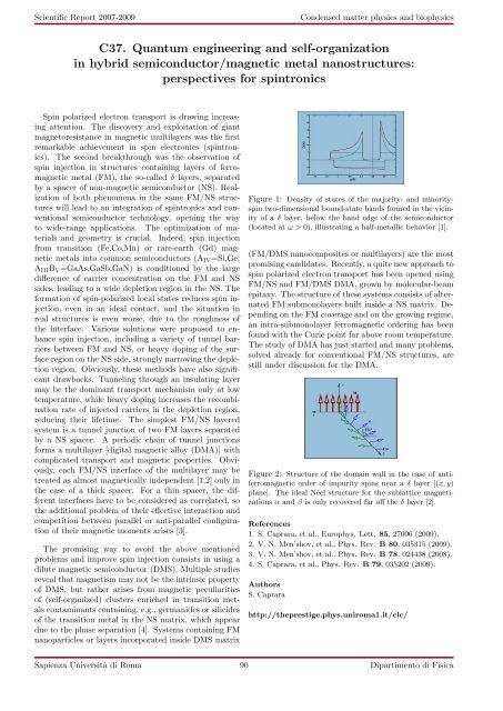
Figure 1: Density of states of the majority- and minorityspin<br />
two-dimensional bound-state bands formed in the vicinity<br />
of a δ layer, below the band edge of the semiconductor<br />
(located at ω > 0), illustrating a half-metallic behavior [1].<br />
(FM/DMS nanocomposites or multilayers) are the most<br />
promising candidates. Recently, a quite new approach to<br />
spin polarized electron transport has been opened using<br />
FM/NS and FM/DMS DMA, grown by molecular-beam<br />
epitaxy. The structure of these systems consists of alternated<br />
FM submonolayers built inside a NS matrix. Depending<br />
on the FM coverage and on the growing regime,<br />
an intra-submonolayer ferromagnetic ordering has been<br />
found with the Curie point far above room temperature.<br />
The study of DMA has just started and many problems,<br />
solved already for conventional FM/NS structures, are<br />
still under discussion for the DMA.<br />
Figure 2: Structure of the domain wall in the case of antiferromagnetic<br />
order of impurity spins near a δ layer [(x, y)<br />
plane]. The ideal Néel structure for the sublattice magnetizations<br />
α and β is only recovered far off the δ layer [2].<br />
References<br />
1. S. Caprara, et al., Europhys. Lett. 85, 27006 (2009).<br />
2. V. N. Men’shov, et al., Phys. Rev. B 80, 035315 (2009).<br />
3. V. N. Men’shov, et al., Phys. Rev. B 78, 024438 (2008).<br />
4. S. Caprara, et al., Phys. Rev. B 79, 035202 (2009).<br />
Authors<br />
S. Caprara<br />
http://theprestige.phys.uniroma1.it/clc/<br />
<strong>Sapienza</strong> Università di Roma 90 Dipartimento di Fisica